ICGOO在线商城 > 集成电路(IC) > 数据采集 - 数模转换器 > AD5744RCSUZ
 Datasheet下载
- 型号: AD5744RCSUZ
- 制造商: Analog
- 库位|库存: xxxx|xxxx
- 要求:
| 数量阶梯 | 香港交货 | 国内含税 |
| +xxxx | $xxxx | ¥xxxx |
查看当月历史价格
查看今年历史价格
AD5744RCSUZ产品简介:
ICGOO电子元器件商城为您提供AD5744RCSUZ由Analog设计生产,在icgoo商城现货销售,并且可以通过原厂、代理商等渠道进行代购。 AD5744RCSUZ价格参考¥275.14-¥275.14。AnalogAD5744RCSUZ封装/规格:数据采集 - 数模转换器, 14 位 数模转换器 4 32-TQFP(7x7)。您可以下载AD5744RCSUZ参考资料、Datasheet数据手册功能说明书,资料中有AD5744RCSUZ 详细功能的应用电路图电压和使用方法及教程。
AD5744RCSUZ 是由 Analog Devices Inc.(现为 Analog Devices, Inc., ADI)生产的一款高精度、低功耗的16位数模转换器(DAC),属于数据采集系统中的关键组件。该器件具有多种应用场景,特别是在需要高精度控制和信号处理的领域。

 1. 工业自动化与过程控制
在工业自动化和过程控制系统中,AD5744RCSUZ 可用于精确控制电机、阀门和其他执行机构。它能够将数字信号转换为模拟电压或电流输出,从而实现对设备的精确控制。例如,在温度、压力、流量等参数的闭环控制系统中,AD5744RCSUZ 可以确保传感器反馈的信号与设定值之间的误差最小化,提高系统的稳定性和响应速度。

 2. 测试与测量设备
AD5744RCSUZ 在测试与测量设备中也有广泛应用。它可以用于生成高精度的测试信号,帮助工程师校准仪器或验证电路性能。例如,在示波器、信号发生器等设备中,AD5744RCSUZ 可以为用户提供稳定的参考电压或电流,确保测试结果的准确性。

 3. 医疗设备
在医疗设备领域,AD5744RCSUZ 的高精度特性使其成为理想的选择。例如,在心电图机、超声设备、CT扫描仪等医疗器械中,它可用于精确控制信号的输出,确保诊断结果的可靠性。此外,AD5744RCSUZ 的低功耗特性也使得它适合应用于便携式医疗设备,延长电池寿命。

 4. 通信系统
在通信系统中,AD5744RCSUZ 可用于调制解调器、收发器等设备中,提供高精度的信号调理功能。它可以帮助实现更稳定的通信链路,减少信号失真和噪声干扰,尤其适用于对信号质量要求较高的无线通信系统。

 5. 汽车电子
在汽车电子领域,AD5744RCSUZ 可用于车载传感器、控制器等设备中,实现对车辆状态的实时监测和控制。例如,在自动驾驶系统中,它可以帮助精确调整传感器的输出信号,确保车辆的安全性和稳定性。

总之,AD5744RCSUZ 凭借其高精度、低功耗和广泛的适用性,成为了多个行业中的重要元件,尤其适合那些对信号精度和稳定性有严格要求的应用场景。
| 参数 | 数值 |
| 产品目录 | 集成电路 (IC)半导体 |
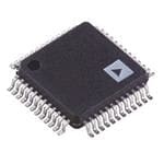
| 描述 | IC DAC 4CH 14BIT SER 1LSB 32TQFP数模转换器- DAC IC QUAD 14B SERIAL INPT +/-15V |
| 产品分类 | |
| 品牌 | Analog Devices Inc |
| 产品手册 | |
| 产品图片 |
|
| rohs | 符合RoHS无铅 / 符合限制有害物质指令(RoHS)规范要求 |
| 产品系列 | 数据转换器IC,数模转换器- DAC,Analog Devices AD5744RCSUZ- |
| 数据手册 | |
| 产品型号 | AD5744RCSUZ |
| PCN设计/规格 | |
| 产品培训模块 | http://www.digikey.cn/PTM/IndividualPTM.page?site=cn&lang=zhs&ptm=19145http://www.digikey.cn/PTM/IndividualPTM.page?site=cn&lang=zhs&ptm=18614http://www.digikey.cn/PTM/IndividualPTM.page?site=cn&lang=zhs&ptm=26125http://www.digikey.cn/PTM/IndividualPTM.page?site=cn&lang=zhs&ptm=26140http://www.digikey.cn/PTM/IndividualPTM.page?site=cn&lang=zhs&ptm=26150http://www.digikey.cn/PTM/IndividualPTM.page?site=cn&lang=zhs&ptm=26147 |
| 产品目录页面 | |
| 产品种类 | 数模转换器- DAC |
| 位数 | 14 |
| 供应商器件封装 | 32-TQFP(7x7) |
| 分辨率 | 14 bit |
| 包装 | 托盘 |
| 商标 | Analog Devices |
| 安装类型 | 表面贴装 |
| 安装风格 | SMD/SMT |
| 封装 | Tray |
| 封装/外壳 | 32-TQFP |
| 封装/箱体 | TQFP-48 |
| 工作温度 | -40°C ~ 85°C |
| 工厂包装数量 | 250 |
| 建立时间 | 10µs |
| 接口类型 | SPI |
| 数据接口 | 串行 |
| 最大功率耗散 | 387 mW |
| 最大工作温度 | + 85 C |
| 最小工作温度 | - 40 C |
| 标准包装 | 1 |
| 电压参考 | Internal, External |
| 电压源 | 模拟和数字,双 ± |
| 电源电压-最大 | 5.5 V |
| 电源电压-最小 | 2.7 V |
| 积分非线性 | +/- 1 LSB |
| 稳定时间 | 8 us |
| 系列 | AD5744R |
| 结构 | R-2R |
| 转换器数 | 4 |
| 转换器数量 | 4 |
| 输出数和类型 | 4 电压 |
| 输出类型 | Voltage |
| 采样比 | 1 MSPs |
| 采样率(每秒) | - |


- 商务部:美国ITC正式对集成电路等产品启动337调查
- 曝三星4nm工艺存在良率问题 高通将骁龙8 Gen1或转产台积电
- 太阳诱电将投资9.5亿元在常州建新厂生产MLCC 预计2023年完工
- 英特尔发布欧洲新工厂建设计划 深化IDM 2.0 战略
- 台积电先进制程称霸业界 有大客户加持明年业绩稳了
- 达到5530亿美元!SIA预计今年全球半导体销售额将创下新高
- 英特尔拟将自动驾驶子公司Mobileye上市 估值或超500亿美元
- 三星加码芯片和SET,合并消费电子和移动部门,撤换高东真等 CEO
- 三星电子宣布重大人事变动 还合并消费电子和移动部门
- 海关总署:前11个月进口集成电路产品价值2.52万亿元 增长14.8%


PDF Datasheet 数据手册内容提取
Complete Quad, 14-Bit, High Accuracy, Serial Input, Bipolar Voltage Output DAC Data Sheet AD5744R FEATURES GENERAL DESCRIPTION Complete quad, 14-bit digital-to-analog converter (DAC) The AD5744R is a quad, 14-bit, serial input, bipolar voltage output Programmable output range: ±10 V, ±10.2564 V, or DAC that operates from supply voltages of ±11.4 V to ±16.5 V. ±10.5263 V Nominal full-scale output range is ±10 V. The AD5744R provides ±1 LSB maximum INL error, ±1 LSB maximum DNL error integrated output amplifiers, reference buffers, and proprietary Low noise: 60 nV/√Hz power-up/power-down control circuitry. The part also features Settling time: 10 μs maximum a digital I/O port, programmed via the serial interface, and an Integrated reference buffers analog temperature sensor. The part incorporates digital offset Internal reference: 10 ppm/°C maximum and gain adjust registers per channel. On-chip die temperature sensor The AD5744R is a high performance converter that provides Output control during power-up/brownout guaranteed monotonicity, integral nonlinearity (INL) of ±1 LSB, Programmable short-circuit protection low noise, and 10 μs settling time. The AD5744R includes an on- Simultaneous updating via LDAC chip 5 V reference with a reference temperature coefficient of Asynchronous CLR to zero code 10 ppm/°C maximum. During power-up when the supply voltages Digital offset and gain adjust are changing, VOUTx is clamped to 0 V via a low impedance path. Logic output control pins DSP-/microcontroller-compatible serial interface The AD5744R is based on the iCMOS® technology platform, which Temperature range: −40°C to +85°C is designed for analog systems designers within industrial/instru- iCMOS process technology mentation equipment OEMs who need high performance ICs at higher voltage levels. iCMOS enables the development of analog APPLICATIONS ICs capable of 30 V and operation at ±15 V supplies, while allowing Industrial automation reductions in power consumption and package size, coupled with Open-loop/closed-loop servo control increased ac and dc performance. Process control The AD5744R uses a serial interface that operates at clock rates Data acquisition systems of up to 30 MHz and is compatible with DSP and microcontroller Automatic test equipment interface standards. Double buffering allows the simultaneous Automotive test and measurement updating of all DACs. The input coding is programmable to either High accuracy instrumentation twos complement or offset binary formats. The asynchronous clear function clears all DATA registers to either bipolar zero or zero scale, depending on the coding used. The AD5744R is ideal for both closed-loop servo control and open-loop control applications. The AD5744R is available in a 32-lead TQFP and offers guaranteed specifications over the −40°C to +85°C industrial temperature range (see Figure 1 for the functional block diagram). Rev. E Information furnished by Analog Devices is believed to be accurate and reliable. However, no responsibility is assumed by Analog Devices for its use, nor for any infringements of patents or other One Technology Way, P.O. Box 9106, Norwood, MA 02062-9106, U.S.A. rights of third parties that may result from its use. Specifications subject to change without notice. No license is granted by implication or otherwise under any patent or patent rights of Analog Devices. Tel: 781.329.4700 www.analog.com Trademarks and registered trademarks are the property of their respective owners. Fax: 781.461.3113 ©2008–2011 Analog Devices, Inc. All rights reserved.
AD5744R Data Sheet TABLE OF CONTENTS Features..............................................................................................1 Registers...........................................................................................24 Applications.......................................................................................1 Function Register.......................................................................24 General Description.........................................................................1 Data Register...............................................................................25 Revision History...............................................................................2 Coarse Gain Register.................................................................25 Functional Block Diagram..............................................................3 Fine Gain Register......................................................................25 Specifications.....................................................................................4 Design Features...............................................................................26 AC Performance Characteristics................................................6 Analog Output Control.............................................................26 Timing Characteristics................................................................7 Programmable Short-Circuit Protection................................26 Absolute Maximum Ratings..........................................................10 Digital I/O Port...........................................................................26 Thermal Resistance....................................................................10 Die Temperature Sensor............................................................26 ESD Caution................................................................................10 Local Ground Offset Adjust......................................................26 Pin Configuration and Function Descriptions...........................11 Applications Information..............................................................27 Typical Performance Characteristics...........................................13 Typical Operating Circuit.........................................................27 Terminology....................................................................................19 Layout Guidelines...........................................................................29 Theory of Operation......................................................................21 Galvanically Isolated Interface.................................................29 DAC Architecture.......................................................................21 Microprocessor Interfacing.......................................................29 Reference Buffers........................................................................21 Outline Dimensions.......................................................................30 Serial Interface............................................................................21 Ordering Guide..........................................................................30 Simultaneous Updating via LDAC...........................................23 Transfer Function.......................................................................23 Asynchronous Clear (CLR).......................................................23 REVISION HISTORY 9/11—Rev. D to Rev. E 2/09—Rev. A to Rev. B Changed 50 MHz to 30 MHz Throughout....................................1 Changes to Figure 1...........................................................................3 Changes to t, t, and t Parameters, Table 3..................................7 Changes to Table 1 Conditions and Added Endnote 1 2 3 to Table 1.............................................................................................4 7/11—Rev. C to Rev. D Added Endnote to Table 2................................................................6 Changed 30 MHz to 50 MHz Throughout....................................1 Added Endnote to Table 3................................................................7 Changes to t, t, and t Parameters, Table 3..................................7 Changes to Table 5..........................................................................10 1 2 3 8/09—Rev. B to Rev. C 1/09—Rev. 0 to Rev. A Deleted Endnote 1 in Table 1..........................................................4 Changes to Figure 1...........................................................................3 Deleted Endnote 1 in Table 2..........................................................6 Deleted Endnote 1 and Changes to t Parameter in Table 3 ......7 6 10/08—Revision 0: Initial Version Rev. E | Page 2 of 32
Data Sheet AD5744R FUNCTIONAL BLOCK DIAGRAM PGND AVDD AVSS AVDD AVSS REFOUT REFGND REFAB RSTOUT RSTIN VOLTAGE DVCC MONITOR AD5744R 5V REFERENCE AND DGND REFERENCE BUFFERS CONTROL ISCC 14 INPUT DATA 14 G1 SDIN INPUT REG A REG A DAC A VOUTA SHIFT G2 SCLK REGISTER SYNC COANNTDROL GAIN REG A AGNDA LOGIC SDO 14 G1 INPUT DATA REG B REG B DAC B VOUTB G2 GAIN REG B AGNDB D0 14 G1 INPUT DATA D1 REG C REG C DAC C VOUTC G2 GAIN REG C AGNDC BIN/2sCOMP 14 G1 INPUT DATA REG D REG D DAC D VOUTD G2 CLR GAIN REG D AGNDD REFERENCE TEMP BUFFERS SENSOR LDAC REFCD TEMP 06065-001 Figure 1. Rev. E | Page 3 of 32
AD5744R Data Sheet SPECIFICATIONS AV = 11.4 V to 16.5 V, AV = −11.4 V to −16.5 V, AGND = DGND = REFGND = PGND = 0 V; REFAB = REFCD = 5 V external; DD SS DV = 2.7 V to 5.25 V, R = 10 kΩ, C = 200 pF. All specifications T to T , unless otherwise noted. CC LOAD L MIN MAX Table 1. Parameter Min Typ Max Unit Test Conditions/Comments1 ACCURACY Outputs unloaded Resolution 14 Bits Relative Accuracy (INL) −1 +1 LSB Differential Nonlinearity (DNL) −1 +1 LSB Guaranteed monotonic Bipolar Zero Error −2 +2 mV 25°C; error at other temperatures obtained using bipolar zero tempco −3 +3 mV Bipolar Zero Tempco2 −2 +2 ppm FSR/°C Zero-Scale Error −2 +2 mV 25°C; error at other temperatures obtained using zero-scale tempco −2.5 +2.5 mV Zero-Scale Tempco2 −2 +2 ppm FSR/°C Gain Error −0.02 +0.02 % FSR Gain Tempco2 −2 +2 ppm FSR/°C DC Crosstalk2 0.125 LSB REFERENCE INPUT/OUTPUT Reference Input2 Reference Input Voltage 5 V ±1% for specified performance DC Input Impedance 1 MΩ Typically 100 MΩ Input Current −10 +10 μA Typically ±30 nA Reference Range 1 7 V Reference Output Output Voltage 4.995 5 5.005 V 25°C, AV /AV = ±13.5 V DD SS Reference Tempco2 −10 ±1.7 +10 ppm/°C R 2 1 MΩ LOAD Power Supply Sensitivity1 300 μV/V Output Noise2 18 μV p-p 0.1 Hz to 10 Hz Noise Spectral Density2 75 nV/√Hz 10 kHz Output Voltage Drift vs. Time2 ±40 ppm/500 hr ±50 ppm/1000 hr Thermal Hysteresis1 70 ppm First temperature cycle 30 ppm Subsequent temperature cycles OUTPUT CHARACTERISTICS2 Output Voltage Range3 −10.5263 +10.5263 V AV /AV = ±11.4 V, V = 5 V DD SS REFIN −14.7368 +14.7368 V AV /AV = ±16.5 V, V = 7 V DD SS REFIN Output Voltage Drift vs. Time ±13 ppm FSR/500 hr ±15 ppm FSR/1000 hr Short-Circuit Current 10 mA R = 6 kΩ, see Figure 31 ISCC Load Current −1 +1 mA For specified performance Capacitive Load Stability R = ∞ 200 pF LOAD R = 10 kΩ 1000 pF LOAD DC Output Impedance 0.3 Ω Rev. E | Page 4 of 32
Data Sheet AD5744R Parameter Min Typ Max Unit Test Conditions/Comments1 DIGITAL INPUTS2 DV = 2.7 V to 5.25 V CC Input High Voltage, V 2.4 V IH Input Low Voltage, V 0.8 V IL Input Current −1.2 +1.2 μA Per pin Pin Capacitance 10 pF Per pin DIGITAL OUTPUTS (D0, D1, SDO)2 Output Low Voltage 0.4 V DV = 5 V ± 5%, sinking 200 μA CC Output High Voltage DV − 1 V DV = 5 V ± 5%, sourcing 200 μA CC CC Output Low Voltage 0.4 V DV = 2.7 V to 3.6 V, sinking 200 μA CC Output High Voltage DV − 0.5 V DV = 2.7 V to 3.6 V, sourcing 200 μA CC CC High Impedance Leakage −1 +1 μA SDO only Current High Impedance Output 5 pF SDO only Capacitance DIE TEMPERATURE SENSOR2 Output Voltage at 25°C 1.47 V Die temperature Output Voltage Scale Factor 5 mV/°C Output Voltage Range 1.175 1.9 V −40°C to +105°C Output Load Current 200 μA Current source only Power-On Time 80 ms POWER REQUIREMENTS AV +11.4 +16.5 V DD AV −11.4 −16.5 V SS DV 2.7 5.25 V CC Power Supply Sensitivity2 ∆V /∆ΑV −85 dB OUT DD AI 3.55 mA/channel Outputs unloaded DD AI 2.8 mA/channel Outputs unloaded SS DI 1.2 mA V = DV , V = DGND, 750 μA typ CC IH CC IL Power Dissipation 275 mW ±12 V operation output unloaded 1 Temperature range: −40°C to +85°C; typical at +25°C. Device functionality is guaranteed to 105°C with degraded performance. 2 Guaranteed by design and characterization; not production tested. 3 Output amplifier headroom requirement is 1.4 V minimum. Rev. E | Page 5 of 32
AD5744R Data Sheet AC PERFORMANCE CHARACTERISTICS AV = 11.4 V to 16.5 V, AV = −11.4 V to −16.5 V, AGND = DGND = REFGND = PGND = 0 V; REFAB = REFCD = 5 V external; DD SS DV = 2.7 V to 5.25 V, R = 10 kΩ, C = 200 pF. All specifications T to T , unless otherwise noted. CC LOAD L MIN MAX Table 2. Parameter Min Typ Max Unit Test Conditions/Comments DYNAMIC PERFORMANCE1 Output Voltage Settling Time 8 μs Full-scale step to ±1 LSB 10 μs 2 μs 512 LSB step settling Slew Rate 5 V/μs Digital-to-Analog Glitch Energy 8 nV-sec Glitch Impulse Peak Amplitude 25 mV Channel-to-Channel Isolation 80 dB DAC-to-DAC Crosstalk 8 nV-sec Digital Crosstalk 2 nV-sec Digital Feedthrough 2 nV-sec Effect of input bus activity on DAC outputs Output Noise (0.1 Hz to 10 Hz) 0.025 LSB p-p Output Noise (0.1 Hz to 100 kHz) 45 μV rms 1/f Corner Frequency 1 kHz Output Noise Spectral Density 60 nV/√Hz Measured at 10 kHz Complete System Output Noise 80 nV/√Hz Measured at 10 kHz Spectral Density2 1 Guaranteed by design and characterization; not production tested. 2 Includes noise contributions from integrated reference buffers, 14-bit DAC, and output amplifier. Rev. E | Page 6 of 32
Data Sheet AD5744R TIMING CHARACTERISTICS AV = 11.4 V to 16.5 V, AV = −11.4 V to −16.5 V, AGND = DGND = REFGND = PGND = 0 V; REFAB = REFCD = 5 V external; DD SS DV = 2.7 V to 5.25 V, R = 10 kΩ, C = 200 pF. All specifications T to T , unless otherwise noted. CC LOAD L MIN MAX Table 3. Parameter1, 2, 3 Limit at T , T Unit Description MIN MAX t 33 ns min SCLK cycle time 1 t 13 ns min SCLK high time 2 t 13 ns min SCLK low time 3 t 13 ns min SYNC falling edge to SCLK falling edge setup time 4 t 4 13 ns min 24th SCLK falling edge to SYNC rising edge 5 t 90 ns min Minimum SYNC high time 6 t 2 ns min Data setup time 7 t 5 ns min Data hold time 8 t 1.7 μs min SYNC rising edge to LDAC falling edge (all DACs updated) 9 480 ns min SYNC rising edge to LDAC falling edge (single DAC updated) t 10 ns min LDAC pulse width low 10 t 500 ns max LDAC falling edge to DAC output response time 11 t 10 μs max DAC output settling time 12 t 10 ns min CLR pulse width low 13 t 2 μs max CLR pulse activation time 14 t 5, 6 25 ns max SCLK rising edge to SDO valid 15 t 13 ns min SYNC rising edge to SCLK falling edge 16 t 2 μs max SYNC rising edge to DAC output response time (LDAC = 0) 17 t 170 ns min LDAC falling edge to SYNC rising edge 18 1 Guaranteed by design and characterization; not production tested. 2 All input signals are specified with tR = tF = 5 ns (10% to 90% of DVCC) and timed from a voltage level of 1.2 V. 3 See Figure 2, Figure 3, and Figure 4. 4 Standalone mode only. 5 Measured with the load circuit of Figure 5. 6 Daisy-chain mode only. Rev. E | Page 7 of 32
AD5744R Data Sheet Timing Diagrams t 1 SCLK 1 2 24 t6 t3 t2 t4 t5 SYNC t 8 t 7 SDIN DB23 DB0 t10 t t10 9 LDAC t18 t12 t 11 VOUTx LDAC = 0 t 12 t 17 VOUTx t CLR 13 t 14 VOUTx 06065-002 Figure 2. Serial Interface Timing Diagram t 1 SCLK 24 48 t6 t3 t2 t5 t t 16 4 SYNC t 8 t 7 SDIN DB23 DB0 DB23 DB0 INPUT WORD FOR DAC N INPUT WORD FOR DAC N–1 t 15 SDO DB23 DB0 UNDEFINED INPUT WORD FOR DAC N t9 t 10 LDAC 06065-003 Figure 3. Daisy-Chain Timing Diagram Rev. E | Page 8 of 32
Data Sheet AD5744R SCLK 24 48 SYNC SDIN DB23 DB0 DB23 DB0 INPUT WORD SPECIFIES NOP CONDITION REGISTER TO BE READ SDO DB23 DB0 UNDEFINED SELECCTLEOD CRKEEGDIS OTUETR DATA 06065-004 Figure 4. Readback Timing Diagram 200µA IOL TO OUTPUT VOH (MIN) OR PIN CL VOL (MAX) 50pF 200µA IOH 06065-005 Figure 5. Load Circuit for SDO Timing Diagram Rev. E | Page 9 of 32
AD5744R Data Sheet ABSOLUTE MAXIMUM RATINGS T = 25°C, unless otherwise noted. Transient currents of up to Stresses above those listed under Absolute Maximum Ratings A 100 mA do not cause SCR latch-up. may cause permanent damage to the device. This is a stress rating only; functional operation of the device at these or any Table 4. other conditions above those indicated in the operational Parameter Rating section of this specification is not implied. Exposure to absolute AVDD to AGND, DGND −0.3 V to +17 V maximum rating conditions for extended periods may affect AVSS to AGND, DGND +0.3 V to −17 V device reliability. DV to DGND −0.3 V to +7 V CC Digital Inputs to DGND −0.3 V to (DV + 0.3 V) or +7 V, THERMAL RESISTANCE CC whichever is less θ is specified for the worst-case conditions, that is, a device JA Digital Outputs to DGND −0.3 V to DV + 0.3 V CC soldered in a circuit board for surface-mount packages. REFAB, REFCD to AGNDx, PGND −0.3 V to AV + 0.3 V DD REFOUT to AGNDx AVSS to AVDD Table 5. Thermal Resistance TEMP AVSS to AVDD Package Type θJA θ JC Unit VOUTx to AGNDx AVSS to AVDD 32-Lead TQFP 65 12 °C/W AGND to DGND −0.3 V to +0.3 V Operating Temperature Range ESD CAUTION Industrial −40°C to +85°C Storage Temperature Range −65°C to +150°C Junction Temperature (T max) 150°C J Lead Temperature (Soldering) JEDEC Industry Standard J-STD-020 Rev. E | Page 10 of 32
Data Sheet AD5744R PIN CONFIGURATION AND FUNCTION DESCRIPTIONS P M BIN/2sCO AVDDAVSS TEMP REFGND REFOUT REFCD REFAB 32 31 30 29 28 27 26 25 SYNC 1 24 AGNDA SCLK 2 PIN 1 23 VOUTA SDIN 3 AD5744R 22 VOUTB SDO 4 21 AGNDB TOP VIEW CLR 5 (Not to Scale) 20 AGNDC LDAC 6 19 VOUTC D0 7 18 VOUTD D1 8 17 AGNDD 9 10 11 12 13 14 15 16 T N D C D D S C RSTOU RSTI DGN DVCAVD PGN AVS ISC 06065-006 Figure 6. Pin Configuration Table 6. Pin Function Descriptions Pin No. Mnemonic Description 1 SYNC Active Low Input. This is the frame synchronization signal for the serial interface. While SYNC is low, data is transferred in on the falling edge of SCLK. 2 SCLK Serial Clock Input. Data is clocked into the shift register on the falling edge of SCLK. This operates at clock speeds of up to 30 MHz. 3 SDIN Serial Data Input. Data must be valid on the falling edge of SCLK. 4 SDO Serial Data Output. This pin is used to clock data from the serial register in daisy-chain or readback mode. 5 CLR Negative Edge Triggered Input.1 Asserting this pin sets the data register to 0x0000. 6 LDAC Load DAC. This logic input is used to update the data register and, consequently, the analog outputs. When tied permanently low, the addressed data register is updated on the rising edge of SYNC. If LDAC is held high during the write cycle, the DAC input register is updated, but the output update is held off until the falling edge of LDAC. In this mode, all analog outputs can be updated simultaneously on the falling edge of LDAC. The LDAC pin must not be left unconnected. 7, 8 D0, D1 Digital I/O Port. D0 and D1 form a digital I/O port. The user can set up these pins as inputs or outputs that are configurable and readable over the serial interface. When configured as inputs, these pins have weak internal pull-ups to DV . When programmed as outputs, D0 and D1 are referenced by DV and DGND. CC CC 9 RSTOUT Reset Logic Output. This is the output from the on-chip voltage monitor used in the reset circuit. If desired, it can be used to control other system components. 10 RSTIN Reset Logic Input. This input allows external access to the internal reset logic. Applying a Logic 0 to this input clamps the DAC outputs to 0 V. In normal operation, RSTIN should be tied to Logic 1. Register values remain unchanged. 11 DGND Digital Ground Pin. 12 DV Digital Supply Pin. Voltage ranges from 2.7 V to 5.25 V. CC 13, 31 AV Positive Analog Supply Pins. Voltage ranges from 11.4 V to 16.5 V. DD 14 PGND Ground Reference Point for Analog Circuitry. 15, 30 AV Negative Analog Supply Pins. Voltage ranges from –11.4 V to –16.5 V. SS 16 ISCC This pin is used in association with an optional external resistor to AGND to program the short-circuit current of the output amplifiers. Refer to the Design Features section for more information. 17 AGNDD Ground Reference Pin for DAC D Output Amplifier. 18 VOUTD Analog Output Voltage of DAC D. Buffered output with a nominal full-scale output range of ±10 V. The output amplifier is capable of directly driving a 10 kΩ, 200 pF load. 19 VOUTC Analog Output Voltage of DAC C. Buffered output with a nominal full-scale output range of ±10 V. The output amplifier is capable of directly driving a 10 kΩ, 200 pF load. 20 AGNDC Ground Reference Pin for DAC C Output Amplifier. 21 AGNDB Ground Reference Pin for DAC B Output Amplifier. 22 VOUTB Analog Output Voltage of DAC B. Buffered output with a nominal full-scale output range of ±10 V. The output amplifier is capable of directly driving a 10 kΩ, 200 pF load. Rev. E | Page 11 of 32
AD5744R Data Sheet Pin No. Mnemonic Description 23 VOUTA Analog Output Voltage of DAC A. Buffered output with a nominal full-scale output range of ±10 V. The output amplifier is capable of directly driving a 10 kΩ, 200 pF load. 24 AGNDA Ground Reference Pin for DAC A Output Amplifier. 25 REFAB External Reference Voltage Input for Channel A and Channel B. The reference input range is 1 V to 7 V, and it programs the full-scale output voltage. V = 5 V for specified performance. REFIN 26 REFCD External Reference Voltage Input for Channel C and Channel D. The reference input range is 1 V to 7 V, and it programs the full-scale output voltage. V = 5 V for specified performance. REFIN 27 REFOUT Reference Output. This is the reference output from the internal voltage reference. The internal reference is 5 V ± 3 mV at 25°C, with a reference temperature coefficient of 10 ppm/°C. 28 REFGND Reference Ground Return for the Reference Generator and Buffers. 29 TEMP This pin provides an output voltage proportional to temperature. The output voltage is 1.47 V typical at 25°C die temperature; variation with temperature is 5 mV/°C. 32 BIN/2sCOMP This pin determines the DAC coding. This pin should be hardwired to either DV or DGND. When hardwired to CC DV , input coding is offset binary (see Table 7). When hardwired to DGND, input coding is twos complement CC (see Table 8). 1 Internal pull-up device on this logic input. Therefore, it can be left floating; and it defaults to a logic high condition. Rev. E | Page 12 of 32
Data Sheet AD5744R TYPICAL PERFORMANCE CHARACTERISTICS 0.25 0.25 0.20 TVVADR DE=F/ VI2NS5 S°=C =5 V±15V 0.20 TVVADR DE=F/ VI2NS5 S°=C =5 V±12V 0.15 0.15 0.10 0.10 B) B) R (LS 0.05 R (LS 0.05 O 0 O 0 R R R R NL E–0.05 NL E–0.05 I–0.10 D–0.10 –0.15 –0.15 –0.20 –0.20 –0.25 –0.25 0 2000 4000 6000DA8C0 0C0OD1E0,000 12,000 14,000 16,000 06065-009 0 2000 4000 6000DA8C0 0C0OD1E0,000 12,000 14,000 16,000 06065-014 Figure 7. Integral Nonlinearity Error vs. DAC Code, Figure 10. Differential Nonlinearity Error vs. DAC Code, VDD/VSS = ±15 V VDD/VSS = ±12 V 0.25 0.12 TA = 25°C 0.20 VVDRDEF/VINS S= =5 V±12V 0.10 0.15 0.08 0.10 R (LSB) 0.05 R (LSB) 0.06 O 0 O 0.04 R R R R NL E–0.05 NL E 0.02 I–0.10 I 0 –0.15 –0.02 –0.20 VDD/VSS = ±15V REFIN = 5V –0.250 2000 4000 6000DA8C0 0C0OD1E0,000 12,000 14,000 16,000 06065-010 –0.04–40 –20 0 TEM2P0ERATU4R0E (°C)60 80 100 06065-015 Figure 8. Integral Nonlinearity Error vs. DAC Code, Figure 11. Integral Nonlinearity Error vs. Temperature, VDD/VSS = ±12 V VDD/VSS = ±15 V 0.25 0.12 TA = 25°C 0.20 VVDRDEF/VINS S= =5 V±15V 0.10 0.15 0.08 0.10 R (LSB) 0.05 R (LSB) 0.06 O 0 O 0.04 R R R R NL E–0.05 NL E 0.02 D–0.10 I 0 –0.15 –0.02 –0.20 VDD/VSS = ±12V REFIN = 5V –0.25 –0.04 0 2000 4000 6000DA8C0 0C0OD1E0,000 12,000 14,000 16,000 06065-013 –40 –20 0 TEM2P0ERATU4R0E (°C)60 80 100 06065-016 Figure 9. Differential Nonlinearity Error vs. DAC Code, Figure 12. Integral Nonlinearity Error vs. Temperature, VDD/VSS = ±15 V VDD/VSS = ±12 V Rev. E | Page 13 of 32
AD5744R Data Sheet 0.04 0.15 0.03 VVDRDEF/VINS S= =5 V±15V 0.10 TVAR E=F I2N5 °=C 5V 0.02 0.05 0.01 B) B) LS 0 LS 0 R ( R ( O–0.01 O–0.05 R R R R L E–0.02 L E–0.10 N N D D –0.03 –0.15 –0.04 –0.20 –0.05 –0.06 –0.25 –40 –20 0 TEM2P0ERATU4R0E (°C)60 80 100 06065-019 11.4 12.4 SU1P3P.4LY VOLTA14G.4E (V) 15.4 16.4 06065-025 Figure 13. Differential Nonlinearity Error vs. Temperature, Figure 16. Differential Nonlinearity Error vs. Supply Voltage VDD/VSS = ±15 V 0.04 0.20 VDD/VSS = ±12V 0.03 VREFIN = 5V 0.15 0.02 0.10 0.01 B) B) 0.05 R (LS 0 R (LS 0 O–0.01 O R R R R–0.05 DNL E––00..0032 INL E–0.10 –0.15 –0.04 –0.05 –0.20 TA = 25°C VDD/VSS = ±15V –0.06 –0.25 –40 –20 0 TEM2P0ERATU4R0E (°C)60 80 100 06065-020 1 2 RE3FERENCE 4VOLTAGE5 (V) 6 7 06065-027 Figure 14. Differential Nonlinearity Error vs. Temperature, Figure 17. Integral Nonlinearity Error vs. Reference Voltage VDD/VSS = ±12 V VDD/VSS = ±15 V 0.12 0.10 TA = 25°C –0.10 VREFIN = 5V 0.08 0.06 –0.08 0.04 R (LSB)–0.06 R (LSB) 0.02 O–0.04 O 0 R R R R NL E–0.02 NL E–0.02 I D–0.04 0 –0.06 –0.02 –0.08 TA = 25°C –0.04 –0.10 VDD/VSS = ±16.5V 11.4 12.4 SU1P3P.4LY VOLTA14G.4E (V) 15.4 16.4 06065-023 1 2 RE3FERENCE 4VOLTAGE5 (V) 6 7 06065-031 Figure 15. Integral Nonlinearity Error vs. Supply Voltage Figure 18. Differential Nonlinearity Error vs. Reference Voltage VDD/VSS = ±16.5 V Rev. E | Page 14 of 32
Data Sheet AD5744R 0.6 0.8 TA = 25°C VREFIN = 5V 0.4 VDD/VSS = ±15V 0.2 0.6 V) 0 m R ( 0.4 –0.2 RO VDD/VSS = ±12V UE (mV) ––00..64 ERO ER 0.2 T Z –0.8 LAR 0 –1.0 PO BI –1.2 –0.2 –1.4 –1.6 –0.4 1 2 RE3FERENCE 4VOLTAGE5 (V) 6 7 06065-035 –40 –20 0 TEM2P0ERATU4R0E (°C)60 80 100 06065-039 Figure 19. Total Unadjusted Error vs. Reference Voltage, Figure 22. Bipolar Zero Error vs. Temperature VDD/VSS = ±16.5 V 9.0 1.4 8.5 TVAR E=F I2N5 =°C 5V VREFIN = 5V 1.2 8.0 |IDD| 1.0 7.5 VDD/VSS = ±12V V) mA) 7.0 R (m 0.8 (S 6.5 RO 0.6 /IDDS 6.0 N ER I 5.5 |ISS| GAI 0.4 VDD/VSS = ±15V 0.2 5.0 4.5 0 4.011.4 12.4 13.4VDD/VSS (1V4).4 15.4 16.406065-037 –0.2–40 –20 0 TEM2P0ERATU4R0E (°C)60 80 100 06065-040 Figure 20. IDD/ISS vs. VDD/VSS Figure 23. Gain Error vs. Temperature 0.25 0.0014 VREFIN = 5V VDD/VSS = ±15V TA = 25°C 0.20 0.0013 0.15 5V mV) 0.10 VDD/VSS = ±12V 0.0012 OR ( 0.05 0.0011 E ERR 0 (mA)C0.0010 L C SCA–0.05 DI0.0009 O- R–0.10 ZE 0.0008 –0.15 3V 0.0007 –0.20 –0.25 0.0006 –40 –20 0 TEM2P0ERATU4R0E (°C)60 80 100 06065-038 0 0.5 1.0 1.5 2.0VLO2G.I5C (V)3.0 3.5 4.0 4.5 5.0 06065-041 Figure 21. Zero-Scale Error vs. Temperature Figure 24. DICC vs. Logic Input Voltage Rev. E | Page 15 of 32
AD5744R Data Sheet 7000 –4 TA = 25°C VREFIN = 5V –6 6000 VDD/VSS = ±15V –8 V) µ 5000 A ( VDD/VSS = ±12V –10 T EL 4000 –12 GE D mV) –14 LTA 3000 (OUT –16 O V T V 2000 –18 U P –20 UT 1000 VDD/VSS = ±12V, O –22 VREFIN = 5V, 0 TA = 25°C, –24 0x8000 TO 0x7FFF, 500ns/DIV –1000 –26 –10 –5SOURCE/SIN0K CURRENT (5mA) 10 06065-042 –2.0–1.5–1.0–0.5 0 0.51.01T.5IM2E.0 (µ2s.)53.03.54.04.55.05.56.0 06065-047 Figure 25. Source and Sink Capability of Output Amplifier with Positive Full Figure 28. Major Code Transition Glitch Energy, VDD/VSS = ±12 V Scale Loaded 10,000 TA = 25°C 9000 VREFIN = 5V VDD/VSS = ±15V MIDSCALE LOADED 8000 µV) VDD/VSS = ±15V VREFIN = 0V A ( 7000 T EL 6000 E D 5000 VDD/VSS = ±12V G A LT 4000 4 O T V 3000 U P 2000 T U O 1000 0 –1000–12 –7 SOURCE/–S2INK CURREN3T (mA) 8 06065-043 CH4 50.0µV M1.00s 50µVC/DHI4V 26µV 06065-048 Figure 26. Source and Sink Capability of Output Amplifier with Negative Full Figure 29. Peak-to-Peak Noise (100 kHz Bandwidth) Scale Loaded VDD/VSS = ±15V T TA = 25°C VREFIN = 5V VDD/VSS = ±12V, 1 VREFIN = 5V, TA = 25°C, 2 RAMP TIME = 100µs, LOAD = 200pF||10kΩ 3 1 1µs/DIV CH1 3.00V M1.00µs CH1 –120mV 06065-044 CCHH13 1100..00VmVBWBWCH2 10.0V MT 1 2090.µ6s0%A CH1 7.80mV 06065-055 Figure 27. Full-Scale Settling Time Figure 30. VOUTx vs. VDD/VSS on Power-Up Rev. E | Page 16 of 32
Data Sheet AD5744R 10 VDD/VSS = ±15V A) 98 TVAR E=F I2N5 °=C 5V VTAD D=/ V2S5S°C = ±12V m T ( 7 N E RR 6 U C T 5 UI RC 4 1 CI T- 3 R O H 2 S 1 0 5µV/DIV 0 20 40 RISC6C0 (kΩ) 80 100 120 06065-050 M1.00s A CH1 18mV 06065-053 Figure 31. Short-Circuit Current vs. RISCC Figure 34. REFOUT Output Noise 0.1 Hz to 10 Hz T VTAD D=/ V2S5S°C = ±12V 6 TVAD D=/ V2S5S°C = ±15V V) 5 E ( G A 1 LT 4 2 VO T U P 3 T U O E NC 2 E R E F 3 RE 1 CCHH13 150.0.00VVBBWW CH2 10.0V MT 4 2090.µ6s0%A CH1 7.80mV 06065-054 00 20 40 60LOA80D CU1R0R0EN1T2 (0µA)140 160 180 200 06065-032 Figure 32. REFOUT Turn-On Transient Figure 35. REFOUT Load Regulation 1.9 VT10ADµ D=F/ V 2CS5AS°C P=,A ±C1I2TVOR ON REFOUT V) 1.8 TVAD D=/ V2S5S°C = ±15V E ( G 1.7 A T L O 1.6 V T PU 1.5 1 T U O 1.4 E R TU 1.3 A R PE 1.2 M E T 1.1 50µV/DIV CH1 50.0µV M1.00s A CH1 15µV 06065-052 1.0–40 –20 0 TEM2P0ERATU4R0E (°C)60 80 100 06065-033 Figure 36. Temperature Output Voltage vs. Temperature Figure 33. REFOUT Output Noise 100 kHz Bandwidth Rev. E | Page 17 of 32
AD5744R Data Sheet 5.003 40 20 DEVICES SHOWN MAX: 10ppm/°C TYP: 1.7ppm/°C 35 V)5.002 GE ( 30 A OLT5.001 %) 25 PUT V5.000 TION ( 20 T A U L O U NCE 4.999 POP 15 E R 10 E F RE4.998 5 4.997–40 –20 0 TEM2P0ERATU4R0E(°C)60 80 100 06065-070 0 0.5 1.5 2.5TEM3P.5ERA4T.U5RE 5D.R5IFT6 (.p5pm/7°C.5) 8.5 9.5 06065-072 Figure 37. Reference Output Voltage vs. Temperature Figure 38. Reference Output Temperature Drift (−40°C to +85°C) Rev. E | Page 18 of 32
Data Sheet AD5744R TERMINOLOGY Total Unadjusted Error (TUE) Relative Accuracy or Integral Nonlinearity (INL) A measure of the output error, considering all the various For the DAC, a measure of the maximum deviation, in LSBs, errors. Figure 19 shows a plot of total unadjusted error vs. from a straight line passing through the endpoints of the DAC reference voltage. transfer function. Zero-Scale Error Temperature Coefficient Differential Nonlinearity (DNL) A measure of the change in zero-scale error with a change in The difference between the measured change and the ideal 1 LSB temperature. It is expressed as parts per million of full-scale change between any two adjacent codes. A specified differential range per degree Celsius (ppm FSR/°C). nonlinearity of ±1 LSB maximum ensures monotonicity. This DAC is guaranteed monotonic. Gain Error Temperature Coefficient A measure of the change in gain error with changes in tempera- Monotonicity ture. It is expressed as parts per million of full-scale range per A DAC is monotonic if the output either increases or remains degree Celsius (ppm FSR/°C). constant for increasing digital input code. The AD5744R is monotonic over its full operating temperature range. Digital-to-Analog Glitch Energy The impulse injected into the analog output when the input code Bipolar Zero Error in the data register changes state. It is normally specified as the The deviation of the analog output from the ideal half-scale area of the glitch in nanovolt-seconds (nV-sec) and is measured output of 0 V when the data register is loaded with 0x8000 when the digital input code is changed by 1 LSB at the major carry (offset binary coding) or 0x0000 (twos complement coding). transition (0x7FFF to 0x8000), as shown in Figure 28. Figure 22 shows a plot of bipolar zero error vs. temperature. Digital Feedthrough Bipolar Zero Temperature Coefficient A measure of the impulse injected into the analog output of the The measure of the change in the bipolar zero error with a DAC from the digital inputs of the DAC but is measured when change in temperature. It is expressed as parts per million of the DAC output is not updated. It is specified in nanovolt-seconds full-scale range per degree Celsius (ppm FSR/°C). (nV-sec) and measured with a full-scale code change on the Full-Scale Error data bus, that is, from all 0s to all 1s, and vice versa. The measure of the output error when full-scale code is loaded Power Supply Sensitivity to the data register. Ideally, the output voltage should be 2 × Indicates how the output of the DAC is affected by changes in V − 1 LSB. Full-scale error is expressed as a percentage of REFIN the power supply voltage. full-scale range (% FSR). DC Crosstalk Negative Full-Scale Error/Zero-Scale Error The dc change in the output level of one DAC in response to a The error in the DAC output voltage when 0x0000 (offset binary change in the output of another DAC. It is measured with a full- coding) or 0x8000 (twos complement coding) is loaded to the scale output change on one DAC while monitoring another data register. Ideally, the output voltage should be −2 × V . REFIN DAC, and is expressed in least significant bits (LSBs). Figure 21 shows a plot of zero-scale error vs. temperature. DAC-to-DAC Crosstalk Output Voltage Settling Time The glitch impulse transferred to the output of one DAC due The amount of time it takes for the output to settle to a specified to a digital code change and subsequent output change of level for a full-scale input change. another DAC. This includes both digital and analog crosstalk. Slew Rate It is measured by loading one of the DACs with a full-scale code A limitation in the rate of change of the output voltage. The output change (from all 0s to all 1s, and vice versa) with LDAC low and slewing speed of a voltage output DAC is usually limited by the monitoring the output of another DAC. The energy of the glitch slew rate of the amplifier used at its output. Slew rate is measured is expressed in nanovolt-seconds (nV-sec). from 10% to 90% of the output signal and is given in volts per Channel-to-Channel Isolation microsecond (V/μs). The ratio of the amplitude of the signal at the output of one DAC Gain Error to a sine wave on the reference input of another DAC. It is A measure of the span error of the DAC. It is the deviation in measured in decibels (dB). slope of the DAC transfer characteristic from the ideal, expressed Reference Temperature Coefficient as a percentage of the full-scale range (% FSR). Figure 23 shows a plot of gain error vs. temperature. A measure of the change in the reference output voltage with a change in temperature. It is expressed in parts per million per degree Celsius (ppm/°C). Rev. E | Page 19 of 32
AD5744R Data Sheet Digital Crosstalk Thermal Hysteresis A measure of the impulse injected into the analog output of one The change of reference output voltage after the device is cycled DAC from the digital inputs of another DAC but is measured through temperatures from −40°C to +85°C and back to −40°C. when the DAC output is not updated. It is specified in nanovolt- This is a typical value from a sample of parts put through such seconds (nV-sec) and measured with a full-scale code change a cycle. on the data bus; that is, from all 0s to all 1s, and vice versa. Rev. E | Page 20 of 32
Data Sheet AD5744R THEORY OF OPERATION The AD5744R is a quad, 14-bit, serial input, bipolar voltage output SERIAL INTERFACE DAC that operates from supply voltages of ±11.4 V to ±16.5 V and The AD5744R is controlled over a versatile 3-wire serial interface has a buffered output voltage of up to ±10.5263 V. Data is written to that operates at clock rates of up to 30 MHz and is compatible the AD5744R in a 24-bit word format via a 3-wire serial interface. with SPI, QSPI™, MICROWIRE™, and DSP standards. The AD5744R also offers an SDO pin that is available for daisy Input Shift Register chaining or readback. The input shift register is 24 bits wide. Data is loaded into the The AD5744R incorporates a power-on reset circuit that ensures device, MSB first, as a 24-bit word under the control of a serial that the data registers are loaded with 0x0000 at power-up. The clock input, SCLK. The input register consists of a read/write bit, AD5744R features a digital I/O port that can be programmed via a reserved bit that must be set to 0, three register select bits, three the serial interface, an analog die temperature sensor, on-chip DAC address bits, and 16 data bits, as shown in Table 9. The timing 10 ppm/°C voltage reference, on-chip reference buffers, and per diagram for this operation is shown in Figure 2. channel digital gain and offset registers. Upon power-up, the data registers are loaded with zero code DAC ARCHITECTURE (0x0000), and the outputs are clamped to 0 V via a low impedance The DAC architecture of the AD5744R consists of a 14-bit current path. The outputs can be updated with the zero code value by mode segmented R-2R DAC. The simplified circuit diagram for asserting either LDAC or CLR. The corresponding output voltage the DAC section is shown in Figure 39. depends on the state of the BIN/2sCOMP pin. If the BIN/2sCOMP VREF R R R pin is tied to DGND, the data coding is twos complement and the outputs update to 0 V. If the BIN/2sCOMP pin is tied to DV , CC 2R 2R 2R 2R 2R 2R 2R the data coding is offset binary and the outputs update to negative full scale. To have the outputs power-up with zero code loaded R/8 E15 E14 E1 S11 S10 S0 to the outputs, the CLR pin should be held low during power-up. IOUT Standalone Operation VOUTx The serial interface works with both a continuous and noncon- AGNDx 41 M5 SEBQsU DAELC SOEDGEMDE INNTTSO 12-BIT, R-2R LADDER 06065-060 tifi nSuYoNuCs s iesr hiaell dcl loocwk .f oAr cthoen tcionruroecuts nSuCmLbKe rs oouf rccloe ccka ncy bcele us.s Iend goantelyd Figure 39. DAC Ladder Structure clock mode, a burst clock containing the exact number of clock The four MSBs of the 14-bit data-word are decoded to drive cycles must be used, and SYNC must be taken high after the final 15 switches, E1 to E15. Each of these switches connects one of clock to latch the data. The first falling edge of SYNC starts the the 15 matched resistors to either AGNDx or I . The remaining OUT write cycle. Exactly 24 falling clock edges must be applied to SCLK 12 bits of the data-word drive Switch S0 to Switch S11 of the 12-bit before SYNC is brought high again. If SYNC is brought high before R-2R ladder network. the 24th falling SCLK edge, the data written is invalid. If more REFERENCE BUFFERS than 24 falling SCLK edges are applied before SYNC is brought The AD5744R can operate with either an external or an internal high, the input data is also invalid. The input register addressed is reference. The reference inputs (REFAB and REFCD) have an updated on the rising edge of SYNC. For another serial transfer to input range of up to 7 V. This input voltage is then used to provide take place, SYNC must be brought low again. After the end of a buffered positive and negative reference for the DAC cores. the serial data transfer, data is automatically transferred from the The positive reference is given by input shift register to the addressed register. +V = 2 × V When the data has been transferred into the chosen register of REF REFIN the addressed DAC, all data registers and outputs can be The negative reference to the DAC cores is given by updated by taking LDAC low. −V = −2 × V REF REFIN These positive and negative reference voltages (along with the gain register values) define the output ranges of the DACs. Rev. E | Page 21 of 32
AD5744R Data Sheet the system requires 24 clock pulses. Therefore, the total number 68HC11* AD5744R* of clock cycles must equal 24n, where n is the total number of MOSI SDIN AD5744R devices in the chain. When the serial transfer to all SCK SCLK devices is complete, SYNC is taken high. This latches the input PC7 SYNC data in each device in the daisy chain and prevents any further PC6 LDAC data from being clocked into the input shift register. The serial MISO SDO clock can be a continuous or a gated clock. A continuous SCLK source can be used only if SYNC is held SDIN low for the correct number of clock cycles. In gated clock mode, AD5744R* a burst clock containing the exact number of clock cycles must SCLK be used, and SYNC must be taken high after the final clock to SYNC latch the data. LDAC Readback Operation SDO Before a readback operation is initiated, the SDO pin must be enabled by writing to the function register and clearing the SDO SDIN disable bit; this bit is cleared by default. Readback mode is invoked AD5744R* by setting the R/W bit to 1 in the serial input register write. SCLK With R/W set to 1, Bit A2 to Bit A0, in association with Bit REG2, SYNC to Bit REG0, select the register to be read. The remaining data LDAC bits in the write sequence are don’t care. During the next SPI write, SDO the data appearing on the SDO output contain the data from the *ADDITIONAL PINS OMITTED FOR CLARITY. 06065-061 pNrOevPio cuosmlym adanddre csasend b ree guissetder i. nF oclro ac kreinagd oouf ta t shien dglaet ar efrgoismte trh, eth e Figure 40. Daisy-Chaining the AD5744R selected register on SDO. The readback diagram in Figure 4 shows the readback sequence. For example, to read back the fine gain Daisy-Chain Operation register of Channel A, implement the following sequence: For systems that contain several devices, the SDO pin can be 1. Write 0xA0XXXX to the input register. This write configures used to daisy-chain several devices together. This daisy-chain the AD5744R for read mode with the fine gain register of mode can be useful in system diagnostics and in reducing the Channel A selected. Note that all the data bits, DB15 to DB0, number of serial interface lines. The first falling edge of SYNC are don’t care. starts the write cycle. The SCLK is continuously applied to the input shift register when SYNC is low. If more than 24 clock 2. Follow with a second write: an NOP condition, 0x00XXXX. During this write, the data from the fine gain register is pulses are applied, the data ripples out of the shift register and clocked out on the SDO line; that is, data clocked out contains appears on the SDO line. This data is clocked out on the rising the data from the fine gain register in Bit DB5 to Bit DB0. edge of SCLK and is valid on the falling edge. By connecting the SDO of the first device to the SDIN input of the next device in the chain, a multidevice interface is constructed. Each device in Rev. E | Page 22 of 32
Data Sheet AD5744R SIMULTANEOUS UPDATING VIA LDAC TRANSFER FUNCTION Depending on the status of both SYNC and LDAC, and after Table 7 and Table 8 show the ideal input code to output voltage data has been transferred into the input register of the DACs, relationship for offset binary data coding and twos complement there are two ways to update the data registers and DAC outputs. data coding, respectively. Individual DAC Updating The output voltage expression for the AD5744R is given by In individual DAC updating mode, LDAC is held low while data ⎡ D ⎤ V = −2 × V + 4 × V OUT REFIN REFIN⎢ ⎥ is being clocked into the input shift register. The addressed ⎣16,384⎦ DAC output is updated on the rising edge of SYNC. where: Simultaneous Updating of All DACs D is the decimal equivalent of the code loaded to the DAC. V is the reference voltage applied at the REFAB and In simultaneous updating of all DACs mode, LDAC is held high REFIN REFCD pins. while data is being clocked into the input shift register. All DAC outputs are updated by taking LDAC low any time after SYNC ASYNCHRONOUS CLEAR (CLR) has been taken high. The update then occurs on the falling edge of LDAC. CLR is a negative edge triggered clear that allows the outputs to be cleared to either 0 V (twos complement coding) or negative full See Figure 41 for a simplified block diagram of the DAC load scale (offset binary coding). It is necessary to maintain CLR low circuitry. for a minimum amount of time for the operation to complete OUTPUT I/V AMPLIFIER (see Figure 2). When the CLR signal is returned high, the output REFAB, REFCD 14-BIT VOUTx remains at the cleared value until a new value is programmed. DAC If CLR is at 0 V at power-on, all DAC outputs are updated with the clear value. A clear can also be initiated through software by LDAC REDGAISTTAER writing the command of 0x04XXXX to the AD5744R. INPUT REGISTER SSSYCDNLICNK INTLEORGFIACCE SDO 06065-062 Figure 41. Simplified Serial Interface of Input Loading Circuitry for One DAC Channel Table 7. Ideal Output Voltage to Input Code Relationship—Offset Binary Data Coding Digital Input Analog Output MSB LSB V OUT 11 1111 1111 1111 +2 V × (8191/8192) REF 10 0000 0000 0001 +2 V × (1/8192) REF 10 0000 0000 0000 0 V 01 1111 1111 1111 −2 VREF × (1/8192) 00 0000 0000 0000 −2 VREF × (8191/8192) Table 8. Ideal Output Voltage to Input Code Relationship—Twos Complement Data Coding Digital Input Analog Output MSB LSB V OUT 01 1111 1111 1111 +2 V × (8191/8192) REF 00 0000 0000 0001 +2 V × (1/8192) REF 00 0000 0000 0000 0 V 11 1111 1111 1111 −2 VREF × (1/8192) 10 0000 0000 0000 −2 VREF × (8191/8192) Rev. E | Page 23 of 32
AD5744R Data Sheet REGISTERS Table 9. Input Shift Register Format MSB LSB DB23 DB22 DB21 DB20 DB19 DB18 DB17 DB16 DB15 to DB0 R/W 0 REG2 REG1 REG0 A2 A1 A0 Data Table 10. Input Shift Register Bit Function Descriptions Register Bit Description R/W Indicates a read from or a write to the addressed register REG2, REG1, REG0 Used in association with the address bits, determines if a read or write operation is to the data register, offset register, gain register, or function register. REG2 REG1 REG0 Function 0 0 0 Function register 0 1 0 Data register 0 1 1 Coarse gain register 1 0 0 Fine gain register A2, A1, A0 Decodes the DAC channels A2 A1 A0 Channel Address 0 0 0 DAC A 0 0 1 DAC B 0 1 0 DAC C 0 1 1 DAC D 1 0 0 All DACs Data Data bits FUNCTION REGISTER The function register is addressed by setting the three REG bits to 000. The values written to the address bits and the data bits determine the function addressed. The functions available via the function register are outlined in Table 11 and Table 12. Table 11. Function Register Options REG2 REG1 REG0 A2 A1 A0 DB15 to DB6 DB5 DB4 DB3 DB2 DB1 DB0 0 0 0 0 0 0 NOP, data = don’t care 0 0 0 0 0 1 Don’t care Local ground D1 D1 D0 D0 SDO offset adjust direction value direction value disable 0 0 0 1 0 0 Clear, data = don’t care 0 0 0 1 0 1 Load, data = don’t care Table 12. Explanation of Function Register Options Option Description NOP No operation instruction used in readback operations. Local Ground Set by the user to enable the local ground offset adjust function. Offset Adjust Cleared by the user to disable the local ground offset adjust function (default). See the Design Features section for more information. D0, D1 Direction Set by the user to enable the D0 and D1 pins as outputs. Cleared by the user to enable the D0 and D1 pins as inputs (default). See the Design Features section for more information. D0, D1 Value I/O port status bits. Logic values written to these locations determine the logic outputs on the D0 and D1 pins when configured as outputs. These bits indicate the status of the D0 and D1 pins when the I/O port is active as an input. When enabled as inputs, these bits are don’t cares during a write operation. SDO Disable Set by the user to disable the SDO output. Cleared by the user to enable the SDO output (default). Clear Addressing this function resets the DAC outputs to 0 V in twos complement mode and negative full scale in binary mode. Load Addressing this function updates the data registers and, consequently, the analog outputs. Rev. E | Page 24 of 32
Data Sheet AD5744R DATA REGISTER The data register is addressed by setting the three REG bits to 010. The DAC address bits select the DAC channel with which the data transfer takes place (see Table 10). The data bits are positioned in DB15 to DB2, as shown in Table 13. Table 13. Programming the Data Register REG2 REG1 REG0 A2 A1 A0 DB15 to DB2 DB1 DB0 0 1 0 DAC address 14-bit DAC data X X COARSE GAIN REGISTER The coarse gain register is addressed by setting the three REG bits to 011. The DAC address bits select the DAC channel with which the data transfer takes place (see Table 10). The coarse gain register is a 2-bit register that allows the user to select the output range of each DAC as shown in Table 15. Table 14. Programming the Coarse Gain Register REG2 REG1 REG0 A2 A1 A0 DB15 to DB2 DB1 DB0 0 1 1 DAC address Don’t care CG1 CG0 Table 15. Output Range Selection Output Range CG1 CG0 ±10 V (Default) 0 0 ±10.2564 V 0 1 ±10.5263 V 1 0 FINE GAIN REGISTER The fine gain register is addressed by setting the three REG bits to 100. The DAC address bits select the DAC channel with which the data transfer takes place (see Table 10). The AD5744R fine gain register is a 6-bit register that allows the user to adjust the gain of each DAC channel by −8 LSBs to +7.75 LSBs in 0.25 LSB steps, as shown in Table 16 and Table 17. The adjustment is made to both the positive full- scale points and the negative full-scale points simultaneously, with each point adjusted by one-half of one step. The fine gain register coding is twos complement. Table 16. Programming the Fine Gain Register REG2 REG1 REG0 A2 A1 A0 DB15 to DB6 DB5 DB4 DB3 DB2 DB1 DB0 1 0 0 DAC address Don’t care FG5 FG4 FG3 FG2 FG1 FG0 Table 17. Fine Gain Register Options Gain Adjustment FG5 FG4 FG3 FG2 FG1 FG0 +7.75 LSBs 0 1 1 1 1 1 +7.5 LSBs 0 1 1 1 1 0 No Adjustment (Default) 0 0 0 0 0 0 −7.75 LSBs 1 0 0 0 0 1 −8 LSBs 1 0 0 0 0 0 Rev. E | Page 25 of 32
AD5744R Data Sheet DESIGN FEATURES ANALOG OUTPUT CONTROL If the ISCC pin is left unconnected, the short-circuit current limit defaults to 5 mA. It should be noted that limiting the short- In many industrial process control applications, it is vital that circuit current to a small value can affect the slew rate of the the output voltage be controlled during power-up and during output when driving into a capacitive load. Therefore, the value brownout conditions. When the supply voltages are changing, of the short-circuit current that is programmed should take into the VOUTx pins are clamped to 0 V via a low impedance path. account the size of the capacitive load being driven. To prevent the output amp from being shorted to 0 V during this DIGITAL I/O PORT time, Transmission Gate G1 is also opened (see Figure 42). RSTOUT RSTIN The AD5744R contains a 2-bit digital I/O port (D1 and D0). These bits can be configured independently as inputs or outputs VOLTAGE and can be driven or have their values read back via the serial MONITOR AND interface. The I/O port signals are referenced to DVCC and DGND. CONTROL When configured as outputs, they can be used as control signals to multiplexers or can be used to control calibration circuitry G1 VOUTA elsewhere in the system. When configured as inputs, the logic G2 signals from limit switches, for example, can be applied to D0 AGNDA 06065-063 aDnIdE D T1E aMndP EcaRnA bTe UreRadE b SaEckN uSsOinRg t he digital interface. Figure 42. Analog Output Control Circuitry The on-chip die temperature sensor provides a voltage output that These conditions are maintained until the power supplies stabilize is linearly proportional to the Celsius temperature scale. Its nom- and a valid word is written to the data register. G2 then opens, and inal output voltage is 1.47 V at 25°C die temperature, varying at G1 closes. Both transmission gates are also externally controllable 5 mV/°C, giving a typical output range of 1.175 V to 1.9 V over the via the reset in (RSTIN) control input. For example, if RSTIN is full temperature range. Its low output impedance and linear output driven from a battery supervisor chip, the RSTIN input is driven simplify interfacing to temperature control circuitry and analog-to- low to open G1 and close G2 on power-off or during a brownout. digital converters (ADCs). The temperature sensor is provided Conversely, the on-chip voltage detector output (RSTOUT) is as more of a convenience than as a precise feature; it is intended also available to the user to control other parts of the system. for indicating a die temperature change for recalibration purposes. The basic transmission gate functionality is shown in Figure 42. LOCAL GROUND OFFSET ADJUST PROGRAMMABLE SHORT-CIRCUIT PROTECTION The AD5744R incorporates a local ground offset adjust feature The short-circuit current (I ) of the output amplifiers can be SC that, when enabled in the function register, adjusts the DAC programmed by inserting an external resistor between the ISCC outputs for voltage differences between the individual DAC ground pin and the PGND pin. The programmable range for the current is pins and the REFGND pin, ensuring that the DAC output voltages 500 μA to 10 mA, corresponding to a resistor range of 120 kΩ to are always referenced to the local DAC ground pin. For example, if 6 kΩ . The resistor value is calculated as follows: the AGNDA pin is at +5 mV with respect to the REFGND pin, and 60 VOUTA is measured with respect to AGNDA, a −5 mV error R ≈ I results, enabling the local ground offset adjust feature to adjust SC VOUTA by +5 mV, thereby eliminating the error. Rev. E | Page 26 of 32
Data Sheet AD5744R APPLICATIONS INFORMATION TYPICAL OPERATING CIRCUIT Initial accuracy error on the output voltage of an external refer- ence could lead to a full-scale error in the DAC. Therefore, to Figure 43 shows the typical operating circuit for the AD5744R. minimize these errors, a reference with low initial accuracy The only external components needed for this precision 14-bit error specification is preferred. Choosing a reference with an DAC are decoupling capacitors on the supply pins and reference output trim adjustment, such as the ADR425, allows a system inputs and an optional short-circuit current setting resistor. designer to trim system errors out by setting the reference Because the AD5744R incorporates a voltage reference and voltage to a voltage other than the nominal. The trim adjustment reference buffers, it eliminates the need for an external bipolar can also be used at temperature to trim out any error. reference and associated buffers, resulting in an overall savings in both cost and board space. Long term drift is a measure of how much the reference output voltage drifts over time. A reference with a tight long-term drift In Figure 43, AV is connected to +15 V, and AV is connected DD SS specification ensures that the overall solution remains relatively to −15 V; but AV and AV can operate with supplies from DD SS stable over its entire lifetime. ±11.4 V to ±16.5 V. In Figure 43, AGNDx is connected to REFGND. The temperature coefficient of a reference output voltage affects INL, DNL, and TUE. A reference with a tight temperature coef- Precision Voltage Reference Selection ficient specification should be chosen to reduce the dependence To achieve the optimum performance from the AD5744R over of the DAC output voltage on ambient conditions. its full operating temperature range, an external voltage reference In high accuracy applications, which have a relatively low noise must be used. Care must be taken in the selection of a precision budget, reference output voltage noise must be considered. It is voltage reference. The AD5744R has two reference inputs, REFAB important to choose a reference with as low an output noise and REFCD. The voltages applied to the reference inputs are used voltage as practical for the system resolution that is required. to provide a buffered positive and negative reference for the DAC Precision voltage references, such as the ADR435 (XFET® design), cores. Therefore, any error in the voltage reference is reflected produce low output noise in the 0.1 Hz to 10 Hz region. However, in the outputs of the device. as the circuit bandwidth increases, filtering the output of the There are four possible sources of error to consider when choosing reference may be required to minimize the output noise. a voltage reference for high accuracy applications: initial accuracy, temperature coefficient of the output voltage, long term drift, and output voltage noise. Table 18. Some Precision References Recommended for Use with the AD5744R Initial Accuracy Long-Term Drift Temperature Drift 0.1 Hz to 10 Hz Noise Part No. (mV Maximum) (ppm Typical) (ppm/°C Maximum) (μV p-p Typical) ADR435 ±6 30 3 3.5 ADR425 ±6 50 3 3.4 ADR02 ±5 50 3 10 ADR395 ±6 50 25 5 AD586 ±2.5 15 10 4 Rev. E | Page 27 of 32
AD5744R Data Sheet +15V –15V 10µF 10µF 100nF 100nF TEMP µF 0 1 BIN/2sCOMP 32 31 30 29 28 27 26 25 +5V P D S P D T D B SYNC 1 SYNC N/2sCOM AVDAVS TEM REFGN REFOU REFC REFAAGNDA 24 SCLK 2 SCLK BI VOUTA 23 VOUTA SDIN 3 SDIN VOUTB 22 VOUTB SDO 4 SDO AD5744R AGNDB 21 5 CLR AGNDC 20 LDAC 6 LDAC VOUTC 19 VOUTC D0 7 D0 VOUTD 18 VOUTD D1 8 D1 T AGNDD 17 RSTOU RSTIN DGND DVCCAVDDPGND AVSSISCC 9 10 11 12 13 14 15 16 RSTOUT nF nF 0 0 RSTIN 10µ10F 10 0µF 1 100nF 10µF +5V +15V –15V 06065-064 Figure 43. Typical Operating Circuit Rev. E | Page 28 of 32
Data Sheet AD5744R LAYOUT GUIDELINES In any circuit where accuracy is important, careful considera- through on the board. A microstrip technique is recommended tion of the power supply and ground return layout helps to ensure but not always possible with a double-sided board. In this the rated performance. Design the PCB on which the AD5744R technique, the component side of the board is dedicated to the is mounted such that the analog and digital sections are separated ground plane, and the signal traces are placed on the solder side. and confined to certain areas of the board. If the AD5744R is in GALVANICALLY ISOLATED INTERFACE a system where multiple devices require an AGNDx-to-DGND In many process control applications, it is necessary to provide connection, establish the connection at one point only. Establish an isolation barrier between the controller and the unit being the star ground point as close as possible to the device. The controlled to protect and isolate the controlling circuitry from AD5744R should have ample supply bypassing of 10 μF in parallel any hazardous common-mode voltages that may occur. Isocou- with 0.1 μF on each supply located as close to the package as plers provide voltage isolation in excess of 2.5 kV. The serial possible, ideally right up against the device. The 10 μF capaci- loading structure of the AD5744R makes it ideal for isolated tors are of the tantalum bead type. The 0.1 μF capacitor should interfaces because the number of interface lines is kept to a min- have low effective series resistance (ESR) and low effective series imum. Figure 44 shows a 4-channel isolated interface to the inductance (ESI), such as the common ceramic types that AD5744R using an ADuM1400 iCoupler® product. For more provide a low impedance path to ground at high frequencies to information on iCoupler products, refer to www.analog.com. handle transient currents due to internal logic switching. MICROPROCESSOR INTERFACING The power supply lines of the AD5744R should use as large a trace as possible to provide low impedance paths and reduce Microprocessor interfacing to the AD5744R is accomplished the effects of glitches on the power supply line. Shield fast- using a serial bus that uses standard protocol that is compatible switching signals, such as clocks with digital ground to avoid with microcontrollers and DSP processors. The communications radiating noise to other parts of the board; they should never be channel is a 3-wire (minimum) interface consisting of a clock run near the reference inputs. A ground line routed between signal, a data signal, and a synchronization signal. The AD5744R the SDIN and SCLK lines helps reduce cross-talk between them. requires a 24-bit data-word with data valid on the falling edge (A ground line is not required on a multi-layer board because of SCLK. it has a separate ground plane; however, it is helpful to separate For all the interfaces, a DAC output update can be performed the lines.) It is essential to minimize noise on the reference inputs automatically when all the data is clocked in, or it can be done because it couples through to the DAC output. Avoid crossover under the control of LDAC. The contents of the data register of digital and analog signals. Run traces on opposite sides of the can be read using the readback function. board at right angles to each other to reduce the effects of feed- MICROCONTROLLER ADuM1400* SERIAL CLOCK OUT VIA ENCODE DECODE VOA TO SCLK SERIAL DATA OUT VIB ENCODE DECODE VOB TO SDIN SYNC OUT VIC ENCODE DECODE VOC TO SYNC CONTROL OUT VID ENCODE DECODE VOD TO LDAC *ADDITIONAL PINS OMITTED FOR CLARITY. 06065-065 Figure 44. Isolated Interface Rev. E | Page 29 of 32
AD5744R Data Sheet OUTLINE DIMENSIONS 0.75 1.20 MAX 9.00 BSC SQ 0.60 0.45 32 25 1 24 PIN 1 7.00 TOP VIEW BSC SQ 1.05 0° MIN 0.20 (PINS DOWN) 1.00 0.09 0.95 7° 3.5° 8 17 0.15 SEATING 0° 9 16 0.05 PLANE 0C.O08P LMAANXARITY VIEW A 0.80 0.45 BSC VIEW A LEAD PITCH 0.37 0.30 ROTATED 90° CCW COMPLIANTTO JEDEC STANDARDS MS-026-ABA 020607-A Figure 45. 32-Lead Thin Plastic Quad Flat Package [TQFP] (SU-32-2) Dimensions shown in millimeters ORDERING GUIDE Internal Package Model1 Function INL Temperature Range Reference Package Description Option AD5744RCSUZ Quad 14-Bit DAC ±1 LSB Maximum −40°C to +85°C +5 V 32-Lead TQFP SU-32-2 AD5744RCSUZ-REEL7 Quad 14-Bit DAC ±1 LSB Maximum −40°C to +85°C +5 V 32-Lead TQFP SU-32-2 1 Z = RoHS Compliant Part. Rev. E | Page 30 of 32
Data Sheet AD5744R NOTES Rev. E | Page 31 of 32
AD5744R Data Sheet NOTES ©2008–2011 Analog Devices, Inc. All rights reserved. Trademarks and registered trademarks are the property of their respective owners. D06065-0-9/11(E) Rev. E | Page 32 of 32
Mouser Electronics Authorized Distributor Click to View Pricing, Inventory, Delivery & Lifecycle Information: A nalog Devices Inc.: AD5744RCSUZ AD5744RCSUZ-REEL7