ICGOO在线商城 > 集成电路(IC) > 数据采集 - 数模转换器 > AD9744ACPZRL7
 Datasheet下载
- 型号: AD9744ACPZRL7
- 制造商: Analog
- 库位|库存: xxxx|xxxx
- 要求:
| 数量阶梯 | 香港交货 | 国内含税 |
| +xxxx | $xxxx | ¥xxxx |
查看当月历史价格
查看今年历史价格
AD9744ACPZRL7产品简介:
ICGOO电子元器件商城为您提供AD9744ACPZRL7由Analog设计生产,在icgoo商城现货销售,并且可以通过原厂、代理商等渠道进行代购。 AD9744ACPZRL7价格参考¥130.18-¥177.51。AnalogAD9744ACPZRL7封装/规格:数据采集 - 数模转换器, 14 位 数模转换器 1 32-LFCSP-WQ(5x5)。您可以下载AD9744ACPZRL7参考资料、Datasheet数据手册功能说明书,资料中有AD9744ACPZRL7 详细功能的应用电路图电压和使用方法及教程。
AD9744ACPZRL7 是由 Analog Devices Inc.(ADI)生产的一款高性能 14 位数模转换器(DAC),属于数据采集 - 数模转换器分类。其主要应用场景包括:

1. 通信系统
   AD9744 可广泛应用于无线通信基站、软件定义无线电(SDR)、调制解调器等设备中。它支持高达 125 MSPS 的更新速率,能够生成高质量的射频信号,适用于多载波处理和复杂的数字调制技术。

2. 测试与测量设备
   在示波器、信号发生器和其他精密测量仪器中,AD9744 提供高分辨率和低失真的输出特性,确保测试结果的准确性。其优异的动态性能使其适合需要高保真度信号生成的应用。

3. 工业自动化与控制
   该 DAC 型号可用于工业控制系统中的精确信号生成,例如运动控制、伺服驱动以及传感器校准等领域。其稳定性与可靠性保证了复杂工业环境下的长期运行。

4. 医疗成像与诊断设备
   在超声波成像、核磁共振(MRI)以及其他医学成像技术中,AD9744 能够生成高度精确的模拟信号,从而提高图像质量和诊断精度。

5. 音频处理与广播
   凭借其出色的线性度和低噪声特性,AD9744 还适用于专业音频设备、数字广播系统及高保真音响领域,为用户提供卓越的声音体验。

综上所述,AD9744ACPZRL7 凭借其高速度、高分辨率和低功耗的特点,在众多对信号完整性要求较高的应用场合中表现出色,是实现高效数据转换的理想选择。
| 参数 | 数值 |
| 产品目录 | 集成电路 (IC) |
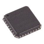
| 描述 | IC DAC 14BIT 210MSPS 32-LFCSP |
| 产品分类 | |
| 品牌 | Analog Devices Inc |
| 数据手册 | |
| 产品图片 |
|
| 产品型号 | AD9744ACPZRL7 |
| rohs | 无铅 / 符合限制有害物质指令(RoHS)规范要求 |
| 产品系列 | TxDAC® |
| 产品培训模块 | http://www.digikey.cn/PTM/IndividualPTM.page?site=cn&lang=zhs&ptm=19145http://www.digikey.cn/PTM/IndividualPTM.page?site=cn&lang=zhs&ptm=18614http://www.digikey.cn/PTM/IndividualPTM.page?site=cn&lang=zhs&ptm=26125http://www.digikey.cn/PTM/IndividualPTM.page?site=cn&lang=zhs&ptm=26140http://www.digikey.cn/PTM/IndividualPTM.page?site=cn&lang=zhs&ptm=26150http://www.digikey.cn/PTM/IndividualPTM.page?site=cn&lang=zhs&ptm=26147 |
| 位数 | 14 |
| 供应商器件封装 | 32-LFCSP-VQ(5x5) |
| 其它名称 | AD9744ACPZRL7DKR |
| 包装 | Digi-Reel® |
| 安装类型 | 表面贴装 |
| 封装/外壳 | 32-VFQFN 裸露焊盘,CSP |
| 工作温度 | -40°C ~ 85°C |
| 建立时间 | 11ns |
| 数据接口 | 并联 |
| 标准包装 | 1 |
| 电压源 | 模拟和数字 |
| 转换器数 | 1 |
| 输出数和类型 | 1 电流,单极1 电流,双极 |
| 采样率(每秒) | 210M |


- 商务部:美国ITC正式对集成电路等产品启动337调查
- 曝三星4nm工艺存在良率问题 高通将骁龙8 Gen1或转产台积电
- 太阳诱电将投资9.5亿元在常州建新厂生产MLCC 预计2023年完工
- 英特尔发布欧洲新工厂建设计划 深化IDM 2.0 战略
- 台积电先进制程称霸业界 有大客户加持明年业绩稳了
- 达到5530亿美元!SIA预计今年全球半导体销售额将创下新高
- 英特尔拟将自动驾驶子公司Mobileye上市 估值或超500亿美元
- 三星加码芯片和SET,合并消费电子和移动部门,撤换高东真等 CEO
- 三星电子宣布重大人事变动 还合并消费电子和移动部门
- 海关总署:前11个月进口集成电路产品价值2.52万亿元 增长14.8%


PDF Datasheet 数据手册内容提取
14-Bit, 210 MSPS TxDAC® D/A Converter Data Sheet AD9744 FEATURES APPLICATIONS High performance member of pin-compatible Wideband communication transmit channel TxDAC product family Direct IFs Excellent spurious-free dynamic range performance Base stations SFDR to Nyquist Wireless local loops 83 dBc at 5 MHz output Digital radio links 80 dBc at 10 MHz output Direct digital synthesis (DDS) 73 dBc at 20 MHz output Instrumentation SNR at 5 MHz output, 125 MSPS: 77 dB Twos complement or straight binary data format FUNCTIONAL BLOCK DIAGRAM Differential current outputs: 2 mA to 20 mA Power dissipation: 135 mW at 3.3 V 3.3V Power-down mode: 15 mW at 3.3 V On-chip 1.2 V reference REFLO 150pF AVDD ACOM 1.2V REF CMOS-compatible digital interface 0.1µF REFIO CURRENT AD9744 28-lead SOIC, 28-lead TSSOP, and 32-lead LFCSP packages FS ADJ SOURCE ARRAY Edge-triggered latches RSET 3.3V DVDD IOUTA SEGMENTED LSB DCOM SWITCHES SWITCHES IOUTB CLOCK CLOCK LATCHES MODE SLEEP DIGITAL DATA INPUTS (DB13–DB0) 02913-001 Figure 1. GENERAL DESCRIPTION The AD97441 is a 14-bit resolution, wideband, third generation Edge-triggered input latches and a 1.2 V temperature compensated member of the TxDAC series of high performance, low power band gap reference have been integrated to provide a complete CMOS digital-to-analog converters (DACs). The TxDAC family, monolithic DAC solution. The digital inputs support 3 V consisting of pin-compatible 8-, 10-, 12-, and 14-bit DACs, is CMOS logic families. specifically optimized for the transmit signal path of communi- PRODUCT HIGHLIGHTS cation systems. All of the devices share the same interface options, 1. The AD9744 is the 14-bit member of the pin compatible TxDAC small outline package, and pinout, providing an upward or family, which offers excellent INL and DNL performance. downward component selection path based on performance, 2. Data input supports twos complement or straight binary data resolution, and cost. The AD9744 offers exceptional ac and dc coding. performance while supporting update rates up to 210 MSPS. 3. High speed, single-ended CMOS clock input supports The AD9744’s low power dissipation makes it well suited for 210 MSPS conversion rate. portable and low power applications. Its power dissipation can 4. Low power: Complete CMOS DAC function operates on be further reduced to a mere 60 mW with a slight degradation 135 mW from a 2.7 V to 3.6 V single supply. The DAC full- in performance by lowering the full-scale current output. Also, scale current can be reduced for lower power operation, and a a power-down mode reduces the standby power dissipation to sleep mode is provided for low power idle periods. approximately 15 mW. A segmented current source architecture 5. On-chip voltage reference: The AD9744 includes a 1.2 V is combined with a proprietary switching technique to reduce temperature compensated band gap voltage reference. spurious components and enhance dynamic performance. 6. Industry-standard 28-lead SOIC, 28-lead TSSOP, and 32-lead LFCSP packages. 1Protected by U.S. Patent Numbers 5568145, 5689257, and 5703519. Rev. C Document Feedback Information furnished by Analog Devices is believed to be accurate and reliable. However, no responsibility is assumed by Analog Devices for its use, nor for any infringements of patents or other One Technology Way, P.O. Box 9106, Norwood, MA 02062-9106, U.S.A. rights of third parties that may result from its use. Specifications subject to change without notice. No license is granted by implication or otherwise under any patent or patent rights of Analog Devices. Tel: 781.329.4700 ©2003–2013 Analog Devices, Inc. All rights reserved. Trademarks and registered trademarks are the property of their respective owners. Technical Support www.analog.com
AD9744 Data Sheet TABLE OF CONTENTS Features .............................................................................................. 1 Reference Control Amplifier .................................................... 13 Applications ....................................................................................... 1 DAC Transfer Function ............................................................. 14 Functional Block Diagram .............................................................. 1 Analog Outputs .......................................................................... 14 General Description ......................................................................... 1 Digital Inputs .............................................................................. 15 Product Highlights ........................................................................... 1 Clock Input .................................................................................. 15 Revision History ............................................................................... 2 DAC Timing ................................................................................ 16 Specifications ..................................................................................... 3 Power Dissipation....................................................................... 16 DC Specifications ......................................................................... 3 Applying the AD9744 ................................................................ 17 Dynamic Specifications ............................................................... 4 Differential Coupling Using a Transformer ............................ 17 Digital Specifications ................................................................... 5 Differential Coupling Using an Op Amp ................................ 17 Absolute Maximum Ratings ............................................................ 6 Single-Ended Unbuffered Voltage Output .............................. 18 Thermal Characteristics .............................................................. 6 Single-Ended, Buffered Voltage Output Configuration ........ 18 ESD Caution .................................................................................. 6 Power and Grounding Considerations, Power Supply Pin Configurations and Function Descriptions ........................... 7 Rejection ...................................................................................... 18 Typical Performance Characteristics ............................................. 8 Evaluation Board ............................................................................ 20 Terminology .................................................................................... 12 General Description ................................................................... 20 Functional Description .................................................................. 13 Outline Dimensions ....................................................................... 30 Reference Operation .................................................................. 13 Ordering Guide ............................................................................... 31 REVISION HISTORY 12/13—Rev. B to Rev. C 5/03—Rev. 0 to Rev. A Added 32-Lead LFCSP Package ....................................... Universal Added Table 5; Renumbered Sequentially .................................... 6 Edits to Features ................................................................................. 1 Added Exposed Pad Note to Figure 4 and Table 6, Pin Edits to Product Highlights .............................................................. 1 Configurations and Function Descriptions Section .................... 7 Edits to DC Specifications ................................................................ 2 Moved Terminology Section ......................................................... 12 Edits to Dynamic Specifications ...................................................... 3 Updated Outline Dimensions ....................................................... 30 Edits to Digital Specifications .......................................................... 4 Changes to Ordering Guide .......................................................... 31 Edits to Absolute Maximum Ratings .............................................. 5 4/05—Rev. A to Rev. B Edits to Thermal Characteristics ..................................................... 5 Updated Format .................................................................. Universal Edits to Ordering Guide ................................................................... 5 Changes to General Description .................................................... 1 Edits to Pin Configuration ............................................................... 6 Changes to Product Highlights ....................................................... 1 Edits to Pin Function Descriptions ................................................. 6 Changes to DC Specifications ......................................................... 3 Edits to Figure 2 ................................................................................. 7 Changes to Dynamic Specifications ............................................... 4 Replaced TPCs 1, 4, 7, and 8 ............................................................ 8 Changes to Pin Function Description ........................................... 7 Edits to Figure 3 .............................................................................. 10 Changes to Figure 6 and Figure 9 ................................................... 9 Edits to Functional Description ................................................... 10 Inserted New Figure 10; Renumbered Sequentially .................... 9 Added Clock Input Section ........................................................... 12 Changes to Figure 12, Figure 13, Figure 14, and Figure 15 ...... 10 Added Figure 7 ............................................................................... 12 Changes to Figure 22 Caption ...................................................... 11 Edits to DAC Timing Section ....................................................... 12 Inserted New Figure 23; Renumbered Sequentially .................. 11 Edits to Sleep Mode Operation Section....................................... 13 Changes to Functional Description ............................................. 13 Edits to Power Dissipation Section .............................................. 13 Changes to Reference Operation Section .................................... 13 Renumbered Figures 8 to Figure 26 ............................................. 13 Added Figure 25; Renumbered Sequentially .............................. 13 Added Figure 11 ............................................................................. 13 Changes to Digital Inputs Section ................................................ 15 Added Figure 27 to Figure 35 ....................................................... 21 Changes to Figure 31 and Figure 32............................................. 16 Updated Outline Dimensions ....................................................... 26 Updated Outline Dimensions ....................................................... 30 Changes to Ordering Guide .......................................................... 31 Rev. C | Page 2 of 32
Data Sheet AD9744 SPECIFICATIONS DC SPECIFICATIONS T to T , AVDD = 3.3 V, DVDD = 3.3 V, CLKVDD = 3.3 V, I = 20 mA, unless otherwise noted. MIN MAX OUTFS Table 1. Parameter Min Typ Max Unit RESOLUTION 14 Bits DC ACCURACY1 Integral Linearity Error (INL) −5 ±0.8 +5 LSB Differential Nonlinearity (DNL) −3 ±0.5 +3 LSB ANALOG OUTPUT Offset Error −0.02 +0.02 % of FSR Gain Error (Without Internal Reference) −0.5 ±0.1 +0.5 % of FSR Gain Error (With Internal Reference) −0.5 ±0.1 +0.5 % of FSR Full-Scale Output Current2 2 20 mA Output Compliance Range −1 +1.25 V Output Resistance 100 kΩ Output Capacitance 5 pF REFERENCE OUTPUT Reference Voltage 1.14 1.20 1.26 V Reference Output Current3 100 nA REFERENCE INPUT Input Compliance Range 0.1 1.25 V Reference Input Resistance (External Reference) 7 kΩ Small Signal Bandwidth 0.5 MHz TEMPERATURE COEFFICIENTS Offset Drift 0 ppm of FSR/°C Gain Drift (Without Internal Reference) ±50 ppm of FSR/°C Gain Drift (With Internal Reference) ±100 ppm of FSR/°C Reference Voltage Drift ±50 ppm/°C POWER SUPPLY Supply Voltages AVDD 2.7 3.3 3.6 V DVDD 2.7 3.3 3.6 V CLKVDD 2.7 3.3 3.6 V Analog Supply Current (I ) 33 36 mA AVDD Digital Supply Current (I )4 8 9 mA DVDD Clock Supply Current (I ) 5 6 mA CLKVDD Supply Current Sleep Mode (I ) 5 6 mA AVDD Power Dissipation4 135 145 mW Power Dissipation5 145 mW Power Supply Rejection Ratio—AVDD6 −1 +1 % of FSR/V Power Supply Rejection Ratio—DVDD6 −0.04 +0.04 % of FSR/V OPERATING RANGE −40 +85 °C 1 Measured at IOUTA, driving a virtual ground. 2 Nominal full-scale current, IOUTFS, is 32 times the IREF current. 3 An external buffer amplifier with input bias current <100 nA should be used to drive any external load. 4 Measured at fCLOCK = 25 MSPS and fOUT = 1 MHz. 5 Measured as unbuffered voltage output with IOUTFS = 20 mA and 50 Ω RLOAD at IOUTA and IOUTB, fCLOCK = 100 MSPS and fOUT = 40 MHz. 6 ±5% power supply variation. Rev. C | Page 3 of 32
AD9744 Data Sheet DYNAMIC SPECIFICATIONS T to T , AVDD = 3.3 V, DVDD = 3.3 V, CLKVDD = 3.3 V, I = 20 mA, differential transformer coupled output, 50 Ω doubly MIN MAX OUTFS terminated, unless otherwise noted. Table 2. Parameter Min Typ Max Unit DYNAMIC PERFORMANCE Maximum Output Update Rate (f ) 210 MSPS CLOCK Output Settling Time (t ) (to 0.1%)1 11 ns ST Output Propagation Delay (t ) 1 ns PD Glitch Impulse 5 pV-s Output Rise Time (10% to 90%)1 2.5 ns Output Fall Time (10% to 90%)1 2.5 ns Output Noise (I = 20 mA)2 50 pA/√Hz OUTFS Output Noise (I = 2 mA)2 30 pA/√Hz OUTFS Noise Spectral Density3 −155 dBm/Hz AC LINEARITY Spurious-Free Dynamic Range to Nyquist f = 25 MSPS; f = 1.00 MHz CLOCK OUT 0 dBFS Output 77 90 dBc −6 dBFS Output 87 dBc −12 dBFS Output 82 dBc −18 dBFS Output 82 dBc f = 65 MSPS; f = 1.00 MHz 85 dBc CLOCK OUT f = 65 MSPS; f = 2.51 MHz 84 dBc CLOCK OUT f = 65 MSPS; f = 10 MHz 80 dBc CLOCK OUT f = 65 MSPS; f = 15 MHz 75 dBc CLOCK OUT f = 65 MSPS; f = 25 MHz 74 dBc CLOCK OUT f = 165 MSPS; f = 21 MHz 73 dBc CLOCK OUT f = 165 MSPS; f = 41 MHz 60 dBc CLOCK OUT f = 210 MSPS; f = 41 MHz 68 dBc CLOCK OUT f = 210 MSPS; f = 69 MHz 64 dBc CLOCK OUT Spurious-Free Dynamic Range Within a Window f = 25 MSPS; f = 1.00 MHz; 2 MHz Span 84 90 dBc CLOCK OUT f = 50 MSPS; f = 5.02 MHz; 2 MHz Span 90 dBc CLOCK OUT f = 65 MSPS; f = 5.03 MHz; 2.5 MHz Span 87 dBc CLOCK OUT f = 125 MSPS; f = 5.04 MHz; 4 MHz Span 87 dBc CLOCK OUT Total Harmonic Distortion f = 25 MSPS; f = 1.00 MHz −86 −77 dBc CLOCK OUT f = 50 MSPS; f = 2.00 MHz −77 dBc CLOCK OUT f = 65 MSPS; f = 2.00 MHz −77 dBc CLOCK OUT f = 125 MSPS; f = 2.00 MHz −77 dBc CLOCK OUT Signal-to-Noise Ratio f = 65 MSPS; f = 5 MHz; I = 20 mA 82 dB CLOCK OUT OUTFS f = 65 MSPS; f = 5 MHz; I = 5 mA 88 dB CLOCK OUT OUTFS f = 125 MSPS; f = 5 MHz; I = 20 mA 77 dB CLOCK OUT OUTFS f = 125 MSPS; f = 5 MHz; I = 5 mA 78 dB CLOCK OUT OUTFS f = 165 MSPS; f = 5 MHz; I = 20 mA 70 dB CLOCK OUT OUTFS f = 165 MSPS; f = 5 MHz; I = 5 mA 70 dB CLOCK OUT OUTFS f = 210 MSPS; f = 5 MHz; I = 20 mA 74 dB CLOCK OUT OUTFS f = 210 MSPS; f = 5 MHz; I = 5 mA 67 dB CLOCK OUT OUTFS Rev. C | Page 4 of 32
Data Sheet AD9744 Parameter Min Typ Max Unit Multitone Power Ratio (8 Tones at 400 kHz Spacing) f = 78 MSPS; f = 15.0 MHz to 18.2 MHz CLOCK OUT 0 dBFS Output 66 dBc −6 dBFS Output 68 dBc −12 dBFS Output 62 dBc −18 dBFS Output 61 dBc 1 Measured single-ended into 50 Ω load. 2 Output noise is measured with a full-scale output set to 20 mA with no conversion activity. It is a measure of the thermal noise only. 3 Noise spectral density is the average noise power normalized to a 1 Hz bandwidth, with the DAC converting and producing an output tone. DIGITAL SPECIFICATIONS T to T , AVDD = 3.3 V, DVDD = 3.3 V, CLKVDD = 3.3 V, I = 20 mA, unless otherwise noted. MIN MAX OUTFS Table 3. Parameter Min Typ Max Unit DIGITAL INPUTS1 Logic 1 Voltage 2.1 3 V Logic 0 Voltage 0 0.9 V Logic 1 Current −10 +10 µA Logic 0 Current −10 +10 µA Input Capacitance 5 pF Input Setup Time (t) 2.0 ns S Input Hold Time (t ) 1.5 ns H Latch Pulse Width (t ) 1.5 ns LPW CLK INPUTS2 Input Voltage Range 0 3 V Common-Mode Voltage 0.75 1.5 2.25 V Differential Voltage 0.5 1.5 V 1 Includes CLOCK pin on SOIC/TSSOP packages and CLK+ pin on LFCSP package in single-ended clock input mode. 2 Applicable to CLK+ and CLK– inputs when configured for differential or PECL clock input mode. DB0–DB13 tS tH CLOCK tLPW tPD tST IOUTA OR 0.1% IOUTB 0.1% 02913-002 Figure 2. Timing Diagram Rev. C | Page 5 of 32
AD9744 Data Sheet ABSOLUTE MAXIMUM RATINGS Stresses above those listed under Absolute Maximum Ratings Table 4. may cause permanent damage to the device. This is a stress With Parameter Respect to Min Max Unit rating only; functional operation of the device at these or any other conditions above those indicated in the operational AVDD ACOM −0.3 +3.9 V section of this specification is not implied. Exposure to absolute DVDD DCOM −0.3 +3.9 V maximum rating conditions for extended periods may affect CLKVDD CLKCOM −0.3 +3.9 V device reliability. ACOM DCOM −0.3 +0.3 V ACOM CLKCOM −0.3 +0.3 V THERMAL CHARACTERISTICS DCOM CLKCOM −0.3 +0.3 V Thermal impedance measurements were taken on a 4-layer AVDD DVDD −3.9 +3.9 V board in still air, in accordance with EIA/JESD51-7. AVDD CLKVDD −3.9 +3.9 V DVDD CLKVDD −3.9 +3.9 V Table 5. Thermal Resistance CLOCK, SLEEP DCOM −0.3 DVDD + 0.3 V Package Type θ Unit JA Digital Inputs, DCOM −0.3 DVDD + 0.3 V 28-Lead 300-Mil SOIC 55.9 °C/W MODE 28-Lead TSSOP 67.7 °C/W IOUTA, IOUTB ACOM −1.0 AVDD + 0.3 V 32-Lead LFCSP 32.5 °C/W REFIO, REFLO, FS ACOM −0.3 AVDD + 0.3 V ADJ CLK+, CLK−, CLKCOM −0.3 CLKVDD + V ESD CAUTION CMODE 0.3 Junction 150 °C Temperature Storage −65 +150 °C Temperature Lead Temperature 300 °C (10 sec) Rev. C | Page 6 of 32
Data Sheet AD9744 PIN CONFIGURATIONS AND FUNCTION DESCRIPTIONS B) (MSB) DB13 1 28 CLOCK MS DB12 2 27 DVDD 8910111213 (OMEEP BBBBBBCL DB11 3 26 DCOM DDDDDDDS 21098765 DB10 4 25 MODE 33322222 DB9 5 24 AVDD AD9744 DB7 1 24 FS ADJ DB8 6 23 RESERVED DB6 2 23 REFIO DB7 7 (NToOt Pto V SIEcaWle)22 IOUTA DVDD 3 AD9744 22 ACOM DB5 4 21 IOUTA DB6 8 21 IOUTB DB4 5 TOP VIEW 20 IOUTB (Not to Scale) DB5 9 20 ACOM DB3 6 19 ACOM DB2 7 18 AVDD DB4 10 19 NC DB1 8 17 AVDD DB3 11 18 FS ADJ (LSB) DDDBBB210 111N432C = NO CONNEC111765TRRSLEEEFFEILOOP 02913-003 NOTES (LSB) DB0910DCOMCLKVDD11CLK+12CLK–13CLKCOM14CMODE15MODE16 02913-004 1. CONNECT THE EXPOSED PAD THERMALLY TO A COPPER GROUND PLANE Figure 3. 28-Lead SOIC and TSSOP FOR ENHANCED ELECTRICAL AND THERMAL PERFORMANCE. Figure 4. 32-Lead LFCSP Table 6. Pin Function Descriptions SOIC/TSSOP LFCSP Pin No. Pin No. Mnemonic Description 1 27 DB13 Most Significant Data Bit (MSB). 2 to 13 28 to 32, DB12 to Data Bits 12 to 1. 1, 2, 4 to 8 DB1 14 9 DB0 Least Significant Data Bit (LSB). 15 25 SLEEP Power-Down Control Input. Active high. Contains active pull-down circuit; it may be left unterminated if not used. 16 N/A REFLO Reference Ground when Internal 1.2 V Reference Used. Connect to ACOM for both internal and external reference operation modes. 17 23 REFIO Reference Input/Output. Serves as reference input when using external reference. Serves as 1.2 V reference output when using internal reference. Requires 0.1 µF capacitor to ACOM when using internal reference. 18 24 FS ADJ Full-Scale Current Output Adjust. 19 N/A NC No Internal Connection. 20 19, 22 ACOM Analog Common. 21 20 IOUTB Complementary DAC Current Output. Full-scale current when all data bits are 0s. 22 21 IOUTA DAC Current Output. Full-scale current when all data bits are 1s. 23 N/A RESERVED Reserved. Do not connect to common or supply. 24 17, 18 AVDD Analog Supply Voltage (3.3 V). 25 16 MODE Selects Input Data Format. Connect to DCOM for straight binary, DVDD for twos complement. N/A 15 CMODE Clock Mode Selection. Connect to CLKCOM for single-ended clock receiver (drive CLK+ and float CLK−). Connect to CLKVDD for differential receiver. Float for PECL receiver (terminations on-chip). 26 10, 26 DCOM Digital Common. 27 3 DVDD Digital Supply Voltage (3.3 V). 28 N/A CLOCK Clock Input. Data latched on positive edge of clock. N/A 12 CLK+ Differential Clock Input. N/A 13 CLK− Differential Clock Input. N/A 11 CLKVDD Clock Supply Voltage (3.3 V). N/A 14 CLKCOM Clock Common. N/A EPAD EPAD Exposed Pad. Connect the exposed pad thermally to a copper ground plane for enhanced electrical and thermal performance. Rev. C | Page 7 of 32
AD9744 Data Sheet TYPICAL PERFORMANCE CHARACTERISTICS 95 95 210MSPS (LFCSP) 90 90 125MSPS –6dBFS (LFCSP) 85 85 165MSPS (LFCSP) 80 65MSPS 80 –12dBFS (LFCSP) Bc) 75 210MSPS Bc)75 d d R ( 70 R (70 D 165MSPS D F F S 65 S65 125MSPS (LFCSP) –12dBFS 60 60 0dBFS 0dBFS (LFCSP) 55 55 –6dBFS 50 50 45 45 1 fOUT1 (0MHz) 100 02913-006 0 10 20 fOUT3 (0MHz) 40 50 60 02913-007 Figure 5. SFDR vs. fOUT at 0 dBFS Figure 8. SFDR vs. fOUT at 165 MSPS 95 95 0dBFS (LFCSP) 90 90 85 85 –6dBFS (LFCSP) –6dBFS 80 80 –12dBFS (LFCSP) dBc) 75 0dBFS –12dBFS Bc) 75 DR ( 70 R (d 70 F D S 65 F 65 S 60 60 0dBFS 55 55 –12dBFS –6dBFS 50 50 450 5 10fOUT (MHz)15 20 25 02913-009 450 10 20 30 fOUT4 (0MHz) 50 60 70 80 02913-055 Figure 6. SFDR vs. fOUT at 65 MSPS Figure 9. SFDR vs. fOUT at 210 MSPS 95 95 90 90 20mA 85 85 80 80 SFDR (dBc) 677505 –6dBFS –12dBFS SFDR (dBc) 677505 105mmAA 60 0dBFS 60 55 55 50 50 450 5 10 15 f2O0UT (MH25z) 30 35 40 45 02913-012 450 5 10fOUT (MHz)15 20 25 02913-010 Figure 7. SFDR vs. fOUT at 125 MSPS Figure 10. SFDR vs. fOUT and IOUTFS at 65 MSPS and 0 dBFS Rev. C | Page 8 of 32
Data Sheet AD9744 95 95 90 90 65MSPS (8.3,10.3) 165MSPS (22.6, 24.6) 85 85 65MSPS 210MSPS (LFCSP) 80 80 DR (dBc) 7705 210MSPS R (dBc) 7705 210MSPS (29,31) 78MSPS (10.1, 12.1) F D 210MSPS (29,31) S 65 SF 65 LFCSP 165MSPS 125MSPS 125MSPS (16.9, 18.9) 60 60 55 55 50 50 45 45 –25 –20 –1A5OUT (dBFS–1)0 –5 0 02913-013 –25 –20 –1A5OUT (dBFS–1)0 –5 0 02913-014 Figure 11. Single-Tone SFDR vs. AOUT at fOUT = fCLOCK/11 Figure 14. Dual-Tone IMD vs. AOUT at fOUT = fCLOCK/7 95 1.5 90 165MSPS (LFCSP) 1.0 85 65MSPS 125MSPS (LFCSP) 80 0.5 Bc) 75 SB) R (d 70 R (L 0 D O F R S 65 R E –0.5 60 165MSPS 55 125MSPS –1.0 210MSPS (LFCSP) 50 210MSPS 45–25 –20 –1A5OUT (dBFS–1)0 –5 0 02913-008 –1.50 4096 C8O19D2E 12288 16384 02913-015 Figure 12. Single-Tone SFDR vs. AOUT at fOUT = fCLOCK/5 Figure 15. Typical INL 90 1.0 IOUTFS = 20mA LFCSP 85 0.8 IOUTFS = 20mA 0.6 80 IOUTFS = 10mA LFCSP 0.4 75 SNR (dB) 70 ROR (LSB) 0.20 65 IOUTFS = 10mA ER–0.2 –0.4 60 IOUTFS = 5mA IOUTFS = 5mA LFCSP –0.6 55 –0.8 500 30 60 fC9L0OCK (MS1P20S) 150 180 210 02913-011 –1.00 4096 C8O1D92E 12288 16384 02913-018 Figure 13. SNR vs. fCLOCK and IOUTFS at fOUT = 5 MHz and 0 dBFS Figure 16. Typical DNL Rev. C | Page 9 of 32
AD9744 Data Sheet 95 0 fCLOCK = 78MSPS 90 4MHz –10 fOUT1 = 15.0MHz 85 –20 fOUT2 = 15.4MHz fOUT3 = 15.8MHz 80 m) –30 fSOFUDTR4 == 1765.d2BMcHz R (dBc) 7705 19MHz UDE (dB ––5400 AMPLITUDE = 0dBFS FD NIT S 65 G –60 34MHz MA 60 –70 49MHz 55 –80 50 –90 45 –100 –40 –20 0TEMPERA20TURE (°C4)0 60 80 02913-020 1 6 11 FRE1Q6UENCY2 (1MHz) 26 31 36 02913-021 Figure 17. SFDR vs. Temperature at 165 MSPS, 0 dBFS Figure 20. Four-Tone SFDR 0 –20 –39.01dBm –10 fCLOCK = 78MSPS –30 29.38000000MHz fOUT = 15.0MHz CHPWR –19.26dBm ACP UP –64.98dB –20 SFDR = 79dBc –40 ACPLOW +0.55dB AMPLITUDE = 0dBFS ALT1 UP –66.26dB m) –30 m) –50 ALT1 LOW –64.23dB UDE (dB ––5400 UDE (dB ––7600 GNIT –60 GNIT –80 A A M M –70 –90 C0 C0 –80 –100 C12 C12 C11 C11 –90 –110 CU1 CU1 CU2 CU2 –1001 6 11 FRE1Q6UENCY2 (1MHz) 26 31 36 02913-016 –120CENTER 33.22 MHz FREQU3E MNHCzY (MHz) SPAN 30 MHz 02913-017 Figure 18. Single-Tone SFDR Figure 21. Two-Carrier UMTS Spectrum, fCLOCK = 122.88 MSPS (ACLR = 64 dB) LFCSP Package 0 –20 –10 ffCOLUOTC1 K= =1 57.80MMSHPzS –30 RVABETTSWE B=NW 3= 0 =80 d3kB0HkzHz –20 fOUT2 = 15.4MHz –40 AVG = 50 SFDR = 77dBc m) –30 AMPLITUDE = 0dBFS m) –50 B B d –40 d –60 E ( E ( UD –50 UD –70 T T GNI –60 GNI –80 A A M M –70 –90 –80 –100 –90 –110 –1001 6 11 FRE1Q6UENCY2 (1MHz) 26 31 36 02913-019 –F1R250E.Q0C0 OE0MNFFTHSEzERT 10M3HR.8zE4F0 MBWHz –7d4B.Lc6O2WE–Rd8B4.m12 –7Sd5BP.UAc04PNP 1E8R–Md8HB4z.m54 02913-056 Figure 19. Dual-Tone SFDR Figure 22. Single-Carrier UMTS Spectrum, fCLOCK = 61.44 MSPS (ACLR = 74 dB) LFCSP Package Rev. C | Page 10 of 32
Data Sheet AD9744 3.3V REFLO AVDD ACOM 150pF +1.2V REF AD9744 VREFIO REFIO PMOS 0.1µF IREF FS ADJ CURRENT SOURCE ARRAY RSET VDIFF = VOUTA– VOUTB 2kΩ 3.3V DVDD IOUTA IOUTA SEGMENTED SWITCHES LSB VOUTA DCOM FOR DB13–DB5 SWITCHES IOUTB IOUTB VOUTB RLOAD CLOCK RLOAD 50Ω CLOCK LATCHES MODE 50Ω SLEEP DIGITAL DATA INPUTS (DB13–DB0) 02913-022 Figure 23. Simplified Block Diagram (SOIC/TSSOP Packages) Rev. C | Page 11 of 32
AD9744 Data Sheet TERMINOLOGY Power Supply Rejection Linearity Error (Also Called Integral Nonlinearity or INL) The maximum change in the full-scale output as the supplies It is defined as the maximum deviation of the actual analog are varied from nominal to minimum and maximum specified output from the ideal output, determined by a straight line voltages. drawn from zero to full scale. Settling Time Differential Nonlinearity (or DNL) The time required for the output to reach and remain within a DNL is the measure of the variation in analog value, normalized specified error band about its final value, measured from the to full scale, associated with a 1 LSB change in digital input code. start of the output transition. Monotonicity Glitch Impulse A DAC is monotonic if the output either increases or remains Asymmetrical switching times in a DAC give rise to undesired constant as the digital input increases. output transients that are quantified by a glitch impulse. It is Offset Error specified as the net area of the glitch in pV-s. The deviation of the output current from the ideal of zero is Spurious-Free Dynamic Range called the offset error. For IOUTA, 0 mA output is expected The difference, in dB, between the rms amplitude of the output when the inputs are all 0s. For IOUTB, 0 mA output is expected signal and the peak spurious signal over the specified when all inputs are set to 1s. bandwidth. Gain Error Total Harmonic Distortion (THD) The difference between the actual and ideal output span. The THD is the ratio of the rms sum of the first six harmonic actual span is determined by the output when all inputs are set components to the rms value of the measured input signal. It is to 1s minus the output when all inputs are set to 0s. expressed as a percentage or in decibels (dB). Output Compliance Range Multitone Power Ratio The range of allowable voltage at the output of a current output The spurious-free dynamic range containing multiple carrier DAC. Operation beyond the maximum compliance limits may tones of equal amplitude. It is measured as the difference cause either output stage saturation or breakdown, resulting in between the rms amplitude of a carrier tone to the peak nonlinear performance. spurious signal in the region of a removed tone. Temperature Drift It is specified as the maximum change from the ambient (25°C) value to the value at either T or T . For offset and gain MIN MAX drift, the drift is reported in ppm of full-scale range (FSR) per °C. For reference drift, the drift is reported in ppm per °C. 3.3V REFLO AVDD ACOM 150pF 1.2V REF AD9744 0.1µF REFIO PMOS FS ADJ CURRENT SOURCE ARRAY MINI-CIRCUITS RSET T1-1T 2kΩ 3.3V DVDD RHODE & SCHWARZ IOUTA FSEA30 DCOM SEGMFOERN TDEBD1 3S–WDIBTC5HES SWILTSCBHES IOUTB SAPNEACLTYRZEURM CLOCK MODE DDCVODMD 50Ω SLEEP LATCHES 50Ω RETIMED 50Ω CLOCK DIGITAL OUTPUT* DATA CLOCK *AWG2021 CLOCK RETIMED PULLSEEC GROENYE 9R2A10TOR OUTPUT TEKWTRITOHN OIXP TAIWOGN -42021 STOROFA 5TN0HS%AI TTDI OTUHNTEYS DCOIYNGC IFTLAAELL CL DLINAOGTC AEKD.GE 02913-005 Figure 24. Basic AC Characterization Test Set-Up (SOIC/TSSOP Packages) Rev. C | Page 12 of 32
Data Sheet AD9744 FUNCTIONAL DESCRIPTION Figure 23 shows a simplified block diagram of the AD9744. The current of less than 100 nA should be used. An example of the AD9744 consists of a DAC, digital control logic, and full-scale use of the internal reference is shown in Figure 26. output current control. The DAC contains a PMOS current AVDD source array capable of providing up to 20 mA of full-scale 84µA current (I ). The array is divided into 31 equal currents that OUTFS make up the five most significant bits (MSBs). The next four REFIO bits, or middle bits, consist of 15 equal current sources whose 7kΩ value is 1/16th of an MSB current source. The remaining LSBs are binary weighted fractions of the middle bits current sources. Iinmspteleamd oenf tainn gR t-h2eR m laiddddeler, aenndh alonwceesr ibtsit ds ywniathm cicu rpreernfto rsmouarnccees, REFLO 02913-057 for multitone or low amplitude signals and helps maintain the Figure 25. Equivalent Circuit of Internal Reference DAC’s high output impedance (that is, >100 kΩ). 3.3V All of these current sources are switched to one or the other of OPTIONAL the two output nodes, that is, IOUTA or IOUTB, via PMOS EXTERNAL REF BUFFER REFLO 150pF AVDD differential current switches. The switches are based on the +1.2V REF architecture that was pioneered in the AD9764 family, with REFIO fsuwritthcherin rge ftirnaenmsieenntts. Ttoh ries dsuwcietc dhi satrocrhtiitoenc tcuorne tarlisbou treedd ubcye tsh e ADDITILOONAADL 0.1µF FS ADJ CSAUORRURRRAECYNET vdarrivioeu ssig tnimalisn tgo etrhreo rins pauntds porf otvhied desif mferaetcnhtiianlg c cuorrmenptle smweitncthaersy. 2kΩ AD9744 02913-023 Figure 26. Internal Reference Configuration The analog and digital sections of the AD9744 have separate An external reference can be applied to REFIO, as shown in power supply inputs, that is, AVDD and DVDD, that can operate Figure 27. The external reference may provide either a fixed independently over a 2.7 V to 3.6 V range. The digital section, reference voltage to enhance accuracy and drift performance or which is capable of operating at a rate of up to 210 MSPS, a varying reference voltage for gain control. Note that the 0.1 µF consists of edge-triggered latches and segment decoding logic compensation capacitor is not required since the internal reference circuitry. The analog section includes the PMOS current is overridden, and the relatively high input impedance of REFIO sources, the associated differential switches, a 1.2 V band gap minimizes any loading of the external reference. voltage reference, and a reference control amplifier. 3.3V The DAC full-scale output current is regulated by the reference control amplifier and can be set from 2 mA to 20 mA via an REFLO AVDD external resistor, RSET, connected to the full-scale adjust AVDD 150pF +1.2V REF (FS ADJ) pin. The external resistor, in combination with both the reference control amplifier and voltage reference VREFIO, sets EXTERNAL VREFIO REFIO CURRENT the reference current I , which is replicated to the segmented REF FS ADJ SOURCE REF ARRAY current sources with the proper scaling factor. The full-scale RSET IREF = cRuErFreEnRt, EIONUTCFSE, iOs 3P2E tRimAeTs IIOREFN. VREFIO/RSET AD9744 RCAEOMFNPETLRRIFEOIENLRCE 02913-024 Figure 27. External Reference Configuration The AD9744 contains an internal 1.2 V band gap reference. The internal reference cannot be disabled, but can be easily overridden REFERENCE CONTROL AMPLIFIER by an external reference with no effect on performance. Figure 25 The AD9744 contains a control amplifier that is used to regulate shows an equivalent circuit of the band gap reference. REFIO the full-scale output current, I . The control amplifier is OUTFS serves as either an output or an input depending on whether the configured as a V-I converter, as shown in Figure 26, so that its internal or an external reference is used. To use the internal current output, I , is determined by the ratio of the V and REF REFIO reference, simply decouple the REFIO pin to ACOM with a an external resistor, R , as stated in Equation 4. I is copied SET REF 0.1 µF capacitor and connect REFLO to ACOM via a resistance to the segmented current sources with the proper scale factor to less than 5 Ω. The internal reference voltage will be present at set I , as stated in Equation 3. OUTFS REFIO. If the voltage at REFIO is to be used anywhere else in the circuit, an external buffer amplifier with an input bias Rev. C | Page 13 of 32
AD9744 Data Sheet The control amplifier allows a wide (10:1) adjustment span of Equation 7 and Equation 8 highlight some of the advantages of I over a 2 mA to 20 mA range by setting I between 62.5 µA operating the AD9744 differentially. First, the differential operation OUTFS REF and 625 µA. The wide adjustment span of I provides several helps cancel common-mode error sources associated with IOUTA OUTFS benefits. The first relates directly to the power dissipation of the and IOUTB, such as noise, distortion, and dc offsets. Second, the AD9744, which is proportional to I (refer to the Power differential code dependent current and subsequent voltage, V , OUTFS DIFF Dissipation section). The second relates to the 20 dB adjustment, is twice the value of the single-ended voltage output (that is, V OUTA which is useful for system gain control purposes. or V ), thus providing twice the signal power to the load. OUTB The small signal bandwidth of the reference control amplifier is Note that the gain drift temperature performance for a single- approximately 500 kHz and can be used for low frequency small ended (V and V ) or differential output (V ) of the OUTA OUTB DIFF signal multiplying applications. AD9744 can be enhanced by selecting temperature tracking DAC TRANSFER FUNCTION resistors for RLOAD and RSET due to their ratiometric relationship, as shown in Equation 8. Both DACs in the AD9744 provide complementary current ANALOG OUTPUTS outputs, IOUTA and IOUTB. IOUTA provides a near full-scale current output, I , when all bits are high (that is, DAC The complementary current outputs in each DAC, IOUTA, and OUTFS CODE = 16383), while IOUTB, the complementary output, IOUTB may be configured for single-ended or differential oper- provides no current. The current output appearing at IOUTA ation. IOUTA and IOUTB can be converted into complementary and IOUTB is a function of both the input code and I and single-ended voltage outputs, V and V , via a load resistor, OUTFS OUTA OUTB can be expressed as R , as described in the DAC Transfer Function section by LOAD ( ) Equation 5 through Equation 8. The differential voltage, V , IOUTA= DACCODE/16384 ×I (1) DIFF OUTFS existing between V and V , can also be converted to a ( ) OUTA OUTB IOUTB= 16383−DACCODE/16384×I (2) single-ended voltage via a transformer or differential amplifier OUTFS configuration. The ac performance of the AD9744 is optimum where DAC CODE = 0 to 16383 (that is, decimal representation). and specified using a differential transformer-coupled output in As mentioned previously, IOUTFS is a function of the reference which the voltage swing at IOUTA and IOUTB is limited to ±0.5 V. current I , which is nominally set by a reference voltage, REF The distortion and noise performance of the AD9744 can be V , and external resistor, R . It can be expressed as REFIO SET enhanced when it is configured for differential operation. The IOUTFS =32×IREF (3) common-mode error sources of both IOUTA and IOUTB can be significantly reduced by the common-mode rejection of a where transformer or differential amplifier. These common-mode I =V /R (4) REF REFIO SET error sources include even-order distortion products and noise. The two current outputs will typically drive a resistive load The enhancement in distortion performance becomes more directly or via a transformer. If dc coupling is required, IOUTA significant as the frequency content of the reconstructed and IOUTB should be directly connected to matching resistive waveform increases and/or its amplitude decreases. This is due loads, R , that are tied to analog common, ACOM. Note that to the first-order cancellation of various dynamic common- LOAD R may represent the equivalent load resistance seen by mode distortion mechanisms, digital feedthrough, and noise. LOAD IOUTA or IOUTB as would be the case in a doubly terminated Performing a differential-to-single-ended conversion via a 50 Ω or 75 Ω cable. The single-ended voltage output appearing transformer also provides the ability to deliver twice the at the IOUTA and IOUTB nodes is simply reconstructed signal power to the load (assuming no source V =IOUTA×R (5) termination). Since the output currents of IOUTA and IOUTB OUTA LOAD are complementary, they become additive when processed V =IOUTB×R (6) OUTB LOAD differentially. A properly selected transformer will allow the Note that the full-scale value of V and V should not AD9744 to provide the required power and voltage levels to OUTA OUTB exceed the specified output compliance range to maintain different loads. specified distortion and linearity performance. The output impedance of IOUTA and IOUTB is determined by V =(IOUTA−IOUTB)×R (7) the equivalent parallel combination of the PMOS switches DIFF LOAD associated with the current sources and is typically 100 kΩ in Substituting the values of IOUTA, IOUTB, I , and V can be REF DIFF parallel with 5 pF. It is also slightly dependent on the output expressed as voltage (that is, V and V ) due to the nature of a PMOS [( ) ] OUTA OUTB V = 2×DACCODE−16383 /16384 device. As a result, maintaining IOUTA and/or IOUTB at a (32DI×FFR /R )×V (8) virtual ground via an I-V op amp configuration will result in LOAD SET REFIO the optimum dc linearity. Note that the INL/DNL specifications Rev. C | Page 14 of 32
Data Sheet AD9744 for the AD9744 are measured with IOUTA maintained at a CLOCK INPUT virtual ground via an op amp. SOIC/TSSOP Packages IOUTA and IOUTB also have a negative and positive voltage The 28-lead package options have a single-ended clock input compliance range that must be adhered to in order to achieve (CLOCK) that must be driven to rail-to-rail CMOS levels. The optimum performance. The negative output compliance range quality of the DAC output is directly related to the clock quality, of −1 V is set by the breakdown limits of the CMOS process. and jitter is a key concern. Any noise or jitter in the clock will Operation beyond this maximum limit may result in a breakdown translate directly into the DAC output. Optimal performance of the output stage and affect the reliability of the AD9744. will be achieved if the CLOCK input has a sharp rising edge, The positive output compliance range is slightly dependent on since the DAC latches are positive edge triggered. the full-scale output current, IOUTFS. It degrades slightly from its LFCSP Package nominal 1.2 V for an I = 20 mA to 1 V for an I = 2 mA. OUTFS OUTFS A configurable clock input is available in the LFCSP package, The optimum distortion performance for a single-ended or which allows for one single-ended and two differential modes. differential output is achieved when the maximum full-scale The mode selection is controlled by the CMODE input, as signal at IOUTA and IOUTB does not exceed 0.5 V. summarized in Table 7. Connecting CMODE to CLKCOM DIGITAL INPUTS selects the single-ended clock input. In this mode, the CLK+ The AD9744 digital section consists of 14 input bit channels input is driven with rail-to-rail swings and the CLK– input is and a clock input. The 14-bit parallel data inputs follow left floating. If CMODE is connected to CLKVDD, the differential standard positive binary coding, where DB13 is the most receiver mode is selected. In this mode, both inputs are high significant bit (MSB) and DB0 is the least significant bit (LSB). impedance. The final mode is selected by floating CMODE. This IOUTA produces a full-scale output current when all data bits mode is also differential, but internal terminations for positive are at Logic 1. IOUTB produces a complementary output with emitter-coupled logic (PECL) are activated. There is no significant the full-scale current split between the two outputs as a performance difference among any of the three clock input modes. function of the input code. Table 7. Clock Mode Selection DVDD CMODE Pin Clock Input Mode CLKCOM Single-Ended CLKVDD Differential DIGITAL INPUT Float PECL 02913-025 TChLeO sCinKg lien-peuntd iend t ihnep 2u8t -mleoadde p oapckeraagteess, ians tphree vsiaomusel yw daye sacsr itbheed . Figure 28. Equivalent Digital Input In the differential input mode, the clock input functions as a The digital interface is implemented using an edge-triggered high impedance differential pair. The common-mode level of master/slave latch. The DAC output updates on the rising edge the CLK+ and CLK− inputs can vary from 0.75 V to 2.25 V, and of the clock and is designed to support a clock rate as high as the differential voltage can be as low as 0.5 V p-p. This mode 210 MSPS. The clock can be operated at any duty cycle that can be used to drive the clock with a differential sine wave since meets the specified latch pulse width. The setup and hold the high gain bandwidth of the differential inputs will convert times can also be varied within the clock cycle as long as the the sine wave into a single-ended square wave internally. specified minimum times are met, although the location of The final clock mode allows for a reduced external component these transition edges may affect digital feedthrough and count when the DAC clock is distributed on the board using distortion performance. Best performance is typically achieved PECL logic. The internal termination configuration is shown in when the input data transitions on the falling edge of a 50% Figure 29. These termination resistors are untrimmed and can duty cycle clock. vary up to ±20%. However, matching between the resistors should generally be better than ±1%. Rev. C | Page 15 of 32
AD9744 Data Sheet POWER DISSIPATION AD9744 CLK+ The power dissipation, P , of the AD9744 is dependent on D CLOCK CLK– RECEIVER TO DAC CORE several factors that include: 50Ω 50Ω • The power supply voltages (AVDD, CLKVDD, and DVDD) VTT = 1.3V NOM 02913-026 • The full-scale current output IOUTFS Figure 29. Clock Termination in PECL Mode • The update rate fCLOCK • The reconstructed digital input waveform DAC TIMING The power dissipation is directly proportional to the analog supply Input Clock and Data Timing Relationship current, I , and the digital supply current, I . I is AVDD DVDD AVDD Dynamic performance in a DAC is dependent on the relationship directly proportional to I , as shown in Figure 31, and is OUTFS between the position of the clock edges and the time at which insensitive to f . Conversely, I is dependent on both the CLOCK DVDD the input data changes. The AD9744 is rising edge triggered, digital input waveform, f , and digital supply DVDD. Figure 32 CLOCK and so exhibits dynamic performance sensitivity when the data shows I as a function of full-scale sine wave output ratios DVDD transition is close to this edge. In general, the goal when applying (f /f ) for various update rates with DVDD = 3.3 V. OUT CLOCK the AD9744 is to make the data transition close to the falling 35 clock edge. This becomes more important as the sample rate increases. Figure 30 shows the relationship of SFDR to clock 30 placement with different sample rates. Note that at the lower sample rates, more tolerance is allowed in clock placement, 25 while at higher rates, more care must be taken. A) m 75 (D20 D V A 70 I 15 65 60 20MHz SFDR 10 B d5505 50MHz SFDR 02 4 6 8 IO1U0TFS (m12A) 14 16 18 20 02913-028 45 Figure 31. IAVDD vs. IOUTFS 20 40 50MHz SFDR 18 35–3 –2 –1 n0s 1 2 3 02913-027 16 210MSPS 14 165MSPS Figure 30. SFDR vs. Clock Placement at fOUT = 20 MHz and 50 MHz A)12 m Sleep Mode Operation (D10 125MSPS D V The AD9744 has a power-down function that turns off the output ID 8 current and reduces the supply current to less than 6 mA over 6 65MSPS the specified supply range of 2.7 V to 3.6 V and temperature 4 range. This mode can be activated by applying a logic level 1 to 2 the SLEEP pin. The SLEEP pin logic threshold is equal to 0.5 Ω 0 AciVrcDuiDt .t hTahti se ndsiugriteasl tihnaptu tth ael sAoD co97n4ta4i nres mana iancst ievnea pbuleldl- difo twhnis 0.01 RATIO (f0O.U1T/fCLOCK) 1 02913-029 input is left disconnected. The AD9744 takes less than 50 ns to Figure 32. IDVDD vs. Ratio at DVDD = 3.3 V power down and approximately 5 µs to power back up. Rev. C | Page 16 of 32
Data Sheet AD9744 11 for impedance matching purposes. Note that the transformer 10 provides ac coupling only. 9 MINI-CIRCUITS T1-1T 8 IOUTA 22 mA)7 DIFF AD9744 RLOAD (D6 PECL ICLKVD45 IOUTB 21 OPTIONALRDIFF 02913-031 SE Figure 34. Differential Output Using a Transformer 3 The center tap on the primary side of the transformer must be 2 connected to ACOM to provide the necessary dc current path 1 for both IOUTA and IOUTB. The complementary voltages 00 50 1f0C0LOCK (MSP1S50) 200 250 02913-030 sawppinegar siynmg mat eItOriUcaTlAly aanrodu InOdU ATCBO (Mth aatn ids, sVhOoUuTlAd a bned m VaOiUnTtBa)i ned Figure 33. ICLKVDD vs. fCLOCK and Clock Mode with the specified output compliance range of the AD9744. A APPLYING THE AD9744 differential resistor, R , may be inserted in applications where DIFF Output Configurations the output of the transformer is connected to the load, RLOAD, via a passive reconstruction filter or cable. R is determined DIFF The following sections illustrate some typical output configurations by the transformer’s impedance ratio and provides the proper for the AD9744. Unless otherwise noted, it is assumed that I OUTFS source termination that results in a low VSWR. Note that approx- is set to a nominal 20 mA. For applications requiring the optimum imately half the signal power will be dissipated across R . DIFF dynamic performance, a differential output configuration is DIFFERENTIAL COUPLING USING AN OP AMP suggested. A differential output configuration may consist of either an RF transformer or a differential op amp configuration. An op amp can also be used to perform a differential-to-single- The transformer configuration provides the optimum high ended conversion, as shown in Figure 35. The AD9744 is frequency performance and is recommended for any application configured with two equal load resistors, R , of 25 Ω. The LOAD that allows ac coupling. The differential op amp configuration is differential voltage developed across IOUTA and IOUTB is suitable for applications requiring dc coupling, a bipolar output, converted to a single-ended signal via the differential op amp signal gain, and/or level shifting within the bandwidth of the configuration. An optional capacitor can be installed across chosen op amp. IOUTA and IOUTB, forming a real pole in a low-pass filter. The A single-ended output is suitable for applications requiring a addition of this capacitor also enhances the op amp’s distortion unipolar voltage output. A positive unipolar output voltage performance by preventing the DAC’s high slewing output from results if IOUTA and/or IOUTB are connected to an appro- overloading the op amp’s input. priately sized load resistor, RLOAD, referred to ACOM. This 500 configuration may be more suitable for a single-supply system AD9744 225 requiring a dc-coupled, ground referred output voltage. Alter- IOUTA 22 natively, an amplifier could be configured as an I-V converter, AD8047 225 thus converting IOUTA or IOUTB into a negative unipolar IOUTB 21 COPT voltage. This configuration provides the best dc linearity since 500 IDOIUFFTAER oEr NIOTUIATBL iCs OmUaiPntLaIinNeGd aUt Sa IvNirGtu aAl ground. 25 25 02913-032 Figure 35. DC Differential Coupling Using an Op Amp TRANSFORMER The common-mode rejection of this configuration is typically An RF transformer can be used to perform a differential-to-single- determined by the resistor matching. In this circuit, the differential ended signal conversion, as shown in Figure 34. A differentially op amp circuit using the AD8047 is configured to provide some coupled transformer output provides the optimum distortion additional signal gain. The op amp must operate off a dual supply performance for output signals whose spectral content lies since its output is approximately ±1 V. A high speed amplifier within the transformer’s pass band. An RF transformer, such as capable of preserving the differential performance of the AD9744 the Mini-Circuits T1–1T, provides excellent rejection of while meeting other system level objectives (such as cost or common-mode distortion (that is, even-order harmonics) and power) should be selected. The op amp’s differential gain, gain noise over a wide frequency range. It also provides electrical setting resistor values, and full-scale output swing capabilities isolation and the ability to deliver twice the power to the load. should all be considered when optimizing this circuit. Transformers with different impedance ratios may also be used Rev. C | Page 17 of 32
AD9744 Data Sheet The differential circuit shown in Figure 36 provides the necessary COPT level shifting required in a single-supply system. In this case, RFB AVDD, which is the positive analog supply for both the AD9744 200Ω and the op amp, is also used to level-shift the differential output AD9744 IOUTFS=10mA of the AD9744 to midsupply (that is, AVDD/2). The AD8041 is IOUTA 22 a suitable op amp for this application. U1 VOUT= IOUTFS× RFB IOUTB 21 AD9744 225Ω 500Ω 200Ω 02913-035 IOUTA 22 Figure 38. Unipolar Buffered Voltage Output AD8041 225Ω POWER AND GROUNDING CONSIDERATIONS, IOUTB 21 COPT 1kΩ POWER SUPPLY REJECTION AVDD 25Ω 25Ω 1kΩ 02913-033 Mlesasn tyh aanp pidliecaalt ioopnesr asteienkg hcoignhd sitpioeneds. aInnd t hheisgeh a ppeprlifcoartmioann ccier cuunitdse, r Figure 36. Single-Supply DC Differential Coupled Circuit the implementation and construction of the printed circuit SINGLE-ENDED UNBUFFERED VOLTAGE OUTPUT board is as important as the circuit design. Proper RF techniques must be used for device selection, placement, and routing as Figure 37 shows the AD9744 configured to provide a unipolar well as power supply bypassing and grounding to ensure output range of approximately 0 V to 0.5 V for a doubly terminated optimum performance. Figure 43 to Figure 46 illustrate the 50 Ω cable since the nominal full-scale current, I , of 20 mA OUTFS recommended printed circuit board ground, power, and signal flows through the equivalent R of 25 Ω. In this case, R LOAD LOAD plane layouts implemented on the AD9744 evaluation board. represents the equivalent load resistance seen by IOUTA or IOUTB. The unused output (IOUTA or IOUTB) can be connected One factor that can measurably affect system performance is to ACOM directly or via a matching R . Different values of the ability of the DAC output to reject dc variations or ac noise LOAD I and R can be selected as long as the positive compliance superimposed on the analog or digital dc power distribution. OUTFS LOAD range is adhered to. One additional consideration in this mode This is referred to as the power supply rejection ratio (PSRR). is the integral nonlinearity (INL), discussed in the Analog For dc variations of the power supply, the resulting performance Outputs section. For optimum INL performance, the single- of the DAC directly corresponds to a gain error associated with ended, buffered voltage output configuration is suggested. the DAC’s full-scale current, IOUTFS. AC noise on the dc supplies is common in applications where the power distribution is AD9744 IOUTFS=20mA generated by a switching power supply. Typically, switching VOUTA=0VTO0.5V IOUTA 22 power supply noise will occur over the spectrum from tens of 50Ω 50Ω kHz to several MHz. The PSRR vs. frequency of the AD9744 IOUTB 21 25Ω 02913-034 AVDD85 supply over this frequency range is shown in Figure 39. Figure 37. 0 V to 0.5 V Unbuffered Voltage Output 80 SINGLE-ENDED, BUFFERED VOLTAGE OUTPUT 75 CONFIGURATION 70 Figure 38 shows a buffered single-ended output configuration B) d65 in which the op amp U1 performs an I-V conversion on the R ( R S60 AD9744 output current. U1 maintains IOUTA (or IOUTB) at a P virtual ground, minimizing the nonlinear output impedance 55 effect on the DAC’s INL performance as described in the Analog 50 Outputs section. Although this single-ended configuration 45 typically provides the best dc linearity performance, its ac dlimistioterdti obny pUe1r’fso srlmewa nrcaete a ct ahpiagbhielirt iDesA. CU 1u ppdroatvei dreaste as nmeagya tbivee 400 2 4FREQUEN6CY (MHz)8 10 12 02913-036 unipolar output voltage, and its full-scale output voltage is Figure 39. Power Supply Rejection Ratio (PSRR) vs. Frequency simply the product of R and I . The full-scale output FB OUTFS Note that the ratio in Figure 39 is calculated as amps out/volts should be set within U1’s voltage output swing capabilities by in. Noise on the analog power supply has the effect of modulating scaling I and/or R . An improvement in ac distortion OUTFS FB the internal switches, and therefore the output current. The performance may result with a reduced I since the signal OUTFS voltage noise on AVDD, therefore, will be added in a nonlinear current U1 will be required to sink less signal current. manner to the desired IOUT. Due to the relative different size of Rev. C | Page 18 of 32
Data Sheet AD9744 these switches, the PSRR is very code dependent. This can produce AD9744 features separate analog and digital supplies and a mixing effect that can modulate low frequency power supply ground pins to optimize the management of analog and digital noise to higher frequencies. Worst-case PSRR for either one of ground currents in a system. In general, AVDD, the analog the differential DAC outputs will occur when the full-scale current supply, should be decoupled to ACOM, the analog common, as is directed toward that output. As a result, the PSRR measurement close to the chip as physically possible. Similarly, DVDD, the in Figure 39 represents a worst-case condition in which the digital supply, should be decoupled to DCOM as close to the digital inputs remain static and the full-scale output current of chip as physically possible. 20 mA is directed to the DAC output being measured. For those applications that require a single 3.3 V supply for both An example serves to illustrate the effect of supply noise on the the analog and digital supplies, a clean analog supply may be analog supply. Suppose a switching regulator with a switching generated using the circuit shown in Figure 40. The circuit frequency of 250 kHz produces 10 mV of noise and, for consists of a differential LC filter with separate power supply simplicity’s sake (ignoring harmonics), all of this noise is and return lines. Lower noise can be attained by using low ESR concentrated at 250 kHz. To calculate how much of this type electrolytic and tantalum capacitors. undesired noise will appear as current noise superimposed on FERRITE BEADS the DAC’s full-scale current, I , one must determine the OUTFS TTL/CMOS AVDD PSRR in dB using Figure 39 at 250 kHz. To calculate the PSRR LOGIC 100µF 10µF–22µF 0.1µF CIRCUITS ELECT. TANT. CER. for a given R , such that the units of PSRR are converted LOAD ACOM from A/V to V/V, adjust the curve in Figure 39 by the scaling factor 20 Ω log (R ). For instance, if R is 50 Ω, the PSRR LOAD LOAD iws hreicdhu icse 8d5 b dyB 3 4in d FBi g(tuhraet 3 i9s,, PbSeRcoRm oefs t 5h1e dDBA VCO aUtT 2/V50IN k).H z, POWE3R. 3SVUPPLY 02913-037 Figure 40. Differential LC Filter for Single 3.3 V Applications Proper grounding and decoupling should be a primary objective in any high speed, high resolution system. The Rev. C | Page 19 of 32
AD9744 Data Sheet EVALUATION BOARD GENERAL DESCRIPTION This board allows the user the flexibility to operate the AD9744 in various configurations. Possible output configurations include The TxDAC family evaluation boards allow for easy setup and transformer coupled, resistor terminated, and single and testing of any TxDAC product in the SOIC and LFCSP packages. differential outputs. The digital inputs are designed to be driven Careful attention to layout and circuit design, combined with a from various word generators, with the on-board option to add prototyping area, allows the user to evaluate the AD9744 easily a resistor network for proper load termination. Provisions are and effectively in any application where high resolution, high also made to operate the AD9744 with either the internal or speed conversion is required. external reference or to exercise the power-down feature. J1 2 1 DB13X 4 3 DB12X 6 5 DB11X M M 8 7 O O 10 9 DB10X DCR1R2R3R4R5R6R7R8R9 ORPPT5 DC R1R2R3R4R5R6R7R8R9 ORPPT1 12 11 DDBB98XX 12345678910 12345678910 1112222233333446802468024680 1111222223333335791357913579 JP3 CDDDDDDDDKBBBBBBBBE76543210XXXXXXXXXTX DDDDDDDDDDDDDDBBBBBBBBBBBBBB111132109876543210XXXXXXXXXXXXXX 12345678123456RRRRRRRRRRRRRRPPPPPPPPPPPPPP33333333444444 2222222222222222222222222222ΩΩΩΩΩΩΩΩΩΩΩΩΩΩ111119111111114321065432165 DDDDDDDDDDDDDDBBBBBBBBBBBBBB111198765432103210 7RP4 22Ω10 RIBBON CKEXTX 8RP4 22Ω9 CKEXT 1 234567890 1234567890 L2 BEAD REDTP2 DCOMR1R2R3R4R5R6R7R8R91 ORPPT6 DCOMR12RR3R4R5R6R7R8R91 ORPPT2 TB1 1 DVDD +C4 C7 10µF C6 0.1µF BLK 25V 0.1µF BLK BLK TP4 TP7 TP8 TB1 2 RED L3 BEAD TP5 TB1 3 AVDD +C5 C9 10µF C8 TB1 4 0.1µF BLKTP6 25V 0.1µF BLKTP10 BLKTP9 02913-038 Figure 41. SOIC Evaluation Board—Power Supply and Digital Inputs Rev. C | Page 20 of 32
Data Sheet AD9744 AVDD CUT +C14 C16 C17 UNDER DUT 10µF 0.1µF 0.1µF 16V JP6 DVDD +C15 C18 C19 DVDD JP10 1106VµF 0.1µF 0.1µF R5 IX 1 A2 B 3 OPT S2 CLOCK IOUTA R11 50Ω CKEXT S5 JP4 CLOCK DVDD TP1 R4 WHT 50Ω DDBB1132 12 DDBB1132 CDLOVDCDK 2287 DVDD R102kΩ OCP13T JP8 DB11 3 DB11 DCOM 26 JP2 IOUT DB10 4 DB10 MODE 25 DB9 5 DB9 AVDD 24 AVDD MODE 3 T1 4 DB8 6 DB8 RESERVED 23 DDBB76 78 DDBB76 ADU91742 IIOOUUTTAB 2221 ORPT6 2 5 S3 DB5 9 DB5 ACOM 20 1 6 DB4 10 DB4 NC 19 T1-1T DB3 11 DB3 FS ADJ 18 REF TP3 DDBB21 1123 DDBB21 RREEFFLIOO 1176 WHT C0.11µF C0.21µF C12 JP9 DB0 14 DB0 SLEEP 15 R1 C0.111µF AVDD OPT 2kΩ 2 AVDD 1 A B 3 SLEEP S1 5R01Ω0 EXT JP5 INT TP11 IOUTB WHT REF R103kΩ IY 1 AJ2P1B1 3 02913-039 Figure 42. SOIC Evaluation Board—Output Signal Conditioning Rev. C | Page 21 of 32
AD9744 Data Sheet 02913-040 Figure 43. SOIC Evaluation Board—Primary Side 02913-041 Figure 44. SOIC Evaluation Board—Secondary Side Rev. C | Page 22 of 32
Data Sheet AD9744 02913-042 Figure 45. SOIC Evaluation Board—Ground Plane 02913-043 Figure 46. SOIC Evaluation Board—Power Plane Rev. C | Page 23 of 32
AD9744 Data Sheet 02913-044 Figure 47. SOIC Evaluation Board Assembly—Primary Side 02913-045 Figure 48. SOIC Evaluation Board Assembly—Secondary Side Rev. C | Page 24 of 32
Data Sheet AD9744 RED L1BEAD TP12 TB1 1 CVDD 2 1 DB13X 4 3 BLK DB12X C3 C2 C10 6 5 0.1µF TP2 10µF 0.1µF DB11X 6.3V 8 7 DB10X TB1 2 10 UD 9 DB9X 12 RO 11 DB8X RED 14 SH 13 DB7X L2BEAD TP13 16 NO 15 DB6X TB3 1 DVDD 18 E 17 DB5X L C7 BLK C4 C6 2220 P MA 2119 DDBB34XX 0.1µF TP4 160.3µVF 0.1µF 24 T U 23 DB2X TB3 2 26 GH 25 DB1X 28 RAI 27 DB0X RED 30 ST 29 TB4 1 L3BEAD TP5 AVDD 3342 EADER 3331 JP3 CKEXTX C9 BLK C5 C8 36 H 35 0.1µF 10µF 0.1µF 38 37 TP6 6.3V 40 39 TB4 2 J1 R3 R4 R15 R16 R17 R18 R19 R20 100Ω 100Ω 100Ω 100Ω 100Ω 100Ω 100Ω 100Ω 1 RP3 22Ω16 DB13X DB13 2 RP3 22Ω15 DB12X DB12 3 RP3 22Ω14 DB11X DB11 4 RP3 22Ω13 DB10X DB10 5 RP3 22Ω12 DB9X DB9 6 RP3 22Ω11 DB8X DB8 7 RP3 22Ω10 DB7X DB7 8 RP3 22Ω 9 DB6X DB6 1 RP4 22Ω16 DB5X DB5 2 RP4 22Ω15 DB4X DB4 3 RP4 22Ω14 DB3X DB3 DB2X 4 RP4 22Ω13 DB2 DB1X 5 RP4 22Ω12 DB1 6 RP4 22Ω11 DB0X DB0 7 RP4 22Ω10 8 RP4 22Ω 9 CKEXTX CKEXT R21 R24 R25 R26 R27 R28 100Ω 100Ω 100Ω 100Ω 100Ω 100Ω 02913-046 Figure 49. LFCSP Evaluation Board Schematic—Power Supply and Digital Inputs Rev. C | Page 25 of 32
AD9744 Data Sheet AVDD DVDD CVDD C17 CC1199 C32 0.1µF 00..11µF 0.1µF SLEEP TP11 WHT R29 10kΩ DB7 1 DB7 DB8 32 DB8 DVDDBD6 23 DDVBD6D DDBB190 3301 DDBB910 R501Ω1 DB5 4 DB5 DB11 29 DB11 CD1N3P 5 28 DB4 DB4 DB12 DB12 DB3 6 DB3 DB13 27 DB13 DB2 7 DB2 DCOM1 26 TP3 TP1 JP8 DB1 8 DB1 SLEEP 25 WHT WHT IOUT DB0 9 DB0 FS ADJ 24 10 23 11 DCOM U1 REFIO 22 3 T1 4 CVCDLKD 1123 CCLVKDD ACOIMA 2210 2 5 ASG3ND: 3, 4, 5 CLKB CLKB IB 6 14 CCOM ACOM1 19 1 15 CMODE AVDD 18 AVDD C11 T1– 1T CMODE 16 MODE AVDD1 17 0.1µF JP9 AD9744LFCSP DNP C12 TP7 R30 WHT 10kΩ CVDD 5R01Ω0 R1 2kΩ JP1 0.1% MODE 02913-047 Figure 50. LFCSP Evaluation Board Schematic—Output Signal Conditioning CVDD 1 7 U4 2 C20 C35 10µF 0.1µF AGND: 5 16V CVDD: 8 CVDD R5 120Ω 3 CLKB 6 JP2 U4 4 S5 CKEXT AGND: 3, 4, 5 AGND: 5 C34 CLK CVDD: 8 R2 0.1µF R6 120Ω 50Ω 02913-048 Figure 51. LFCSP Evaluation Board Schematic—Clock Input Rev. C | Page 26 of 32
Data Sheet AD9744 02913-049 Figure 52. LFCSP Evaluation Board Layout—Primary Side 02913-050 Figure 53. LFCSP Evaluation Board Layout—Secondary Side Rev. C | Page 27 of 32
AD9744 Data Sheet 02913-051 Figure 54. LFCSP Evaluation Board Layout—Ground Plane 02913-052 Figure 55. LFCSP Evaluation Board Layout—Power Plane Rev. C | Page 28 of 32
Data Sheet AD9744 02913-053 Figure 56. LFCSP Evaluation Board Layout Assembly—Primary Side 02913-054 Figure 57. LFCSP Evaluation Board Layout Assembly—Secondary Side Rev. C | Page 29 of 32
AD9744 Data Sheet OUTLINE DIMENSIONS 9.80 9.70 9.60 28 15 4.50 4.40 4.30 6.40 BSC 1 14 PIN 1 0.65 BSC 1.20 MAX 0.15 0.05 8° 0.75 COPL0A.1N0ARITY 00..3109 SEPALTAINNGE 00..2009 0° 00..6405 COMPLIANT TO JEDEC STANDARDS MO-153-AE Figure 58. 28-Lead Thin Shrink Small Outline Package [TSSOP] (RU-28) Dimensions shown in millimeters 18.10(0.7126) 17.70(0.6969) 28 15 7.60(0.2992) 7.40(0.2913) 1 14 10.65(0.4193) 10.00(0.3937) 0.75(0.0295) 45° 2.65(0.1043) 0.25(0.0098) 0.30(0.0118) 2.35(0.0925) 8° 0.10(0.0039) 0° COPLANARITY 0.10 1.27B(0S.C0500) 00..5311((00..00212012)) SPELAATNIENG 00..3230((00..00103709)) 10..2470((00..00510507)) RC(INOEFNPEATRRREOENNLCLTEIHNCEOGOSNDMELISYPM)LAEAIANNRNDSETIAORTRNOOESUJNANEORDDETEEDAICN-POSMPFTRIFALONLMPIDMIRLAELIRATIMTDEEESRTFSMEO;SRIRN-0ECU1QHS3U-EADIVIEINMAELDENENSSTIIOGSNNFS.OR 06-07-2006-A Figure 59. 28-Lead Standard Small Outline Package [SOIC_W] Wide Body (RW-28) Dimensions shown in millimeters and (inches) Rev. C | Page 30 of 32
Data Sheet AD9744 5.10 0.30 5.00 SQ 0.25 PIN 1 4.90 0.18 INDICATOR PIN 1 25 32 INDICATOR 24 1 0.50 BSC EXPOSED 3.25 PAD 3.10 SQ 2.95 17 8 0.50 16 9 0.25 MIN TOP VIEW 0.40 BOTTOM VIEW 0.30 FOR PROPER CONNECTION OF 0.80 THE EXPOSED PAD, REFER TO 0.75 THE PIN CONFIGURATION AND 0.05 MAX FUNCTION DESCRIPTIONS 0.70 0.02 NOM SECTION OF THIS DATA SHEET. COPLANARITY 0.08 SEATING 0.20 REF PLANE COMPLIANT TO JEDEC STANDARDS MO-220-WHHD. 112408-A Figure 60. 32-Lead Lead Frame Chip Scale Package [LFCSP_WQ] 5 mm × 5 mm Body, Very Very Thin Quad (CP-32-7) Dimensions shown in millimeters ORDERING GUIDE Model1 Temperature Range Package Description Package Options AD9744AR −40°C to +85°C 28-Lead, 300-Mil SOIC_W RW-28 AD9744ARZ −40°C to +85°C 28-Lead, 300-Mil SOIC_W RW-28 AD9744ARZRL −40°C to +85°C 28-Lead, 300-Mil SOIC_W RW-28 AD9744ARU −40°C to +85°C 28-Lead TSSOP RU-28 AD9744ARURL7 −40°C to +85°C 28-Lead TSSOP RU-28 AD9744ARUZ −40°C to +85°C 28-Lead TSSOP RU-28 AD9744ARUZRL7 −40°C to +85°C 28-Lead TSSOP RU-28 AD9744ACPZ −40°C to +85°C 32-Lead LFCSP_WQ CP-32-7 AD9744ACPZRL7 −40°C to +85°C 32-Lead LFCSP_WQ CP-32-7 AD9744-EBZ Evaluation Board (SOIC) AD9744ACP-PCBZ Evaluation Board (LFCSP) 1 Z = RoHS Compliant Part. Rev. C | Page 31 of 32
AD9744 Data Sheet NOTES ©2003–2013 Analog Devices, Inc. All rights reserved. Trademarks and registered trademarks are the property of their respective owners. D02913-0-12/13(C) Rev. C | Page 32 of 32
Mouser Electronics Authorized Distributor Click to View Pricing, Inventory, Delivery & Lifecycle Information: A nalog Devices Inc.: AD9744ACP-PCBZ AD9744ARZ AD9744ARUZ AD9744AR AD9744ACPZ AD9744ARU AD9744ACPZRL7 AD9744ARURL7 AD9744ARUZRL7 AD9744ARZRL