ICGOO在线商城 > 集成电路(IC) > 数据采集 - 数模转换器 > AD420ANZ-32
 Datasheet下载
- 型号: AD420ANZ-32
- 制造商: Analog
- 库位|库存: xxxx|xxxx
- 要求:
| 数量阶梯 | 香港交货 | 国内含税 |
| +xxxx | $xxxx | ¥xxxx |
查看当月历史价格
查看今年历史价格
AD420ANZ-32产品简介:
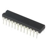
ICGOO电子元器件商城为您提供AD420ANZ-32由Analog设计生产,在icgoo商城现货销售,并且可以通过原厂、代理商等渠道进行代购。 AD420ANZ-32价格参考。AnalogAD420ANZ-32封装/规格:数据采集 - 数模转换器, 16 位 数模转换器 1 24-PDIP。您可以下载AD420ANZ-32参考资料、Datasheet数据手册功能说明书,资料中有AD420ANZ-32 详细功能的应用电路图电压和使用方法及教程。
AD420ANZ-32 是由 Analog Devices Inc. 生产的一款高精度、低功耗的数模转换器(DAC),主要应用于数据采集系统中。该型号具有 16 位分辨率,能够提供非常精细的模拟信号输出控制,适用于需要高精度模拟信号生成的场景。

 应用场景

1. 工业自动化与过程控制:
   AD420ANZ-32 可用于工业自动化系统中的精密控制,例如温度、压力、流量等传感器的信号调理和控制。它能够将数字信号精确转换为模拟信号,驱动执行器或调节阀门,确保生产过程的稳定性和精度。

2. 仪器仪表:
   在精密测量仪器中,AD420ANZ-32 可以用于生成标准的模拟信号,作为校准源或参考信号。其高精度和稳定性使得它在实验室设备、测试仪器等领域具有广泛应用。

3. 通信系统:
   在通信领域,AD420ANZ-32 可用于生成调制信号或控制信号,特别是在无线通信、有线通信及射频(RF)系统中,它能够提供稳定的模拟信号输出,确保通信系统的可靠性和性能。

4. 医疗设备:
   医疗设备如心电图机、超声波设备等需要高精度的模拟信号处理。AD420ANZ-32 可以用于这些设备中,确保信号的准确性和可靠性,从而提高诊断和治疗的效果。

5. 音频设备:
   高保真音频设备对信号的精度要求极高,AD420ANZ-32 可以用于音频信号的数字化处理和还原,确保音质的纯净和真实感。

6. 汽车电子:
   在汽车电子系统中,AD420ANZ-32 可用于发动机控制单元(ECU)、车载信息娱乐系统等,提供精确的模拟信号控制,提升车辆的安全性和舒适性。

7. 航空航天:
   航空航天领域的控制系统对可靠性和精度有极高的要求,AD420ANZ-32 可用于飞行控制、导航系统等关键部位,确保飞行安全和任务成功。

总之,AD420ANZ-32 凭借其高精度、低功耗和稳定性,在多个行业和应用领域中发挥着重要作用,尤其适合那些对模拟信号精度要求极高的应用场景。
| 参数 | 数值 |
| 产品目录 | 集成电路 (IC)半导体 |
| 描述 | IC DAC SRL 16BIT 24-DIP数模转换器- DAC IC 16-BIT |
| 产品分类 | |
| 品牌 | Analog Devices Inc |
| 产品手册 | |
| 产品图片 |
|
| rohs | 符合RoHS无铅 / 符合限制有害物质指令(RoHS)规范要求 |
| 产品系列 | 数据转换器IC,数模转换器- DAC,Analog Devices AD420ANZ-32- |
| 数据手册 | |
| 产品型号 | AD420ANZ-32 |
| 产品培训模块 | http://www.digikey.cn/PTM/IndividualPTM.page?site=cn&lang=zhs&ptm=19145http://www.digikey.cn/PTM/IndividualPTM.page?site=cn&lang=zhs&ptm=18614http://www.digikey.cn/PTM/IndividualPTM.page?site=cn&lang=zhs&ptm=26125http://www.digikey.cn/PTM/IndividualPTM.page?site=cn&lang=zhs&ptm=26140http://www.digikey.cn/PTM/IndividualPTM.page?site=cn&lang=zhs&ptm=26150http://www.digikey.cn/PTM/IndividualPTM.page?site=cn&lang=zhs&ptm=26147 |
| 产品目录页面 | |
| 产品种类 | 数模转换器- DAC |
| 位数 | 16 |
| 供应商器件封装 | 24-PDIP |
| 其它名称 | AD420ANZ32 |
| 分辨率 | 16 bit |
| 包装 | 管件 |
| 商标 | Analog Devices |
| 安装类型 | 通孔 |
| 安装风格 | Through Hole |
| 封装 | Tube |
| 封装/外壳 | 24-DIP(0.300",7.62mm) |
| 封装/箱体 | PDIP-24 |
| 工作温度 | -40°C ~ 85°C |
| 工厂包装数量 | 15 |
| 建立时间 | 2.5µs |
| 接口类型 | SPI |
| 数据接口 | 串行 |
| 最大功率耗散 | 176 mW |
| 最大工作温度 | + 85 C |
| 最小工作温度 | - 40 C |
| 标准包装 | 15 |
| 电压参考 | Internal, External |
| 电压源 | 单电源 |
| 电源电压-最大 | 32 V |
| 电源电压-最小 | 12 V |
| 积分非线性 | +/- 0.012 % FSR |
| 稳定时间 | 2.5 ms |
| 系列 | AD420 |
| 结构 | Delta-Sigma |
| 转换器数 | 1 |
| 转换器数量 | 1 |
| 输出数和类型 | 2 电流,双极 |
| 输出类型 | Current, Voltage |
| 采样比 | 400 SPs |
| 采样率(每秒) | 400 |


- 商务部:美国ITC正式对集成电路等产品启动337调查
- 曝三星4nm工艺存在良率问题 高通将骁龙8 Gen1或转产台积电
- 太阳诱电将投资9.5亿元在常州建新厂生产MLCC 预计2023年完工
- 英特尔发布欧洲新工厂建设计划 深化IDM 2.0 战略
- 台积电先进制程称霸业界 有大客户加持明年业绩稳了
- 达到5530亿美元!SIA预计今年全球半导体销售额将创下新高
- 英特尔拟将自动驾驶子公司Mobileye上市 估值或超500亿美元
- 三星加码芯片和SET,合并消费电子和移动部门,撤换高东真等 CEO
- 三星电子宣布重大人事变动 还合并消费电子和移动部门
- 海关总署:前11个月进口集成电路产品价值2.52万亿元 增长14.8%


PDF Datasheet 数据手册内容提取
Serial Input 16-Bit 4 mA–20 mA, 0 mA–20 mA DAC Data Sheet AD420 FEATURES FUNCTIONAL BLOCK DIAGRAM 4 mA–20 mA, 0 mA–20 mA or 0 mA–24 mA VCC current output VLL REFERENCE 16-bit resolution and monotonicity 4kΩ 40Ω ±0.012% max integral nonlinearity REF OUT AD420 BOOST ±0.05% max offset (trimmable) REF IN ±0.15% max total output error (trimmable) DATA OUT CLOCK Flexible serial digital interface (3.3 MBPS) CLEAR DATA I/P IOUT On-Chip loop fault detection CLLAOTCCHK REGISTER 16-BIT SWITCHED VOUT DAC CURRENT 1.25kΩ On-chip 5 V reference (25 ppm/°C max) DATA IN SOURCES Asynchronous CLEAR function SERLAENCGT E1 FILTAENRDING FDAEUTLETCT Maximum power supply range of 32 V RANGE SELECT 2 Output loop compliance of 0 V to V − 2.75 V 24-Lead SOIC and PDIP packages CC OTFRFSIMET CAP 1 CAP 2 GND 00494-001 Figure 1. GENERAL DESCRIPTION The AD420 is a complete digital to current loop output user desires temperature stability exceeding 25 ppm/°C, an converter, designed to meet the needs of the industrial control external precision reference such as the AD586 can be used as market. It provides a high precision, fully integrated, low cost the reference. The AD420 is available in a 24-lead SOIC and single-chip solution for generating current loop signals in a PDIP over the industrial temperature range of −40°C to +85°C. compact 24-lead SOIC or PDIP package. PRODUCT HIGHLIGHTS The output current range can be programmed to 4 mA to 1. The AD420 is a single chip solution for generating 4 mA to 20 mA, 0 mA to 20 mA or to an overrange function of 0 mA to 20 mA or 0 mA to 20 mA signals at the controller end of 24 mA. The AD420 can alternatively provide a voltage output the current loop. from a separate pin that can be configured to provide 0 V to 5 V, 2. The AD420 is specified with a power supply range from 0 V to 10 V, ±5 V, or ±10 V with the addition of a single external 12 V to 32 V. Output loop compliance is 0 V to V − 2.75 V. buffer amplifier. CC 3. The flexible serial input can be used in 3-wire mode The 3.3 M Baud serial input logic design minimizes the cost of with SPI® or MICROWIRE® microcontrollers, or in galvanic isolation and allows for simple connection to commonly asynchronous mode, which minimizes the number of used microprocessors. It can be used in 3-wire or asynchronous control signals required. mode and a serial-out pin is provided to allow daisy chaining of multiple DACs on the current loop side of the isolation barrier. 4. The serial data out pin can be used to daisy chain any number of AD420s together in 3-wire mode. The AD420 uses sigma-delta (Σ-Δ) DAC technology to achieve 16-bit monotonicity at very low cost. Full-scale settling to 0.1% 5. At power-up, the AD420 initializes its output to the low occurs within 3 ms. The only external components that are end of the selected range. required (in addition to normal transient protection circuitry) 6. The AD420 has an asynchronous CLEAR pin, which sends are two low cost capacitors which are used in the DAC out- the output to the low end of the selected range (0 mA, 4 mA, put filter. or 0 V). If the AD420 is used at extreme temperatures and supply 7. The AD420 BOOST pin accommodates an external voltages, an external output transistor can be used to minimize transistor to off-load power dissipation from the chip. power dissipation on the chip via the BOOST pin. The FAULT 8. The offset of ±0.05% and total output error of ±0.15% can DETECT pin signals when an open circuit occurs in the loop. be trimmed if desired, using two external potentiometers. The on-chip voltage reference can be used to supply a precision +5 V to external components in addition to the AD420 or, if the Rev. I Document Feedback Information furnished by Analog Devices is believed to be accurate and reliable. However, no responsibility is assumed by Analog Devices for its use, nor for any infringements of patents or other One Technology Way, P.O. Box 9106, Norwood, MA 02062-9106, U.S.A. rights of third parties that may result from its use. Specifications subject to change without notice. No license is granted by implication or otherwise under any patent or patent rights of Analog Devices. Tel: 781.329.4700 ©2015 Analog Devices, Inc. All rights reserved. Trademarks and registered trademarks are the property of their respective owners. Technical Support www.analog.com
AD420 Data Sheet TABLE OF CONTENTS Features .............................................................................................. 1 Driving Inductive Loads ............................................................ 10 Functional Block Diagram .............................................................. 1 Voltage-Mode Output ................................................................ 10 General Description ......................................................................... 1 Optional Span and Zero Trim .................................................. 10 Product Highlights ........................................................................... 1 Three-Wire Interface ................................................................. 11 Revision History ............................................................................... 2 Using Multiple DACS with Fault Detect ................................. 11 Specifications ..................................................................................... 3 Asynchronous Interface Using Optocouplers ........................ 11 Absolute Maximum Ratings ............................................................ 5 Microprocessor Interface............................................................... 12 ESD Caution .................................................................................. 5 AD420-To-MC68HC11 (SPI Bus) Interface ........................... 12 Pin Configuration and Function Descriptions ............................. 6 AD420 to Microwire Interface ................................................. 12 Timing Requirements ...................................................................... 7 External Boost Function............................................................ 13 Three-Wire Interface ................................................................... 7 AD420 Protection ........................................................................... 14 Three-Wire Interface Fast Edges on Digital Input ................... 7 Transient Voltage Protection .................................................... 14 Asynchronous Interface ............................................................... 7 Board Layout And Grounding ................................................. 14 Terminology ...................................................................................... 8 Power Supplies and Decoupling ............................................... 14 Theory of Operation ........................................................................ 9 Outline Dimensions ....................................................................... 15 Applications Information .............................................................. 10 Ordering Guide .......................................................................... 15 Current Output ........................................................................... 10 REVISION HISTORY 3/15—Rev. H to Rev. I Changes to Three-Wire Interface Fast Edges on Digital Input Section ................................................................................................ 7 1/11—Rev. G to Rev. H Changes to Figure 13 ...................................................................... 13 Changes to Ordering Guide .......................................................... 15 11/09—Rev. F to Rev. G Updated Format .................................................................. Universal Changes to Table 2 ............................................................................ 5 Updated Outline Dimensions ....................................................... 15 Changes to Ordering Guide .......................................................... 15 9/99—Rev. E to Rev. F Rev. I | Page 2 of 16
Data Sheet AD420 SPECIFICATIONS T = T − T , V = +24 V, unless otherwise noted. A MIN MAX CC Table 1. AD420-32 Version Parameter Min Typ Max Units Comments RESOLUTION 16 Bits I CHARACTERISTICS R = 500 Ω OUT L Operating Current Ranges 4 20 mA 0 20 mA 0 24 mA Current Loop Voltage Compliance 0 V − 2.75 V V CC Settling Time (to 0.1% of FS)1 2.5 3 ms Output Impedance (Current Mode) 25 MΩ Accuracy2 Monotonicity 16 Bits Integral Nonlinearity ±0.002 ±0.012 % Offset (0 mA or 4 mA) (T = +25°C) ±0.05 % A Offset Drift 20 50 ppm/° C Total Output Error (20 mA or 24 mA) (T = +25°C) ±0.15 % A Total Output Error Drift 20 50 ppm/° C PSRR3 5 10 µA/V V CHARACTERISTICS OUT FS Output Voltage Range (Pin 17) 0 5 V VOLTAGE REFERENCE REF OUT Output Voltage (T = +25° C) 4.995 5.0 5.005 V A Drift ±25 ppm/° C Externally Available Current 5 mA Short Circuit Current 7 mA REF IN Resistance 30 kΩ V LL Output Voltage 4.5 V Externally Available Current 5 mA Short Circuit Current 20 mA DIGITAL INPUTS V (Logic 1) 2.4 V IH V (Logic 0) 0.8 V IL I (V = 5.0 V) ±10 µA IH IN I (V = 0 V) ±10 µA IL IN Data Input Rate (3-Wire Mode) No Minimum 3.3 MBPS Data Input Rate (Asynchronous Mode) No Minimum 150 kBPS DIGITAL OUTPUTS FAULT DEFECT V (10 kΩ Pull-Up Resistor to V ) 3.6 4.5 V OH LL V (10 kΩ Pull-Up Resistor to V ) 0.2 0.4 V OL LL V @ 2.5 mA 0.6 V OL DATA OUT V (I = −0.8 mA) 3.6 4.3 V OH OH V (I = 1.6 mA) 0.3 0.4 V OL OL Rev. I | Page 3 of 16
AD420 Data Sheet AD420-32 Version Parameter Min Typ Max Units Comments POWER SUPPLY Operating Range V 12 32 V CC Quiescent Current 4.2 5.5 mA Quiescent Current (External V ) 3 mA LL TEMPERATURE RANGE Specified Performance −40 +85 °C 1 External capacitor selection must be as described in Figure 6. 2 Total Output Error includes Offset and Gain Error. Total Output Error and Offset Error are with respect to the Full-Scale Output and are measured with an ideal +5 V reference. If the internal reference is used, the reference errors must be added to the Offset and Total Output Errors. 3 PSRR is measured by varying VCC from 12 V to its maximum 32 V. Rev. I | Page 4 of 16
Data Sheet AD420 ABSOLUTE MAXIMUM RATINGS Table 3. Truth Table Table 2. Inputs Parameter Rating Range Range V to GND 32 V CC CLEAR Select 2 Select 1 Operation I to GND V OUT CC 0 X X Normal operation Digital Inputs to GND −0.5 V to +7 V 1 X X Output at bottom of Digital Output to GND −0.5 V to V + 0.3 V LL span V and REF OUT: Outputs Safe for LL X 0 0 0 V–5 V range Indefinite Short to Ground X 0 1 4 mA–20 mA range Storage Temperature −65°C to +150°C X 1 0 0 mA–20 mA range Lead Temperature (Soldering, 10 sec) +300°C X 1 1 0 mA–24 mA range Lead Temperature, Soldering Reflow +260°C Thermal Impedance: SOIC (R) Package θJA = 75°C/W ESD CAUTION PDIP (N) Package θ = 50°C/W JA Stresses at or above those listed under Absolute Maximum Ratings may cause permanent damage to the product. This is a stress rating only; functional operation of the product at these or any other conditions above those indicated in the operational section of this specification is not implied. Operation beyond the maximum operating conditions for extended periods may affect product reliability. Rev. I | Page 5 of 16
AD420 Data Sheet PIN CONFIGURATION AND FUNCTION DESCRIPTIONS NC 1 24 NC VLL 2 23 VCC FAULT DETECT 3 22 NC RANGE SELECT 2 4 21 CAP 2 RANGE SELECT 1 5 AD420 20 CAP 1 CLEAR 6 TOP VIEW 19 BOOST (Not to Scale) LATCH 7 18 IOUT CLOCK 8 17 VOUT DATA IN 9 16 OFFSET TRIM DATA OUT 10 15 REF IN GND 11 14 REF OUT NC 1N2C = NO CONNEC1T3 NC 00494-002 Figure 2. Pin Configuration Table 4. Pin Function Descriptions Pin No. Mnemonic Function 1, 12, NC No Connection. No internal connections inside device. 13, 24 2 V Auxiliary buffered +4.5 V digital logic voltage. This pin is the internal supply voltage for the digital LL circuitry and can be used as a termination for pull-up resistors. An external +5 V power supply can be connected to V . It will override this buffered voltage, thus reducing the internal power dissipation. The LL V pin should be decoupled to GND with a 0.1 µF capacitor. See the Power Supplies and Decoupling LL section. 3 FAULT DETECT FAULT DETECT, connected to a pull-up resistor, is asserted low when the output current does not match the DAC’s programmed value, for example, in case the current loop is broken. 4 RANGE SELECT 2 Selects the converter’s output operating range. One output voltage range and three 5 RANGE SELECT 1 output current ranges are available. 6 CLEAR Valid V unconditionally forces the output to go to the minimum of its programmed range. After CLEAR IH is removed the DAC output will remain at this value. The data in the input register is unaffected. 7 LATCH In the 3-wire interface mode a rising edge parallel loads the serial input register data into the DAC. To use the asynchronous mode connect LATCH through a current limiting resistor to V . CC 8 CLOCK Data Clock Input. The clock period is equal to the input data bit rate in the 3-wire interface mode and is 16 times the bit rate in asynchronous mode. 9 DATA IN Serial Data Input. 10 DATA OUT Serial Data Output. In the 3-wire interface mode, this output can be used for daisy-chaining multiple AD420s. In the asynchronous mode a positive pulse will indicate a framing error after the stop-bit is received. 11 GND Ground (Common). 14 REF OUT +5 V Reference Output. 15 REF IN Reference Input. 16 OFFSET TRIM Offset Adjust. 17 V Voltage Output. OUT 18 I Current Output. OUT 19 BOOST Connect to an external transistor to reduce the power dissipated in the AD420 output transistor, if desired. 20 CAP 1 These pins are used for internal filtering. Connect capacitors between each of these 21 CAP 2 pins and V . Refer to the description of current output operation. CC 22 NC No Connection. Do not connect anything to this pin. 23 V Power Supply Input. The V pin should always be decoupled to GND with a 0.1 µF capacitor. See the CC CC Power Supplies and Decoupling section. Rev. I | Page 6 of 16
Data Sheet AD420 TIMING REQUIREMENTS T = −40°C to +85°C, V = +12 V to +32 V. A CC CLOCK THREE-WIRE INTERFACE DATA IN 0 1 0 0 1 CLOCK WORD “N” WORD “N + 1” STARTBIT BIT15 BIT14 BIT13O BIT1 BIT0 STOPBIT NEXTSTARTBIT T DATA IN 1 0 1 1 0 0 1 0 0 1 1 1 0 0 1 1 1 0 0 1 (INTERNALLY GENERATED LATCH) SB)B15B14B13B12B11 B10B9 B8B7B6B5B4B3 B2B1B0 SB)B15B14 B13B12 (M (L EXPANDED TIME VIEW BELOW LATCH CLOCK COUNTER STARTS HERE CONFIRMSTARTBIT SAMPLE BIT 15 WORD “N – 1” WORD “N” DATA OUT 1 0 1 1 CLOCK 5 4 32 0 1 2 8 16 24 tCK B1 B1 B1B1 tCL DATA IN START BIT DATA BIT 15 BIT 14 CLOCK tCH tDS tDH EXPtAACNKDED TIME VIEW BELOW DATA IN tACL CLOCK tDW tACH tLD tADS tADH LATCH tLLtSD tLH DATA IN tADW 00494-004 DATA OUT 00494-003 Figure 4. Timing Diagram for Asynchronous Interface Figure 3. Timing Diagram for 3-Wire Interface Table 6. Timing Specifications for Asynchronous Interface Parameter Label Limit Units Table 5. Timing Specification for 3-Wire Interface Asynchronous Clock Period t 400 ns min ACK Parameter Label Limit Units Asynchronous Clock Low Time t 50 ns min ACL Data Clock Period t 300 ns min CK Asynchronous Clock High Time t 150 ns min ACH Data Clock Low Time t 80 ns min CL Data Stable Width (Critical Clock Edge) t 300 ns min ADW Data Clock High Time t 80 ns min CH Data Setup Time (Critical Clock Edge) t 60 ns min ADS Data Stable Width t 125 ns min DW Data Hold Time (Critical Clock Edge) t 20 ns min ADH Data Setup Time t 40 ns min DS Clear Pulse Width t 50 ns min CLR Data Hold Time t 5 ns min DH ASYNCHRONOUS INTERFACE Latch Delay Time t 80 ns min LD Latch Low Time tLL 80 ns min Note that in the timing diagram for asynchronous mode oper- Latch High Time tLH 80 ns min ation each data word is framed by a START (0) bit and a STOP Serial Output Delay Time tSD 225 ns max (1) bit. The data timing is with respect to the rising edge of the Clear Pulse Width tCLR 50 ns min CLOCK at the center of each bit cell. Bit cells are 16 clocks THREE-WIRE INTERFACE FAST EDGES ON DIGITAL long, and the first cell (the START bit) begins at the first clock INPUT following the leading (falling) edge of the START bit. Thus, the MSB (D15) is sampled 24 clock cycles after the beginning of With a fast rising edge (<100 ns) on one of the serial inputs the START bit, D14 is sampled at clock number 40, and so on. (CLOCK, DATA IN, LATCH) while another input is logic high, During any dead time before writing the next word the DATA the part may be triggered into a test mode and the contents of IN pin must remain at Logic 1. the data register may become corrupted, which may result in The DAC output updates when the STOP bit is received. In the output being loaded with an incorrect value. If fast edges are the case of a framing error (the STOP bit sampled as a 0) the expected on the digital input lines, it is recommended that the AD420 will output a pulse at the DATA OUT pin one clock latch line remain at Logic 0 during serial loading of the DAC. period wide during the clock period subsequent to sampling Similarly, the clock line should remain low during updates of the STOP bit. The DAC output will not update if a framing the DAC via the latch pin. Alternatively, the addition of small error is detected. value capacitors on the digital lines will slow down the edge. Rev. I | Page 7 of 16
AD420 Data Sheet TERMINOLOGY Gain Error Resolution Gain error is a measure of the output error between an ideal For 16-bit resolution, 1 LSB = 0.0015% of the FSR. In the DAC and the actual device output with all 1s loaded after offset 4 mA–20 mA range 1 LSB = 244 nA. error has been adjusted out. Integral Nonlinearity Offset Error Analog Devices defines integral nonlinearity as the maximum Offset error is the deviation of the output current from its ideal deviation of the actual, adjusted DAC output from the ideal value expressed as a percentage of the fullscale output with all analog output (a straight line drawn from 0 to FS – 1 LSB) for 0s loaded in the DAC. any bit combination. This is also referred to as relative accuracy. Drift Differential Nonlinearity Drift is the change in a parameter (such as gain and offset) over Differential nonlinearity is the measure of the change in the a specified temperature range. The drift temperature coefficient, analog output, normalized to full scale, associated with an LSB specified in ppm/°C, is calculated by measuring the parameter change in the digital input code. Monotonic behavior requires at T , 25°C, and T and dividing the change in the that the differential linearity error be greater than –1 LSB over MIN MAX parameter by the corresponding temperature change. the temperature range of interest. Current Loop Voltage Compliance Monotonicity The voltage compliance is the maximum voltage at the I pin for A DAC is monotonic if the output either increases or remains OUT which the output current will be equal to the programmed value. constant for increasing digital inputs with the result that the output will always be a single-valued function of the input. Rev. I | Page 8 of 16
Data Sheet AD420 THEORY OF OPERATION The AD420 uses a sigma-delta (Σ-Δ) architecture to carry out approximately one volt remaining of drive capability (when the digital-to-analog conversion. This architecture is particularly the gate of the output PMOS transistor nearly reaches ground). well suited for the relatively low bandwidth requirements of the Thus the FAULT DETECT output activates slightly before the industrial control environment because of its inherent compliance limit is reached. Since the comparison is made monotonicity at high resolution. within the feedback loop of the output amplifier, the output accuracy is maintained by its open-loop gain, and no output In the AD420 a second order modulator is used to keep com- error occurs before the fault detect output becomes active. plexity and die size to a minimum. The single bit stream from the modulator controls a switched current source that is then The 3-wire digital interface, comprising DATA IN, CLOCK, filtered by two, continuous time resistor-capacitor sections. and LATCH, interfaces to all commonly used serial micropro- The capacitors are the only external components that have to be cessors without the addition of any external glue logic. Data is added for standard current-out operation. The filtered current loaded into an input register under control of CLOCK and is is amplified and mirrored to the supply rail so that the application loaded to the DAC when LATCH is strobed. If a user wants to simply sees a 4 mA–20 mA, 0 mA–20 mA, or 0 mA–24 mA minimize the number of galvanic isolators in an intrinsically current source output with respect to ground. The AD420 safe application, the AD420 can be configured to run in is manufactured on a BiCMOS process that is well suited to asynchronous mode. This mode is selected by connecting the implementing low voltage digital logic with high performance LATCH pin to V through a current limiting resistor. The data CC and high voltage analog circuitry. must then be combined with a start and stop bit to frame the information and trigger the internal LATCH signal. The AD420 can also provide a voltage output instead of a current loop output if desired. The addition of a single external amplifier VCC 23 allows the user to obtain 0 V–5 V, 0 V–10 V, ±5 V, or ±10 V. VLL 2 REFERENCE The AD420 has a loop fault detection circuit that warns if the 4kΩ 40Ω voltage at IOUT attempts to rise above the compliance range, due REF OUT 14 AD420 19 BOOST to an open-loop circuit or insufficient power supply voltage. The REF IN 15 FAULT DETECT is an active low open drain signal so that one DATA OUT 10 CLOCK can connect several AD420s together to one pull-up resistor for CLEAR 6 18 IOUT global error detection. The pull-up resistor can be tied to the LATCH 7 RDEAGTIAS TI/EPR 16-BIT SWITCHED 17 VOUT CLOCK 8 DAC CURRENT 1.25kΩ V pin, or an external +5 V logic supply. SOURCES LL DATA IN 9 AND 3 DFAEUTELTCT The IOUT current is controlled by a PMOS transistor and an SERLAENCGT E1 5 FILTERING internal amplifier as shown in the functional block diagram. RANGE 4 SELECT 2 The internal circuitry that develops the fault output avoids uansi nacgt ua aclo omuptpaurat teorrr owri tbhe fwoirned tohwe FliAmUitLsT s iDncEeT tEhCisT w oouutlpdu rte quire OTFRF16SIMET CA20P 1 CA2P1 2 G1N1D 00494-005 Figure 5. Functional Block Diagram becomes active. Instead, the signal is generated when the internal amplifier in the output stage of the AD420 has less than Rev. I | Page 9 of 16
AD420 Data Sheet APPLICATIONS INFORMATION CURRENT OUTPUT Table 7. Buffer Amplifier Configuration The AD420 can provide 4 mA–20 mA, 0 mA–20 mA, or 0 mA– R1 R2 R3 VOUT 24 mA output without any active external components. Filter Open Open 0 0 V − 5 V capacitors C1 and C2 can be any type of low cost ceramic Open R R capacitors. To meet the specified full-scale settling time of 3 ms, R Open R ±5 V low dielectric absorption capacitors (NPO) are required. R 2R 2R ±10 V Suitable values are C1 = 0.01 µF and C2 = 0.01 µF. Suitable R = 5 kΩ. 0.1µF VLL VCC 0.1µF OPTIONAL SPAN AND ZERO TRIM C1 C2 For users who would like lower than the specified values of 2 20 21 23 offset and gain error, Figure 8 shows a simple way to trim these RANGE SELECT 1 5 parameters. Care should be taken to select low drift resistors RANGE 4 because they affect the temperature drift performance of SELECT 2 IOUT (4mATO 20mA) CLEAR 6 18 the DAC. AD420 LATCH 7 RLOAD The adjustment algorithm is iterative. The procedure for CLOCK 8 trimming the AD420 in the 4 mA–20 mA mode can be DATA IN 9 accomplished as follows: REF OUT14 15REF IN 11GND 00494-006 1. Offset adjust. Load all zeros. Adjust RZERO for Figure 6. Standard Configuration 4.00000 mA of output current. 2. Gain adjust. Load all ones. Adjust RSPAN for 19.99976 mA DRIVING INDUCTIVE LOADS (FS − 1 LSB) of output current. When driving inductive or poorly defined loads ,connect a 0.01 µF Return to Step I and iterate until convergence is obtained. capacitor between I (Pin 18) and GND (Pin 11). This ensures OUT stability of the AD420 with loads beyond 50 mH. There is no VCC VLL maximum capacitance limit. The capacitive component of the 0.1µF C1 C2 0.1µF load may cause slower settling, though this may be masked by 5kΩ the settling time of the AD420. A programmed change in the RANGE 2 20 21 23 RSPAN2 SELECT 1 5 current may cause a back EMF voltage on the output that may RANGE 4 19 BOOST exceed the compliance of the AD420. To prevent this voltage SELECT 2 from exceeding the supply rails connect protective diodes CLEAR 6 AD420 18IOUT (4mATO 20mA) between IOUT and each of VCC and GND. LATCH 7 RLOAD CLOCK 8 VOLTAGE-MODE OUTPUT DATA IN 9 Since the AD420 is a single supply device, it is necessary to add REF OUT14 15 16 11 an external buffer amplifier to the V pin to obtain a selection OUT 500Ω of bipolar output voltage ranges aVsC Cshown in Figure 7. RSPAN R1Z0EkRΩO GND 00494-008 0.1µF VLL Figure 8. Offset and Gain Adjust 0.1µF C1 C2 Variation of RZERO between REF OUT (5 V) and GND leads 2 20 21 23 RANGE to an offset adjust range from −1.5 mA to 6 mA, (1.5 mA/V SELECT 1 5 RANGE 4 centered at 1 V). SELECT 2 VOUT CLEAR 6 17 The 5 kΩ RSPAN2 resistor is connected in parallel with the AD420 VOUT LATCH 7 R3 internal 40 W sense resistor, which leads to a gain increase of +0.8%. CLOCK 8 R1 R2 DATA IN 9 As RSPAN is changed to 500 Ω, the voltage on REF IN is REF OUT14 15REF IN 11GND 00494-007 ainttpeuntu raetseidst bany cteh.e W cohmenb iandadtieodn t oofg eRtShPeAr wNi tahn dR SthPeA 3N02 k tΩhi sR EF IN Figure 7. results in an adjustment range of −0.8% to +0.8%. Rev. I | Page 10 of 16
Data Sheet AD420 THREE-WIRE INTERFACE ASYNCHRONOUS INTERFACE USING OPTOCOUPLERS Figure 9 shows the AD420 connected in the 3-wire interface mode. The AD420 data input block contains a serial input shift The AD420 connected in asynchronous interface mode with register and a parallel latch. The contents of the shift register optocouplers is shown in Figure 10. Asynchronous operation are controlled by the DATA IN signal and the rising edges of the minimizes the number of control signals required for isolation CLOCK. Upon request of the LATCH pin the DAC and internal of the digital system from the control loop. The resistor connected latch are updated from the shift register parallel outputs. The between the LATCH pin and V is required to activate this CC CLOCK should remain inactive while the DAC is updated. mode. For operation with V below 18 V use a 50 kΩ pull-up CC Refer to the timing requirements for 3-wire interface. resistor; from 18 V to 32 V, use 100 kΩ. Asynchronous mode requires that the clock run at 16 times the FAULT DETECT data bit rate, therefore, to operate at the maximum input data rate ADDA4C210 VCC VLL ADDA4C220 VCC of 150 kBPS, an input clock of 2.4 MHz is required. The actual 10kΩ data rate achieved may be limited by the type of optocouplers FDAEUTLETCT VCC FDAEUTLETCT VCC chosen. The number of control signals can be further reduced LATCH LATCH LATCH by creating the appropriate clock signal on the current loop CLOCK CLOCK CLOCK side of the isolation barrier. If optocouplers with relatively slow DATA IN DATA DATA DATA DATA rise and fall times are used, Schmitt triggers may be required on IN OUT IN OUT the digital inputs to prevent erroneous data being presented to GND IOUT GND IOUT RLOAD RLOAD 00494-009 the DAC. +24V Figure 9. Three-Wire Interface Using Multiple DACs with Joint Fault Detect 23 VCC AD420 USING MULTIPLE DACS WITH FAULT DETECT 100kΩ 7 LATCH The 3-wire interface mode can utilize the serial DATA OUT for +5V 2 VLL easy interface to multiple DACs. To program the two AD420s in Figure 9, 32 data bits are required. The first 16 bits are clocked 8 CLOCK into the input shift register of DAC1. The next 16 bits CLOCK transmitted pass the first 16 bits from the DATA OUT pin of 9 DATA IN DAC1 to the input register of DAC2. The input shift registers of the two DACs operate as a single 32-bit shift register, with the DATA 11 GND lteraaidliinngg 1166 bbiittss sreeprvreinsegn ftoirn gD iAnCfo1r.m Eaatciho nD fAoCr D isA tChe2n a nupd dtahtee d GBAALRVARNIEIRC ISOLATION 00494-010 upon request of the LATCH pin. The daisy-chain can be Figure 10. Asynchronous Interface Using Optocouplers extended to as many DACs as required. Rev. I | Page 11 of 16
AD420 Data Sheet MICROPROCESSOR INTERFACE AD420-TO-MC68HC11 (SPI BUS) INTERFACE The SPI data port is configured to process data in 8-bit bytes. The most significant data byte (MSBY) is retrieved from The AD420 interface to the Motorola serial peripheral interface memory and processed by the SENDAT routine. The SS pin is (SPI) is shown in Figure 11. The MOSI, SCK, and SS pins of the driven low by indexing into the PORTD data register and clear HC11 are respectively connected to the DATA IN, CLOCK, and Bit 5. The MSBY is then sent to the SPI data register where it is LATCH pins of the AD420. The majority of the interfacing automatically transferred to the AD420 internal shift resister. issues are done in the software initialization. A typical routine, The HC11 generates the requisite eight clock pulses with data such as the one shown below, begins by initializing the state of valid on the rising edges. After the MSBY is transmitted, the the various SPI data and control registers. least significant byte (LSBY) is loaded from memory and INIT LDAA #$2F ; SS = 1; SCK = 0; transmitted in a similar fashion. To complete the transfer, the MOSI = 1 LATCH pin is driven high when loading the complete 16-bit STAA PORTD ;SEND TO SPI OUTPUTS word into the AD420. LDAA #$38 ; SS, SCK, MOSI = OUTPUTS MOSI DATA IN 68HC11 SCK CLOCK AD420 STAA DDRD ;ISNEFNOD DATA DIRECTION SS LATCH 00494-011 LDAA #$50 ;DABL INTRPTS, SPI Figure 11. AD420-to-68HC11 (SPI) Interface IS MASTER & ON AD420 TO MICROWIRE INTERFACE STAA SPCR ;CPOL = 0, CPHA = 0, 1MHZ BAUDRATE The flexible serial interface of the AD420 is also compatible NEXTPT LDAA MSBY ;LOAD ACCUM W/UPPER with the National Semiconductor MICROWIRE interface. The 8 BITS MICROWIRE interface is used in microcontrollers such as the BSR SENDAT ;JUMP TO DAC OUTPUT COP400 and COP800 series of processors. A generic interface ROUTINE to use the MICROWIRE interface is shown in Figure 12. The JMP NEXTPT ;INFINITE LOOP G1, SK, and SO pins of the MICROWIRE interface are ;POINT AT ON-CHIP SENDAT LDY #$1000 respectively connected to the LATCH, CLOCK, and DATA IN REGISTERS pins of the AD420. BCLR $08,Y,$20 ;DRIVE SS (LATCH) LOW SO DATA IN STAA SPDR ;SEND MS-BYTE TO SPI MICROWIRE WAIT1 LDAA SPSR D;ACTHAE CRKE GS TA TUS OF SGK1 CLALTOCCHK AD420 00494-012 SPIE Figure 12. AD420-to-MICROWIRE Interface BPL WAIT1 ;POLL FOR END OF X- MISSION LDAA LSBY ;GET LOW 8 BITS FROM MEMORY ;SEND LS-BYTE TO SPI STAA SPDR DATA REG WAIT2 LDAA SPSR ;CHECK STATUS OF SPIE BPL WAIT2; ;POLL FOR END OF X- MISSION BSET $08,Y,$20 ;DRIVE SS HIGH TO LATCH DATA RTS Rev. I | Page 12 of 16
Data Sheet AD420 EXTERNAL BOOST FUNCTION transistor. The plot in Figure 14 shows the safe operating region for both package types. The boost transistor can also be used to The external boost transistor reduces the power dissipated in reduce the amount of temperature induced drift in the part. the AD420 by reducing the current flowing in the on-chip This will minimize the temperature induced drift of the on-chip output transistor (dividing it by the current gain of the external voltage reference, which improves drift and linearity. circuit). A discrete NPN transistor with a breakdown voltage, BVCEO, greater than 32 V can be used as shown in Figure 13. VCC WANH EENX TUESRINNGAL S BOOICO PSATC TKRAAGNESDIS DTEOVRI CISES, MJD31C REQUIRED FOR OPERATION IN THIS AREA. OR 2N3053 BOOST 19 32V AD420 28V IOUT 18 25V 0.022µF 1kΩ RLOAD 00494-013 20V AD420 OR AD420-32 Figure 13. External Boost Configuration 12V The external boost capability has been developed for those users who may wish to use the AD420, in the SOIC package, at the extremes of the supply voltage, load current, and 4V ttehmerpmearal truerseis rtaanncgee). Twhilel oPpDeIrPa tpe ascakfealgye o(vbeerc athues ee notfi irtes slopweceirf ied –60 –40 –20 TE0MPER2A0TURE 4(°0C) 60 80 100 00494-014 voltage, temperature, and load current ranges without the boost Figure 14. Safe Operating Region Rev. I | Page 13 of 16
AD420 Data Sheet AD420 PROTECTION BOARD LAYOUT AND GROUNDING The AD420 ground pin, designated GND, is the high quality TRANSIENT VOLTAGE PROTECTION ground reference point for the device. Any external loads on the The AD420 contains ESD protection diodes, which prevent REF OUT and V pins of the AD420 should be returned to OUT damage from normal handling. The industrial control envir- this reference point. Analog and digital ground currents should onment can, however, subject I/O circuits to much higher not share a common path. Each signal should have an appropriate transients. To protect the AD420 from excessively high voltage analog or digital signal return routed close to it. Using this transients, such as those specified in IEC 801, external power approach, signal loops enclose a small area, minimizing the diodes and a surge current limiting resistor may be required, as inductive coupling of noise. Wide PC tracks, large gauge wire, shown in Figure 15. The constraint on the resistor is that during and ground planes are highly recommended to provide low normal operation the output voltage level at IOUT must remain impedance signal paths. within its voltage compliance limit POWER SUPPLIES AND DECOUPLING (I × (Rp + R ) ≤ V − 2.75 V) OUT LOAD CC The AD420 supply pins, V (Pin 23) and V (Pin 2), should be CC LL and the two protection diodes and resistor must have decoupled to GND with 0.1 µF capacitors to eliminate high appropriate power ratings. frequency noise that may otherwise get coupled into the analog VCC system. High frequency ceramic capacitors are recommended. The decoupling capacitors should be located in close proximity to the pins and the ground line to have maximum effect. Further VCC reductions in noise, and improvements in performance, may be AD420 IOUT RP achieved by using a larger value capacitor on the VLL pin. GND RLOAD 00494-015 Figure 15. Output Transient Voltage Protection Rev. I | Page 14 of 16
Data Sheet AD420 OUTLINE DIMENSIONS 1.280 (32.51) 1.250 (31.75) 1.230 (31.24) 24 13 0.280 (7.11) 0.250 (6.35) 1 12 0.240 (6.10) 0.325 (8.26) 0.310 (7.87) 0.100 (2.54) 0.300 (7.62) BSC 0.060 (1.52) 0.195 (4.95) 0.210 (5.33) MAX 0.130 (3.30) MAX 0.115 (2.92) 0.015 0.150 (3.81) (0.38) 0.015 (0.38) 0.130 (3.30) MIN GAUGE 0.115 (2.92) SPLEAATNIENG PLANE 00..001140 ((00..3265)) 0.022 (0.56) 0.008 (0.20) 0.005 (0.13) 0.430 (10.92) 0.018 (0.46) MIN MAX 0.014 (0.36) 0.070 (1.78) 0.060 (1.52) 0.045 (1.14) COMPLIANTTO JEDEC STANDARDS MS-001 CONTROLLING DIMENSIONSARE IN INCHES; MILLIMETER DIMENSIONS (RCINOEFRPENARREEREN NLCTEEHA EODSNSEL MSY)AAAYNR BDEE AR CROOEU NNNFODIGETUDAR-POEPFDRFOA INSPC RWHIAH ETOEQL UFEIO VORAR LU EHSNAETL ISFN FLDOEEARSDIGS.N. 071006-A Figure 16. 24-Lead Plastic Dual In-Line Package [PDIP] Narrow Body (N-24-1) Dimensions shown in inches and (millimeters) 15.60(0.6142) 15.20(0.5984) 24 13 7.60(0.2992) 7.40(0.2913) 1 12 10.65(0.4193) 10.00(0.3937) 0.75(0.0295) 45° 2.65(0.1043) 0.25(0.0098) 0.30(0.0118) 2.35(0.0925) 8° 0.10(0.0039) 0° COPLANARITY 0.10 1.27B(0S.C0500) 00..5311((00..00210212)) SPLEAATNIENG 00..3230((00..00103709)) 10..2470((00..00510507)) COMPLIANTTOJEDECSTANDARDSMS-013-AD C(RINOEFNPEATRRREOENNLCLTEIHNEOGSNDELISYM)AEANNRDSEIAORRNOESUNANORDETEDAIN-POMPFRIFLOLMPIMIRLELIATIMTEEERTFSEO;RIRNECUQHSUEDIVIINMAELDENENSSTIIOGSNNFS.OR 12-09-2010-A Figure 17. 24-Lead Standard Small Outline [SOIC_W] Wide Body (RW-24) Dimensions shown in millimeters and (inches) ORDERING GUIDE Model1 Temperature Range Max Operating Voltage Package Description Package Option AD420AN-32 −40°C to +85°C 32 V 24-Lead PDIP N-24-1 AD420ANZ-32 −40°C to +85°C 32 V 24-Lead PDIP N-24-1 AD420AR-32 −40°C to +85°C 32 V 24-Lead SOIC_W RW-24 AD420AR-32-REEL −40°C to +85°C 32 V 24-Lead SOIC_W RW-24 AD420ARZ-32 −40°C to +85°C 32 V 24-Lead SOIC_W RW-24 AD420ARZ-32-REEL −40°C to +85°C 32 V 24-Lead SOIC_W RW-24 1 Z = RoHS Compliant Part. Rev. I | Page 15 of 16
AD420 Data Sheet NOTES ©2015 Analog Devices, Inc. All rights reserved. Trademarks and registered trademarks are the property of their respective owners. D00494-0-3/15(I) Rev. I | Page 16 of 16
Mouser Electronics Authorized Distributor Click to View Pricing, Inventory, Delivery & Lifecycle Information: A nalog Devices Inc.: AD420AN-32 AD420AR-32 AD420AR-32-REEL AD420ARZ-32-REEL AD420ANZ-32 AD420ARZ-32