ICGOO在线商城 > 集成电路(IC) > 数据采集 - 数模转换器 > AD5327BRUZ
 Datasheet下载
- 型号: AD5327BRUZ
- 制造商: Analog
- 库位|库存: xxxx|xxxx
- 要求:
| 数量阶梯 | 香港交货 | 国内含税 |
| +xxxx | $xxxx | ¥xxxx |
查看当月历史价格
查看今年历史价格
AD5327BRUZ产品简介:
ICGOO电子元器件商城为您提供AD5327BRUZ由Analog设计生产,在icgoo商城现货销售,并且可以通过原厂、代理商等渠道进行代购。 AD5327BRUZ价格参考¥131.13-¥161.39。AnalogAD5327BRUZ封装/规格:数据采集 - 数模转换器, 12 位 数模转换器 4 16-TSSOP。您可以下载AD5327BRUZ参考资料、Datasheet数据手册功能说明书,资料中有AD5327BRUZ 详细功能的应用电路图电压和使用方法及教程。
AD5327BRUZ 是由 Analog Devices Inc. 生产的一款数模转换器(DAC),具有12位分辨率,双通道输出,并内置电压基准。该器件广泛应用于需要高精度模拟信号生成的场合。其主要应用场景包括:

1. 工业自动化与控制系统:用于PLC(可编程逻辑控制器)或工业仪表中,将数字控制信号转换为模拟电压,以驱动执行机构如阀门、电机等。

2. 测试与测量设备:在自动测试设备(ATE)、信号发生器和校准仪器中,提供高精度、稳定的模拟输出信号,用于测试被测设备的性能。

3. 通信系统:用于基站或通信模块中的偏置电压调节、功率控制等环节,确保射频或光模块工作在最佳状态。

4. 医疗设备:如监护仪、诊断设备中的传感器激励或信号调理电路,要求高稳定性和低噪声的模拟输出。

5. 汽车电子:用于车载控制系统中,例如发动机管理系统的传感器校准或执行器控制。

AD5327BRUZ 采用TSSOP封装,支持I²C接口通信,适合嵌入到各种嵌入式系统中,具备良好的集成性和可靠性,适用于对精度和稳定性有较高要求的中高端应用场合。
| 参数 | 数值 |
| 产品目录 | 集成电路 (IC)半导体 |
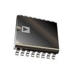
| 描述 | IC DAC 12BIT QUAD 2.5V 16-TSSOP数模转换器- DAC IC 12-BIT QUAD |
| 产品分类 | |
| 品牌 | Analog Devices |
| 产品手册 | |
| 产品图片 |
|
| rohs | 符合RoHS无铅 / 符合限制有害物质指令(RoHS)规范要求 |
| 产品系列 | 数据转换器IC,数模转换器- DAC,Analog Devices AD5327BRUZ- |
| 数据手册 | |
| 产品型号 | AD5327BRUZ |
| 产品培训模块 | http://www.digikey.cn/PTM/IndividualPTM.page?site=cn&lang=zhs&ptm=19145http://www.digikey.cn/PTM/IndividualPTM.page?site=cn&lang=zhs&ptm=18614http://www.digikey.cn/PTM/IndividualPTM.page?site=cn&lang=zhs&ptm=26125http://www.digikey.cn/PTM/IndividualPTM.page?site=cn&lang=zhs&ptm=26140http://www.digikey.cn/PTM/IndividualPTM.page?site=cn&lang=zhs&ptm=26150http://www.digikey.cn/PTM/IndividualPTM.page?site=cn&lang=zhs&ptm=26147 |
| 产品目录页面 | |
| 产品种类 | 数模转换器- DAC |
| 位数 | 12 |
| 供应商器件封装 | 16-TSSOP |
| 分辨率 | 12 bit |
| 包装 | 管件 |
| 商标 | Analog Devices |
| 安装类型 | 表面贴装 |
| 安装风格 | SMD/SMT |
| 封装 | Tube |
| 封装/外壳 | 16-TSSOP(0.173",4.40mm 宽) |
| 封装/箱体 | TSSOP-16 |
| 工作温度 | -40°C ~ 105°C |
| 工厂包装数量 | 96 |
| 建立时间 | 8µs |
| 接口类型 | SPI |
| 数据接口 | DSP,MICROWIRE™,QSPI™,串行,SPI™ |
| 最大功率耗散 | 4.5 mW |
| 最大工作温度 | + 105 C |
| 最小工作温度 | - 40 C |
| 标准包装 | 1 |
| 电压参考 | External |
| 电压源 | 单电源 |
| 电源电压-最大 | 5.5 V |
| 电源电压-最小 | 2.5 V |
| 积分非线性 | +/- 10 LSB |
| 稳定时间 | 8 us |
| 系列 | AD5327 |
| 结构 | Resistor String |
| 转换器数 | 4 |
| 转换器数量 | 4 |
| 输出数和类型 | 4 电压,单极4 电压,双极 |
| 输出类型 | Voltage |
| 采样比 | 125 kSPs |
| 采样率(每秒) | 125k |


- 商务部:美国ITC正式对集成电路等产品启动337调查
- 曝三星4nm工艺存在良率问题 高通将骁龙8 Gen1或转产台积电
- 太阳诱电将投资9.5亿元在常州建新厂生产MLCC 预计2023年完工
- 英特尔发布欧洲新工厂建设计划 深化IDM 2.0 战略
- 台积电先进制程称霸业界 有大客户加持明年业绩稳了
- 达到5530亿美元!SIA预计今年全球半导体销售额将创下新高
- 英特尔拟将自动驾驶子公司Mobileye上市 估值或超500亿美元
- 三星加码芯片和SET,合并消费电子和移动部门,撤换高东真等 CEO
- 三星电子宣布重大人事变动 还合并消费电子和移动部门
- 海关总署:前11个月进口集成电路产品价值2.52万亿元 增长14.8%


PDF Datasheet 数据手册内容提取
2.5 V to 5.5 V, 400 μA, Quad Voltage Output, 8-/10-/12-Bit DACs in 16-Lead TSSOP Data Sheet AD5307/AD5317/AD5327 FEATURES GENERAL DESCRIPTION AD5307: 4 buffered 8-bit DACs in 16-lead TSSOP The AD5307/AD5317/AD53271 are quad 8-,10-,12-bit buffered A version: ±1 LSB INL; B version: ±0.625 LSB INL voltage-output DACs in 16-lead TSSOP that operate from single AD5317: 4 buffered 10-bit DACs in 16-lead TSSOP A version: ±4 LSB INL; B version: ±2.5 LSB INL 2.5 V to 5.5 V supplies and consume 400 μA at 3 V. Their on- AD5327: 4 buffered 12-bit DACs in 16-lead TSSOP chip output amplifiers allow the outputs to swing rail-to-rail with A version: ±16 LSB INL; B version: ±10 LSB INL a slew rate of 0.7 V/μs. The AD5307/AD5317/AD5327 utilize Low power operation: 400 μA @ 3 V, 500 μA @ 5 V versatile 3-wire serial interfaces that operate at clock rates up to 2.5 V to 5.5 V power supply 30 MHz; these parts are compatible with standard SPI, QSPI, Guaranteed monotonic by design over all codes MICROWIRE, and DSP interface standards. Power down to 90 nA @ 3 V, 300 nA @ 5 V (LDAC pin) Double-buffered input logic The references for the four DACs are derived from two reference Buffered/unbuffered reference input options pins (one per DAC pair). These reference inputs can be configured Output range: 0 V to V or 0 V to 2 V as buffered or unbuffered inputs. Each part incorporates a power- REF REF Power-on reset to 0 V on reset circuit, ensuring that the DAC outputs power up to 0 V Simultaneous update of outputs (LDAC pin) and remain there until a valid write to the device takes place. Asynchronous clear facility (CLR pin) There is also an asynchronous active low CLR pin that clears all Low power, SPI®-, QSPI™-, MICROWIRE™-, and DSP- DACs to 0 V. The outputs of all DACs can be updated simul- compatible 3-wire serial interface taneously using the asynchronous LDAC input. Each part SDO daisy-chaining option contains a power-down feature that reduces the current On-chip rail-to-rail output buffer amplifiers consumption of the device to 300 nA @ 5 V (90 nA @ 3 V). The Temperature range of −40°C to +105°C parts can also be used in daisy-chaining applications using the APPLICATIONS SDO pin. Portable battery-powered instruments Digital gain and offset adjustment All three parts are offered in the same pinout, allowing users to Programmable voltage and current sources select the amount of resolution appropriate for their application Programmable attenuators without redesigning their circuit board. Industrial process control FUNCTIONAL BLOCK DIAGRAM VDD VREFAB AD5307/AD5317/AD5327 GAIN-SELECT LOGIC LDAC REINGPISUTTER REGDIASCTER SDTARCIN AG BUFFER VOUTA SCLK REINGPISUTTER REGDIASCTER SDTARCIN BG BUFFER VOUTB INTERFACE SYNC LOGIC REINGPISUTTER REGDIASCTER SDTARCIN CG BUFFER VOUTC DIN REINGPISUTTER REGDIASCTER SDTARCIN DG BUFFER VOUTD SDO POWER-ON RESET POWER-DOWN DCEN LDACCLR VREFCD PLDOGGICND 02067-001 Figure 1. 1 Patents pending. Rev. D Document Feedback Information furnished by Analog Devices is believed to be accurate and reliable. However, no responsibility is assumed by Analog Devices for its use, nor for any infringements of patents or other One Technology Way, P.O. Box 9106, Norwood, MA 02062-9106, U.S.A. rights of third parties that may result from its use. Specifications subject to change without notice. No license is granted by implication or otherwise under any patent or patent rights of Analog Devices. Tel: 781.329.4700 ©2000–2016 Analog Devices, Inc. All rights reserved. Trademarks and registered trademarks are the property of their respective owners. Technical Support www.analog.com
AD5307/AD5317/AD5327 Data Sheet TABLE OF CONTENTS Features .............................................................................................. 1 Input Shift Register .................................................................... 17 Applications ....................................................................................... 1 Control Bits ................................................................................. 17 General Description ......................................................................... 1 Low Power Serial Interface ....................................................... 18 Functional Block Diagram .............................................................. 1 Daisy Chaining ........................................................................... 18 Revision History ............................................................................... 2 Double-Buffered Interface ........................................................ 18 Specifications ..................................................................................... 3 Load DAC Input (LDAC) .......................................................... 18 AC Characteristics ........................................................................ 5 Power-Down Mode .................................................................... 18 Timing Characteristics ................................................................ 5 Microprocessor Interfacing ....................................................... 19 Absolute Maximum Ratings ............................................................ 7 Applications ..................................................................................... 20 ESD Caution .................................................................................. 7 Typical Application Circuit ....................................................... 20 Pin Configuration and Function Descriptions ............................. 8 Driving V from the Reference Voltage ................................ 20 DD Typical Performance Characteristics ............................................. 9 Bipolar Operation....................................................................... 20 Terminology .................................................................................... 13 Opto-Isolated Interface for Process-Control Applications ... 21 Transfer Function ........................................................................... 14 Decoding Multiple AD5307/AD5317/AD5327 Devices ....... 21 Functional Description .................................................................. 15 AD5307/AD5317/AD5327 as Digitally Programmable Window Detectors ..................................................................... 21 Digital-to-Analog Section ......................................................... 15 Daisy Chaining ........................................................................... 22 Resistor String ............................................................................. 15 Power Supply Bypassing and Grounding ................................ 22 DAC Reference Inputs ............................................................... 15 Outline Dimensions ....................................................................... 24 Output Amplifier ........................................................................ 16 Ordering Guide .......................................................................... 25 Power-On Reset .......................................................................... 16 Serial Interface ................................................................................ 17 REVISION HISTORY 12/2016—Rev. C to Rev. D 8/2003—Rev. 0 to Rev. A Change to Input Current Parameter, Table 1 ................................ 4 Added A Version ................................................................ Universal Change to Table 7 ........................................................................... 23 Changes to Features .......................................................................... 1 Changes to Ordering Guide .......................................................... 25 Changes to Specifications ................................................................. 2 Changes to Absolute Maximum Ratings ........................................ 6 3/2006—Rev. B to Rev. C Changes to Ordering Guide ............................................................. 6 Changes to Table 3 ............................................................................ 5 Changes to TPC 21 ......................................................................... 12 Changes to Ordering Guide .......................................................... 25 Added Octals section to Table II .................................................. 20 Updated Outline Dimensions ....................................................... 21 10/2005—Rev. A to Rev. B Updated Format .................................................................. Universal Changes to Bipolar Operation Section ........................................ 21 Changes to Ordering Guide .......................................................... 25 Rev. D | Page 2 of 28
Data Sheet AD5307/AD5317/AD5327 SPECIFICATIONS V = 2.5 V to 5.5 V, V = 2 V, R = 2 kΩ to GND, C = 200 pF to GND. All specifications T to T , unless otherwise noted. DD REF L L MIN MAX Table 1. A Version1 B Version1 Parameter2 Min Typ Max Min Typ Max Unit Conditions/Comments DC PERFORMANCE3, 4 AD5307 Resolution 8 8 Bits Relative Accuracy ±0.15 ±1 ±0.15 ±0.625 LSB Differential Nonlinearity ±0.02 ±0.25 ±0.02 ±0.25 LSB Guaranteed monotonic by design over all codes AD5317 Resolution 10 10 Bits Relative Accuracy ±0.5 ±4 ±0.5 ±2.5 LSB Differential Nonlinearity ±0.05 ±0.5 ±0.05 ±0.5 LSB Guaranteed monotonic by design over all codes AD5327 Resolution 12 12 Bits Relative Accuracy ±2 ±16 ±2 ±10 LSB Differential Nonlinearity ±0.2 ±1 ±0.2 ±1 LSB Guaranteed monotonic by design over all codes Offset Error ±5 ±60 ±5 ±60 mV VDD = 4.5 V, gain = 2; see Figure 29 and Figure 30 Gain Error ±0.3 ±1.25 ±0.3 ±1.25 % FSR VDD = 4.5 V, gain = 2; see Figure 29 and Figure 30 Lower Dead Band5 10 60 10 60 mV See Figure 29, lower dead band exists only if offset error is negative Upper Dead Band5 10 60 10 60 mV See Figure 30, upper dead band exists only if VREF = VDD and offset plus gain error is positive Offset Error Drift6 −12 −12 ppm of FSR/°C Gain Error Drift6 −5 −5 ppm of FSR/°C DC Power Supply Rejection Ratio6 −60 −60 dB ∆VDD = ±10% DC Crosstalk6 200 200 mV RL = 2 kΩ to GND or VDD DAC REFERENCE INPUTS6 VREF Input Range 1 VDD 1 VDD V Buffered reference mode 0.25 VDD 0.25 VDD V Unbuffered reference mode VREF Input Impedance (RDAC) >10 >10 MΩ Buffered reference mode and power-down mode 74 90 74 90 kΩ Unbuffered reference mode, 0 V to VREF output range 37 45 37 45 kΩ Unbuffered reference mode, 0 V to 2 VREF output range Reference Feedthrough −90 −90 dB Frequency = 10 kHz Channel-to-Channel Isolation −75 −75 dB Frequency = 10 kHz OUTPUT CHARACTERISTICS6 Minimum Output Voltage7 0.001 0.001 V A measure of the minimum drive capability of the output amplifier Maximum Output Voltage7 VDD − VDD − V A measure of the maximum drive 0.001 0.001 capability of the output amplifier DC Output Impedance 0.5 0.5 Ω Short-Circuit Current 25 25 mA VDD = 5 V 16 16 mA VDD = 3 V Power-Up Time 2.5 2.5 μs Coming out of power-down mode, VDD = 5 V 5 5 μs Coming out of power-down mode, VDD = 3 V Rev. D | Page 3 of 28
AD5307/AD5317/AD5327 Data Sheet A Version1 B Version1 Parameter2 Min Typ Max Min Typ Max Unit Conditions/Comments LOGIC INPUTS6 Input Current ±1 ±1 µA Input Low Voltage, VIL 0.8 0.8 V VDD = 5 V ± 10% 0.6 0.6 V VDD = 3 V ± 10% 0.5 0.5 V VDD = 2.5 V Input High Voltage, VIH 1.7 1.7 V VDD = 2.5 V to 5.5 V; TTL and (Excluding DCEN) 1.8 V CMOS compatible Input High Voltage, VIH 2.4 2.4 VDD = 5 V ± 10% (DCEN) 2.1 2.1 V VDD = 3 V ± 10% 2.0 2.0 V VDD = 2.5 V Pin Capacitance 3 3 pF LOGIC OUTPUT (SDO)6 VDD = 4.5 V to 5.5 V Output Low Voltage, VOL 0.4 0.4 V ISINK = 2 mA Output High Voltage, VOH VDD − 1 VDD − 1 V ISOURCE = 2 mA VDD = 2.5 V to 3.6 V Output Low Voltage, VOL 0.4 0.4 V ISINK = 2 mA Output High Voltage, VOH VDD − VDD − V ISOURCE = 2 mA 0.5 0.5 Floating State Leakage Current ±1 ±1 μA DCEN = GND Floating State Output Capacitance 3 3 pF DCEN = GND POWER REQUIREMENTS VDD 2.5 5.5 2.5 5.5 V IDD (Normal Mode)8 VIH = VDD and VIL = GND VDD = 4.5 V to 5.5 V 500 900 500 900 μA All DACs in unbuffered mode; in VDD = 2.5 V to 3.6 V 400 750 400 750 μA buffered mode, extra current is typically x mA per DAC, where x = 5 mA + VREF/RDAC IDD (Power-Down Mode) VIH = VDD and VIL = GND VDD = 4.5 V to 5.5 V 0.3 1 0.3 1 μA VDD = 2.5 V to 3.6 V 0.09 1 0.09 1 μA 1 Temperature range (A, B versions): −40°C to +105°C; typical at +25°C. 2 See the Terminology section. 3 DC specifications tested with the outputs unloaded, unless otherwise noted. 4 Linearity is tested using a reduced code range: AD5307 (Code 8 to Code 255); AD5317 (Code 28 to Code 1023); AD5327 (Code 115 to Code 4095). 5 This corresponds to x codes, where x = deadband voltage/LSB size. 6 Guaranteed by design and characterization; not production tested. 7 For the amplifier output to reach its minimum voltage, offset error must be negative. For the amplifier output to reach its maximum voltage, VREF = VDD and offset plus gain error must be positive. 8 Interface inactive. All DACs active. DAC outputs unloaded. Rev. D | Page 4 of 28
Data Sheet AD5307/AD5317/AD5327 AC CHARACTERISTICS V = 2.5 V to 5.5 V, R = 2 kΩ to GND, C = 200 pF to GND. All specifications T to T , unless otherwise noted. DD L L MIN MAX Table 2. A, B Versions1 Parameter2, 3 Min Typ Max Unit Conditions/Comments Output Voltage Settling Time V = V = 5 V REF DD AD5307 6 8 μs 1/4 scale to 3/4 scale change (0x40 to 0xC0) AD5317 7 9 μs 1/4 scale to 3/4 scale change (0x100 to 0x300) AD5327 8 10 μs 1/4 scale to 3/4 scale change (0x400 to 0xC00) Slew Rate 0.7 V/μs Major-Code Change Glitch Energy 12 nV-s 1 LSB change around major carry Digital Feedthrough 0.5 nV-s SDO Feedthrough 4 nV-s Daisy-chain mode; SDO load is 10 pF Digital Crosstalk 0.5 nV-s Analog Crosstalk 1 nV-s DAC-to-DAC Crosstalk 3 nV-s Multiplying Bandwidth 200 kHz V = 2 V ± 0.1 V p-p; unbuffered mode REF Total Harmonic Distortion −70 dB V = 2.5 V ± 0.1 V p-p; frequency = 10 kHz REF 1 Temperature range (A, B versions): −40°C to +105°C; typical at +25°C. 2 Guaranteed by design and characterization; not production tested. 3 See the Terminology section. TIMING CHARACTERISTICS V = 2.5 V to 5.5 V; all specifications T to T , unless otherwise noted. DD MIN MAX Table 3. A, B Versions Parameter1, 2, 3 Limit at T , T Unit Conditions/Comments MIN MAX t 33 ns min SCLK cycle time 1 t 13 ns min SCLK high time 2 t 13 ns min SCLK low time 3 t 13 ns min SYNC to SCLK falling edge set-up time 4 t 5 ns min Data set-up time 5 t 4.5 ns min Data hold time 6 t 5 ns min SCLK falling edge to SYNC rising edge 7 t 50 ns min Minimum SYNC high time 8 t 20 ns min LDAC pulse width 9 t 20 ns min SCLK falling edge to LDAC rising edge 10 t 20 ns min CLR pulse width 11 t 0 ns min SCLK falling edge to LDAC falling edge 12 t 4, 5 20 ns max SCLK rising edge to SDO valid (V = 3.6 V to 5.5 V) 13 DD 25 ns max SCLK rising edge to SDO valid (V = 2.5 V to 3.5 V) DD t 5 5 ns min SCLK falling edge to SYNC rising edge 14 t 5 8 ns min SYNC rising edge to SCLK rising edge 15 t 5 0 ns min SYNC rising edge to LDAC falling edge 16 1 Guaranteed by design and characterization; not production tested. 2 All input signals are specified with tR = tF = 5 ns (10% to 90% of VDD) and timed from a voltage level of (VIL + VIH)/2. 3 See Figure 3 and Figure 4. 4 This is measured with the load circuit of Figure 2. t13 determines maximum SCLK frequency in daisy-chain mode. 5 Daisy-chain mode only. Rev. D | Page 5 of 28
AD5307/AD5317/AD5327 Data Sheet 2mA IOL TO OUTPPUINT VOH (MIN) CL 50pF 2mA IOH 02067-002 Figure 2. Load Circuit for Digital Output (SDO) Timing Specifications t 1 SCLK t8 t4 t3 t2 t7 SYNC t t 6 5 DIN DB15 DB0 t 9 t 12 LDAC1 t 10 LDAC2 t 11 CLR N12ASOYSTNYECNSHCRHORONONOUSU SLDLADCA CU PUDPADTAET EM MOODED.E. 02067-003 Figure 3. Serial Interface Timing Diagram t 1 SCLK t8 t4 t3 t2 t14 SYNC t 15 t 16 t 9 LDAC t 6 t 5 DIN DB15 DB0 DB15' DB0' INPUT WORD FOR DAC N INPUT WORD FOR DAC (N+1) t 13 SDO UNDEFINED DB15 INPUT WORD FOR DAC N DB0 02067-004 Figure 4. Daisy-Chaining Timing Diagram Rev. D | Page 6 of 28
Data Sheet AD5307/AD5317/AD5327 ABSOLUTE MAXIMUM RATINGS T = 25°C, unless otherwise noted. A Table 4. Stresses above those listed under Absolute Maximum Ratings Parameter1 Ratings may cause permanent damage to the device. This is a stress V to GND −0.3 V to +7 V DD rating only; functional operation of the device at these or any Digital Input Voltage to GND −0.3 V to V + 0.3 V DD other conditions above those indicated in the operational Digital Output Voltage to GND −0.3 V to V + 0.3 V DD section of this specification is not implied. Exposure to absolute Reference Input Voltage to GND −0.3 V to V + 0.3 V DD maximum rating conditions for extended periods may affect V A − V D to GND −0.3 V to V + 0.3 V OUT OUT DD device reliability. Operating Temperature Range Industrial (A, B Versions) −40°C to +105°C Storage Temperature Range −65°C to +150°C Junction Temperature (T max) 150°C J 16-Lead TSSOP Power Dissipation (T max − T )/θ J A JA θ Thermal Impedance 150.4°C/W JA Reflow Soldering Peak Temperature 220°C Time at Peak Temperature 10 sec to 40 sec 1 Transient currents of up to 100 mA do not cause SCR latch-up. ESD CAUTION ESD (electrostatic discharge) sensitive device. Electrostatic charges as high as 4000 V readily accumulate on the human body and test equipment and can discharge without detection. Although this product features proprietary ESD protection circuitry, permanent damage may occur on devices subjected to high energy electrostatic discharges. Therefore, proper ESD precautions are recommended to avoid performance degradation or loss of functionality. Rev. D | Page 7 of 28
AD5307/AD5317/AD5327 Data Sheet PIN CONFIGURATION AND FUNCTION DESCRIPTIONS CLR 1 16 SDO LDAC 2 AD5307/ 15 SYNC VDD 3 AD5317/ 14 SCLK AD5327 VOUTA 4 13 DIN TOP VIEW VOUTB 5 (Not to Scale) 12 GND VOUTC 6 11 VOUTD VREFAB 7 10 PD VREFCD 8 9 DCEN 02067-005 Figure 5. Pin Configuration Table 5. Pin Function Descriptions Pin No. Mnemonic Description 1 CLR Active Low Control Input. Loads all 0s to all input and DAC registers. Therefore, the outputs also go to 0 V. 2 LDAC Active Low Control Input. Transfers the contents of the input registers to their respective DAC registers. Pulsing this pin low allows any or all DAC registers to be updated if the input registers have new data. This allows simultaneous update of all DAC outputs. Alternatively, this pin can be tied permanently low. 3 V Power Supply Input. These parts can be operated from 2.5 V to 5.5 V, and the supply should be decoupled with a 10 μF DD capacitor in parallel with a 0.1 μF capacitor to GND. 4 V A Buffered Analog Output Voltage from DAC A. The output amplifier has rail-to-rail operation. OUT 5 V B Buffered Analog Output Voltage from DAC B. The output amplifier has rail-to-rail operation. OUT 6 V C Buffered Analog Output Voltage from DAC C. The output amplifier has rail-to-rail operation. OUT 7 V AB Reference Input Pin for DAC A and DAC B. It can be configured as a buffered or unbuffered input to each or both of REF the DACs, depending on the state of the BUF bits in the serial input words to DAC A and DAC B. It has an input range of 0.25 V to V in unbuffered mode and 1 V to V in buffered mode. DD DD 8 V CD Reference Input Pin for DAC C and DAC D. It can be configured as a buffered or unbuffered input to each or both of REF the DACs, depending on the state of the BUF bits in the serial input words to DAC C and DAC D. It has an input range of 0.25 V to V in unbuffered mode and 1 V to V in buffered mode. DD DD 9 DCEN Enables the Daisy-Chaining Option. It should be tied high if the part is being used in a daisy chain, and tied low if it is being used in standalone mode. 10 PD Active Low Control Input. It acts like a hardware power-down option. All DACs go into power-down mode when this pin is tied low. The DAC outputs go into a high impedance state, and the current consumption of the part drops to 300 nA @ 5 V (90 nA @ 3 V). 11 V D Buffered Analog Output Voltage from DAC D. The output amplifier has rail-to-rail operation. OUT 12 GND Ground Reference Point for All Circuitry on the Part. 13 DIN Serial Data Input. These devices each have a 16-bit shift register. Data is clocked into the register on the falling edge of the serial clock input. The DIN input buffer is powered down after each write cycle. 14 SCLK Serial Clock Input. Data is clocked into the input shift register on the falling edge of the serial clock input. Data can be transferred at rates of up to 30 MHz. The SCLK input buffer is powered down after each write cycle. 15 SYNC Active Low Control Input. This is the frame synchronization signal for the input data. When SYNC goes low, it powers on the SCLK and DIN buffers and enables the input shift register. Data is transferred in on the falling edges of the following 16 clocks. If SYNC is taken high before the 16th falling edge, the rising edge of SYNC acts as an interrupt and the write sequence is ignored by the device. 16 SDO Serial Data Output. Can be used for daisy-chaining a number of these devices together or for reading back the data in the shift register for diagnostic purposes. The serial data is transferred on the rising edge of SCLK and is valid on the falling edge of the clock. Rev. D | Page 8 of 28
Data Sheet AD5307/AD5317/AD5327 TYPICAL PERFORMANCE CHARACTERISTICS 1.0 0.3 TA = 25°C TA = 25°C VDD = 5V VDD = 5V 0.2 0.5 INL ERROR (LSB) 0 DNL ERROR (LSB) –00..101 –0.5 –0.2 –1.0 02067-006 –0.3 02067-009 0 50 100 150 200 250 0 50 100 150 200 250 CODE CODE Figure 6. AD5307 INL Figure 9. AD5307 DNL 3 0.6 TA = 25°C TA = 25°C VDD = 5V VDD = 5V 2 0.4 INL ERROR (LSB) –101 DNL ERROR (LSB) –00..202 –2 –0.4 –3 02067-007 –0.6 02067-010 0 200 400 600 900 1000 0 200 400 600 800 1000 CODE CODE Figure 7. AD5317 INL Figure 10. AD5317 DNL 12 1.0 8 TVAD D= =2 55°VC TVAD D= =2 55°VC 0.5 INL ERROR (LSB) –404 DNL ERROR (LSB) 0 –0.5 –8 –12 02067-008 –1.0 02067-011 0 1000 2000 3000 4000 0 1000 2000 3000 4000 CODE CODE Figure 8. AD5327 INL Figure 11. AD5327 DNL Rev. D | Page 9 of 28
AD5307/AD5317/AD5327 Data Sheet 0.50 0.2 TVAD D= =2 55°VC MAX INL 0.1 TVAR E=F 2=5 °2CV 0.25 0 GAIN ERROR B) MAX DNL SR)–0.1 S F OR (L 0 R (% –0.2 R O R R E ER–0.3 MIN INL –0.25 –0.4 OFFSET ERROR –0.50 MIN INL 02067-012 ––00..65 02067-015 0 1 2 3 4 5 0 1 2 3 4 5 6 VREF(V) VDD(V) Figure 12. AD5307 INL Error and DNL Error vs. VREF Figure 15. Offset Error and Gain Error vs. VDD 0.5 5 0.4 VVDRDEF = = 5 3VV 0.3 MAX INL 4 5V SOURCE 0.2 3V SOURCE SB) 0.1 MAX DNL 3 OR (L 0 (V)UT R O ER–0.1 V 2 MIN DNL –0.2 –0.3 1 3V SINK MIN INL 5V SINK ––00..54 02067-013 0 02067-016 –40 0 40 80 120 0 1 2 3 4 5 6 TEMPERATURE (°C) SINK/SOURCE CURRENT (mA) Figure 13. AD5307 INL Error and DNL Error vs. Temperature Figure 16. VOUT Source and Sink Current Capability 1.0 600 VDD = 5V VREF = 2V 500 0.5 TA = 25°C SR) GAIN ERROR 400 VVRDEDF == 52VV % F µA) R ( 0 (D300 RRO OFFSET ERROR ID E 200 –0.5 100 –1.0 02067-014 0 02067-017 –40 0 40 80 120 ZERO SCALE FULL SCALE TEMPERATURE (°C) CODE Figure 14. AD5307 Offset Error and Gain Error vs. Temperature Figure 17. Supply Current vs. DAC Code Rev. D | Page 10 of 28
Data Sheet AD5307/AD5317/AD5327 600 –40°C +25°C 500 TA = 25°C VDD = 5V VREF = 5V 400 +105°C CH1 A) (µ300 VOUTA D D I 200 SCLK 100 02.5 3.0 3.5 4.0 4.5 5.0 5.502067-018 CH2 02067-021 VDD(V) CH1 1V, CH2 5V, TIME BASE = 1µs/DIV Figure 18. Supply Current vs. Supply Voltage Figure 21. Half-Scale Settling (1/4 to 3/4 Scale Code Change) 0.5 TA = 25°C 0.4 VDD = 5V VREF= 2V CH1 0.3 (µA) –40°C VDD D D I 0.2 +25°C 0.1 CH2 02.5 3.0 3.5 4.0 4+.1505°C 5.0 5.502067-019 VOUTA 02067-022 VDD(V) CH1 2.00V, CH2 200mV, TIME BASE = 200µs/DIV Figure 19. Power-Down Current vs. Supply Voltage Figure 22. Power-On Reset to 0 V 800 DECREASING TA = 25°C 700 TA = 25°C VDD = 5V INCREASING VREF= 2V CH1 600 A) µ (DD VDD = 5V VOUTA I 500 400 INCREASING 3000 1DECREASI2NVGLOGIC(V) 3 VDD4 = 3V 5 02067-020 CH2 CHP1D 500MV, CH2 5.00V, TIME BASE = 1µs/DIV 02067-023 Figure 20. Supply Current vs. Logic Input Voltage for SCLK and DIN Increasing Figure 23. Exiting Power-Down to Midscale and Decreasing Rev. D | Page 11 of 28
AD5307/AD5317/AD5327 Data Sheet 0.02 VDD= 5V TA = 25°C VDD = 3V VDD = 5V V) 0.01 R ( CY RO N R E E U E 0 Q L E A R C F S L- L U F –0.01 02067-024 –0.02 02067-027 350 400 450 500 550 600 0 1 2 3 4 5 6 IDD(µA) VREF (V) Figure 24. IDD Histogram with VDD = 3 V and VDD = 5 V Figure 27. Full-Scale Error vs. VREF 2.50 2.49 V) (OUT DIV V V/ m 1 2.48 2.47 02067-025 02067-028 1µs/DIV 150ns/DIV Figure 25. AD5327 Major-Code Transition Glitch Energy Figure 28. DAC-to-DAC Crosstalk 10 0 –10 –20 B) d ( –30 –40 –50 –60 02067-026 10 100 1k 10k 100k 1M 10M FREQUENCY (Hz) Figure 26. Multiplying Bandwidth (Small-Signal Frequency Response) Rev. D | Page 12 of 28
Data Sheet AD5307/AD5317/AD5327 TERMINOLOGY Relative Accuracy Major-Code Transition Glitch Energy For the DAC, relative accuracy, or integral nonlinearity (INL), is Major-code transition glitch energy is the energy of the impulse a measure of the maximum deviation in LSB from a straight line injected into the analog output when the code in the DAC passing through the endpoints of the DAC transfer function. register changes state. It is normally specified as the area of the Figure 6 through Figure 8 show plots of typical INL vs. code. glitch in nV-s and is measured when the digital code is changed by 1 LSB at the major carry transition (011 . . . 11 to 100 . . . 00 Differential Nonlinearity or 100 . . . 00 to 011 . . . 11). Differential nonlinearity (DNL) is the difference between the measured change and the ideal 1 LSB change between any two Digital Feedthrough adjacent codes. A specified differential nonlinearity of ±1 LSB Digital feedthrough is a measure of the impulse injected into maximum ensures monotonicity. This DAC is guaranteed the analog output of a DAC from the digital input pins of the monotonic by design. Figure 9 through Figure 11 show plots of device, but it is measured when the DAC is not being written to typical DNL vs. code. (SYNC held high). It is specified in nV-s and is measured with a full-scale change on the digital input pins, that is, from all 0s to Offset Error all 1s or vice versa. Offset error is a measure of the deviation in the output voltage from 0 V when zero-code is loaded to the DAC (see Figure 29 Digital Crosstalk and Figure 30.) It can be negative or positive. It is expressed in Digital crosstalk is the glitch impulse transferred to the output millivolts. of one DAC at midscale in response to a full-scale code change (all 0s to all 1s or vice versa) in the input register of another DAC. Gain Error It is measured in standalone mode and is expressed in nV-s. Gain error is a measure of the span error of the DAC. It is the deviation in slope of the actual DAC transfer characteristic from Analog Crosstalk the ideal expressed as a percentage of the full-scale range. Analog crosstalk is the glitch impulse transferred to the output of one DAC due to a change in the output of another DAC. It is Offset Error Drift measured by loading one of the input registers with a full-scale Offset error drift is a measure of the change in offset error code change (all 0s to all 1s or vice versa) while keeping LDAC with changes in temperature. It is expressed in (ppm of full- high, and then pulsing LDAC low and monitoring the output of scale range)/°C. the DAC whose digital code has not changed. The area of the Gain Error Drift glitch is expressed in nV-s. Gain error drift is a measure of the change in gain error DAC-to-DAC Crosstalk with changes in temperature. It is expressed in (ppm of full- DAC-to-DAC crosstalk is the glitch impulse transferred to the scale range)/°C. output of one DAC due to a digital code change and subsequent DC Power Supply Rejection Ratio (PSRR) output change of another DAC. This includes both digital and PSRR indicates how the output of the DAC is affected by analog crosstalk. It is measured by loading one of the DACs changes in the supply voltage. It is the ratio of the change in with a full-scale code change (all 0s to all 1s or vice versa) with V to a change in V for full-scale output of the DAC. It is LDAC low while monitoring the output of another DAC. The OUT DD measured in decibels. VREF is held at 2 V, and VDD is varied ±10%. energy of the glitch is expressed in nV-s. DC Crosstalk Multiplying Bandwidth DC crosstalk is the dc change in the output level of one DAC in The amplifiers within the DAC have a finite bandwidth, and the response to a change in the output of another DAC. It is measured multiplying bandwidth is a measure of this. A sine wave on the with a full-scale output change on one DAC while monitoring reference (with full-scale code loaded to the DAC) appears on another DAC. It is expressed in microvolts. the output. The multiplying bandwidth is the frequency at which the output amplitude falls to 3 dB below the input. Reference Feedthrough Reference feedthrough is the ratio of the amplitude of the signal at Total Harmonic Distortion (THD) the DAC output to the reference input when the DAC output is not THD is the difference between an ideal sine wave and its attenuated being updated (that is, LDAC is high). It is expressed in decibels. version using the DAC. The sine wave is used as the reference for the DAC, and the THD is a measure of the harmonics present Channel-to-Channel Isolation on the DAC output. It is measured in decibels. Channel-to-channel isolation is the ratio of the amplitude of the signal at the output of one DAC to a sine wave on the reference input of another DAC. It is measured in decibels. Rev. D | Page 13 of 28
AD5307/AD5317/AD5327 Data Sheet TRANSFER FUNCTION GAIN ERROR + OFFSET ERROR OUTPUT VOLTAGE NEGATIVE OFFSET DAC CODE ERROR ACTUAL IDEAL LOWER DEAD BAND CODES AMPLIFIER FOOTROOM NEGATIVE OFFSET ERROR 02067-029 Figure 29. Transfer Function with Negative Offset GAIN ERROR + OFFSET ERROR UPPER DEADBAND OUTPUT CODES VOLTAGE ACTUAL IDEAL POSITIVE OFFSET ERROR DAC CODE FULL SCALE 02067-030 Figure 30. Transfer Function with Positive Offset (VREF = VDD) Rev. D | Page 14 of 28
Data Sheet AD5307/AD5317/AD5327 FUNCTIONAL DESCRIPTION The AD5307/AD5317/AD5327 are quad resistor-string DACs RESISTOR STRING fabricated on a CMOS process with resolutions of 8, 10, and 12 The resistor string section is shown in Figure 32. It is simply a bits respectively. Each contains four output buffer amplifiers string of resistors, each of value R. The digital code loaded to and is written to via a 3-wire serial interface. They operate from the DAC register determines at which node on the string the single supplies of 2.5 V to 5.5 V, and the output buffer amplifiers voltage is tapped off to be fed into the output amplifier. The provide rail-to-rail output swing with a slew rate of 0.7 V/μs. voltage is tapped off by closing one of the switches connecting DAC A and DAC B share a common reference input, V AB. REF the string to the amplifier. Because it is a string of resistors, it is DAC C and DAC D share a common reference input, V CD. REF guaranteed monotonic. Each reference input can be buffered to draw virtually no current from the reference source, or can be unbuffered to give DAC REFERENCE INPUTS a reference input range of 0.25 V to VDD. The devices have a There is a reference pin for each pair of DACs. The reference power-down mode in which all DACs can be completely turned inputs are buffered but can also be individually configured as off with a high impedance output. unbuffered. The advantage with the buffered input is the high impedance it presents to the voltage source driving it. However, DIGITAL-TO-ANALOG SECTION if the unbuffered mode is used, the user can have a reference The architecture of one DAC channel consists of a resistor- voltage as low as 0.25 V and as high as V , because there is no DD string DAC followed by an output buffer amplifier. The voltage restriction due to headroom and footroom of the reference at the V pin provides the reference voltage for the REF amplifier. corresponding DAC. Figure 31 shows a block diagram of the DAC architecture. Because the input coding to the DAC is R straight binary, the ideal output voltage is given by R V VREF D R TAOM OPLUITFPIEURT OUT 2N where: R Dth eis D thAeC d reecgimistaelr e: quivalent of the binary code that is loaded to R 02067-032 0 to 255 for AD5307 (8 bits). Figure 32. Resistor String 0 to 1023 for AD5317 (10 bits). If there is a buffered reference in the circuit (for example, REF192), 0 to 4095 for AD5327 (12 bits). there is no need to use the on-chip buffers of the AD5307/AD5317/ N is the DAC resolution. AD5327. In unbuffered mode, the input impedance is still large VREFAB at typically 90 kΩ per reference input for 0 V to VREF mode and 45 kΩ or 0 V to 2 V mode. REFERENCE REF BUFFER BUF The buffered/unbuffered option is controlled by the BUF bit in GAIN MODE (GAIN = 1 OR 2) the data-word. The BUF bit setting applies to whichever DAC is selected. REINGPISUTTER REGDIASCTER RSETSRISINTOGR VOUTA BUFFEORU TAPMUPTLIFIER 02067-031 Figure 31. Single DAC Channel Architecture Rev. D | Page 15 of 28
AD5307/AD5317/AD5327 Data Sheet OUTPUT AMPLIFIER POWER-ON RESET The output buffer amplifier is capable of generating output The AD5307/AD5317/AD5327 are each provided with a power- voltages to within 1 mV of either rail. Its actual range depends on reset function so that they power up in a defined state. The on the value of V , GAIN, offset error, and gain error. power-on state is REF If a gain of 1 is selected (GAIN = 0), the output range is 0.001 V • Normal operation to V . REF • Reference inputs unbuffered If a gain of 2 is selected (GAIN = 1), the output range is 0.001 V to 2 VREF. Because of clamping, however, the maximum output • 0 V to VREF output range is limited to V − 0.001 V. DD • Output voltage set to 0 V The output amplifier is capable of driving a load of 2 kΩ to GND Both input and DAC registers are filled with 0s until a valid or V in parallel with 500 pF to GND or V . The source and DD DD write sequence is made to the device. This is particularly useful sink capabilities of the output amplifier can be seen in Figure 16. in applications where it is important to know the state of the The slew rate is 0.7 V/μs, with a half-scale settling time to DAC outputs while the device is powering up. ±0.5 LSB (at eight bits) of 6 μs. Rev. D | Page 16 of 28
Data Sheet AD5307/AD5317/AD5327 SERIAL INTERFACE The AD5307/AD5317/AD5327 are controlled over versatile 3-wire The AD5327 uses all 12 bits of DAC data; the AD5317 uses serial interfaces that operate at clock rates of up to 30 MHz and 10 bits and ignores the 2 LSBs. The AD5307 uses eight bits and are compatible with SPI, QSPI, MICROWIRE, and DSP ignores the last four bits. The data format is straight binary, with interface standards. all 0s corresponding to 0 V output and all 1s corresponding to full-scale output (V − 1 LSB). REF INPUT SHIFT REGISTER The input shift register is 16 bits wide. Data is loaded into the The SYNC input is a level-triggered input that acts as a frame device as a 16-bit word under the control of a serial clock input, synchronization signal and chip enable. Data can be transferred SCLK. The timing diagram for this operation is shown in into the device only while SYNC is low. To start the serial data Figure 3. The 16-bit word consists of four control bits followed transfer, SYNC should be taken low, observing the minimum by 8, 10, or 12 bits of DAC data, depending on the device type. SYNC to SCLK falling edge set-up time, t. After SYNC goes 4 Data is loaded MSB first (Bit 15), and the first two bits low, serial data is shifted into the device’s input shift register on determine whether the data is for DAC A, DAC B, DAC C, or the falling edges of SCLK for 16 clock pulses. In standalone DAC D. Bit 13 and Bit 12 control the operating mode of the mode (DCEN = 0), any data and clock pulses after the 16th DAC. Bit 13 is GAIN, which determines the output range of the falling edge of SCLK are ignored, and no further serial data part. Bit 12 is BUF, which controls whether the reference inputs transfer can occur until SYNC is taken high and low again. are buffered or unbuffered. SYNC can be taken high after the falling edge of the 16th SCLK Table 6. Address Bits for the AD53x7 pulse, observing the minimum SCLK falling edge to SYNC A1 (Bit 15) A0 (Bit 14) DAC Addressed rising edge time, t. 0 0 DAC A 7 0 1 DAC B After the end of serial data transfer, data is automatically trans- 1 0 DAC C ferred from the input shift register to the input register of the 1 1 DAC D selected DAC. If SYNC is taken high before the 16th falling CONTROL BITS edge of SCLK, the data transfer is aborted and the DAC input registers are not updated. GAIN controls the output range of the addressed DAC. When data has been transferred into the input register of a DAC, 0: output range of 0 V to V . REF the corresponding DAC register and DAC output can be updated 1: output range of 0 V to 2 V . REF by taking LDAC low. CLR is an active low, asynchronous clear BUF controls whether reference of the addressed DAC is that clears the input registers and DAC registers to all 0s. buffered or unbuffered. 0: unbuffered reference. 1: buffered reference. BIT 15 BIT 0 (MSB) (LSB) A1 A0 GAIN BUF D7 D6 D5 DDA4TA BDIT3S D2 D1 D0 X X X X 02067-033 Figure 33. AD5307 Input Shift Register Contents BIT 15 BIT 0 (MSB) (LSB) A1 A0 GAIN BUF D9 D8 D7 D6 DDA5TA BDI4TS D3 D2 D1 D0 X X 02067-034 Figure 34. AD5317 Input Shift Register Contents BIT 15 BIT 0 (MSB) (LSB) A1 A0 GAIN BUF D11 D10 D9 D8 D7 D6 D5 D4 D3 D2 D1 D0 DATA BITS 02067-035 Figure 35. AD5327 Input Shift Register Contents Rev. D | Page 17 of 28
AD5307/AD5317/AD5327 Data Sheet LOW POWER SERIAL INTERFACE The double-buffered interface is useful if the user requires simultaneous updating of all DAC outputs. The user can write To minimize the power consumption of the device, the interface to three of the input registers individually and then, by bringing powers up fully only when the device is being written to, that is, on the falling edge of SYNC. The SCLK and DIN input buffers LDAC low when writing to the remaining DAC input register, all outputs update simultaneously. are powered down on the rising edge of SYNC. DAISY CHAINING These parts each contain an extra feature whereby a DAC register is not updated unless its input register has been updated For systems that contain several DACs, or where the user since the last time LDAC was brought low. Normally, when LDAC wishes to read back the DAC contents for diagnostic purposes, is brought low, the DAC registers are filled with the contents of the SDO pin can be used to daisy-chain several devices together the input registers. In the case of the AD5307/AD5317/AD5327, and provide serial readback. the DAC register updates only if the input register has changed By connecting the DCEN (daisy-chain enable) pin high, the since the last time the DAC register was updated, thereby removing daisy-chain mode is enabled. It is tied low in the case of unnecessary digital crosstalk. standalone mode. In daisy-chain mode, the internal gating on LOAD DAC INPUT (LDAC) SCLK is disabled. The SCLK is continuously applied to the input shift register when SYNC is low. If more than 16 clock LDAC transfers data from the input registers to the DAC pulses are applied, the data ripples out of the shift register and registers and therefore updates the outputs. Use of the LDAC appears on the SDO line. This data is clocked out on the rising function enables double buffering of the DAC data, GAIN, and edge of SCLK and is valid on the falling edge. By connecting BUF. There are two LDAC modes: synchronous and asynchronous. this line to the DIN input on the next DAC in the chain, a Synchronous Mode multi-DAC interface is constructed. Each DAC in the system requires 16 clock pulses; therefore, the total number of clock In this mode, the DAC registers are updated after new data is cycles must equal 16N, where N is the total number of devices read from on the falling edge of the 16th SCLK pulse. LDAC in the chain. When the serial transfer to all devices is complete, can be tied permanently low or pulsed as in Figure 3. SYNC should be taken high. This prevents any further data Asynchronous Mode from being clocked into the input shift register. In this mode, the outputs are not updated at the same time that A continuous SCLK source can be used if SYNC is held low for the input registers are written to. When LDAC goes low, the DAC the correct number of clock cycles. Alternatively, a burst clock registers are updated with the contents of the input register. containing the exact number of clock cycles can be used and POWER-DOWN MODE SYNC can be taken high some time later. The AD5307/AD5317/AD5327 have low power consumption, When the transfer to all input registers is complete, a common typically dissipating 1.2 mW with a 3 V supply and 2.5 mW with LDAC signal updates all DAC registers and all analog outputs a 5 V supply. Power consumption can be further reduced when are updated simultaneously. the DACs are not in use by putting them into power-down mode, which is selected by taking the PD pin low. DOUBLE-BUFFERED INTERFACE The AD5307/AD5317/AD5327 DACs have double-buffered When the PD pin is high, all DACs work normally with a typical interfaces consisting of two banks of registers: input registers power consumption of 500 μA at 5 V (400 μA at 3 V). However, and DAC registers. The input registers are connected directly to in power-down mode, the supply current falls to 300 nA at 5 V the input shift register and the digital code is transferred to the (90 nA at 3 V) when all DACs are powered down. Not only does relevant input register on completion of a valid write sequence. the supply current drop, but the output stage is also internally The DAC registers contain the digital code used by the resistor switched from the output of the amplifier, making it an open strings. circuit. This has the advantage that the output is three-state while the part is in power-down mode and provides a defined Access to the DAC registers is controlled by the LDAC pin. input condition for whatever is connected to the output of the When the LDAC pin is high, the DAC registers are latched and DAC amplifier. The output stage is illustrated in Figure 36. the input registers can change state without affecting the contents of the DAC registers. When LDAC is brought low, The bias generator, output amplifiers, resistor string, and all other associated linear circuitry are shut down when the power- however, the DAC registers become transparent and the down mode is activated. However, the contents of the registers contents of the input registers are transferred to them. are unaffected when in power-down. In fact, it is possible to load new data to the input registers and DAC registers during power-down. The DAC outputs update as soon as PD goes high. Rev. D | Page 18 of 28
Data Sheet AD5307/AD5317/AD5327 The time to exit power-down is typically 2.5 μs for VDD = 5 V 68HC11/68L111 AD5307/ and 5 μs when V = 3 V. This is the time from the rising edge AD5317/ DD AD53271 of PD to when the output voltage deviates from its power-down PC7 SYNC voltage. See Figure 23 for a plot. SCK SCLK AMPLIFIER MOSI DIN SRTERSINISGT DOARC VOUT 1ADDITIONAL PINS OMITTED FOR CLARITY. 380670-02 POCWIRECRU-IDTORWYN 02067-036 80C5F1ig/u8r0e L385. 168-tHoC-1A1/D685L3110-7to/-AADD5530371/A7D/A53D175/3AD2573 I2n7 tInetrefrafaccee Figure 36. Output Stage During Power-Down Figure 39 shows a serial interface between the AD5307/AD5317/ MICROPROCESSOR INTERFACING AD5327 and the 80C51/80L51 microcontroller. The setup for ADSP-2101/ADSP-2103-to- the interface is as follows: TxD of the 80C51/80L51 drives SCLK AD5307/AD5317/AD5327 Interface of the AD5307/AD5317/AD5327, and RxD drives the serial data Figure 37 shows a serial interface between the AD5307/AD5317/ line of the part. The SYNC signal is again derived from a bit- AD5327 and the ADSP-2101/ADSP-2103. The ADSP-2101/ programmable pin on the port. In this case, Port Line P3.3 is ADSP-2103 should be set up to operate in the SPORT transmit used. When data is to be transmitted to the AD5307/AD5317/ alternate framing mode. The ADSP-2101/ADSP-2103 SPORT is AD5327, P3.3 is taken low. The 80C51/80L51 transmits data only programmed through the SPORT control register and should be in 8-bit bytes; therefore, only eight falling clock edges occur in configured as follows: internal clock operation, active low framing, the transmit cycle. To load data to the DAC, P3.3 is left low after 16-bit word length. Transmission is initiated by writing a word the first eight bits are transmitted, and a second write cycle is to the Tx register after SPORT is enabled. The data is clocked initiated to transmit the second byte of data. P3.3 is taken high out on each rising edge of the DSP’s serial clock and clocked following the completion of this cycle. The 80C51/80L51 outputs into the AD5307/AD5317/AD5327 on the falling edge of the the serial data LSB first. The AD5307/AD5317/AD5327 require DAC’s SCLK. their data with the MSB as the first bit received. The 80C51/80L51 transmit routine should take this into account. ADSP-2101/ AD5307/ ADSP-21031 AADD553321771/ 80C51/80L511 AD5307/ AD5317/ AD53271 TFS SYNC DT DIN P3.3 SYNC SCLK SCLK TxD SCLK Figure 317A. DADDITSIPO-N2A10L1 P/IANDS SOPM-2IT1T0E3D-t FoO-ARD C5L3A0R7IT/AYD.5317/AD5327 02067-037In terface 1ADDITIONAL RPxINDS OMITTED FOR CLARIDTYIN. 02067-039 Figure 39. 80C51/80L51-to-AD5307/AD5317/AD5327 Interface 68HC11/68L11-to-AD5307/AD5317/AD5327 Interface MICROWIRE-to-AD5307/AD5317/AD5327 Interface Figure 38 shows a serial interface between the AD5307/AD5317/ AD5327 and the 68HC11/68L11 microcontroller. SCK of the Figure 40 shows an interface between the AD5307/AD5317/ 68HC11/68L11 drives the SCLK of the AD5307/AD5317/ AD5327 and a MICROWIRE-compatible device. Serial data is AD5327, and the MOSI output drives the serial data line (DIN) shifted out on the falling edge of the serial clock, SK, and is of the DAC. The SYNC signal is derived from a port line (PC7). clocked into the AD5307/AD5317/AD5327 on the rising edge The set-up conditions for correct operation of this interface are as of SK, which corresponds to the falling edge of the DAC’s SCLK. follows: The 68HC11/68L11 should be configured so that its CPOL bit is 0 and its CPHA bit is 1. When data is being transmitted to the MICROWIRE1 AD5307/ AD5317/ DAC, the SYNC line is taken low (PC7). With this configuration, AD53271 data appearing on the MOSI output is valid on the falling edge CS SYNC of SCK. Serial data from the 68HC11/68L11 is transmitted in SK SCLK 8-bit bytes, with only eight falling clock edges occurring in the SO DIN tthraen AsmDi5t 3c0y7c/lAe. DD5a3ta1 7is/ AtrDan5s3m27it, tPedC 7M iSs Ble ffitr lsot.w T aof tleora dth dea ftiar stto 1ADDITIONAL PINS OMITTED FOR CLARITY. 02067-040 eight bits are transferred and a second serial write operation Figure 40. MICROWIRE-to-AD5307/AD5317/AD5327 Interface is performed to the DAC. PC7 is taken high at the end of this procedure. Rev. D | Page 19 of 28
AD5307/AD5317/AD5327 Data Sheet APPLICATIONS TYPICAL APPLICATION CIRCUIT BIPOLAR OPERATION The AD5307/AD5317/AD5327 can be used with a wide range The AD5307/AD5317/AD5327 are designed for single-supply of reference voltages and offer full, one-quadrant multiplying operation, but a bipolar output range is also possible using the capability over a reference range of 0.25 V to V . More typically, circuit shown in Figure 42. This circuit provides an output DD these devices are used with a fixed precision reference voltage. voltage range of 5 V. Rail-to-rail operation at the amplifier Suitable references for 5 V operation are the AD780 and REF192 output is achievable by using an AD820 or an OP295 as the (2.5 V references). For 2.5 V operation, a suitable external refer- output amplifier. ence would be the AD589, a 1.23 V band gap reference. Figure 41 The output voltage for any input code can be calculated as shows a typical setup for the AD5307/AD5317/AD5327 when follows: using an external reference. ( ) VDD = 2.5V TO 5.5V V = REFIN×D/2N ×(R1+R2)−REFIN×(R2/R1) OUT R1 0.1µF 10µF VIN where: VOUT VREFAB VOUTA ERXETF 1µF VREFCD VOUTB D is the decimal equivalent of the code loaded to the DAC. AD5307/AD5317/ N is the DAC resolution. AD780/REF192 AD5327 REFIN is the reference voltage input. WITH VDD = 5V SCLK OR AD589 WITH VOUTC VDD = 2.5V DSYINNC VOUTD When REFIN = 5 V, R1 = R2 = 10 kΩ, GND V = (10 × D/2N) − 5 V INTSEERRFIAALCE 02067-041 OUT 10Rk2Ω Figure 41. AD5307/AD5317/AD5327 Using a 2.5 V External Reference +5V +5V R1 +6V TO +16V DRIVING V FROM THE REFERENCE VOLTAGE 10kΩ DD 10µF 0.1µF ±5V If an output range of 0 V to VDD is required when the reference VDDVOUTA AD820/ inputs are configured as unbuffered, the simplest solution is to VIN AD5307/AD5317/ OP295 connect the reference input to V . Because this supply can be REF195 AD5327 –5V noisy and not very accurate, the DADD5307/AD5317/AD5327 can GNVDOUT 1µF VVRREEFFACBD VVOOUUTTBC be powered from the reference voltage, for example, from a 5 V VOUTD reference such as the REF195, which outputs a steady supply GND voltage. The typical current required from the REF195 with no DIN SCLK SYNC load on the DAC outputs is 500 μA supply current and ≈112 μA ionuttop uthtse arreefe lroeandceed i,n tphuet Rs E(iFf 1u9n5b ualfsfoer nedee).d Ws thoe snu pthpely D tAheC c urrent SERIAL 02067-042 INTERFACE to the loads. The total current required with a 10 kΩ load on Figure 42. Bipolar Operation with the AD5307/AD5317/AD5327 each output is 612 μA + 4 (5 V/10 kΩ) = 2.6 mA The load regulation of the REF195 is typically 2 ppm/mA, which results in an error of 5.2 ppm (26 μV) for the 2.6 mA current drawn from it. This corresponds to a 0.0013 LSB error at eight bits and a 0.021 LSB error at 12 bits. Rev. D | Page 20 of 28
Data Sheet AD5307/AD5317/AD5327 OPTO-ISOLATED INTERFACE FOR AD5307 PROCESS-CONTROL APPLICATIONS SCLK VOUTA SYNC VOUTB The AD5307/AD5317/AD5327 each have a versatile 3-wire serial DIN DIN VOUTC VDD SCLK VOUTD interface, making them ideal for generating accurate voltages in process-control and industrial applications. Due to noise, safety VCC AD5307 ENABLE 1G 74HC139 requirements, or distance, it may be necessary to isolate the 1Y0 VOUTA AbeD a5c3h0ie7v/eAdD b5y3 u1s7i/nAg Dop5t3o2-7is forloamto rtsh cea cpoanbtler oolfl eprr. oTvhidisi ncga nis oealastiiloyn ADCDORDEESDS 11AB 111YYY123 DSSCYINNLKC VVVOOOUUUTTTBCD DGND in excess of 3 kV. The actual data rate achieved can be limited AD5307 by the type of optocouplers chosen. The serial loading structure VOUTA of the AD5307/AD5317/AD5327 makes them ideally suited for SYNC VOUTB DIN VOUTC use in opto-isolated applications. Figure 43 shows an opto-isolated SCLK VOUTD interface to the AD5307/AD5317/AD5327 where DIN, SCLK, AD5307 and SYNC are driven from optocouplers. The power supply to VOUTA the part should also be isolated. This is done by using a trans- SYNC VOUTB former. On the DAC side of the transformer, a 5 V regulator DSCINLK VVOOUUTTCD 02067-044 provides the 5 V supply required for the AD5307/AD5317/ Figure 44. Decoding Multiple AD5307 Devices in a System AD5327. AD5307/AD5317/AD5327 AS DIGITALLY 5V PROGRAMMABLE WINDOW DETECTORS REGULATOR POWER 10µF 0.1µF A digitally programmable upper/lower limit detector using two of VDD the DACs in the AD5307/AD5317/AD5327 is shown in Figure 45. 10kΩ The upper and lower limits for the test are loaded to DAC A SCLK SCLK VDD VREFAB and DAC B, which, in turn, set the limits on the CMP04. If the VREFCD signal at the VIN input is not within the programmed window, an LED indicates the fail condition. Similarly, DAC C and DAC D AD5307 VDD can be used for window detection on a second V signal. IN 10kΩ VOUTA 5V SYNC SYNC VOUTB 0.1µF 10µF VIN 1kΩ 1kΩ VOUTC FAIL PASS VDD VOUTD VREF VVRREEFFACBD VVDODUTA 10kΩ AD5307/ AD5317/ 1/2 PASS/FAIL DIN DIN AD5327 CMP04 SYNC SYNC DCEN GND Figure 43. AD5307 in an Opto-Isolated Interface 02067-043 SCDLIKN SDCINLK GND VOUTB 1/6 74HC05 02067-045 DECODING MULTIPLE Figure 45. Window Detection AD5307/AD5317/AD5327 DEVICES The SYNC pin on the AD5307/AD5317/AD5327 can be used in applications to decode a number of DACs. In this application, all DACs in the system receive the same serial clock and serial data, but the SYNC to only one of the devices is active at any given time, allowing access to four channels in this 16-channel system. The 74HC139 is used as a 2-to-4 line decoder to address any of the DACs in the system. To prevent timing errors, the enable input should be brought to its inactive state while the coded address inputs are changing state. Figure 44 shows a diagram of a typical setup for decoding multiple AD5307 devices in a system. Rev. D | Page 21 of 28
AD5307/AD5317/AD5327 Data Sheet DAISY CHAINING POWER SUPPLY BYPASSING AND GROUNDING For systems that contain several DACs, or where the user In any circuit where accuracy is important, careful consideration wishes to read back the DAC contents for diagnostic purposes, of the power supply and ground return layout helps to ensure the SDO pin can be used to daisy-chain several devices together the rated performance. The printed circuit board on which the and provide serial readback. Figure 4 shows the timing diagram AD5307/AD5317/AD5327 are mounted should be designed so for daisy-chain applications. The daisy-chain mode is enabled that the analog and digital sections are separated and confined by connecting DCEN high (see Figure 46). to certain areas of the board. If the AD5307/AD5317/AD5327 are in a system where multiple devices require an AGND-to- 68HC111 AD53071 DGND connection, the connection should be made at one point only. The star ground point should be established as close MOSI DIN as possible to the device. The AD5307/AD5317/AD5327 should SCK SCLK have ample supply bypassing of 10 μF in parallel with 0.1 μF on PC7 SYNC DCEN the supply located as close to the package as possible, ideally right PC6 LDAC up against the device. The 10 μF capacitors are the tantalum bead MISO SDO type. The 0.1 μF capacitor should have low effective series resistance (ESR) and low effective series inductance (ESI), such DIN as is typical of the common ceramic types that provide a low AD53071 impedance path to ground at high frequencies to handle SCLK transient currents due to internal logic switching. SYNC The power supply lines of the AD5307/AD5317/AD5327 should LDAC DCEN use as large a trace as possible to provide low impedance paths SDO and reduce the effects of glitches on the power supply line. Com- ponents, such as clocks, with fast switching signals should be shielded with digital ground to avoid radiating noise to other DIN AD53071 parts of the board, and they should never be run near the refer- ence inputs. Avoid crossover of digital and analog signals. Traces SCLK on opposite sides of the board should run at right angles to each SYNC other. This reduces the effects of feedthrough on the board. A LDAC DCEN microstrip technique is by far the best, but it is not always SDO possible with a double-sided board. In this technique, the com- 1ADDITIONAL PINS OMITTED FOR CLARITY. 02067-046 ptroanceens ta sried pel oacf ethde o bno tahred siso lddeedri csiadteed. to ground plane, and signal Figure 46. AD5307 in Daisy-Chain Mode Rev. D | Page 22 of 28
Data Sheet AD5307/AD5317/AD5327 Table 7. Overview of AD53xx Serial Devices Part No. Resolution No. of DACs DNL Interface Settling Time (μs) Package Pin SINGLES AD5300 8 1 ±0.25 SPI 4 SOT-23, MSOP 6, 8 AD5310 10 1 ±0.5 SPI 6 SOT-23, MSOP 6, 8 AD5320 12 1 ±1.0 SPI 8 SOT-23, MSOP 6, 8 AD5301 8 1 ±0.25 2-Wire 6 SOT-23, MSOP 6, 8 AD5311 10 1 ±0.5 2-Wire 7 SOT-23, MSOP 6, 8 AD5321 12 1 ±1.0 2-Wire 8 SOT-23, MSOP 6, 8 DUALS AD5302 8 2 ±0.25 SPI 6 MSOP 8 AD5312 10 2 ±0.5 SPI 7 MSOP 8 AD5322 12 2 ±1.0 SPI 8 MSOP 8 AD5303 8 2 ±0.25 SPI 6 TSSOP 16 AD5313 10 2 ±0.5 SPI 7 TSSOP 16 AD5323 12 2 ±1.0 SPI 8 TSSOP 16 QUADS AD5304 8 4 ±0.25 SPI 6 MSOP 10 AD5314 10 4 ±0.5 SPI 7 MSOP 10 AD5324 12 4 ±1.0 SPI 8 MSOP 10 AD5305 8 4 ±0.25 2-Wire 6 MSOP 10 AD5315 10 4 ±0.5 2-Wire 7 MSOP 10 AD5325 12 4 ±1.0 2-Wire 8 MSOP 10 AD5306 8 4 ±0.25 2-Wire 6 TSSOP 16 AD5316 10 4 ±0.5 2-Wire 7 TSSOP 16 AD5326 12 4 ±1.0 2-Wire 8 TSSOP 16 AD5307 8 4 ±0.25 SPI 6 TSSOP 16 AD5317 10 4 ±0.5 SPI 7 TSSOP 16 AD5327 12 4 ±1.0 SPI 8 TSSOP 16 OCTALS AD5308 8 8 ±0.25 SPI 6 TSSOP 16 AD5318 10 8 ±0.5 SPI 7 TSSOP 16 AD5328 12 8 ±1.0 SPI 8 TSSOP 16 Table 8. Overview of AD53xx Parallel Devices Additional Pin Functions Part No. Resolution DNL V Pin Settling Time (μs) BUF GAIN HBEN CLR Package Pin REF SINGLES AD5330 8 ±0.25 1 6 ✓ ✓ ✓ TSSOP 20 AD5331 10 ±0.5 1 7 ✓ ✓ TSSOP 20 AD5340 12 ±1.0 1 8 ✓ ✓ ✓ TSSOP 24 AD5341 12 ±1.0 1 8 ✓ ✓ ✓ ✓ TSSOP 20 DUALS AD5332 8 ±0.25 2 6 ✓ TSSOP 20 AD5333 10 ±0.5 2 7 ✓ ✓ ✓ TSSOP 24 AD5342 12 ±1.0 2 8 ✓ ✓ ✓ TSSOP 28 AD5343 12 ±1.0 1 8 ✓ ✓ TSSOP 20 QUADS AD5334 8 ±0.25 2 6 ✓ ✓ TSSOP 24 AD5335 10 ±0.5 2 7 ✓ ✓ TSSOP 24 AD5336 10 ±0.5 4 7 ✓ ✓ TSSOP 28 AD5344 12 ±1.0 4 8 TSSOP 28 Rev. D | Page 23 of 28
AD5307/AD5317/AD5327 Data Sheet OUTLINE DIMENSIONS 5.10 5.00 4.90 16 9 4.50 6.40 4.40 BSC 4.30 1 8 PIN 1 1.20 MAX 0.15 0.20 0.05 0.09 0.75 0.30 8° 0.60 0.65 0.19 SEATING 0° 0.45 BSC PLANE COPLANARITY 0.10 COMPLIANT TO JEDEC STANDARDS MO-153-AB Figure 47. 16-Lead Thin Shrink Small Outline Package [TSSOP] (RU-16) Dimensions shown in millimeters Rev. D | Page 24 of 28
Data Sheet AD5307/AD5317/AD5327 ORDERING GUIDE Model1 Temperature Range Package Description Package Option AD5307ARUZ −40°C to +105°C 16-Lead Thin Shrink Small Outline Package [TSSOP] RU-16 AD5307ARUZ-REEL7 −40°C to +105°C 16-Lead Thin Shrink Small Outline Package [TSSOP] RU-16 AD5307BRU-REEL −40°C to +105°C 16-Lead Thin Shrink Small Outline Package [TSSOP] RU-16 AD5307BRUZ −40°C to +105°C 16-Lead Thin Shrink Small Outline Package [TSSOP] RU-16 AD5307BRUZ-REEL −40°C to +105°C 16-Lead Thin Shrink Small Outline Package [TSSOP] RU-16 AD5307BRUZ-REEL7 −40°C to +105°C 16-Lead Thin Shrink Small Outline Package [TSSOP] RU-16 AD5317ARUZ −40°C to +105°C 16-Lead Thin Shrink Small Outline Package [TSSOP] RU-16 AD5317ARUZ-REEL7 −40°C to +105°C 16-Lead Thin Shrink Small Outline Package [TSSOP] RU-16 AD5317BRU −40°C to +105°C 16-Lead Thin Shrink Small Outline Package [TSSOP] RU-16 AD5317BRU-REEL7 −40°C to +105°C 16-Lead Thin Shrink Small Outline Package [TSSOP] RU-16 AD5317BRUZ −40°C to +105°C 16-Lead Thin Shrink Small Outline Package [TSSOP] RU-16 AD5317BRUZ-REEL −40°C to +105°C 16-Lead Thin Shrink Small Outline Package [TSSOP] RU-16 AD5317BRUZ-REEL7 −40°C to +105°C 16-Lead Thin Shrink Small Outline Package [TSSOP] RU-16 AD5327ARUZ −40°C to +105°C 16-Lead Thin Shrink Small Outline Package [TSSOP] RU-16 AD5327BRU −40°C to +105°C 16-Lead Thin Shrink Small Outline Package [TSSOP] RU-16 AD5327BRUZ −40°C to +105°C 16-Lead Thin Shrink Small Outline Package [TSSOP] RU-16 AD5327BRUZ-REEL −40°C to +105°C 16-Lead Thin Shrink Small Outline Package [TSSOP] RU-16 AD5327BRUZ-REEL7 −40°C to +105°C 16-Lead Thin Shrink Small Outline Package [TSSOP] RU-16 1 Z = RoHS Compliant Part. Rev. D | Page 25 of 28
AD5307/AD5317/AD5327 Data Sheet NOTES Rev. D | Page 26 of 28
Data Sheet AD5307/AD5317/AD5327 NOTES Rev. D | Page 27 of 28
AD5307/AD5317/AD5327 Data Sheet NOTES ©2000–2016 Analog Devices, Inc. All rights reserved. Trademarks and registered trademarks are the property of their respective owners. D02067-0-12/16(D) Rev. D | Page 28 of 28
Mouser Electronics Authorized Distributor Click to View Pricing, Inventory, Delivery & Lifecycle Information: A nalog Devices Inc.: AD5327BRUZ-REEL AD5317BRUZ-REEL AD5317ARUZ-REEL7 AD5317BRU AD5317BRUZ AD5327BRUZ- REEL7 AD5327BRUZ AD5317ARUZ AD5307ARUZ-REEL7 AD5307BRUZ AD5317BRUZ-REEL7 AD5327ARUZ AD5307ARUZ AD5327BRU