ICGOO在线商城 > 集成电路(IC) > 数据采集 - 数模转换器 > AD5760ACPZ
 Datasheet下载
- 型号: AD5760ACPZ
- 制造商: Analog
- 库位|库存: xxxx|xxxx
- 要求:
| 数量阶梯 | 香港交货 | 国内含税 |
| +xxxx | $xxxx | ¥xxxx |
查看当月历史价格
查看今年历史价格
AD5760ACPZ产品简介:
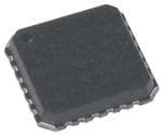
ICGOO电子元器件商城为您提供AD5760ACPZ由Analog设计生产,在icgoo商城现货销售,并且可以通过原厂、代理商等渠道进行代购。 AD5760ACPZ价格参考。AnalogAD5760ACPZ封装/规格:数据采集 - 数模转换器, 16 位 数模转换器 1 24-LFCSP-VQ(4x5)。您可以下载AD5760ACPZ参考资料、Datasheet数据手册功能说明书,资料中有AD5760ACPZ 详细功能的应用电路图电压和使用方法及教程。
AD5760ACPZ是Analog Devices Inc.(ADI)公司生产的一款高精度、16位数模转换器(DAC),广泛应用于需要高精度模拟信号输出的工业控制、仪器仪表和通信系统等领域。

该器件采用±10.8V至±16.5V双电源供电,输出电压范围宽,具有良好的线性度和稳定性,适用于对精度和稳定性要求较高的场合。其主要应用场景包括:

1. 工业自动化与过程控制:用于控制执行机构如阀门、电机等,实现高精度的模拟信号控制。
2. 测试与测量设备:如信号发生器、校准设备等,提供高精度的参考电压输出。
3. 医疗设备:用于医疗成像设备或诊断仪器中,提供稳定的模拟信号。
4. 通信系统:用于基站或光通信设备中的偏置控制和信号调节。
5. 电源管理与精密电源控制:作为高精度可调电源的核心部件。

AD5760ACPZ具备内置输出放大器和精密基准源,简化了外部电路设计,适合要求高性能和稳定性的应用环境。
| 参数 | 数值 |
| 产品目录 | 集成电路 (IC)半导体 |
| 描述 | IC DAC VOLT OUT 16BIT 24LFCSP数模转换器- DAC 16bit 2LSB buffered Ref |
| DevelopmentKit | EVAL-AD5760SDZ |
| 产品分类 | |
| 品牌 | Analog Devices Inc |
| 产品手册 | |
| 产品图片 |
|
| rohs | 符合RoHS无铅 / 符合限制有害物质指令(RoHS)规范要求 |
| 产品系列 | 数据转换器IC,数模转换器- DAC,Analog Devices AD5760ACPZ- |
| 数据手册 | |
| 产品型号 | AD5760ACPZ |
| 产品培训模块 | http://www.digikey.cn/PTM/IndividualPTM.page?site=cn&lang=zhs&ptm=26125http://www.digikey.cn/PTM/IndividualPTM.page?site=cn&lang=zhs&ptm=26140http://www.digikey.cn/PTM/IndividualPTM.page?site=cn&lang=zhs&ptm=26150http://www.digikey.cn/PTM/IndividualPTM.page?site=cn&lang=zhs&ptm=26146http://www.digikey.cn/PTM/IndividualPTM.page?site=cn&lang=zhs&ptm=26147 |
| 产品种类 | 数模转换器- DAC |
| 位数 | 16 |
| 供应商器件封装 | 24-LFCSP-VQ (4x5) |
| 分辨率 | 16 bit |
| 包装 | 托盘 |
| 商标 | Analog Devices |
| 安装类型 | 表面贴装 |
| 安装风格 | SMD/SMT |
| 封装 | Tray |
| 封装/外壳 | 24-VFQFN 裸露焊盘,CSP |
| 封装/箱体 | LFCSP-24 |
| 工作温度 | -40°C ~ 125°C |
| 工厂包装数量 | 490 |
| 建立时间 | 2.5µs |
| 接口类型 | Serial |
| 数据接口 | SPI, DSP |
| 最大工作温度 | + 125 C |
| 最小工作温度 | - 40 C |
| 标准包装 | 1 |
| 电压参考 | External |
| 电压源 | 模拟和数字,双 ± |
| 电源电压-最大 | 16.5 V |
| 电源电压-最小 | 7.5 V |
| 积分非线性 | +/- 2 LSB |
| 稳定时间 | 2.5 us |
| 系列 | AD5760 |
| 结构 | Segment |
| 转换器数 | 1 |
| 转换器数量 | 1 |
| 输出数和类型 | 1 电压 |
| 输出类型 | Voltage |
| 采样率(每秒) | - |


- 商务部:美国ITC正式对集成电路等产品启动337调查
- 曝三星4nm工艺存在良率问题 高通将骁龙8 Gen1或转产台积电
- 太阳诱电将投资9.5亿元在常州建新厂生产MLCC 预计2023年完工
- 英特尔发布欧洲新工厂建设计划 深化IDM 2.0 战略
- 台积电先进制程称霸业界 有大客户加持明年业绩稳了
- 达到5530亿美元!SIA预计今年全球半导体销售额将创下新高
- 英特尔拟将自动驾驶子公司Mobileye上市 估值或超500亿美元
- 三星加码芯片和SET,合并消费电子和移动部门,撤换高东真等 CEO
- 三星电子宣布重大人事变动 还合并消费电子和移动部门
- 海关总署:前11个月进口集成电路产品价值2.52万亿元 增长14.8%


PDF Datasheet 数据手册内容提取
Ultra Stable, 16-Bit ±0.5 LSB INL, Voltage Output DAC Data Sheet AD5760 FEATURES FUNCTIONAL BLOCK DIAGRAM True 16-bit voltage output DAC, ±0.5 LSB INL VCC VDD VREFP 8 nV/√Hz output noise spectral density 6.8kΩ 6.8kΩ 0.00625 LSB long-term linearity error stability IOVCC A1 RFB ±0.018 ppm/°C gain error temperature coefficient R1 RFB INV 23..55 nµVs -osuetcp mutid vsoclataleg gel sitecthtl iimngp tuilmsee SSCDLINK REISNGHPISIUFTTTER 16 DRAEGC 16 1D6-ABCIT VOUT SYNC AND Integrated precision reference buffers CONTROL SDO LOGIC Operating temperature range: −40°C to +125°C 6kΩ 4 mm × 5 mm LFCSP package LDAC Wide power supply range of up to ±16.5 V CLR POWER-ON RESET 31.58 M V-Hczo mScphamtiibttl et rdigiggietarel din dteigrfitaacle i nterface RESET DGNDAND CLVESASR LOGAIGCND VREFN AD5760 09650-001 APPLICATIONS Figure 1. Medical instrumentation Test and measurement Table 1. Related Devices Industrial control Part No. Description Scientific and aerospace instrumentation AD5790 20-bit, 2 LSB accurate DAC Data acquisition systems AD5791 20-bit, 1 LSB accurate DAC Digital gain and offset adjustment AD5780 18-bit, 1 LSB accurate DAC Power supply control AD5781 18-bit, 0.5 LSB INL AD5541A/AD5542A 16-bit, 1 LSB accurate 5 V DAC GENERAL DESCRIPTION The AD57601 is a true 16-bit, unbuffered voltage output digital- PRODUCT HIGHLIGHTS to-analog converter (DAC) that operates from a bipolar supply 1. True 16-bit accuracy. of up to 33 V. The AD5760 accepts a positive reference input 2. Wide power supply range of up to ±16.5 V. range of 5 V to V − 2.5 Vand a negative reference input range DD 3. −40°C to +125°C operating temperature range. of V + 2.5 V to 0 V. The AD5760 offers a relative accuracy SS 4. Low 8 nV/√Hz noise. specification of ±0.5 LSB maximum range, and operation is 5. Low ±0.018 ppm/°C gain error temperature coefficient. guaranteed monotonic with a ±0.5 LSB differential nonlinearity (DNL) maximum range specification. COMPANION PRODUCTS The device uses a versatile 3-wire serial interface that operates Output Amplifier Buffer: AD8675, ADA4898-1, ADA4004-1 at clock rates of up to 35 MHz and is compatible with standard External Reference: ADR445 serial peripheral interface (SPI), QSPI™, MICROWIRE™, and DC-to-DC Design Tool: ADIsimPower™ DSP interface standards. The device incorporates a power-on reset circuit that ensures that the DAC output powers up to 0 V Additional companion products on the AD5780 product page. in a known output impedance state and remains in this state until a valid write to the device takes place. The device provides an output clamp feature that places the output in a defined load state. 1 Protected by U.S. Patent No. 7,884,747 and 8,089,380. Rev. F Document Feedback Information furnished by Analog Devices is believed to be accurate and reliable. However, no responsibility is assumed by Analog Devices for its use, nor for any infringements of patents or other One Technology Way, P.O. Box 9106, Norwood, MA 02062-9106, U.S.A. rights of third parties that may result from its use. Specifications subject to change without notice. No license is granted by implication or otherwise under any patent or patent rights of Analog Devices. Tel: 781.329.4700 ©2011–2018 Analog Devices, Inc. All rights reserved. Trademarks and registered trademarks are the property of their respective owners. Technical Support www.analog.com
AD5760 Data Sheet TABLE OF CONTENTS Features .............................................................................................. 1 DAC Architecture ....................................................................... 18 Applications ....................................................................................... 1 Serial Interface ............................................................................ 18 Functional Block Diagram .............................................................. 1 Hardware Control Pins .............................................................. 19 General Description ......................................................................... 1 On-Chip Registers ...................................................................... 19 Product Highlights ........................................................................... 1 AD5760 Features ............................................................................ 23 Companion Products ....................................................................... 1 Power-On to 0 V ......................................................................... 23 Revision History ............................................................................... 2 Power-Up Sequence ................................................................... 23 Specifications ..................................................................................... 3 Configuring the AD5760 .......................................................... 23 Timing Characteristics ................................................................ 5 DAC Output State ...................................................................... 23 Absolute Maximum Ratings ............................................................ 7 Output Amplifier Configuration.............................................. 23 ESD Caution .................................................................................. 7 Applications Information .............................................................. 25 Pin Configuration and Function Descriptions ............................. 8 Typical Operating Circuit ......................................................... 25 Typical Performance Characteristics ............................................. 9 Evaluation Board ........................................................................ 26 Terminology .................................................................................... 17 Outline Dimensions ....................................................................... 27 Theory of Operation ...................................................................... 18 Ordering Guide .......................................................................... 27 REVISION HISTORY 4/2018—Rev. E to Rev. F 9/2012—Rev. B to Rev. C Added Power-Up Sequence Section and Figure 50; Renumbered Changes to Patent Footnote ............................................................. 1 Sequentially ..................................................................................... 23 Changes to Figure 46 ...................................................................... 17 Updated Outline Dimensions ....................................................... 27 Changes to Terminology Section ................................................. 19 Changes to Ordering Guide .......................................................... 27 Changes to Figure 53 ...................................................................... 25 Changes to Figure 55 ...................................................................... 27 10/2016—Rev. D to Rev. E Updated Outline Dimensions and changes to Changes to Figure 4 and Table 5 ..................................................... 8 Ordering Guide ............................................................................... 29 Changes to Figure 42, Figure 43, and Figure 44 ......................... 15 2/2012—Rev. A to Rev. B 7/2013—Rev. C to Rev. D Deleted Linearity Compensation Section ...................................... 3 Changes to t Test Conditions/Comments and Endnote 2 ......... 5 1 Deleted Figure 4 ................................................................................ 7 12/2011—Rev. 0 to Rev. A Changes to Pin 11 Description ....................................................... 8 Changes to Table 2 ............................................................................. 3 Deleted Daisy-Chain Operation Section ..................................... 20 Changes to Figure 48 ...................................................................... 18 Changes to DAC Register Section ................................................ 22 Changes to Table 10 and Table 11 ................................................ 23 11/2011—Revision 0: Initial Version Rev. F | Page 2 of 27
Data Sheet AD5760 SPECIFICATIONS V = +12.5 V to +16.5 V, V = −16.5 V to −12.5 V, V = +10 V, V = −10 V, V = 2.7 V to 5.5 V, IOV = 1.71 V to 5.5 V, s DD SS REFP REFN CC CC R = unloaded, C = unloaded, T to T , unless otherwise noted. L L MIN MAX Table 2. A, B Versions1 Parameter Min Typ Max Unit Test Conditions/Comments STATIC PERFORMANCE2 Resolution 16 Bits Integral Nonlinearity Error (Relative −0.5 +0.5 LSB B grade, V = ±10 V, +10 V and +5 V REFx Accuracy) −2 +2 LSB A grade, V = ±10 V, +10 V and +5 V REFx Differential Nonlinearity Error −0.5 +0.5 LSB B grade, V = ±10 V, +10 V and +5 V REFx −1 +1 LSB A grade, V = ±10 V, +10 V and +5 V REFx Long-Term Linearity Error Stability3 0.00625 LSB After 750 hours at T = 135°C A Full-Scale Error −0.75 ±0.2 +0.75 LSB V = +10 V, V = −10 V REFP REFN −1.4 ±0.17 +1.4 LSB V = 10 V, V = 0 V REFP REFN −2.5 ±0.1 +2.5 LSB V = 5 V, V = 0 V REFP REFN Full-Scale Error Temperature ±0.026 ppm/°C V = +10 V, V = −10 V REFP REFN Coefficient Zero-Scale Error −1.2 ±0.0812 +1.2 LSB V = +10 V, V = −10 V REFP REFN −2.5 ±0.044 +2.5 LSB V = 10 V, V = 0 V REFP REFN −5.2 ±0.056 +5.2 LSB V = 5 V, V = 0 V REFP REFN Zero-Scale Error Temperature ±0.025 ppm/°C V = +10 V, V = −10 V REFP REFN Coefficient Gain Error −19 ±2.3 +19 ppm FSR V = +10 V, V = −10 V REFP REFN −35 ±1.9 +35 ppm FSR V = 10 V, V = 0 V REFP REFN −68 ±0.9 +68 ppm FSR V = 5 V, V = 0 V REFP REFN Gain Error Temperature Coefficient ±0.018 ppm/°C V = +10 V, V = −10 V REFP REFN R1, R Matching 0.015 % FB OUTPUT CHARACTERISTICS Output Voltage Range V V V REFN REFP Output Voltage Settling Time 2.5 µs 10 V step to 0.02%, using the ADA4898-1 buffer in unity-gain mode 3.5 µs 125 code step to ±1 LSB4 Output Noise Spectral Density 8 nV/√Hz At 1 kHz, DAC code = midscale 8 nV/√Hz At 10 kHz, DAC code = midscale Output Voltage Noise 1.1 µV p-p DAC code = midscale, 0.1 Hz to 10 Hz bandwidth Midscale Glitch Impulse4 14 nV-sec V = +10 V, V = −10 V REFP REFN 3.5 nV-sec V = 10 V, V = 0 V REFP REFN 4 nV-sec V = 5 V, V = 0 V REFP REFN MSB Segment Glitch Impulse4 14 nV-sec V = +10 V, V = −10 V, see Figure 42 REFP REFN 3.5 nV-sec V = 10 V, V = 0 V, see Figure 43 REFP REFN 4 nV-sec V = 5 V, V = 0 V, see Figure 44 REFP REFN Output Enabled Glitch Impulse 57 nV-sec On removal of output ground clamp Digital Feedthrough 0.27 nV-sec DC Output Impedance (Normal 3.4 kΩ Mode) DC Output Impedance (Output 6 kΩ Clamped to Ground) Rev. F | Page 3 of 27
AD5760 Data Sheet A, B Versions1 Parameter Min Typ Max Unit Test Conditions/Comments REFERENCE INPUTS V Input Range 5 V − 2.5 V REFP DD V Input Range V + 2.5 0 V REFN SS Input Bias Current −20 −0.63 +20 nA −4 −0.63 +4 T = 0°C to 105°C A Input Capacitance 1 pF V , V REFP REFN LOGIC INPUTS Input Current5 −1 +1 µA Input Low Voltage, V 0.3 × IOV V IOV = 1.71 V to 5.5 V IL CC CC Input High Voltage, V 0.7 × IOV V IOV = 1.71 V to 5.5 V IH CC CC Pin Capacitance 5 pF LOGIC OUTPUT (SDO) Output Low Voltage, V 0.4 V IOV = 1.71 V to 5.5 V, sinking 1 mA OL CC Output High Voltage, V IOV − 0.5 V IOV = 1.71 V to 5.5 V, sourcing 1 mA OH CC CC High Impedance Leakage Current ±1 µA High Impedance Output 3 pF Capacitance POWER REQUIREMENTS All digital inputs at DGND or IOV CC V 7.5 V + 33 V DD SS V V − 33 −2.5 V SS DD V 2.7 5.5 V CC IOV 1.71 5.5 V IOV ≤ V CC CC CC I 10.3 14 mA DD I −10 −14 mA SS I 600 900 µA CC IOI 52 140 µA SDO disabled CC DC Power Supply Rejection Ratio ±7.5 µV/V ∆V ± 10%, V = −15 V DD SS ±1.5 µV/V ∆V ± 10%, V = 15 V SS DD AC Power Supply Rejection Ratio 90 dB ∆V ± 200 mV, 50 Hz/60 Hz, V = −15 V DD SS 90 dB ∆V ± 200 mV, 50 Hz/60 Hz, V = 15 V SS DD 1 Temperature range: −40°C to +125°C, typical conditions: TA = 25°C, VDD = +15 V, VSS = −15 V, VREFP = +10 V, VREFN = −10 V. 2 Performance characterized with the AD8675ARZ output buffer. 3 Linearity error refers to both INL error and DNL error; either parameter can be expected to drift by the amount specified after the length of time specified. 4 The AD5760 is configured in unity-gain mode with a low-pass RC filter on the output. R = 300 Ω, C = 143 pF (total capacitance seen by the output buffer, lead capacitance, and so forth). 5 Current flowing in an individual logic pin. Rev. F | Page 4 of 27
Data Sheet AD5760 TIMING CHARACTERISTICS V = 2.7 V to 5.5 V; all specifications T to T , unless otherwise noted. CC MIN MAX Table 3. Limit1 Parameter IOV = 1.71 V to 3.3 V IOV = 3.3 V to 5.5 V Unit Test Conditions/Comments CC CC t 2 40 28 ns min SCLK cycle time 1 92 60 ns min SCLK cycle time (readback mode) t 15 10 ns min SCLK high time 2 t 9 5 ns min SCLK low time 3 t 5 5 ns min SYNC to SCLK falling edge setup time 4 t 2 2 ns min SCLK falling edge to SYNC rising edge hold time 5 t 48 40 ns min Minimum SYNC high time 6 t 8 6 ns min SYNC rising edge to next SCLK falling edge ignore 7 t 9 7 ns min Data setup time 8 t 12 7 ns min Data hold time 9 t 13 10 ns min LDAC falling edge to SYNC falling edge 10 t 20 16 ns min SYNC rising edge to LDAC falling edge 11 t 14 11 ns min LDAC pulse width low 12 t 130 130 ns typ LDAC falling edge to output response time 13 t 130 130 ns typ SYNC rising edge to output response time (LDAC tied low) 14 t 50 50 ns min CLR pulse width low 15 t 140 140 ns typ CLR pulse activation time 16 t 0 0 ns min SYNC falling edge to first SCLK rising edge 17 t 65 60 ns max SYNC rising edge to SDO tristate (C = 50 pF) 18 L t 62 45 ns max SCLK rising edge to SDO valid (C = 50 pF) 19 L t 0 0 ns min SYNC rising edge to SCLK rising edge ignore 20 t 35 35 ns typ RESET pulse width low 21 t 150 150 ns typ RESET pulse activation time 22 1 All input signals are specified with tR = tF = 1 ns/V (10% to 90% of IOVCC) and timed from a voltage level of (VIL + VIH)/2. 2 Maximum SCLK frequency is 35 MHz for write mode and 16 MHz for readback mode. Rev. F | Page 5 of 27
AD5760 Data Sheet t1 SCLK 1 2 24 t6 t3 t2 t4 t5 SYNC t9 t8 SDIN DB23 DB0 t10 t11 t12 LDAC VOUT t13 VOUT t14 t15 CLR t16 VOUT t21 RESET t22 VOUT 09650-002 Figure 2. Write Mode Timing Diagram t17 t1 t7 t20 SCLK 1 2 24 1 2 24 t6 t3 t2 t4 t5 t17 t5 SYNC t9 t8 SDIN DB23 DB0 IRNEPGUITSWTEORRTDOSBPEECRIEFAIEDS NOPCONDITION t18 t19 SDO DB23 DB0 REGISTERCONTENTSCLOCKED OUT 09650-003 Figure 3. Readback Mode Timing Diagram Rev. F | Page 6 of 27
Data Sheet AD5760 ABSOLUTE MAXIMUM RATINGS T = 25°C, unless otherwise noted. Transient currents of up to A Stresses at or above those listed under Absolute Maximum 100 mA do not cause SCR latch-up. Ratings may cause permanent damage to the product. This is a stress rating only; functional operation of the product at these Table 4. or any other conditions above those indicated in the operational Parameter Rating section of this specification is not implied. Operation beyond V to AGND −0.3 V to +34 V DD the maximum operating conditions for extended periods may V to AGND −34 V to +0.3 V SS affect product reliability. V to V −0.3 V to +34 V DD SS V to DGND −0.3 V to +7 V This device is a high performance integrated circuit with an CC IOV to DGND −0.3 V to V + 3 V or +7 V ESD rating of 1.6 kV, and it is ESD sensitive. Proper precautions CC CC (whichever is less) must be taken for handling and assembly. Digital Inputs to DGND −0.3 V to IOV + 0.3 V or CC +7 V (whichever is less) V to AGND −0.3 V to V + 0.3 V ESD CAUTION OUT DD V to AGND −0.3 V to V + 0.3 V REFP DD V to AGND V − 0.3 V to +0.3 V REFN SS DGND to AGND −0.3 V to +0.3 V Operating Temperature Range, T A Industrial −40°C to +125°C Storage Temperature Range −65°C to +150°C Maximum Junction Temperature, 150°C T max J Power Dissipation (T max − T )/θ J A JA LFCSP Package θ Thermal Impedance 31.0°C/W JA Lead Temperature JEDEC industry standard Soldering J-STD-020 ESD (Human Body Model) 1.6 kV Rev. F | Page 7 of 27
AD5760 Data Sheet PIN CONFIGURATION AND FUNCTION DESCRIPTIONS INVDNCDNCDNCRFB 43210 22222 VOUT1 19 AGND VREFP 2 18VSS VDD 3 AD5760 17VSS RESET 4 TOP VIEW 16VREFN VDD 5 (Not to Scale) 15DGND CLR6 14SYNC LDAC 7 13SCLK 89101112 C CCON VCOVCDNSDSDI I NOTES 1. DNC = DO NOT CONNECT. DO NOT CONNECT TO THIS PIN. 2. NEGATIVE ANALOG SUPPLY CONNECTION (VSS). A VOLTAGE IN THE RANGE OF −16.5V TO −2.5V CAN BE CONNECTED TO THIS PIN. VSS MUST BE DECOUPLED TO AGND. 3. EXPOSED PAD. THE EXPOSED PAD CAN BE LEFT ELECTRICALLY UNCONNECTED PROVIDED THAT A SUPPLY CTCHOOAPNTPN EETRHC ETPI LOEAXNNP IEOS SFMEOADRD PEEA NADHT AB TNEHC TEEH VDES RTSHM PEAIRNLMLSYA. ILCT OPISEN RRNFEEOCCROTMEMDAM NTECONE DA.ED 09650-005 Figure 4. Pin Configuration Table 5. Pin Function Descriptions Pin No. Mnemonic Description 1 V Analog Output Voltage. OUT 2 V Positive Reference Voltage Input. A voltage in the range of 5 V to V − 2.5 V can be connected to this pin. REFP DD 3, 5 V Positive Analog Supply Connection. A voltage in the range of 7.5 V to 16.5 V can be connected to this pin. DD V must be decoupled to AGND. DD 4 RESET Active Low Reset. Asserting this pin returns the AD5760 to its power-on status. 6 CLR Active Low Input. Asserting this pin sets the DAC register to a user defined value (see Table 12) and updates the DAC output. The output value depends on the DAC register coding that is being used, either binary or twos complement. 7 LDAC Active Low Load DAC Logic Input. This pin is used to update the DAC register and, consequently, the analog output. When tied permanently low, the output is updated on the rising edge of SYNC. If LDAC is held high during the write cycle, the input register is updated, but the output update is held off until the falling edge of LDAC. Do not leave the LDAC pin unconnected. 8 V Digital Supply. Voltage range is from 2.7 V to 5.5 V. V should be decoupled to DGND. CC CC 9 IOV Digital Interface Supply. Digital threshold levels are referenced to the voltage applied to this pin. Voltage CC range is from 1.71 V to 5.5 V. 10, 21, 22, 23 DNC Do Not Connect. Do not connect to these pins. 11 SDO Serial Data Output. Data is clocked out on the rising edge of the serial clock input. 12 SDIN Serial Data Input. This device has a 24-bit input shift register. Data is clocked into the register on the falling edge of the serial clock input. 13 SCLK Serial Clock Input. Data is clocked into the input shift register on the falling edge of the serial clock input. Data can be transferred at rates of up to 35 MHz. 14 SYNC Level Triggered Control Input (Active Low). This is the frame synchronization signal for the input data. When SYNC goes low, it enables the input shift register, and data is then transferred in on the falling edges of the following clocks. The DAC is updated on the rising edge of SYNC. 15 DGND Ground Reference Pin for Digital Circuitry. 16 V Negative Reference Voltage Input. REFN 17, 18 V Negative Analog Supply Connection. A voltage in the range of −16.5 V to −2.5 V can be connected to this SS pin. V must be decoupled to AGND. SS 19 AGND Ground Reference Pin for Analog Circuitry. 20 R Feedback Connection for External Amplifier. See the AD5760 Features section for further details. FB 24 INV Inverting Input Connection for External Amplifier. See the AD5760 Features section for further details. EPAD (V ) Exposed Pad. The exposed pad can be left electrically unconnected provided that a supply connection is SS made at the V pins. It is recommended that the exposed pad be thermally connected to a copper plane for SS enhanced thermal performance. Rev. F | Page 8 of 27
Data Sheet AD5760 TYPICAL PERFORMANCE CHARACTERISTICS 0.10 0.10 00..0068 VVVVRRDSSEED FF ==PN –+==11 5+–5V11V00VV 0.05 VVVVRRDSSEED FF ==PN –+==11 5+05V5VVV 0.04 0 B)0.02 B) S S L (L 0 L (L–0.05 N N I–0.02 I –0.10 –0.04 –0.06 –0.15 –0.08 AD8675 OUTPUT BUFFER AD8675 OUTPUT BUFFER TA = 25°C TA = 25°C –0.100 10000 20000 30D0A00C CO4D00E00 50000 60000 70000 09650-006 –0.200 10000 20000 30D0A00C CO4D00E00 50000 60000 70000 09650-009 Figure 5. Integral Nonlinearity Error vs. DAC Code, ±10 V Span Figure 8. Integral Nonlinearity Error vs. DAC Code, 5 V Span, ×2 Gain Mode 0.15 0.10 0.10 VVVVRRDSSEED FF ==PN –+==11 5+05V1VV0V 00..0068 VVVVRRDSSEED FF ==PN –+==11 5+–5V11V00VV 0.04 B)0.05 B)0.02 S S NL (L NL (L 0 I 0 D–0.02 –0.04 –0.05 –0.06 AD8675 OUTPUT BUFFER –0.08 AD8675 OUTPUT BUFFER TA = 25°C TA = 25°C –0.100 10000 20000 30D0A00C CO4D00E00 50000 60000 70000 09650-007 –0.100 10000 20000 30D0A00C CO4D00E00 50000 60000 70000 09650-010 Figure 6. Integral Nonlinearity Error vs. DAC Code, 10 V Span Figure 9. Differential Nonlinearity Error vs. DAC Code, ±10 V Span 0.10 0.20 0.05 VVVVRRDSSEED FF ==PN –+==11 5+05V5VVV 0.15 VVVVRRDSSEED FF ==PN –+==11 5+05V1VV0V 0 0.10 B) B) NL (LS–0.05 NL (LS0.05 I D –0.10 0 –0.15 –0.05 AD8675 OUTPUT BUFFER AD8675 OUTPUT BUFFER TA = 25°C TA = 25°C –0.200 10000 20000 30D0A00C CO4D00E00 50000 60000 70000 09650-008 –0.100 10000 20000 30D0A00C CO4D00E00 50000 60000 70000 09650-011 Figure 7. Integral Nonlinearity Error vs. DAC Code, 5 V Span Figure 10. Differential Nonlinearity Error vs. DAC Code, 10 V Span Rev. F | Page 9 of 27
AD5760 Data Sheet 0.10 0.09 VREFP = +5V VDD = +15V 0.08 VVRDEDF =N +=1 05VV AVSDS8 6=7 –51 O5VUTPUT BUFFER VSS = –15V 0.06 0.07 0.04 DNL (LSB)–00..00220 ERROR (LSB) 00..0035 ±++1510V0VV S SSPPPAAANNN M MMAAAXXX I NIINNLLL ±++11500VVV S SSPPPAAANNN M MMINIINN I NIINNLLL L N –0.04 D –0.06 0.01 –0.08 AD8675 OUTPUT BUFFER TA = 25°C –0.100 10000 20000 30D0A00C CO4D00E00 50000 60000 70000 09650-012 –0.01–40 –20 0 TEM2P0ERATU4R0E (°C)60 80 100 09650-014 Figure 11. Differential Nonlinearity Error vs. DAC Code, 5 V Span Figure 14. Differential Nonlinearity Error vs. Temperature 0.08 AD8675 OUTPUT BUFFER INL MAX 0.09 TA = 25°C 0.06 0.07 0.04 0.05 B) 0.02 S DNL (LSB) 00..0013 L ERROR (L–0.020 AVTVARRD EE8=FF6 PN27 5 5==° CO+–11U00TVVPUT BUFFER IN–0.04 –0.01 –0.06 VREFP = +5V INL MIN –0.03 VVRDEDF =N +=1 05VV –0.08 VSS = –15V –0.050 10000 20000 30D0A00C CO4D00E00 50000 60000 70000 09650-013 –0.1.012.5 13.0 13.5 14.0VDD/1|V4S.5S| (V1)5.0 15.5 16.0 16.5 09650-016 Figure 12. Differential Nonlinearity Error vs. DAC Code, 5 V Span, Figure 15. Integral Nonlinearity Error vs. Supply Voltage, ±10 V Span ×2 Gain Mode 0.20 0.15 VDD = +15V VSS = –15V 0.15 AD8675 OUTPUT BUFFER 0.10 INL MAX 0.10 B) 0.05 B) LS LS 0.05 R ( TA = 25°C L ERROR ( 0 ±++11500VVV S SSPPPAAANNN M MMAAAXXX I NIINNLLL ±++11500VVV S SSPPPAAANNN M MMINIINN I NIINNLLL INL ERRO–0.050 VAVRRDEE8FF6PN7 5== O50VVUTPUT BUFFER N I –0.05 INL MIN –0.10 –0.10 –0.15–40 –20 0 TEM2P0ERATU4R0E (°C)60 80 100 09650-015 –0.157.5 8.5 9.5 10.5 V1D1D.5/|VSS1|2 (.V5) 13.5 14.5 15.5 16.5 09650-017 Figure 13. Integral Nonlinearity Error vs. Temperature Figure 16. Integral Nonlinearity Error vs. Supply Voltage, 5 V Span Rev. F | Page 10 of 27
Data Sheet AD5760 0.09 0.8 TA = 25°C 0.08 VREFP = 5V 0.07 DNL MAX 0.6 VARDE8F6N7 5= O0VUTPUT BUFFER B) S B) 0.06 R (L 0.4 L ERROR (LS 000...000345 TVVAARRD EE8=FF6 PN27 5 5==° OC+–11U00TVVPUT BUFFER SCALE ERRO 0.2 DN 0.02 RO- 0 E Z 0.01 –0.2 DNL MIN 0 –0.0112.5 13.0 13.5 14.0VDD/1|V4S.5S| (V)15.0 15.5 16.0 16.5 09650-018 –0.47.5 8.5 9.5 10.5 V1D1D.5/|VSS1|2 (.V5) 13.5 14.5 15.5 16.5 09650-021 Figure 17. Differential Nonlinearity Error vs. Supply Voltage, ±10 V Span Figure 20. Zero-Scale Error vs. Supply Voltage, 5 V Span 0.09 –0.02 0.08 DNL MAX –0.03 0.07 –0.04 B) SB)0.06 R (LS–0.05 L ERROR (L000...000345 TVVAARRD EE8=FF6 PN27 5 5==° OC50VVUTPUT BUFFER CALE ERRO–––000...000876 N S D D 0.02 MI–0.09 0.01 –0.10 TA = 25°C 0 DNL MIN –0.11 VVRREEFFPN == +–1100VV AD8675 OUTPUT BUFFER –0.017.5 8.5 9.5 10.5 V1D1D.5/|VSS1|2 (.V5) 13.5 14.5 15.5 16.5 09650-019 –0.1212.5 13.0 13.5 14.0VDD/1|V4S.5S| (V)15.0 15.5 16.0 16.5 09650-022 Figure 18. Differential Nonlinearity Error vs. Supply Voltage, 5 V Span Figure 21. Midscale Error vs. Supply Voltage, ±10 V Span 0.15 0.5 TA = 25°C VREFP = +10V 0.4 VREFN = –10V 0.10 AD8675 OUTPUT BUFFER 0.3 SB) B) OR (L R (LS 0.2 R 0.05 O 0.1 R R E R LE E E 0 A L SC 0 CA –0.1 ERO- MIDS –0.2 Z –0.05 –0.3 TA = 25°C –0.4 VVRREEFFPN == 50VV AD8675 OUTPUT BUFFER –0.1012.5 13.0 13.5 14.0VDD/1|V4S.5S| (V)15.0 15.5 16.0 16.5 09650-020 –0.57.5 8.5 9.5 10.5 V1D1D.5/|VSS1|2 (.V5) 13.5 14.5 15.5 16.5 09650-023 Figure 19. Zero-Scale Error vs. Supply Voltage, ±10 V Span Figure 22. Midscale Error vs. Supply Voltage, 5 V Span Rev. F | Page 11 of 27
AD5760 Data Sheet 0.14 0.38 TA = 25°C TA = 25°C VREFP = +10V VREFP = 5V 0.12 VREFN = –10V VREFN = 0V AD8675 OUTPUT BUFFER 0.36 AD8675 OUTPUT BUFFER B) LS 0.10 RROR ( 0.08 R (LSB)0.34 E O E R0.32 L R A 0.06 E ULL-SC 0.04 GAIN 0.30 F 0.02 0.28 102.5 13.0 13.5 14.0VDD/1|V4S.5S| (V)15.0 15.5 16.0 16.5 09650-024 0.267.5 8.5 9.5 10.5 V1D1D.5/|VSS1|2 (.V5) 13.5 14.5 15.5 16.5 09650-027 Figure 23. Full-Scale Error vs. Supply Voltage, ±10 V Span Figure 26. Gain Error vs. Supply Voltage, 5 V Span 0.5 0.08 TA = 25°C VREFP = 5V 0.06 INL MAX 0.3 VREFN = 0V AD8675 OUTPUT BUFFER B) 0.04 LS 0.1 R ( B) 0.02 ULL-SCALE ERRO –––000...531 INL ERROR (LS––00..00420 TVVAADSDS D8= 6= =27 5–+5°1 1OC55VUVTPUT BUFFER F –0.06 INL MIN –0.7 –0.08 –0.97.5 8.5 9.5 10.5 V1D1D.5/|VSS1|2 (.V5) 13.5 14.5 15.5 16.5 09650-025 –0.105.0 5.5 6.0 6.5 V7R.E0FP/|7V.R5EFN|8 (.0V) 8.5 9.0 9.5 10.0 09650-028 Figure 24. Full-Scale Error vs. Supply Voltage, 5 V Span Figure 27. Integral Nonlinearity Error vs. Reference Voltage 0.10 0.08 TA = 25°C VREFP = +10V 0.08 VREFN = –10V INL MAX AD8675 OUTPUT BUFFER 0.06 0.06 AIN ERROR (LSB) 00..00240 NL ERROR (LSB) 00..0024 TVVAADSDS D8= 6= =27 5–+5°1 1OC55VUVTPUT BUFFER G D –0.02 INL MIN 0 –0.04 –0.0612.5 13.0 13.5 14.0VDD/1|V4S.5S| (V)15.0 15.5 16.0 16.5 09650-026 –0.025.0 5.5 6.0 6.5 V7R.E0FP/|7V.R5EFN|8 (.0V) 8.5 9.0 9.5 10.0 09650-029 Figure 25. Gain Error vs. Supply Voltage, ±10 V Span Figure 28. Differential Nonlinearity Error vs. Reference Voltage Rev. F | Page 12 of 27
Data Sheet AD5760 –0.02 –0.25 TA = 25°C VDD = +15V –0.03 VSS = –15V AD8675 OUTPUT BUFFER –0.30 B)–0.04 S O-SCALE ERROR (L–––000...000765 GAIN ERROR (LSB) ––00..3405 R ZE–0.08 –0.45 TA = 25°C –0.09 VDD = +15V VSS = –15V AD8675 OUTPUT BUFFER –0.105.0 5.5 6.0 6.V5REF7P./0|VREF7N.5| (V)8.0 8.5 9.0 9.5 10.0 09650-030 –0.505.0 5.5 6.0 6.5 V7R.0EFP/|7V.R5EFN8| .(0V) 8.5 9.0 9.5 10.0 09650-033 Figure 29. Zero-Scale Error vs. Reference Voltage Figure 32. Gain Error vs. Reference Voltage –0.05 0.50 TA = 25°C ±10V SPAN –0.07 VDD = +15V +10V SPAN VSS = –15V 0.45 +5V SPAN AD8675 OUTPUT BUFFER –0.09 SB)–0.11 LSB) 0.40 OR (L–0.13 ROR ( 0.35 R R LE ER–0.15 ALE E 0.30 A–0.17 C C S MIDS–0.19 ULL- 0.25 F –0.21 –0.23 0.20 VVDSSD == –+1155VV AD8675 OUTPUT BUFFER –0.255.0 5.5 6.0 6.V5REF7P./0|VREF7N.5| (V)8.0 8.5 9.0 9.5 10.0 09650-031 0.15–40 –20 0 TEM2P0ERATU4R0E (°C)60 80 100 09650-034 Figure 30. Midscale Error vs. Reference Voltage Figure 33. Full-Scale Error vs. Temperature 0.40 0.15 0.38 TVVADSS D= = =2 5–+°11C55VV 0.10 ±++1150V0VV S SSPPPAAANNN AD8675 OUTPUT BUFFER ULL-SCALE ERROR (LSB)00000.....022333.682463 MIDSCALE ERROR (LSB)–––0000....110050550 F –0.20 0.24 0.22 –0.25 VVDSSD == –+1155VV AD8675 OUTPUT BUFFER 0.205.0 5.5 6.0 6.5 V7R.E0FP/|7V.R5EFN|8 (.V0) 8.5 9.0 9.5 10.0 09650-032 –0.30–40 –20 0 TEMP20ERATUR4E0 (°C) 60 80 100 09650-035 Figure 31. Full-Scale Error vs. Reference Voltage Figure 34. Midscale Error vs. Temperature Rev. F | Page 13 of 27
AD5760 Data Sheet 0.4 0.010 ±10V SPAN +10V SPAN 0.008 +5V SPAN 0.2 IDD 0.006 B) S R (L 0 0.004 O R A) 0.002 R m SCALE E –0.2 I/I (DDSS –0.0020 O- –0.4 R –0.004 E Z –0.006 –0.6 VDD = +15V ISS VSS = –15V –0.008 AD8675 OUTPUT BUFFER –0.8–40 –20 0 TEM2P0ERATU4R0E (°C)60 80 100 09650-036 –0.010–20 –15 –10 –5VDD/V0SS (V) 5 10 15 20 09650-039 Figure 35. Zero-Scale Error vs. Temperature Figure 38. Power Supply Currents vs. Power Supply Voltages 0 6 ±10V SPAN +10V SPAN –0.1 +5V SPAN 4 –0.2 2 B)–0.3 AIN ERROR (LS–––000...654 V (V)OUT ––420 VVALVVODSRRDSDEEAA FF =4D=PN 8 –+==0=11 8 15+–5-0V111VM 00BVVΩU F|F| 2E0RpEFD G –0.7 –6 –0.8 –0.9 VVDSSD == –+1155VV –8 AD8675 OUTPUT BUFFER –1.0–40 –20 0 TEM2P0ERATU4R0E (°C)60 80 100 09650-037 –10–1 0 1 TIME2 (µs) 3 4 5 09650-040 Figure 36. Gain Error vs. Temperature Figure 39. Rising Full-Scale Voltage Step 900 6 800 TA = 25°C IIIDNOOECVVCRCCRCCEE A==AS 55SIVVNIN,,G LLGOOGGIICC VVOOLLTTAAGGEE 4 VVVVDSRRSDEE FF ==PN –+==11 5+–5V11V00VV 700 IOVCC = 3V, LOGIC VOLTAGE 2 ALODAA4D8 =0 81-01M BΩU F|F| 2E0RpEFD INCREASING 600 IOVCC = 3V, LOGIC VOLTAGE DECREASING 0 OI (µA)CC540000 V (V)OUT –2 I –4 300 –6 200 100 –8 00 1 LO2GIC INPUT3 VOLTAGE4 (V) 5 6 09650-038 –10–1 0 1 TIME2 (µs) 3 4 5 09650-041 Figure 37. IOICC vs. Logic Input Voltage Figure 40. Falling Full-Scale Voltage Step Rev. F | Page 14 of 27
Data Sheet AD5760 10 6 VREFP = 5V NEGATIVE 9 VREFN = 0V POSITIVE UNITY-GAIN MODE 5 ADA4898-1 8 RC LOW-PASS FILTER 7 V-s)n 4 V) 6 CH ( m T (OUT 5 T GLI 3 V 4 PU UT 2 3 O 2 VREFP = +10V VREFN = –10V 1 1 RC LOW-PASS FILTER UNITY-GAIN MODE ADA4898-1 0–1 0 1 TIME2 (µs) 3 4 5 09650-042 0 10244096716810240133121638419456225282560028672CO31744DE34816378884096044032471045017653248563205939262464 09650-046 Figure 41. 500 Code Step Settling Time Figure 44. 6 MSB Segment Glitch Energy for 5 V VREF 25 55 VREFP = +10V NEGATIVE ±10V REF VREFN = –10V POSITIVE 10V REF UNITY-GAIN MODE 45 5V REF ADA4898-1 20 RC LOW PASS FILTER POSITIVE V-s) CONDEEG CAHTAIVNEGE CODE CHANGE mV) 35 OUTPUT GLITCH (n 1105 OUTPUT GLITCH ( 12555 –5 5 –15 01024307251207168921611264133121536017408194562150423552256002764829696C31744OD33792E35840378883993641984440324608048128501765222454272563205836860416624646451209650-044 –25–1 0 TIME1 (µs) 2 3 09650-047 Figure 42. 6 MSB Segment Glitch Energy for ±10 V VREF Figure 45. Midscale Peak-to-Peak Glitch for ±10 V 4.0 800 VREFP = 10V NEGATIVE TA = 25°C MIDSCALE CODE LOADED VREFN = 0V POSITIVE VDD = +15V OUTPUT UNBUFFERED 3.5 UNITY-GAIN MODE 600 VSS = –15V AD8676 REFERENCE BUFFERS s) 3.0 ARDCA L4O8W98-P-1ASS FILTER V) 400 VVRREEFFPN == +–1100VV H (nV- 2.5 GE (n C A 200 UTPUT GLIT 12..50 UTPUT VOLT 0 O O–200 1.0 0.5 –400 0 10244096716810240133121638419456225282560028672CO31744DE34816378884096044032471045017653248563205939262464 09650-045 –6000 1 2 3 T4IME (S5econd6s) 7 8 9 10 09650-048 Figure 43. 6 MSB Segment Glitch Energy for 10 V VRE Figure 46. Voltage Output Noise, 0.1 Hz to 10 Hz Bandwidth Rev. F | Page 15 of 27
AD5760 Data Sheet 100 0.20 VDD = +15V VDD = +15V VSS = –15V 0.18 VSS = –15V VREFP = +10V VREFP = +10V VREFN = –10V 0.16 VREFN = –10V UNITY GAIN ADA4898-1 V)0.14 Hz) AGE (0.12 D (nV/√ 10 T VOLT00..1008 S U N TP0.06 U O 0.04 0.02 0 10.1 1 FR10EQUENCY 1(H00z) 1k 10k 09650-056 –0.020 1 2 TIME3 (µs) 4 5 6 09650-049 Figure 47. Noise Spectral Density vs. Frequency Figure 48. Glitch Impulse on Removal of Output Clamp Rev. F | Page 16 of 27
Data Sheet AD5760 TERMINOLOGY Relative Accuracy Output Voltage Settling Time Relative accuracy, or integral nonlinearity (INL), is a measure of Output voltage settling time is the amount of time it takes for the maximum deviation, in LSB, from a straight line passing the output voltage to settle to a specified level for a specified through the endpoints of the DAC transfer function. A typical change in voltage. For fast settling applications, a high speed INL error vs. code plot is shown in Figure 5. buffer amplifier is required to buffer the load from the 3.4 kΩ output impedance of the AD5760, in which case, it is the Differential Nonlinearity (DNL) amplifier that determines the settling time. Differential nonlinearity is the difference between the measured change and the ideal 1 LSB change between any two adjacent Digital-to-Analog Glitch Impulse codes. A specified differential nonlinearity of ±1 LSB maximum Digital-to-analog glitch impulse is the impulse injected into the ensures monotonicity. This DAC is guaranteed monotonic. A analog output when the input code in the DAC register changes typical DNL error vs. code plot is shown in Figure 9. state. It is specified as the area of the glitch in nV-sec and is measured when the digital input code is changed by 1 LSB at Linearity Error Long-Term Stability the major carry transition (see Figure 48). Linearity error long-term stability is a measure of the stability of the linearity of the DAC over a long period of time. It is specified Output Enabled Glitch Impulse in LSB for a time period of 500 hours and 1000 hours at an Output enabled glitch impulse is the impulse injected into the elevated ambient temperature. analog output when the clamp to ground on the DAC output is removed. It is specified as the area of the glitch in nV-sec (see Zero-Scale Error Figure 48). Zero-scale error is a measure of the output error when zero-scale code (0x00000) is loaded to the DAC register. Ideally, the output Digital Feedthrough voltage should be VREFN. Zero-scale error is expressed in LSBs. Digital feedthrough is a measure of the impulse injected into the analog output of the DAC from the digital inputs of the Zero-Scale Error Temperature Coefficient DAC but is measured when the DAC output is not updated. It is Zero-scale error temperature coefficient is a measure of the specified in nV-sec and measured with a full-scale code change change in zero-scale error with a change in temperature. It is on the data bus, that is, from all 0s to all 1s, and vice versa. expressed in ppm FSR/°C. Total Harmonic Distortion (THD) Full-Scale Error Total harmonic distortion is the ratio of the rms sum of the Full-scale error is a measure of the output error when full-scale harmonics of the DAC output to the fundamental value. Only code (0x0FFFF) is loaded to the DAC register. Ideally, the the second to fifth harmonics are included. output voltage should be V − 1 LSB. Full-scale error is REFP expressed in LSBs. DC Power Supply Rejection Ratio. DC power supply rejection ratio is a measure of the rejection of Full-Scale Error Temperature Coefficient the output voltage to dc changes in the power supplies applied Full-scale error temperature coefficient is a measure of the to the DAC. It is measured for a given dc change in power change in full-scale error with a change in temperature. It is supply voltage and is expressed in µV/V. expressed in ppm FSR/°C. AC Power Supply Rejection Ratio (AC PSRR) Gain Error AC power supply rejection ratio is a measure of the rejection of Gain error is a measure of the span error of the DAC. It is the the output voltage to ac changes in the power supplies applied deviation in slope of the DAC transfer characteristic from the to the DAC. It is measured for a given amplitude and frequency ideal, expressed in ppm of the full-scale range. change in power supply voltage and is expressed in decibels. Gain Error Temperature Coefficient Gain error temperature coefficient is a measure of the change in gain error with a change in temperature. It is expressed in ppm FSR/°C. Midscale Error Midscale error is a measure of the output error when midscale code (0x08000) is loaded to the DAC register. Ideally, the output voltage should be (V – V )/2 +V . Midscale error is REFP REFN REFN expressed in LSBs. Rev. F | Page 17 of 27
AD5760 Data Sheet THEORY OF OPERATION The AD5760 is a high accuracy, fast settling, single, 16-bit, R R R VOUT serial input, voltage output DAC. It operates from a VDD supply 2R 2R 2R... 2R 2R 2R... 2R voltage of 7.5 V to 16.5 V and a VSS supply of −16.5 V to −2.5 V. VREFP S0 S1... S9 E62 E61... E0 Data is written to the AD5760 in a 24-bit word format via a 3-wire serial interface. The AD5760 incorporates a power-on reset circuit that ensures the DAC output powers up to 0 V with the DVOAUTC p AinR cClaHmIpTeEdC toT UAGRNE D through a ~6 kΩ internal resistor. VREFN 10-BITR-2RLADDER SI6X3MESQBUsADLESCEOGDMEEDN ITNSTO 09650-050 Figure 49. DAC Ladder Structure Serial Interface The architecture of the AD5760 consists of two matched DAC SERIAL INTERFACE sections. A simplified circuit diagram is shown in Figure 49. The six MSBs of the 16-bit data-word are decoded to drive The AD5760 has a 3-wire serial interface (SYNC, SCLK, and 63 switches, E0 to E62. Each of these switches connects one of SDIN) that is compatible with SPI, QSPI, and MICROWIRE 63 matched resistors to either the buffered V or buffered interface standards, as well as most DSPs (see Figure 2 for a REFP V voltage. The remaining 10 bits of the data-word drive the timing diagram). REFN S0 to S9 switches of a 10-bit voltage mode R-2R ladder network. Input Shift Register The input shift register is 24 bits wide. Data is loaded into the device MSB first as a 24-bit word under the control of a serial clock input, SCLK, which can operate at up to 35 MHz. The input register consists of a R/W bit, three address bits, and 20 data bits as shown in Table 6. The timing diagram for this operation is shown in Figure 2. Table 6. Input Shift Register Format MSB LSB DB23 DB22 DB21 DB20 DB19 to DB0 R/W Register address Register data Table 7. Decoding the Input Shift Register R/W Register Address Description X1 0 0 0 No operation (NOP). Used in readback operations. 0 0 0 1 Write to the DAC register. 0 0 1 0 Write to the control register. 0 0 1 1 Write to the clearcode register. 0 1 0 0 Write to the software control register. 1 0 0 1 Read from the DAC register. 1 0 1 0 Read from the control register. 1 0 1 1 Read from the clearcode register. 1 X is don’t care. Rev. F | Page 18 of 27
Data Sheet AD5760 Standalone Operation Synchronous DAC Update The serial interface works with both a continuous and noncon- In this mode, LDAC is held low while data is being clocked into tinuous serial clock. A continuous SCLK source can be used the input shift register. The DAC output is updated on the rising only if SYNC is held low for the correct number of clock cycles. edge of SYNC. In gated clock mode, a burst clock containing the exact number Asynchronous DAC Update of clock cycles must be used, and SYNC must be taken high after In this mode, LDAC is held high while data is being clocked the final clock to latch the data. The first falling edge of SYNC into the input shift register. The DAC output is asynchronously starts the write cycle. Exactly 24 falling clock edges must be applied updated by taking LDAC low after SYNC has been taken high. to SCLK before SYNC is brought high again. If SYNC is brought The update now occurs on the falling edge of LDAC. high before the 24th falling SCLK edge, the data written is invalid. If more than 24 falling SCLK edges are applied before SYNC is Reset Function (RESET) brought high, the input data is also invalid. The AD5760 can be reset to its power-on state by two means: The input shift register is updated on the rising edge of SYNC. either by asserting the RESET pin or by using the reset function For another serial transfer to take place, SYNC must be brought in the software control register (see Table 13). If the RESET pin low again. After the end of the serial data transfer, data is is not used, hardwire it to IOVCC. automatically transferred from the input shift register to the Asynchronous Clear Function (CLR) addressed register. When the write cycle is complete, the output The CLR pin is an active low clear that allows the output to be can be updated by taking LDAC low while SYNC is high. cleared to a user defined value. The 16-bit clearcode value is Readback programmed to the clearcode register (see Table 12). It is The contents of all the on-chip registers can be read back via the necessary to maintain CLR low for a minimum amount of time SDO pin. Table 7 outlines how the registers are decoded. After a to complete the operation (see Figure 2). When the CLR signal register has been addressed for a read, the next 24 clock cycles is returned high, the output remains at the clear value (if LDAC clock the data out on the SDO pin. The clocks must be applied is high) until a new value is loaded to the DAC register. The while SYNC is low. When SYNC is returned high, the SDO pin output cannot be updated with a new value while the CLR pin is is placed in tristate. For a read of a single register, the NOP low. A clear operation can also be performed by setting the CLR function can be used to clock out the data. Alternatively, if more bit in the software control register (see Table 13). than one register is to be read, the data of the first register to be ON-CHIP REGISTERS addressed can be clocked out at the same time that the second DAC Register register to be read is being addressed. The SDO pin must be enabled to complete a readback operation. The SDO pin is Table 9 outlines how data is written to and read from the DAC enabled by default. register. HARDWARE CONTROL PINS The following equation describes the ideal transfer function of Load DAC Function (LDAC) the DAC: After data has been transferred into the input register of the V = (VREFP −VREFN)×D +V DAC, there are two ways to update the DAC register and DAC OUT 216 REFN output. Depending on the status of both SYNC and LDAC, one where: of two update modes is selected: synchronous DAC update or V is the negative voltage applied at the V input pin. REFN REFN asynchronous DAC update. V is the positive voltage applied at the V input pin. REFP REFP D is the 16-bit code programmed to the DAC. Rev. F | Page 19 of 27
AD5760 Data Sheet Table 8. Hardware Control Pins Truth Table LDAC CLR RESET Function X1 X1 0 The AD5760 is in reset mode. The device cannot be programmed. X1 X1 The AD5760 is returned to its power-on state. All registers are set to their default values. 0 0 1 The DAC register is loaded with the clearcode register value, and the output is set accordingly. 0 1 1 The output is set according to the DAC register value. 1 0 1 The DAC register is loaded with the clearcode register value, and the output is set accordingly. 1 1 The output is set according to the DAC register value. 0 1 The output remains at the clearcode register value. 1 1 The output remains set according to the DAC register value. 0 1 The output remains at the clearcode register value. 1 1 The DAC register is loaded with the clearcode register value and the output is set accordingly. 0 1 The DAC register is loaded with the clearcode register value and the output is set accordingly. 1 1 The output remains at the clearcode register value. 0 1 The output is set according to the DAC register value. 1 X is don’t care. Table 9. DAC Register MSB LSB DB23 DB22 DB21 DB20 DB19 to DB4 DB3 DB2 DB1 DB0 R/W Register address DAC register data R/W 0 0 1 16 bits of data X1 X1 X1 X1 1 X is don’t care. Rev. F | Page 20 of 27
Data Sheet AD5760 Control Register Clearcode Register The control register controls the mode of operation of the The clearcode register sets the value to which the DAC output is AD5760. set when the CLR pin or CLR bit in the software control register is asserted. The output value depends on the DAC coding that is being used, either binary or twos complement. The default register value is 0. Table 10. Control Register MSB LSB DB23 DB22 DB21 DB20 DB19 to DB11 DB10 DB9 DB8 DB7 DB6 DB5 DB4 DB3 DB2 DB1 DB0 R/W Register address Control register data R/W 0 1 0 Reserved Reserved 0000 SDODIS BIN/2sC DACTRI OPGND RBUF Reserved Table 11. Control Register Functions Bit Name Description Reserved These bits are reserved and should be programmed to zero. RBUF Output amplifier configuration control. 0: the internal amplifier, A1, is powered up and Resistors R and R1 are connected in series, as shown in Figure 53. This allows FB an external amplifier to be connected in a gain of two configuration. See the AD5760 Features section for further details. 1: (default) the internal amplifier, A1, is powered down and Resistors R and R1 are connected in parallel, as shown in FB Figure 52, so that the resistance between the RFB and INV pins is 3.4 kΩ, equal to the resistance of the DAC. This allows the R FB and INV pins to be used for input bias current compensation for an external unity-gain amplifier. See the AD5760 Features section for further details. OPGND Output ground clamp control. 0: the DAC output clamp to ground is removed, and the DAC is placed in normal mode. 1: (default) the DAC output is clamped to ground through a ~6 kΩ resistance, and the DAC is placed in tristate mode. Resetting the device puts the DAC in OPGND mode, where the output ground clamp is enabled and the DAC is tristated. Setting the OPGND bit to 1 in the control register overrules any write to the DACTRI bit. DACTRI DAC tristate control. 0: the DAC is in normal operating mode. 1: (default) the DAC is in tristate mode. BIN/2sC DAC register coding selection. 0: (default) the DAC register uses twos complement coding. 1: the DAC register uses offset binary coding. SDODIS SDO pin enable/disable control. 0: (default) the SDO pin is enabled. 1: the SDO pin is disabled (tristate). R/W Read/write select bit. 0: AD5760 is addressed for a write operation. 1: AD5760 is addressed for a read operation. Table 12. Clearcode Register MSB LSB DB23 DB22 DB21 DB20 DB19 to DB4 DB3 DB2 DB1 DB0 R/W Register address Clearcode register data R/W 0 1 1 16 bits of data X1 X1 X1 X1 1 X is don’t care. Rev. F | Page 21 of 27
AD5760 Data Sheet Software Control Register This is a write only register in which writing a 1 to a particular bit has the same effect as pulsing the corresponding pin low. Table 13. Software Control Register MSB LSB DB23 DB22 DB21 DB20 DB19 to DB3 DB2 DB1 DB0 R/W Register address Software control register data 0 1 0 0 Reserved Reset CLR1 LDAC2 1 The CLR function has no effect when the LDAC pin is low. 2 The LDAC function has no effect when the CLR pin is low. Table 14. Software Control Register Functions Bit Name Description LDAC Setting this bit to 1 updates the DAC register and, consequently, the DAC output. CLR Setting this bit to 1 sets the DAC register to a user defined value (see Table 12) and updates the DAC output. The output value depends on the DAC register coding that is being used, either binary or twos complement. Reset Setting this bit to 1 returns the AD5760 to its power-on state. Rev. F | Page 22 of 27
Data Sheet AD5760 AD5760 FEATURES POWER-ON TO 0 V OUTPUT AMPLIFIER CONFIGURATION The AD5760 contains a power-on reset circuit that, as well as There are a number of different ways that an output amplifier resetting all registers to their default values, controls the output can be connected to the AD5760, depending on the voltage voltage during power-up. Upon power-on, the DAC is placed in references applied and the desired output voltage span. tristate (its reference inputs are disconnected), and its output is Unity-Gain Configuration clamped to AGND through a ~6 kΩ resistor. The DAC remains Figure 51 shows an output amplifier configured for unity gain. in this state until programmed otherwise via the control register. In this configuration, the output spans from V to V . This is a useful feature in applications where it is important to REFN REFP know the state of the DAC output while it is in the process of VREFP powering up. 6.8kΩ 6.8kΩ RFB POWER-UP SEQUENCE A1 R1 RFB INV ADAAD48869785-1 To power up the device in a known safe state, power up the VDD ADA4004-1 supply before powering up the V supply. This step ensures 16-BIT VOUT CC DAC VOUT that V does not come up while V is unpowered during CC DD power-on. If the device cannot be powered-up in a safe state, csuopnpnleiecst aans sehxotewrnn ailn S Fcihgoutrtek y5 0d.i ode across the VDD and VCC VREFN AD5760 09650-052 VCC VDD Figure 51. Output Amplifier in Unity-Gain Configuration A second unity-gain configuration for the output amplifier is one that removes an offset from the input bias currents of the VCC VDD amplifier. It does this by inserting a resistance in the feedback path of the amplifier that is equal to the output resistance of the AD5760 DAC. The DAC output resistance is 3.4 kΩ. By connecting R1 09650-150 aavnadi lRabFBl ei no np acrhailple. lB, ae craeusisset atnhec er eesqiustaolr tso a trhee a Dll AonC ornesei sptiaenccee o ifs Figure 50. Schottky Diode Connection silicon, they are temperature coefficient matched. To enable this CONFIGURING THE AD5760 mode of operation, the RBUF bit of the control register must be After power-on, the AD5760 must be configured to put it into set to Logic 1. Figure 52 shows how the output amplifier is normal operating mode before programming the output. To connected to the AD5760. In this configuration, the output do this, the control register must be programmed. The DAC amplifier is in unity gain, and the output spans from VREFN to is removed from tristate by clearing the DACTRI bit, and the VREFP. This unity-gain configuration allows a capacitor to be output clamp is removed by clearing the OPGND bit. At this placed in the amplifier feedback path to improve dynamic point, the output goes to V unless an alternative value is performance. REFN first programmed to the DAC register. VREFP DAC OUTPUT STATE RFB The DAC output can be placed in one of three states, controlled R1 RFB 10pF 6.8kΩ 6.8kΩ INV by the DACTRI and OPGND bits of the control register, as shown in Table 15. 16-BIT VOUT VOUT DAC AD8675 Table 15. Output State Truth Table ADA4898-1 ADA4004-1 DACTRI OPGND Output State 00 01 NOourtmpuatl iosp celarmatipnegd m vioad ~e6. kΩ to AGND. VREFN AD5760 09650-053 1 0 Output is in tristate. Figure 52. Output Amplifier in Unity-Gain with Amplifier Input Bias Current Compensation 1 1 Output is clamped via ~6 kΩ to AGND. Rev. F | Page 23 of 27
AD5760 Data Sheet Gain of Two Configuration (×2 Gain Mode) VREFP Figure 53 shows an output amplifier configured for a gain of two. The gain is set by the internal matched 6.8 kΩ resistors, A1 6.8kΩ 6.8kΩ RFB which are exactly twice the DAC resistance, having the effect R1 RFB INV 10pF of removing an offset from the input bias current of the external 16-BIT VOUT VOUT amplifier. In this configuration, the output spans from 2 × V − DAC REFN AD8675 V to V . This configuration is used to generate a bipolar ADA4898-1 REFP REFP ADA4004-1 output span from a single-ended reference input, with V = REFN 0re Vgi. sFteorr mthuiss tm boed cele oafr eodp etora Ltioogni,c t 0h.e RBUF bit of the control VREFN AD5760 09650-054 Figure 53. Output Amplifier in Gain of Two Configuration Rev. F | Page 24 of 27
Data Sheet AD5760 APPLICATIONS INFORMATION TYPICAL OPERATING CIRCUIT 550-05690 Figure 54. Typical Operating Circuit Rev. F | Page 25 of 27
AD5760 Data Sheet Figure 54 shows a typical operating circuit for the AD5760 to aid designers in evaluating the high performance of the device using an AD8675 as an output buffer. Because the output with minimum effort. The evaluation kit includes a populated impedance of the AD5760 is 3.4 kΩ, an output buffer is and tested AD5780 printed circuit board (PCB). The evaluation required for driving low resistive, high capacitive loads. board interfaces to the USB port of a PC. Software is available EVALUATION BOARD with the evaluation board to allow the user to easily program the AD5780. The software runs on any PC that has Microsoft® Refer to the evaluation board available for the AD5780 or Windows® XP (SP2), Vista (32-bit or 64-bit), or Windows 7 AD5790 to evaluate a 18-bit version or 20-bit version of the installed. The UG-256 is available, which gives full details on AD5760. An evaluation board is available for the AD5780 the operation of the evaluation board Rev. F | Page 26 of 27
Data Sheet AD5760 OUTLINE DIMENSIONS DETAIL A (JEDEC 95) 4.10 2.75 4.00 2.65 PIN 1 3.90 2.50 INDICATOR PININD I1CATOR AREA OPTIONS 20 24 (SEE DETAIL A) 19 1 0.50 5.10 BSC 3.75 5.00 EXPPAODSED 3.65 4.90 3.50 13 7 0.50 12 8 TOP VIEW BOTTOM VIEW 0.40 1.00 0.30 0.90 SIDE VIEW 0.05 MAX FOR PROPER CONNECTION OF 0.80 THE EXPOSED PAD, REFER TO 0.02 NOM THE PIN CONFIGURATION AND COPLANARITY FUNCTION DESCRIPTIONS SEATING 0.30 0.08 SECTION OF THIS DATA SHEET. PKG-003573 PLANE 00..2250 0.20 REF 08-18-2017-B Figure 55. 24-Lead Lead Frame Chip Scale Package [LFCSP] 4 mm × 5 mm Body and 0.90 mm Package Height (CP-24-5) Dimensions shown in millimeters ORDERING GUIDE Model1 Temperature Range INL Package Description Package Option AD5760BCPZ −40°C to +125°C ±0.5 LSB 24-Lead Lead Frame Chip Scale Package [LFCSP] CP-24-5 AD5760BCPZ-REEL7 −40°C to +125°C ±0.5 LSB 24-Lead Lead Frame Chip Scale Package [LFCSP] CP-24-5 AD5760ACPZ −40°C to +125°C ±2 LSB 24-Lead Lead Frame Chip Scale Package [LFCSP] CP-24-5 AD5760ACPZ-REEL7 −40°C to +125°C ±2 LSB 24-Lead Lead Frame Chip Scale Package [LFCSP] CP-24-5 EVAL-AD5760SDZ Evaluation Board 1 Z = RoHS Compliant Part. ©2011–2018 Analog Devices, Inc. All rights reserved. Trademarks and registered trademarks are the property of their respective owners. D09650-0-4/18(F) Rev. F | Page 27 of 27
Mouser Electronics Authorized Distributor Click to View Pricing, Inventory, Delivery & Lifecycle Information: A nalog Devices Inc.: EVAL-AD5760SDZ AD5760BCPZ-REEL7 AD5760ACPZ AD5760ACPZ-REEL7 AD5760BCPZ