ICGOO在线商城 > 集成电路(IC) > 数据采集 - 数模转换器 > AD5063BRMZ-1
 Datasheet下载
- 型号: AD5063BRMZ-1
- 制造商: Analog
- 库位|库存: xxxx|xxxx
- 要求:
| 数量阶梯 | 香港交货 | 国内含税 |
| +xxxx | $xxxx | ¥xxxx |
查看当月历史价格
查看今年历史价格
AD5063BRMZ-1产品简介:
ICGOO电子元器件商城为您提供AD5063BRMZ-1由Analog设计生产,在icgoo商城现货销售,并且可以通过原厂、代理商等渠道进行代购。 AD5063BRMZ-1价格参考。AnalogAD5063BRMZ-1封装/规格:数据采集 - 数模转换器, 16 位 数模转换器 1 10-MSOP。您可以下载AD5063BRMZ-1参考资料、Datasheet数据手册功能说明书,资料中有AD5063BRMZ-1 详细功能的应用电路图电压和使用方法及教程。
AD5063BRMZ-1 是由 Analog Devices Inc. 生产的一款高精度、低功耗的数模转换器(DAC),广泛应用于需要精确控制和信号处理的场合。以下是其主要应用场景:

 1. 工业自动化与控制系统
AD5063BRMZ-1 可用于工业自动化中的精密控制,如温度、压力、流量等传感器数据的采集与反馈控制。它能够将数字信号转换为模拟信号,驱动执行器或调节器,确保系统的稳定性和精度。例如,在智能工厂中,该器件可以用于调节电机的速度或位置,实现精准的运动控制。

 2. 仪器仪表
在精密测量仪器中,AD5063BRMZ-1 可以用于生成高精度的参考电压或电流源,帮助提高测量的准确性。它适用于电子测试设备、医疗仪器、环境监测设备等场景,确保信号的稳定性和可靠性。

 3. 通信系统
在通信领域,AD5063BRMZ-1 可用于生成调制信号或偏置电压,特别是在射频(RF)和微波通信系统中。它能够提供稳定的模拟输出,确保信号的高质量传输和接收。

 4. 音频处理
AD5063BRMZ-1 还适用于音频处理设备,如专业音响系统、录音设备等。它可以将数字音频信号转换为模拟信号,提供高质量的声音输出,满足高保真音频应用的需求。

 5. 汽车电子
在汽车电子系统中,AD5063BRMZ-1 可用于发动机控制单元(ECU)、车身控制系统等,提供精确的信号控制。例如,它可以帮助调节燃油喷射量、点火正时等关键参数,提升车辆的性能和燃油效率。

 6. 医疗设备
在医疗设备中,AD5063BRMZ-1 可用于生成精确的控制信号,如在心电图(ECG)、超声波成像等设备中,确保信号的准确性和稳定性,保障诊断结果的可靠性。

总之,AD5063BRMZ-1 凭借其高精度、低功耗的特点,适用于多种对信号质量要求较高的应用场景,尤其适合那些需要精确控制和稳定输出的系统。
| 参数 | 数值 |
| 产品目录 | 集成电路 (IC)半导体 |
| 描述 | IC DAC 16BIT 2.7-5.5V 10MSOP数模转换器- DAC IC 16-Bit VOUT |
| 产品分类 | |
| 品牌 | Analog Devices |
| 产品手册 | |
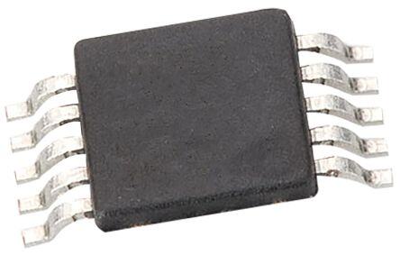
| 产品图片 |
|
| rohs | 符合RoHS无铅 / 符合限制有害物质指令(RoHS)规范要求 |
| 产品系列 | 数据转换器IC,数模转换器- DAC,Analog Devices AD5063BRMZ-1nanoDAC™ |
| 数据手册 | |
| 产品型号 | AD5063BRMZ-1 |
| 产品培训模块 | http://www.digikey.cn/PTM/IndividualPTM.page?site=cn&lang=zhs&ptm=26125http://www.digikey.cn/PTM/IndividualPTM.page?site=cn&lang=zhs&ptm=26140http://www.digikey.cn/PTM/IndividualPTM.page?site=cn&lang=zhs&ptm=26150http://www.digikey.cn/PTM/IndividualPTM.page?site=cn&lang=zhs&ptm=26147 |
| 产品目录页面 | |
| 产品种类 | 数模转换器- DAC |
| 位数 | 16 |
| 供应商器件封装 | 10-MSOP |
| 其它名称 | AD5063BRMZ1 |
| 分辨率 | 16 bit |
| 包装 | 管件 |
| 商标 | Analog Devices |
| 安装类型 | 表面贴装 |
| 安装风格 | SMD/SMT |
| 封装 | Tube |
| 封装/外壳 | 10-TFSOP,10-MSOP(0.118",3.00mm 宽) |
| 封装/箱体 | MSOP-10 |
| 工作温度 | -40°C ~ 85°C |
| 工厂包装数量 | 50 |
| 建立时间 | 1µs |
| 接口类型 | SPI |
| 数据接口 | SPI |
| 最大功率耗散 | 3.85 mW |
| 最大工作温度 | + 125 C |
| 最小工作温度 | - 40 C |
| 标准包装 | 50 |
| 电压参考 | External |
| 电压源 | 单电源 |
| 电源电压-最大 | 5.5 V |
| 电源电压-最小 | 2.7 V |
| 积分非线性 | +/- 1 LSB |
| 稳定时间 | 4 us |
| 系列 | AD5063 |
| 结构 | R-2R |
| 转换器数 | 1 |
| 转换器数量 | 1 |
| 输出数和类型 | 1 电压,单极1 电压,双极 |
| 输出类型 | Voltage |
| 采样比 | 333 kSPs |
| 采样率(每秒) | 333k |


- 商务部:美国ITC正式对集成电路等产品启动337调查
- 曝三星4nm工艺存在良率问题 高通将骁龙8 Gen1或转产台积电
- 太阳诱电将投资9.5亿元在常州建新厂生产MLCC 预计2023年完工
- 英特尔发布欧洲新工厂建设计划 深化IDM 2.0 战略
- 台积电先进制程称霸业界 有大客户加持明年业绩稳了
- 达到5530亿美元!SIA预计今年全球半导体销售额将创下新高
- 英特尔拟将自动驾驶子公司Mobileye上市 估值或超500亿美元
- 三星加码芯片和SET,合并消费电子和移动部门,撤换高东真等 CEO
- 三星电子宣布重大人事变动 还合并消费电子和移动部门
- 海关总署:前11个月进口集成电路产品价值2.52万亿元 增长14.8%


PDF Datasheet 数据手册内容提取
Fully Accurate 16-Bit V nanoDAC OUT SPI Interface 2.7 V to 5.5 V in an MSOP Data Sheet AD5063 FEATURES FUNCTIONAL BLOCK DIAGRAM Single 16-bit DAC, 1 LSB INL VREF VDD Power-on reset to midscale Guaranteed monotonic by design PORWEESRE-TON BUF AD5063 RFB 3 power-down functions INV Low power serial interface with Schmitt-triggered inputs REF(+) 10-lead MSOP, low power REGDIASCTER DAC VOUT Fast settling time of 1 µs maximum (AD5063-1 model) 2.7 V to 5.5 V power supply Low glitch on power-up AGND INPUT POWER-DOWN Unbuffered voltage capable of driving 60 kΩ load CONTROL CONTROL LOGIC RESISTOR LOGIC NETWORK SYNC interrupt facility APPLICATIONS 04766-001 SYNC SCLK DIN DACGND Process control Figure 1. Data acquisition systems Portable battery-powered instruments Digital gain and offset adjustment Programmable voltage and current sources Programmable attenuators GENERAL DESCRIPTION PRODUCT HIGHLIGHTS The AD5063, a member of the Analog Device Inc., nanoDAC™ family, is a low power, single 16-bit, unbuffered voltage-output 1. Available in 10-lead MSOP. DAC that operates from a single 2.7 V to 5 V supply. The device 2. 16-bit accurate, 1 LSB INL. offers a relative accuracy specification of ±1 LSB, and operation 3. Low glitch on power-up. is guaranteed monotonic with a ±1 LSB DNL specification. The 4. High speed serial interface with clock speeds up to 30 MHz. AD5063 comes with on-board resistors in a 10-lead MSOP, 5. Three power-down modes available to the user. allowing bipolar signals to be generated with an output amplifier. The device uses a versatile 3-wire serial interface that operates Table 1. Related Devices at clock rates up to 30 MHz and that is compatible with Part No. Description standard SPI®, QSPI™, MICROWIRE™, and DSP interface AD5061 2.7 V to 5.5 V, 16-bit nanoDAC D/A, standards. The reference for the AD5063 is supplied from an 4 LSBs INL, SOT-23. external V pin. A reference buffer is also provided on-chip. REF AD5062 2.7 V to 5.5 V, 16-bit nanoDAC D/A, The device incorporates a power-on reset circuit that ensures 1 LSB INL, SOT-23. the DAC output powers up to midscale and remains there until AD5040/AD5060 2.7 V to 5.5 V, 14-/16-bit nanoDAC D/A, a valid write to the device takes place. The device contains a 1 LSB INL, SOT-23. power-down feature that reduces the current consumption of the device to typically 300 nA at 5 V and provides software- selectable output loads while in power-down mode. The device is put into power-down mode via the serial interface. Total unadjusted error for the device is <1 mV. This device exhibits very low glitch on power-up. Rev. D Document Feedback Information furnished by Analog Devices is believed to be accurate and reliable. However, no responsibility is assumed by Analog Devices for its use, nor for any infringements of patents or other One Technology Way, P.O. Box 9106, Norwood, MA 02062-9106, U.S.A. rights of third parties that may result from its use. Specifications subject to change without notice. No license is granted by implication or otherwise under any patent or patent rights of Analog Devices. Tel: 781.329.4700 ©2005–2018 Analog Devices, Inc. All rights reserved. Trademarks and registered trademarks are the property of their respective owners. Technical Support www.analog.com
AD5063 Data Sheet TABLE OF CONTENTS Features .............................................................................................. 1 Serial Interface ............................................................................ 13 Applications ....................................................................................... 1 Input Shift Register .................................................................... 13 Functional Block Diagram .............................................................. 1 SYNC Interrupt .......................................................................... 13 General Description ......................................................................... 1 Power-On to Midscale ............................................................... 14 Product Highlights ........................................................................... 1 Software Reset ............................................................................. 14 Revision History ............................................................................... 2 Power-Down Modes .................................................................. 14 Specifications ..................................................................................... 3 Microprocessor Interfacing ....................................................... 14 Timing Characteristics ................................................................ 5 Applications Information .............................................................. 16 Absolute Maximum Ratings ............................................................ 6 Choosing a Reference for the AD5063 .................................... 16 ESD Caution .................................................................................. 6 Bipolar Operation Using the AD5063 ..................................... 16 Pin Configuration and Function Descriptions ............................. 7 Using the AD5063 with a Galvanically Isolated Interface Chip .............................................................................................. 17 Typical Performance Characteristics ............................................. 8 Power Supply Bypassing and Grounding ................................ 17 Terminology .................................................................................... 12 Outline Dimensions ....................................................................... 18 Theory of Operation ...................................................................... 13 Ordering Guide .......................................................................... 18 DAC Architecture ....................................................................... 13 Reference Buffer ......................................................................... 13 REVISION HISTORY Change to Serial Interface Section ............................................... 13 4/2018—Rev. C to Rev. D Change to Table 6 ........................................................................... 14 Changed Application Section to Applications Information Change to Bipolar Operation Using the AD5063 Section ........ 16 Section .............................................................................................. 16 Changes to Bipolar Operation Using the AD5063 Section and 7/2005—Rev. 0 to Rev. A Figure 37 .......................................................................................... 16 Changes to Galvanically Isolated Chip Section .......................... 17 Changes to Ordering Guide .......................................................... 18 Changes to Figure 38 ...................................................................... 17 8/2009—Rev. B to Rev. C 4/2005—Revision 0: Initial Version Changes to Features Section............................................................ 1 Changes to Output Voltage Settling Time Parameter, Table 2 ... 3 Updated Outline Dimensions ....................................................... 18 Changes to Ordering Guide .......................................................... 18 3/2006—Rev. A to Rev. B Updated Format .................................................................. Universal Change to Features ........................................................................... 1 Change to Figure 1 ........................................................................... 1 Changes to Specifications ................................................................ 3 Change to Absolute Maximum Ratings ......................................... 6 Change to Reference Buffer Section............................................. 13 Rev. D | Page 2 of 18
Data Sheet AD5063 SPECIFICATIONS V = 2.7 V to 5.5 V, V = 4.096 V at V = 5.0 V, R = unloaded, C = unloaded to GND; T to T , unless otherwise noted. DD REF DD L L MIN MAX Table 2. B Version1 Parameter Min Typ Max Unit Test Conditions/Comments STATIC PERFORMANCE Resolution 16 Bits Relative Accuracy (INL) ±0.5 ±1 LSB −40°C to + 85°C, B grade over all codes Total Unadjusted Error (TUE) ±500 ±800 µV Differential Nonlinearity (DNL) ±0.5 ±1 LSB Guaranteed monotonic Gain Error ±0.01 ±0.02 % FSR T = −40°C to +85°C A Gain Error Temperature Coefficient 1 ppm FSR/°C Zero-Code Error ±0.05 ±0.1 mV All 0s loaded to DAC register, T = −40°C to +85°C A Zero-Code Error Temperature Coefficient 0.05 µV/°C Offset Error ±0.05 ±0.1 mV T = −40°C to +85°C A Offset Error Temperature Coefficient 0.5 µV/°C Full-Scale Error ±500 ±800 µV All 1s loaded to DAC register, T = −40°C to +85°C A Bipolar Resistor Matching 1 Ω/Ω R /R , R = R = 30 kΩ typically FB INV FB INV Bipolar Zero Offset Error ±8 ±16 LSB Bipolar Zero Temperature Coefficient ±0.5 ppm FSR/°C Bipolar Gain Error ±16 ±32 LSB OUTPUT CHARACTERISTICS2 Output Voltage Range 0 V V Unipolar operation REF −V V V Bipolar operation REF REF Output Voltage Settling Time3 ¼ scale to ¾ scale code transition to ±1 LSB AD5063BRMZ 4 µs AD5063BRMZ-1 1 µs V = 4.5 V to 5.5 V DD 4 µs V = 2.7 V to 5.5 V DD Output Noise Spectral Density 64 nV/√Hz DAC code = midscale, 1 kHz Output Voltage Noise 6 µV p-p DAC code = midscale, 0.1 Hz to 10 Hz bandwidth Digital-to-Analog Glitch Impulse 2 nV-s 1 LSB change around major carry Digital Feedthrough 0.002 nV-s DC Output Impedance (Normal) 8 kΩ Output impedance tolerance ±10% DC Output Impedance (Power-Down) (Output Connected to 1 kΩ Network) 1 kΩ Output impedance tolerance ±400 Ω (Output Connected to 10 kΩ Network) 100 kΩ Output impedance tolerance ±20 kΩ REFERENCE INPUT/OUPUT V Input Range 2 V − 50 mV REF DD Input Current (Power-Down) ±1 µA Zero-scale loaded Input Current (Normal) ±1 µA DC Input Impedance 1 MΩ Bipolar/unipolar operation LOGIC INPUTS Input Current4 ±1 ±2 µA Input Low Voltage, V 0.8 V V = 4.5 V to 5.5 V IL DD 0.8 V = 2.7 V to 3.6 V DD Input High Voltage, V 2.0 V V = 2.7 V to 5.5 V IH DD 1.8 V = 2.7 V to 3.6 V DD Pin Capacitance 4 pF Rev. D | Page 3 of 18
AD5063 Data Sheet B Version1 Parameter Min Typ Max Unit Test Conditions/Comments POWER REQUIREMENTS V 2.7 5.5 V All digital inputs at 0 V or V DD DD I (Normal Mode) DAC active and excluding load current DD V = 4.5 V to 5.5 V 0.65 0.7 mA V = V and V = GND, V = 5 V, DD IN DD IL DD V = 4.096 V, code = midscale REF V = 2.7 V to 3.6 V 0.5 mA V = V and V = GND, V = 3 V DD IH DD IL DD I (All Power-Down Modes) DD V = 4.5 V to 5.5 V 1 µA V = V and V = GND DD IH DD IL V = 2.7 V to 3.6 V 1 µA V = V and V = GND DD IH DD IL Power Supply Rejection Ratio (PSRR) 0.5 LSB ∆V ± 10%, V = 5 V, unloaded DD DD 1 Temperature ranges for the B version: −40°C to +85°C, typical at +25°C, functional to +125°C. 2 Guaranteed by design and characterization, not production tested. 3 See the Ordering Guide. 4 Total current flowing into all pins. Rev. D | Page 4 of 18
Data Sheet AD5063 TIMING CHARACTERISTICS V = 2.7 V to 5.5 V; all specifications T to T , unless otherwise noted. DD MIN MAX Table 3. Parameter Limit1 Unit Test Conditions/Comments t 2 33 ns min SCLK cycle time 1 t 5 ns min SCLK high time 2 t 3 ns min SCLK low time 3 t4 10 ns min SYNC to SCLK falling edge setup time t 3 ns min Data setup time 5 t 2 ns min Data hold time 6 t7 0 ns min SCLK falling edge to SYNC rising edge t8 12 ns min Minimum SYNC high time t9 9 ns min SYNC rising edge to next SCLK fall ignore 1 All input signals are specified with tR = tF = 1 ns/V (10% to 90% of VDD) and timed from a voltage level of (VIL + VIH)/2. 2 Maximum SCLK frequency is 30 MHz. t4 t2 t1 t9 SCLK t8 t3 t7 SYNC t6 DIN D23 D22 D2 t5 D1 D0 D23 D22 04766-002 Figure 2. Timing Diagram Rev. D | Page 5 of 18
AD5063 Data Sheet ABSOLUTE MAXIMUM RATINGS Stresses at or above those listed under Absolute Maximum Table 4. Ratings may cause permanent damage to the product. This is a Parameter Rating stress rating only; functional operation of the product at these V to GND −0.3 V to +7.0 V DD or any other conditions above those indicated in the operational Digital Input Voltage to GND −0.3 V to V + 0.3 V DD section of this specification is not implied. Operation beyond V to GND −0.3 V to V + 0.3 V OUT DD the maximum operating conditions for extended periods may V to GND −0.3 V to V + 0.3 V REF DD affect product reliability.} INV to GND −0.3 V to V + 0.3 V DD R to GND +7 V to −7 V FB This device is a high performance integrated circuit with an Operating Temperature Range ESD rating of <2 kV, and it is ESD sensitive. Take proper Industrial (B Version) −40°C to + 85°C1 precautions for handling and assembly. Storage Temperature Range −65°C to +150°C ESD CAUTION Maximum Junction Temperature 150°C MSOP Package Power Dissipation (T max − T )/θ J A JA θ Thermal Impedance 206°C/W JA θ Thermal Impedance 44°C/W Jc Reflow Soldering (Pb-Free) Peak Temperature 260(0/−5)°C Time at Peak Temperature 10 sec to 40 sec ESD 1.5 kV 1 Temperature range for this device is −40°C to +85°C; however, the device is still operational at 125°C. Rev. D | Page 6 of 18
Data Sheet AD5063 PIN CONFIGURATION AND FUNCTION DESCRIPTIONS DIN 1 10 SCLK VDD 2 9 SYNC AD5063 VREF 3 TOP VIEW 8 DACGND (Not to Scale) VOUT 4 7 AGND INV 5 6 RFB 04766-003 Figure 3. Pin Configuration Table 5. Pin Function Descriptions Pin No. Mnemonic Description 1 DIN Serial Data Input. This device has a 24-bit shift register. Data is clocked into the register on the falling edge of the serial clock input. 2 V Power Supply Input. These devices can be operated from 2.7 V to 5.5 V. Decouple V to GND. DD DD 3 V Reference Voltage Input. REF 4 V Analog Output Voltage from DAC. OUT 5 INV Connected to the Internal Scaling Resistors of the DAC. Connect the INV pin to the external op amp’s inverting input in bipolar mode. 6 R Feedback Resistor. In bipolar mode, connect this pin to the external op amp circuit. FB 7 AGND Ground Reference Point for Analog Circuitry. 8 DACGND Ground Input to the DAC. 9 SYNC Level-Triggered Control Input (Active Low). This is the frame synchronization signal for the input data. When SYNC goes low, it enables the input shift register, and data is then transferred in on the falling edges of the following clocks. The DAC is updated following the 24th clock cycle unless SYNC is taken high before this edge, in which case the rising edge of SYNC acts as an interrupt, and the write sequence is ignored by the DAC. 10 SCLK Serial Clock Input. Data is clocked into the input shift register on the falling edge of the serial clock input. Data can be transferred at rates of up to 30 MHz. Rev. D | Page 7 of 18
AD5063 Data Sheet TYPICAL PERFORMANCE CHARACTERISTICS 1.4 1.0 TA = 25°C TA = 25°C 1.2 VDD = 5V VREF = 4.096V 0.8 VDD = 5V VREF = 4.096V 1.0 0.6 0.8 0.4 B) 0.6 B) R (LS 0.4 R (LS 0.2 RO 0.2 RO 0 R R INL E–0.20 DNL E–0.2 –0.4 –0.4 –0.6 –0.6 ––10..08 04766-047 ––10..08 04766-046 0 10000 20000 30000 40000 50000 60000 70000 0 10000 20000 30000 40000 50000 60000 70000 DAC CODE DAC CODE Figure 4. INL Error vs. DAC Code Figure 7. DNL Error vs. DAC Code 0.10 1.0 TA = 25°C VDD = 5.5V VREF = 4.096V 0.08 VDD = 5V VREF = 4.096V 0.8 VDD = 2.7V VREF = 2.0V 0.06 0.6 MAX DNL @ VDD = 5.5V 0.04 0.4 V) B) TUE ERROR (m––000...0000422 DNL ERROR (LS ––000...4220 MIN DNL M@A VXD DD N=L 2 @.7V VDD = 2.7V –0.06 –0.6 ––00..1008 04766-048 ––10..08 MIN DNL @ VDD = 5.5V 04766-013 0 10000 20000 30000 40000 50000 60000 70000 –40 –20 0 20 40 60 80 100 120 140 DAC CODE TEMPERATURE (°C) Figure 5. TUE Error vs. DAC Code Figure 8. DNL Error vs. Temperature 1.2 1.0 VDD = 5.5V VREF = 4.096V MAX INL @ VDD = 2.7V VDD = 5.5V VREF = 4.096V 1.0 VDD = 2.7V VREF = 2.0V 0.8 VDD = 2.7V VREF = 2.0V 0.8 MAX INL @ VDD = 5.5V 0.6 MAX TUE @ 2.7V MAX TUE @ 5.5V 0.6 0.4 INL ERROR (LSB)–000...2240 MIN INL @ VDD = 5.5V TUE ERROR (LSB) ––000...4220 MIN MTUINE T@U E5 .@5V 2.7V –0.4 –0.6 MIN INL @ VDD = 2.7V –0.6 ––10..08 04766-012 ––10..08 04766-009 –40 –20 0 20 40 60 80 100 120 140 –40 –20 0 20 40 60 80 100 120 140 TEMPERATURE (°C) TEMPERATURE (°C) Figure 6. INL Error vs. Temperature Figure 9. TUE Error vs. Temperature Rev. D | Page 8 of 18
Data Sheet AD5063 3 0.25 TA = 25°C VDD = 5.5V VREF = 4.096V 0.20 VDD = 2.7V VREF = 2.0V 2 0.15 0.10 INL ERROR (LSB)–101 MIN INML A@X VINDDL @= 5 V.5DVD = 5.5V OFFSET (mV)––000...1000550 MMAAXX OOFFFFSSEETT @@ VVDDDD == 52..57VV –0.15 –2 –3 04766-004 ––00..2250 04766-007 1 2 3 4 5 6 –40 –20 0 20 40 60 80 100 120 140 REFERENCE VOLTAGE (V) TEMPERATURE (°C) Figure 10. INL Error vs. Reference Input Voltage Figure 13. Offset vs. Temperature 1.0 1.0 TA = 25°C 0.9 0.8 0.8 0.6 A) 0.7 SB) 0.4 NT (m 0.6 VDD = 5.5V VREF = 4.096V L ERROR (L –00..220 MAX DNL VDD = 5.5V PLY CURRE 00..45 VDD = 3V VREF = 2.7V N P D U 0.3 –0.4 S MIN DNL VDD = 5.5V 0.2 –0.6 ––10..08 04766-044 0.10–40 –20 0 20 40 60 80 100 120 14004766-041 1 2 3 4 5 6 REFERENCE VOLTAGE (V) TEMPERATURE (°C) Figure 11. DNL Error vs. Reference Input Voltage Figure 14. Supply Current vs. Temperature 0.10 1.0 0.08 TA = 25°C 0.9 TA = 25°C 0.06 0.8 R (mV) 00..0024 MAX TUE @ VDD = 5.5V RENT (mA)00..67 VDD = 5.5V VREF = 4.096V O R0.5 RR 0 CU VDD = 3V VREF = 2.5V TUE E–0.02 UPPLY 00..34 –0.04 S 0.2 –0.06 ––00..1008 MIN TUE @ VDD = 5.5V 04766-005 0.100 10000 20000 30000 40000 50000 60000 700004766-0420 1 2 3 4 5 6 REFERENCE VOLTAGE (V) DIGITAL INPUT CODE Figure 12. TUE Error vs. Reference Input Voltage Figure 15. Supply Current vs. Digital Input Code Rev. D | Page 9 of 18
AD5063 Data Sheet 1.0 0.9 TVAR E=F 2=5 °2C.7V CH3 = SCLK 0.8 A) m 0.7 T ( EN 0.6 R R U 0.5 C Y PL 0.4 CH2 = VOUT P SU 0.3 0.2 0.10 04766-043 CH1 = TRIGGER 04766-026 2.7 3.2 3.7 4.2 4.7 5.2 5.7 CH1 2V/DIV CH2 2V/DIV CH3 2V TIME BASE = 5.00s SUPPLY VOLTAGE (V) Figure 16. Supply Current vs. Supply Voltage Figure 19. Exiting Power-Down Time to Midscale 24TH CLOCKFALLING VDD = 3V DAC = FULL SCALE VREF = 2.7V TA = 25°C CH1 = SCLK CH2 = VOUT 04766-015 YX--AAXXIISS == 24µsVec/D/DIVIV 04766-018 CH2 50mV/DIV CH1 2V/DIV TIME BASE 400ns/DIV Figure 17. Digital-to-Analog Glitch Impulse (See Figure 21) Figure 20. 0.1 Hz to 10 Hz Noise Plot 300 VDD = 5V VDD = 5V Hz)250 TVAR E=F 2=5 °4C.096V 1V0RnEs FT/ S=AA 4=M. 02P95L6°CVE V/ Y(n DIV) SIT200 µV/ ALDEN150 DE (200 R U CT FULL SCALE LIT E P SP100 MIDSCALE AM E S OI N 50 ZERO SCALE 0 04766-011 0 50 100 150 200 250 300 350 400 450 500 04766-017 100 1000 10000 100000 1000000 SAMPLES FREQUENCY (Hz) Figure 18. Output Noise Spectral Density Figure 21. Glitch Energy Rev. D | Page 10 of 18
Data Sheet AD5063 0.010 VDD = 5.5V VREF = 4.096V 0.008 VDD = 2.7V VREF = 2.0V 0.006 sr) 0.004 CH1 = VDD %f 0.002 R ( RO 0 R N E–0.002 GAIN ERROR @ VDD = 5.5V AI G–0.004 CH2 = VOUT –0.006 ––00..001008 GAIN ERROR @ VDD = 2.7V 04766-010 RTVADA DM= =P2 5 5R°VCA VTREE =F 2=0 40.µ0s96V 04766-022 –40 –20 0 20 40 60 80 100 120 140 CH1 2V/DIV CH2 1V/DIV TIME BASE = 100µs TEMPERATURE (°C) Figure 22. Gain Error vs. Temperature Figure 25. Hardware Power-Down Glitch 20 18 CH1 = SCLK 16 14 CH2 = SYNC CY12 N E U10 Q E FR 8 6 CH3 = VOUT 4 02 04766-049 TVAD D= =2 55°VC VREF = 4.096V CH4 = TRIGGER 04766-020 0.550 0.565 0.580 0.595 0.610 0.625 0.640 0.655 0.680 MORE CTIHM1E 2 BVA/DSIVE 1 µCsH/2D I2VV/DIV CH3 20mV/DIV CH4 2V/DIV BIN Figure 23. IDD Histogram at VDD = 5 V Figure 26. Exiting Software Power-Down Glitch 35 30 25 Y 20 C N E U Q 15 E R F 10 5 0 5 5 5 5 5 5 5 5 5 04766-050 6 7 8 9 0 1 2 3 4 4 4 4 4 5 5 5 5 5 0. 0. 0. 0. 0. 0. 0. 0. 0. BIN Figure 24. IDD Histogram at VDD = 3 V Rev. D | Page 11 of 18
AD5063 Data Sheet TERMINOLOGY Relative Accuracy Total Unadjusted Error (TUE) For the DAC, relative accuracy, or integral nonlinearity (INL), is Total unadjusted error is a measure of the output error, taking a measure of the maximum deviation, in LSB, from a straight all the various errors into account. A typical TUE vs. code plot line passing through the endpoints of the DAC transfer function. A is shown in Figure 5. typical INL error vs. code plot is shown in Figure 4. Zero-Code Error Drift Differential Nonlinearity (DNL) Zero-code error drift is a measure of the change in zero-code Differential nonlinearity is the difference between the measured error with a change in temperature. It is expressed in μV/°C. change and the ideal 1 LSB change between any two adjacent Gain Error Drift codes. A specified differential nonlinearity of ±1 LSB maximum Gain error drift is a measure of the change in gain error with a ensures monotonicity. This DAC is guaranteed monotonic by change in temperature. It is expressed in (ppm of full-scale design. A typical DNL error vs. code plot is shown in Figure 7. range)/°C. Zero-Code Error Digital-to-Analog Glitch Impulse Zero-code error is a measure of the output error when zero Digital-to-analog glitch impulse is the impulse injected into the code (0x0000) is loaded to the DAC register. Ideally, the output analog output when the input code in the DAC register changes is 0 V. The zero-code error is always positive in the AD5063 state. It is normally specified as the area of the glitch in nV-s because the output of the DAC cannot go below 0 V. This is due and is measured when the digital input code is changed by to a combination of the offset errors in the DAC and output 1 LSB at the major carry transition. See Figure 17 and Figure 21. amplifier. Zero-code error is expressed in mV. Figure 17 shows the glitch generated following completion of Full-Scale Error the calibration routine; Figure 21 zooms in on this glitch. Full-scale error is a measure of the output error when full-scale Digital Feedthrough code (0xFFFF) is loaded to the DAC register. Ideally, the output Digital feedthrough is a measure of the impulse injected into is V − 1 LSB. Full-scale error is expressed as a percentage of the DD the analog output of the DAC from the digital inputs of the full-scale range. DAC, but is measured when the DAC output is not updated. It Gain Error is specified in nV-s and measured with a full-scale code change Gain error is a measure of the span error of the DAC. It is the on the data bus, that is, from all 0s to all 1s, and vice versa. deviation in slope of the DAC transfer characteristic from ideal, expressed as a percentage of the full-scale range. Rev. D | Page 12 of 18
Data Sheet AD5063 THEORY OF OPERATION The AD5063 is a single 16-bit, serial input, voltage-output DAC. The write sequence begins by bringing the SYNC line low. Data It operates from supply voltages of 2.7 V to 5.5 V. Data is written to from the DIN line is clocked into the 24-bit shift register on the the AD5063 in a 24-bit word format via a 3-wire serial interface. falling edge of SCLK. The serial clock frequency can be as high as 30 MHz, making these devices compatible with high speed The AD5063 incorporates a power-on reset circuit that ensures DSPs. On the 24th falling clock edge, the last data bit is clocked the DAC output powers up to midscale. The device also has a in and the programmed function is executed (that is, a change software power-down mode pin that reduces the typical current in the DAC register contents and/or a change in the mode of consumption to less than 1 μA. operation). DAC ARCHITECTURE At this stage, the SYNC line can be kept low or be brought The DAC architecture of the AD5063 consists of two matched high. In either case, it must be brought high for a minimum of DAC sections. A simplified circuit diagram is shown in 12 ns before the next write sequence, so that a falling edge of Figure 27. The four MSBs of the 16-bit data-word are decoded SYNC can initiate the next write sequence. Because the SYNC to drive 15 switches, E1 to E15. Each of these switches connects buffer draws more current when V = 1.8 V than it does when IH one of 15 matched resistors to either the DACGND or V REF V = 0.8 V, idle SYNC low between write sequences for even IH buffer output. The remaining 12 bits of the data-word drive lower power operation of the device. As previously indicated, Switches S0 to S11 of a 12-bit voltage mode R-2R ladder however, it must be brought high again just before the next network. write sequence. VOUT INPUT SHIFT REGISTER 2R 2R 2R 2R 2R 2R 2R S0 S1 S11 E1 E2 E15 The input shift register is 24 bits wide (see Figure 28). PD1 VREF and PD0 are bits that control the operating mode of the device (normal mode or any one of the three power-down modes). 12-BIT R-2R LADDER FOU15R EMQSUBAsL D SEECGOMDEENDT ISNTO 04766-027 Tthhee Preo wise ar -mDoorwe nc oMmopdleetse s decetsicornip. tTiohne onfe xtht e1 6v abriitosu asr em tohdee dsa itna Figure 27. DAC Ladder Structure bits. These are transferred to the DAC register on the 24th falling edge of SCLK. REFERENCE BUFFER SYNC INTERRUPT The AD5063 operates with an external reference. The reference input (VREF) has an input range of 2 V to AVDD − 50 mV. This In a normal write sequence, the SYNC line is kept low for at input voltage provides a buffered reference for the DAC core. least 24 falling edges of SCLK, and the DAC is updated on the 24th falling edge. However, if SYNC is brought high before the SERIAL INTERFACE 24th falling edge, it acts as an interrupt to the write sequence. The AD5063 has a 3-wire serial interface (SYNC, SCLK, and The shift register is reset and the write sequence is seen as DIN) that is compatible with SPI, QSPI, and MICROWIRE invalid. Neither an update of the DAC register contents nor a interface standards, as well as most DSPs. (See Figure 2 for a change in the operating mode occurs (see Figure 31). timing diagram of a typical write sequence.) DB15 (MSB) DB0 (LSB) 0 0 0 0 0 0 PD1 PD0 D15 D14 D13 D12 D11 D10 D9 D8 D7 D6 D5 D4 D3 D2 D1 D0 DATA BITS 0 0 NORMAL OPERATION 0 1 THREE-STATE 11 01 11k00ΩkTΩOT GON GDND POWER-DOWN MODES 04766-028 Figure 28. Input Register Contents Rev. D | Page 13 of 18
AD5063 Data Sheet POWER-ON TO MIDSCALE AD5063 The AD5063 contains a power-on reset circuit that controls the DAC VOUT output voltage during power-up. The DAC register is filled with the midscale code, and the output voltage is midscale until a valid write sequence is made to the DAC. This is useful in POWER-DOWN CIRCUITRY RESISTOR aopuptpliucta twiohnilse w ith iesr ien i tt hise ipmropcoerstsa notf tpoo kwneoriwn gth uep s. tate of the DAC NETWORK 04766-029 Figure 29. Output Stage During Power-Down SOFTWARE RESET The bias generator, DAC core, and other associated linear The device can be put into software reset by setting all bits in circuitry are all shut down when the power-down mode is the DAC register to 1; this includes writing 1s to Bits D23 to activated. However, the contents of the DAC register are unaffected D16, which is not the normal mode of operation. The SYNC when in power-down. The time to exit power-down is typically interrupt command cannot be performed if a software reset 2.5 μs for V = 5 V, and 5 μs for V = 3 V (see Figure 19). command is started. DD DD MICROPROCESSOR INTERFACING POWER-DOWN MODES AD5063 to ADSP-2101/ADSP-2103 Interface The AD5063 contains four separate modes of operation. These Figure 30 shows a serial interface between the AD5063 and the modes are software-programmable by setting two bits (DB17 ADSP-2101/ADSP-2103. Set up the ADSP-2101/ADSP-2103 to and DB16) in the control register. Table 6 shows how the state operate in the SPORT transmit alternate framing mode. The of the bits corresponds to the operating mode of the device. ADSP-2101/ADSP-2103 SPORT are programmed through the SPORT control register and should be configured as follows: Table 6. Modes of Operation for the AD5063 internal clock operation, active low framing, and 16-bit word DB17 DB16 Operating Mode length. Transmission is initiated by writing a word to the Tx 0 0 Normal operation register after the SPORT is enabled. Power-down mode: 0 1 Three-state ADSP-2101/ AD5063 1 0 100 kΩ to GND ADSP-21031 1 1 1 kΩ to GND TFS SYNC When both bits are set to 0, the device has normal power con- DT DIN sumption. However, for the three power-down modes, the supply current falls to 200 nA at 5 V (50 nA at 3 V). Not only SCLK SCLK 04766-030 does the supply current fall, but the output stage is also 1ADDITIONAL PINS OMITTED FOR CLARITY internally switched from the output of the amplifier to Figure 30. AD5063 to ADSP-2101/ADSP-2103 Interface a resistor network of known values. This has the advantage that the output impedance of the device is known while the device is in power-down mode. There are three options: The output can be connected internally to GND through either a 1 kΩ resistor or a 100 kΩ resistor, or it can be left open-circuited (three-stated). The output stage is illustrated in Figure 29. SCLK SYNC DIN DB23 DB0 DB23 DB0 04766-031 INVALID WRITE SEQUENCE: VALID WRITE SEQUENCE: SYNC HIGH BEFORE 24THFALLING EDGE OUTPUT UPDATES ON THE 24THFALLING EDGE Figure 31. SYNC Interrupt Facility Rev. D | Page 14 of 18
Data Sheet AD5063 AD5063 to 68HC11/68L11 Interface AD5063 to 80C51/80L51 Interface Figure 32 shows a serial interface between the AD5063 and the Figure 34 shows a serial interface between the AD5063 and the 68HC11/68L11 microcontroller. SCK of the 68HC11/68L11 80C51/80L51 microcontroller. The setup for the interface is as drives the SCLK pin of the AD5063, and the MOSI output follows: TxD of the 80C51/80L51 drives SCLK of the AD5063, drives the serial data line of the DAC. The SYNC signal is and RxD drives the serial data line of the device. The SYNC derived from a port line (PC7). The setup conditions for correct signal is again derived from a bit-programmable pin on the operation of this interface require that the 68HC11/68L11 be port. In this case, Port Line P3.3 is used. When data is to be configured so that its CPOL bit is 0 and its CPHA bit is 1. When transmitted to the AD5063, P3.3 is taken low. The 80C51/80L51 data is being transmitted to the DAC, the SYNC line is taken transmits data only in 8-bit bytes; therefore, only eight falling low (PC7). When the 68HC11/68L11 are configured with their clock edges occur in the transmit cycle. To load data to the CPOL bit set to 0 and their CPHA bit set to 1, data appearing DAC, P3.3 is left low after the first eight bits are transmitted, on the MOSI output is valid on the falling edge of SCK. Serial and a second write cycle is initiated to transmit the second byte of data from the 68HC11/68L11 is transmitted in 8-bit bytes with data. P3.3 is taken high following the completion of this cycle. only eight falling clock edges occurring in the transmit cycle. The 80C51/80L51 output the serial data in a format that has the Data is transmitted MSB first. To load data to the AD5063, PC7 LSB first. The AD5063 requires its data with the MSB as the is left low after the first eight bits are transferred, and then a first bit received. The 80C51/80L51 transmit routine takes this second serial write operation is performed to the DAC, with into account. PC7 taken high at the end of this procedure. 80C51/80L511 AD50631 68HC11/ AD50631 68L111 P3.3 SYNC PC7 SYNC TxD SCLK MSOCSKI SDCINLK 04766-032 1ADDITIONAL PINS ORMxITDTED FOR CLARITY DIN 04766-034 1ADDITIONAL PINS OMITTED FOR CLARITY Figure 34. AD5063 to 80C51/80L51 Interface Figure 32. AD5063 to 68HC11/68L11 Interface AD5063 to MICROWIRE Interface AD5063 to Blackfin® ADSP-BF53x Interface Figure 35 shows an interface between the AD5063 and any Figure 33 shows a serial interface between the AD5063 and MICROWIRE-compatible device. Serial data is shifted out on the Blackfin® ADSP-BF53x microprocessor. The ADSP-BF53x the falling edge of the serial clock and clocked into the AD5063 processor family incorporates two dual-channel synchronous on the rising edge of the SK. serial ports, SPORT1 and SPORT0, for serial and multiprocessor communications. Using SPORT0 to connect to the AD5063, the MICROWIRE1 AD50631 setup for the interface is as follows: DT0PRI drives the DIN pin of the AD5063, TSCLK0 drives the SCLK of the device, and CS SYNC TFS0 drives SYNC. SK SCLK ADSP-BF53x1 AD50631 SO DIN 04766-035 1ADDITIONAL PINS OMITTED FOR CLARITY Figure 35. AD5063 to MICROWIRE Interface DT0PRI DIN TSCLK0 SCLK TFS0 SYNC 04766-033 1ADDITIONAL PINS OMITTED FOR CLARITY Figure 33. AD5063 to Blackfin ADSP-BF53x Interface Rev. D | Page 15 of 18
AD5063 Data Sheet APPLICATIONS INFORMATION CHOOSING A REFERENCE FOR THE AD5063 Table 7. Recommended Precision References for the AD5063 To achieve optimum performance of the AD5063, give thought Initial to the choice of a precision voltage reference. The AD5063 has Accuracy Temperature Drift 0.1 Hz to 10 Hz Part No. (mV max) (ppm/°C max) Noise (µV p-p typ) one reference input, V . The voltage on the reference input is REF supplies the positive input to the DAC; therefore, any error in ADR435 ±2 3 (R-8) 8 the reference is reflected in the DAC. ADR425 ±2 3 (R-8) 3.4 ADR02 ±3 3 (R-8) 10 There are four possible sources of error when choosing a voltage ADR02 ±3 3 (SC-70) 10 reference for high accuracy applications: initial accuracy, ppm ADR395 ±5 9 (TSOT-23) 8 drift, long-term drift, and output voltage noise. Initial accuracy on the output voltage of the DAC leads to a full-scale error in the BIPOLAR OPERATION USING THE AD5063 DAC. To minimize these errors, a reference with high initial accuracy is preferred. Also, choosing a reference with an output The AD5063 is designed for single-supply operation, but a trim adjustment, such as the ADR423, allows a system designer to bipolar output range is also possible by using the circuit shown in trim out system errors by setting a reference voltage to a voltage Figure 37. This circuit yields an output voltage range of ±4.096 V. other than the nominal. The trim adjustment can also be used at Rail-to-rail operation at the amplifier output is achievable using any point within the operating temperature range to trim out error. AD8675/AD8031/AD8032 or an OP196. Because the supply current required by the AD5063 is extremely The output voltage for any input code can be calculated as low, the devices are ideal for low supply applications. The D R +R R ADR395 voltage reference is recommended; it requires less than V = V × × INV FB − V × FB O REF REF 100 µA of quiescent current and can, therefore, drive multiple 65,536 RINV RINV DACs in one system, if required. It also provides very good noise performance at 8 µV p-p in the 0.1 Hz to 10 Hz range. where D represents the input code in decimal (0 to 65,536). 7V With V = 5 V, R1 = R2 = 30 kΩ 5V REF ADR395 10 × D V = − 5V O 65536 3-WIRE SYNC VOUT = 0VTO 5V SERIAL SCLK AD5063 This is an output voltage range of ±5 V, with 0x0000 corresponding INTERFACE DIN 04766-036 to a −5 V output and 0xFFFF corresponding to a +5 V output. Figure 36. ADR395 as a Reference to AD5063 +5V 10µF +5V + 0.1µF Long-term drift is a measure of how much the reference drifts 0.1µF over time. A reference with a tight long-term drift specification RFB +5V eitns seunrteisr et hliafte ttihme eo. vTehrael lt esmolpuetiroantu rreem coaienffsi creielantti voefl ya sretafebrleen dcuer’si ng INTSEERRFIAALCE SVYDNDC VREF RFB INV output voltage affects INL, DNL, and TUE. Choose a reference DIN RINV OUT BIPOLAR with a tight temperature coefficient specification to reduce the SCLK AD5063 OUTPUT –5V tceomndpietrioatnusr.e dependence of the DAC output voltage on ambient DACGND AGND EXOTPEARMNPAL 04766-037 Figure 37. Bipolar Operation In high accuracy applications, which have a relatively low tolerance for noise, reference output voltage noise must be considered. It is important to choose a reference with as low an output noise voltage as practical for the system noise resolution required. Precision voltage references, such as the ADR435, produce low output noise in the 0.1 Hz to 10 Hz region. Exam- ples of some recommended precision references for use as the supply to the AD5063 are shown in Table 7. Rev. D | Page 16 of 18
Data Sheet AD5063 USING THE AD5063 WITH A GALVANICALLY POWER SUPPLY BYPASSING AND GROUNDING ISOLATED INTERFACE CHIP When accuracy is important in a circuit, it is helpful to consider In process-control applications in industrial environments, it is carefully the power supply and ground return layout on the often necessary to use a galvanically isolated interface to protect board. The printed circuit board containing the AD5063 has and isolate the controlling circuitry from hazardous common- separate analog and digital sections, each on its own area of the mode voltages that may occur in the area where the DAC is board. If the AD5063 is in a system where other devices require functioning. iCoupler® provides isolation in excess of 2.5 kV. an AGND-to-DGND connection, make the connection at one Because the AD5063 uses a 3-wire serial logic interface, the point only. This ground point is as close as possible to the ADuM130x family provides an ideal digital solution for the AD5063. DAC interface. The power supply to the AD5063 is bypassed with 10 μF and 0.1 The ADuM130x isolators provide three independent isolation μF capacitors. The capacitors should physically be as close as channels in a variety of channel configurations and data rates. possible to the device, with the 0.1 μF capacitor ideally right up They operate across the full range of 2.7 V to 5.5 V, providing against the device. The 10 μF capacitors are the tantalum bead compatibility with lower voltage systems as well as enabling a type. It is important that the 0.1 μF capacitor has low effective voltage translation functionality across the isolation barrier. series resistance (ESR) and low effective series inductance (ESI), as do common ceramic types of capacitors. This 0.1 μF Figure 38 shows a typical galvanically isolated configuration capacitor provides a low impedance path to ground for high using the AD5063. The power supply to the device also must be frequencies caused by transient currents from internal logic isolated; this is accomplished by using a transformer. On the switching. DAC side of the transformer, a 5 V regulator provides the 5 V supply required for the AD5063. The power supply line itself should have as large a trace as possible to provide a low impedance path and to reduce glitch 5V effects on the supply line. Shield locks and other fast switching REGULATOR POWER 10µF 0.1µF digital signals from other parts of the board by a digital ground. Avoid crossover of digital and analog signals, if possible. When traces cross on opposite sides of the board, ensure they run at right angles to each other to reduce feedthrough effects on the VDD board. The best board layout technique is the microstrip SCLK V1A V0A SCLK technique where the component side of the board is dedicated ADMu1300 AD5063 to the ground plane only, and the signal traces are placed on the solder side. However, this is not always possible with a 2-layer SDI V1B V0B SYNC VOUT board. DATA V1C V0C DIN GND 04766-039 Figure 38. AD5063 with a Galvanically Isolated Interface Rev. D | Page 17 of 18
AD5063 Data Sheet OUTLINE DIMENSIONS 3.10 3.00 2.90 10 6 5.15 3.10 4.90 3.00 4.65 2.90 1 5 PIN1 IDENTIFIER 0.50BSC 0.95 15°MAX 0.85 1.10MAX 0.75 0.70 0.15 0.30 6° 0.23 0.55 CO0P.0L5ANARITY 0.15 0° 0.13 0.40 0.10 COMPLIANTTOJEDECSTANDARDSMO-187-BA 091709-A Figure 39. 10-Lead Mini Small Outline Package [MSOP] (RM-10) Dimensions shown in millimeters ORDERING GUIDE Model1 Temperature Range INL Settling Time Package Description Package Option Marking Code AD5063BRMZ −40°C to +85°C 1 LSB 4 µs typ 10-Lead MSOP RM-10 D49 AD5063BRMZ-REEL7 −40°C to +85°C 1 LSB 4 µs typ 10-Lead MSOP RM-10 D49 AD5063BRMZ-1 −40°C to +85°C 1 LSB 1 µs max 10-Lead MSOP RM-10 DCG AD5063BRMZ-1-REEL7 −40°C to +85°C 1 LSB 1 µs max 10-Lead MSOP RM-10 DCG EVAL-AD5063EBZ Evaluation Board 1 Z = RoHS Compliant Part. ©2005–2018 Analog Devices, Inc. All rights reserved. Trademarks and registered trademarks are the property of their respective owners. D04766-0-4/18(D) Rev. D | Page 18 of 18
Mouser Electronics Authorized Distributor Click to View Pricing, Inventory, Delivery & Lifecycle Information: A nalog Devices Inc.: EVAL-AD5063EBZ AD5063BRMZ-REEL7 AD5063BRMZ-1-REEL7 AD5063BRMZ AD5063BRMZ-1