ICGOO在线商城 > 集成电路(IC) > 数据采集 - 数模转换器 > AD5425YRMZ
 Datasheet下载
- 型号: AD5425YRMZ
- 制造商: Analog
- 库位|库存: xxxx|xxxx
- 要求:
| 数量阶梯 | 香港交货 | 国内含税 |
| +xxxx | $xxxx | ¥xxxx |
查看当月历史价格
查看今年历史价格
AD5425YRMZ产品简介:
ICGOO电子元器件商城为您提供AD5425YRMZ由Analog设计生产,在icgoo商城现货销售,并且可以通过原厂、代理商等渠道进行代购。 AD5425YRMZ价格参考¥15.18-¥15.75。AnalogAD5425YRMZ封装/规格:数据采集 - 数模转换器, 8 位 数模转换器 1 10-MSOP。您可以下载AD5425YRMZ参考资料、Datasheet数据手册功能说明书,资料中有AD5425YRMZ 详细功能的应用电路图电压和使用方法及教程。
AD5425YRMZ 是由 Analog Devices Inc. 生产的一款 12 位电压输出数模转换器(DAC),属于数据采集系统中的关键组件。其应用场景主要包括以下几类:

1. 工业自动化与控制
   AD5425YRMZ 可用于工业自动化中的信号生成和控制,例如调节电机速度、控制阀门开度或管理传感器反馈回路。其高精度和低功耗特性使其非常适合在工业环境中实现精确的模拟信号输出。

2. 测试与测量设备
   在测试与测量领域,AD5425YRMZ 能够为示波器、信号发生器和其他测量仪器提供稳定的模拟信号输出。其快速建立时间和低噪声性能确保了测试结果的准确性和可靠性。

3. 通信系统
   该 DAC 可用于通信设备中的信号调制和解调,例如生成正弦波、方波或其他复杂波形。它支持高达 10 MHz 的串行接口速率,适合高速通信应用。

4. 医疗设备
   在医疗电子中,AD5425YRMZ 可用于生成精确的刺激信号或校准信号,例如心电图机、超声设备或患者监护仪中的模拟信号处理部分。

5. 消费电子
   AD5425YRMZ 还可用于音频设备、家用电器等消费电子产品中,提供高质量的数字到模拟信号转换功能,以实现音量调节、滤波器控制等功能。

6. 汽车电子
   在汽车电子系统中,该 DAC 可用于发动机控制单元(ECU)、车载信息娱乐系统或高级驾驶辅助系统(ADAS)中的信号生成和控制。

总之,AD5425YRMZ 凭借其高性能、灵活性和可靠性,适用于需要高精度模拟信号输出的各种应用场景。
| 参数 | 数值 |
| 产品目录 | 集成电路 (IC)半导体 |
| 描述 | IC DAC 8BIT MULTIPLYING 10MSOP数模转换器- DAC 8-BIT IOUT w/ 8-BIT SERIAL ITF IC |
| 产品分类 | |
| 品牌 | Analog Devices Inc |
| 产品手册 | |
| 产品图片 |
|
| rohs | 符合RoHS无铅 / 符合限制有害物质指令(RoHS)规范要求 |
| 产品系列 | 数据转换器IC,数模转换器- DAC,Analog Devices AD5425YRMZ- |
| 数据手册 | |
| 产品型号 | AD5425YRMZ |
| 产品培训模块 | http://www.digikey.cn/PTM/IndividualPTM.page?site=cn&lang=zhs&ptm=19145http://www.digikey.cn/PTM/IndividualPTM.page?site=cn&lang=zhs&ptm=18614http://www.digikey.cn/PTM/IndividualPTM.page?site=cn&lang=zhs&ptm=26125http://www.digikey.cn/PTM/IndividualPTM.page?site=cn&lang=zhs&ptm=26140http://www.digikey.cn/PTM/IndividualPTM.page?site=cn&lang=zhs&ptm=26150http://www.digikey.cn/PTM/IndividualPTM.page?site=cn&lang=zhs&ptm=26147 |
| 产品种类 | 数模转换器- DAC |
| 位数 | 8 |
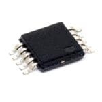
| 供应商器件封装 | 10-MSOP |
| 分辨率 | 8 bit |
| 包装 | 管件 |
| 商标 | Analog Devices |
| 安装类型 | 表面贴装 |
| 安装风格 | SMD/SMT |
| 封装 | Tube |
| 封装/外壳 | 10-TFSOP,10-MSOP(0.118",3.00mm 宽) |
| 封装/箱体 | MSOP-10 |
| 工作温度 | -40°C ~ 125°C |
| 工厂包装数量 | 50 |
| 建立时间 | 15ns |
| 接口类型 | SPI |
| 数据接口 | 串行 |
| 最大功率耗散 | 25 uW |
| 最大工作温度 | + 125 C |
| 最小工作温度 | - 40 C |
| 标准包装 | 50 |
| 电压参考 | External |
| 电压源 | 单电源 |
| 电源电压-最大 | 5.5 V |
| 电源电压-最小 | 2.5 V |
| 积分非线性 | +/- 0.25 LSB |
| 稳定时间 | 100 ns |
| 系列 | AD5425 |
| 结构 | R-2R |
| 转换器数 | 1 |
| 转换器数量 | 1 |
| 输出数和类型 | 2 电流,单极2 电流,双极 |
| 输出类型 | Current |
| 配用 | /product-detail/zh/EVAL-AD5425EBZ/EVAL-AD5425EBZ-ND/1679961 |
| 采样比 | 2.47 MSPs |
| 采样率(每秒) | 9.5M |


- 商务部:美国ITC正式对集成电路等产品启动337调查
- 曝三星4nm工艺存在良率问题 高通将骁龙8 Gen1或转产台积电
- 太阳诱电将投资9.5亿元在常州建新厂生产MLCC 预计2023年完工
- 英特尔发布欧洲新工厂建设计划 深化IDM 2.0 战略
- 台积电先进制程称霸业界 有大客户加持明年业绩稳了
- 达到5530亿美元!SIA预计今年全球半导体销售额将创下新高
- 英特尔拟将自动驾驶子公司Mobileye上市 估值或超500亿美元
- 三星加码芯片和SET,合并消费电子和移动部门,撤换高东真等 CEO
- 三星电子宣布重大人事变动 还合并消费电子和移动部门
- 海关总署:前11个月进口集成电路产品价值2.52万亿元 增长14.8%


PDF Datasheet 数据手册内容提取
8-Bit, High Bandwidth Multiplying DAC with Serial Interface Data Sheet AD5425 FEATURES GENERAL DESCRIPTION 2.5 V to 5.5 V supply operation The AD54251 is a CMOS, 8-bit, current output digital-to-analog 50 MHz serial interface converter (DAC) that operates from a 2.5 V to 5.5 V power supply, 2.47 MSPS update rate making it suitable for battery-powered applications and many INL of ±0.25 LSB other applications. 10 MHz multiplying bandwidth ±10 V reference input This DAC utilizes a double buffered, 3-wire serial interface that Low glitch energy: <2 nV-s is compatible with SPI®, QSPI™, MICROWIRE™, and most DSP Extended temperature range: −40°C to +125°C interface standards. An LDAC pin is also provided, which 10-lead MSOP package allows simultaneous updates in a multiDAC configuration. On Guaranteed monotonic power-up, the internal shift register and latches are filled with 4-quadrant multiplication 0s and the DAC outputs are 0 V. Power-on reset with brownout detection LDAC function As a result of manufacturing on a CMOS submicron process, this DAC offers excellent 4-quadrant multiplication charac- 0.4 µA typical power consumption APPLICATIONS teristics with large signal multiplying bandwidths of 10 MHz. Portable battery-powered applications The applied external reference input voltage (VREF) determines Waveform generators the full-scale output current. An integrated feedback resistor, Analog processing RFB, provides temperature tracking and full-scale voltage output Instrumentation applications when combined with an external I to V precision amplifier. Programmable amplifiers and attenuators The AD5425 is available in a small, 10-lead MSOP package. Digitally controlled calibration Programmable filters and oscillators Composite video Ultrasound Gain, offset, and voltage trimming FUNCTIONAL BLOCK DIAGRAM VDD VREF AD5425 R RFB 8-BIT IOUT1 R-2R DAC IOUT2 LDAC DAC REGISTER POWER-ON RESET INPUT LATCH SYNC CONTROL LOGIC AND SCLK INPUT SHIFT REGISTER SDIN GND 03161-001 Figure 1. 1 U.S. Patent No. 5,969,657. Rev. D Document Feedback Information furnished by Analog Devices is believed to be accurate and reliable. However, no responsibility is assumed by Analog Devices for its use, nor for any infringements of patents or other One Technology Way, P.O. Box 9106, Norwood, MA 02062-9106, U.S.A. rights of third parties that may result from its use. Specifications subject to change without notice. No license is granted by implication or otherwise under any patent or patent rights of Analog Devices. Tel: 781.329.4700 ©2004–2016 Analog Devices, Inc. All rights reserved. Trademarks and registered trademarks are the property of their respective owners. Technical Support www.analog.com
AD5425 Data Sheet TABLE OF CONTENTS Features .............................................................................................. 1 Circuit Operation ....................................................................... 14 Applications ....................................................................................... 1 Single-Supply Applications ....................................................... 15 General Description ......................................................................... 1 Adding Gain ................................................................................ 16 Functional Block Diagram .............................................................. 1 DACs Used as a Divider or Programmable Gain Element ... 16 Revision History ............................................................................... 2 Reference Selection .................................................................... 16 Specifications ..................................................................................... 3 Amplifier Selection .................................................................... 17 Timing Characteristics ..................................................................... 5 Serial Interface ............................................................................ 19 Absolute Maximum Ratings ............................................................ 6 Microprocessor Interfacing ....................................................... 19 ESD Caution .................................................................................. 6 PCB Layout and Power Supply Decoupling ................................ 22 Pin Configuration and Function Descriptions ............................. 7 Outline Dimensions ....................................................................... 23 Typical Performance Characteristics ............................................. 8 Ordering Guide .......................................................................... 23 Terminology .................................................................................... 13 Theory of Operation ...................................................................... 14 REVISION HISTORY 1/16—Rev. C to Rev. D 6/12—Rev. A to Rev. B Deleted Positive Output Voltage Section ........................................ 16 Deleted ADSP-2103 and changed ADSP-2191 to Changes to Adding Gain Section .................................................... 16 ADSP-2191M Throughout ............................................................ 19 Changes to ADSP-21xx to AD5425 Interface Section Deleted Evaluation Board Section and Operating the Evaluation and Figure 39 .................................................................................... 19 Board Section, deleted Figure 46 to Figure 49, and deleted Changes to ADSP-BF504 to ADSP-BF592 Device Family to Table 11 ............................................................................................ 23 AD5425 Interface Section, MC68HC11 Interface to AD5425 Changes to Ordering Guide .......................................................... 23 Interface Section, and Figure 40 and Figure 41 Captions ......... 20 3/05—Rev. 0 to Rev. A Changes to PIC16C6x/PIC16C7x to AD5425 Section .............. 21 Updated Format .................................................................. Universal Changes to Specifications Section ................................................... 3 9/12—Rev. B to Rev. C Added Figure 18, Figure 20, Figure 21 ........................................ 10 Change to Features ........................................................................... 1 Change to Table 7 ........................................................................... 18 2/04—Revision 0: Initial Version Rev. D | Page 2 of 24
Data Sheet AD5425 SPECIFICATIONS V = 2.5 V to 5.5 V, V = 10 V, I 2 = 0 V. Temperature range for Y version: −40°C to +125°C. All specifications T to T , unless DD REF OUT MIN MAX otherwise noted. DC performance measured with OP177, ac performance with AD8038, unless otherwise noted. Table 1. Parameter Min Typ Max Unit Test Conditions/Comments STATIC PERFORMANCE Resolution 8 Bits Relative Accuracy ±0.25 LSB Differential Nonlinearity ±0.5 LSB Guaranteed monotonic Gain Error ±10 mV Gain Error Temperature Coefficient ±5 ppm FSR/°C Output Leakage Current ±10 nA Data = 0x0000, T = 25°C, I 1 A OUT ±20 nA Data = 0x0000, T = −40°C to +125°C, I 1 OUT REFERENCE INPUT1 Reference Input Range ±10 V V Input Resistance 8 10 12 kΩ Input resistance TC = −50 ppm/°C REF R Resistance 8 10 12 kΩ Input resistance TC = −50 ppm/°C FB Input Capacitance Code Zero Scale 3 6 pF Code Full Scale 5 8 pF DIGITAL INPUT/OUTPUT1 Input High Voltage, V 1.7 V IH Input Low Voltage, V 0.6 V IL Output High Voltage, V V − 1 V V = 4.5 V to 5 V, I = 200 µA OH DD DD SOURCE V − 0.5 V V = 2.5 V to 3.6 V, I = 200 µA DD DD SOURCE Output Low Voltage, V 0.4 V V = 4.5 V to 5 V, I = 200 µA OL DD SINK 0.4 V V = 2.5 V to 3.6 V, I = 200 µA DD SINK Input Leakage Current, I 1 µA IL Input Capacitance 4 10 pF DYNAMIC PERFORMANCE1 Reference Multiplying Bandwidth 10 MHz V = ±3.5 V, DAC loaded all 1s REF Output Voltage Settling Time V = ±3.5 V, R = 100 Ω, DAC latch REF LOAD alternately loaded with 0s and 1s Measured to ±1 mV 90 160 ns Measured to ±4 mV 55 110 ns Measured to ±16 mV 50 100 ns Digital Delay 40 75 ns Interface delay time 10% to 90% Settling Time 15 30 ns Rise and fall time, V = 10 V, R = 100 Ω REF LOAD Digital-to-Analog Glitch Impulse 2 nV-s 1 LSB change around major carry V = 0 V REF Multiplying Feedthrough Error DAC latch loaded with all 0s. V = ±3.5 V REF 70 dB 1 MHz 48 dB 10 MHz Output Capacitance I 1 12 17 pF All 0s loaded OUT 25 30 pF All 1s loaded I 2 22 25 pF All 0s loaded OUT 10 12 pF All 1s loaded Digital Feedthrough 0.1 nV-s Feedthrough to DAC output with SYNC high and alternate loading of all 0s and all 1s Analog THD 81 dB V = 3.5 V p-p; all 1s loaded, f = 1 kHz REF Digital THD Clock = 1 MHz, V = 3.5 V, C = 1.8 pF REF COMP 50 kHz f 70 dB OUT 20 kHz f 73 dB OUT Rev. D | Page 3 of 24
AD5425 Data Sheet Parameter Min Typ Max Unit Test Conditions/Comments Output Noise Spectral Density 25 nV√Hz At 1 kHz SFDR Performance (Wide Band) Clock = 2 MHz , V = 3.5 V REF 50 kHz f 67 dB OUT 20 kHz f 68 dB OUT SFDR Performance (Narrow Band) Clock = 2 MHz, V = 3.5 V REF 50 kHz f 73 dB OUT 20 kHz f 75 dB OUT Intermodulation Distortion 79 dB f = 20 kHz, f = 25 kHz, clock = 2 MHz, 1 2 V = 3.5 V REF POWER REQUIREMENTS Power Supply Range 2.5 5.5 V I 0.6 µA T = 25°C, logic inputs = 0 V or V DD A DD 0.4 5 µA Logic inputs = 0 V or V , T = −40°C to +125°C DD Power Supply Sensitivity 0.001 %/% ΔV = ±5% DD 1 Guaranteed by design and characterization, not subject to production test. Rev. D | Page 4 of 24
Data Sheet AD5425 TIMING CHARACTERISTICS All input signals are specified with tr = tf = 1 ns (10% to 90% of V ) and timed from a voltage level of (V + V )/2. V =2.5 V to 5.5 V, DD IL IH DD V = 10 V, I 2 = 0 V, temperature range for Y version: −40°C to +125°C ; all specifications T to T , unless otherwise noted. REF OUT MIN MAX Table 2. Parameter1 V = 2.5 V to 5.5 V Unit Test Conditions/Comments DD f 50 MHz max Maximum clock frequency SCLK t 20 ns min SCLK cycle time 1 t 8 ns min SCLK high time 2 t 8 ns min SCLK low time 3 t 2 13 ns min SYNC falling edge to SCLK falling edge setup time 4 t 5 ns min Data setup time 5 t 3 ns min Data hold time 6 t 5 ns min SYNC rising edge to SCLK falling edge 7 t 30 ns min Minimum SYNC high time 8 t 0 ns min SCLK falling edge to LDAC falling edge 9 t 12 ns min LDAC pulse width 10 t 10 ns min SCLK falling edge to LDAC rising edge 11 1 Guaranteed by design and characterization, not subject to production test. 2 Falling or rising edge as determined by control bits of serial word. t1 SCLK t2 t3 t8 t4 t7 SYNC t6 t5 DIN DB7 DB0 t10 t9 LDAC1 t11 LDAC2 N12ASOYSTNYENCSCH:HRROONNOOUUS SL DLDAACC U UPDPDAATET EM MOODDE.E. 03161-002 Figure 2. Timing Diagram Rev. D | Page 5 of 24
AD5425 Data Sheet ABSOLUTE MAXIMUM RATINGS T = 25°C, unless otherwise noted. A Stresses at or above those listed under Absolute Maximum Ratings may cause permanent damage to the product. This is a Table 3. stress rating only; functional operation of the product at these Parameter Rating or any other conditions above those indicated in the operational V to GND −0.3 V to +7 V DD section of this specification is not implied. Operation beyond V , R to GND −12 V to +12 V REF FB the maximum operating conditions for extended periods may I 1, I 2 to GND −0.3 V to V + 0.3 V OUT OUT DD affect product reliability. Logic Input and Output1 −0.3 V to V + 0.3 V DD Operating Temperature Range ESD CAUTION Extended Industrial (Y Version) −40°C to +125°C Storage Temperature Range −65°C to +150°C Junction Temperature 150°C 10-lead MSOP 206°C/W θ Thermal Impedance JA Lead Temperature, Soldering 300°C (10 secs) IR Reflow, Peak Temperature 235°C (<20 secs) 1 Overvoltages at SCLK, SYNC, DIN, and LDAC are clamped by internal diodes. Current must be limited to the maximum ratings given. Rev. D | Page 6 of 24
Data Sheet AD5425 PIN CONFIGURATION AND FUNCTION DESCRIPTIONS IOUT1 1 10 RFB IOUT2 2 AD5425 9 VREF GND 3 TOP VIEW 8 VDD SSCDLIKN 45 (Not to Scale) 76 LSDYANCC 03161-003 Figure 3. Pin Configuration Table 4. Pin Function Descriptions Pin No. Mnemonic Function 1 I 1 DAC Current Output. OUT 2 I 2 DAC Analog Ground. This pin must normally be tied to the analog ground of the system. OUT 3 GND Digital Ground Pin. 4 SCLK Serial Clock Input. Data is clocked into the input shift register on each falling edge of the serial clock input. This device can accommodate clock rates of up to 50 MHz. 5 SDIN Serial Data Input. Data is clocked into the 8-bit input register on each falling edge of the serial clock input. 6 SYNC Active Low Control Input. This is the frame synchronization signal for the input data. When SYNC goes low, it powers on the SCLK and DIN buffers and the input shift register is enabled. Data is transferred on each falling edge of the following 8 clocks. 7 LDAC Load DAC Input. Updates the DAC output. The DAC is updated when this signal goes low or alternatively; if this line is held permanently low, an automatic update mode is selected whereby the DAC is updated after 8 SCLK falling edges with SYNC low. 8 V Positive Power Supply Input. This device can be operated from a supply of 2.5 V to 5.5 V. DD 9 V DAC Reference Voltage Input Terminal. REF 10 R DAC Feedback Resistor Pin. Establishes voltage output for the DAC by connecting to external amplifier output. FB Rev. D | Page 7 of 24
AD5425 Data Sheet TYPICAL PERFORMANCE CHARACTERISTICS 0.20 0.4 TA = 25°C TA = 25°C VREF = 10V VDD = 5V 0.15 VDD = 5V 0.2 0.10 MIN DNL 0.05 0 B) SB) NL (LS 0 DNL (L –0.2 I–0.05 MAX DNL –0.10 –0.4 –0.15 –0.200 50 100 CODE150 200 250 03161-004 –0.62 3 4 REF5ERENC6E VOLTA7GE 8 9 10 03161-007 Figure 4. Integral Nonlinearity (INL) vs. Code (8-Bit DAC) Figure 7. DNL vs. Reference Voltage 0.20 1.6 TA = 25°C VREF = 10V 0.15 VDD = 5V 1.4 0.10 1.2 0.05 nA) 1.0 IOUT1 VDD 5V B) GE ( INL (LS–0.005 LEAKAT 00..86 U O I –0.10 0.4 IOUT1 VDD 3V –0.15 0.2 –0.200 50 100 CODE150 200 250 03161-005 0–40 –20 0 T2E0MPER4A0TURE6 (0°C) 80 100 120 03161-008 Figure 5. Differential Nonlinearity (DNL) vs. Code (8-Bit DAC) Figure 8. IOUT1 Leakage Current vs. Temperature 0.3 TA = 25°C 5 VREF = 10V VDD = 5V 4 0.2 3 MAX INL VDD = 5V 2 0.1 V) 1 B) m INL (LS 0 ERROR ( –01 VDD = 2.5V –0.1 MIN INL –2 –3 –0.2 –4 –0.32 3 4 REF5ERENC6E VOLTA7GE 8 9 10 03161-006 –5–60 –40 –20 0 TE2M0PERA40TURE6 0(°C) 80 100 120 140 03161-009 Figure 9. Gain Error vs. Temperature Figure 6. INL vs. Reference Voltage Rev. D | Page 8 of 24
Data Sheet AD5425 0.5 2.5 TA = 25°C VDD = 5V VDD = 3V VREF = 0V VREF = 0V 2.0 0.3 GAIN ERROR 0.1 MAX INL MAX DNL V) 1.5 m Bs GE ( 1.0 LS –0.1 LTA O MIN DNL V 0.5 MIN INL OFFSET ERROR –0.3 0 –0.50.5 0.6 0.7 0.8 0.9VBI1A.S0 (V)1.1 1.2 1.3 1.4 1.5 03161-010 –0.50.5 1.0 VBI1A.S5 (V) 2.0 2.5 03161-013 Figure 10. Linearity vs. VBIAS Voltage Applied to IOUT2 Figure 13. Gain and Offset Errors vs. Voltage Applied to IOUT2 1.4 10.0 TA = 25°C TA = 25°C 1.2 VDD = 3V VDD = 5V VREF = 0V 8.0 VREF = 2.5V 1.0 6.0 0.8 V) GAIN ERROR V) E(m 0.6 E (m 4.0 G G OLTA 0.4 OFFSET ERROR OLTA 2.0 OFFSET ERROR V 0.2 V 0 0 –2.0 –0.2 GAIN ERROR –0.40.5 VBI1A.S0 (V) 1.5 03161-011 –4.00 0.5 1.0VBIAS (V)1.5 2.0 2.5 03161-014 Figure 11. Gain and Offset Errors vs. VBIAS Voltage Applied to IOUT2 Figure 14. Gain and Offset Errors vs. VBIAS Voltage Applied to IOUT2 0.5 1.0 VDD = 5V TA = 25°C VREF = 0V 0.8 VDD = 5V VREF = 2.5V 0.3 0.6 MIN INL BIAS 0.4 MAX INL MAX DNL MAX INL BIAS 0.1 0.2 Bs Bs 0 S S L L –0.1 –0.2 MAX DNL BIAS MIN DNL MIN INL –0.4 MIN DNL BIAS –0.3 –0.6 –0.8 –0.50.5 1.0 VBI1A.S5 (V) 2.0 2.5 03161-012 –1.00 0.5 VBI1A.S0 (V) 1.5 2.0 03161-015 Figure 12. Linearity vs. VBIAS Voltage Applied to IOUT2 Figure 15. Linearity vs. VBIAS Voltage Applied to IOUT2 Rev. D | Page 9 of 24
AD5425 Data Sheet 0.7 0.060 0.6 TA = 25°C 0.050 VN07DRxDGF 5 F=V T2, O.00V 40 9xRn8EV0F0s TVAARD E8=F0 23=58 °0 CAVMPLIFIER CCOMP = 1.8pF 0.040 0.5 mA) 0.4 VDD = 5V AGE (V)0.030 VN0xDR8DG0 3 0=V T 0, O.00 V08 x8R7nEFVFFs NT ( OLT0.020 CURRE 0.3 TPUT V0.010 VN0xDR7DGF 3 F=V T1, O.08V 70 7xRn8EV0F0s 0.2 OU 0 VDD = 2.5V 0.1 –0.010 VDD 5V, 0V REF VDD = 3V NRG = 0.119nVs, 0x800 TO 0x7FF 00 1 INP2UT VOLTAGE3 (V) 4 5 03161-016 –0.0200 50 100 TIM1E5 0(ns) 200 250 300 03161-019 Figure 16. Supply Current vs. Input Voltage Figure 19. Midscale Transition, VREF = 3.5 V 11..86 TA = 25°C ––12606 TLZAOS A=T DO2I5 NF°GSC ADDLBBL11 10ON GE (V) 11..42 VIH ––––12338406 DDDDBBBB9876 OLD VOLTA 10..08 VIL GAIN (dB) ––––44562840 DDDDBBBB5432 RESH 0.6 ––6762 DDBB10 TA = 25°C TH 0.4 –78 VDD = 5V –84 VREF =±3.5V 0.2 ––9906 ALL OFF CCOMP =I N1.P8UpTF AD8083 AMPLIFIER 02.5 3.0 3.5 VOLT4A.0GE (V) 4.5 5.0 5.5 03161-017 –1021 10 100 1FkREQU1E0NkCY (1H0z0)k 1M 10M 100M 03161-020 Figure 17. Threshold Voltages vs. Supply Voltage Figure 20. Reference Multiplying Bandwidth vs. Frequency and Code 0.2 3 VREF =±0.15V, AD8038 CC 1pF VREF =±2V, AD8038 CC 1pF 0 0 VREF =±3.51V, AD8038 CC 1.8pF B) –0.2 B) VREF =±2V, AD8038 CC 1.47pF AIN (d AIN (d –3 VREF =±0.15V, AD8038 CC 1.47pF G –0.4 G –6 –0.6 TA = 25°C VDD = 5V VREF =±3.5V TA = 25°C CCOMP = 1.8pF VDD = 5V AD8083 AMPLIFIER AD8038 AMPLIFIER –0.81 10 100 1FkREQU1E0NkCY (1H0z0)k 1M 10M 100M 03161-018 –910k 100k FREQUE1MNCY (Hz) 10M 100M 03161-021 Figure 18. Reference Multiplying Bandwidth—All 1s Loaded Figure 21. Reference Multiplying Bandwidth vs. Frequency and Compensation Capacitor Rev. D | Page 10 of 24
Data Sheet AD5425 –60 0 TA = 25°C TA = 25°C VDD = 3V –10 VDD = 5V –65 VREF = 3.5V p-p –20 VARDE8F0 3=8 3 A.5MVPLIFIER –30 –70 –40 dB) B) –50 D + N ( –75 FDR (d –60 TH S –70 –80 –80 –85 –90 –100 –901 10 100FREQUE1NkCY (Hz)10k 100k 1M 03161-022 –1100 200k F4R00EkQUENCY6 (0H0zk) 800k 1M 03161-025 Figure 22. THD and Noise vs. Frequency Figure 25. Wideband SFDR, Clock = 2 MHz, fOUT = 20 kHz 20 0 VDD = 3V TA = 25°C AMPLIFIER = AD8038 –10 VDD = 5V 0 VREF = 3.5V –20 AD8038 AMPLIFIER N TIO –20 –30 C E –40 J RE –40 B) –50 SUPPLY –60 FULL SCALE SFDR (d ––6700 R WE –80 ZERO SCALE –80 O P –90 –100 –100 –1201 10 100 FRE1QkUENC1Y0 (kHz) 100k 1M 10M 03161-023 –11010k 12k 14k 16k F1R8EkQU2E0NkCY 2(H2kz) 24k 26k 28k 30k 03161-026 Figure 23. Power Supply Rejection vs. Frequency Figure 26. Narrow-Band SFDR, Clock = 2 MHz, fOUT = 20 kHz 0 0 TA = 25°C TA = 25°C –10 VDD = 5V –10 VDD = 5V VREF = 3.5V VREF = 3.5V –20 AD8038 AMPLIFIER –20 AD8038 AMPLIFIER –30 –30 –40 –40 B) –50 B) –50 d d DR ( –60 DR ( –60 F F S –70 S –70 –80 –80 –90 –90 –100 –100 –1100 200k F4R00EkQUENCY6 (0H0zk) 800k 1M 03161-024 –11025k 30k 35k 40k F4R5EkQU5E0NkCY 5(H5kz) 60k 65k 70k 75k 03161-027 Figure 24. Wideband SFDR, Clock = 2 MHz, fOUT = 50 kHz Figure 27. Narrow-Band SFDR, Clock = 2 MHz, fOUT = 50 kHz Rev. D | Page 11 of 24
AD5425 Data Sheet 0 VDD = 5V –10 VREF = 3.5V AD8038 AMPLIFIER –20 –30 –40 B) d –50 D ( M I –60 –70 –80 –90 –10010k 15k F2R0EkQUENCY 2(H5kz) 30k 35k 03161-028 Figure 28. Narrow-Band IMD (±50%) Clock = 2 MHz, fOUT1 = 20 kHz, fOUT2 = 25 kHz Rev. D | Page 12 of 24
Data Sheet AD5425 TERMINOLOGY Relative Accuracy Digital Feedthrough Relative accuracy or endpoint nonlinearity is a measure of the When the device is not selected, high frequency logic activity on maximum deviation from a straight line passing through the the device digital inputs can be capacitively coupled to display endpoints of the DAC transfer function. It is measured after as noise on the I pins and subsequently into the following OUT adjusting for zero and full scale and is normally expressed in circuitry. This noise is digital feedthrough. LSBs or as a percentage of full-scale reading. Multiplying Feedthrough Error Differential Nonlinearity This is the error due to capacitive feedthrough from the DAC Differential nonlinearity is the difference between the measured reference input to the DAC I 1 terminal, when all 0s are OUT change and the ideal 1 LSB change between any two adjacent loaded to the DAC. codes. A specified differential nonlinearity of −1 LSB maximum Total Harmonic Distortion (THD) over the operating temperature range ensures monotonicity. The DAC is driven by an ac reference. The ratio of the rms sum Gain Error of the harmonics of the DAC output to the fundamental value is Gain error or full-scale error is a measure of the output error the THD. Usually only the lower order harmonics are included, between an ideal DAC and the actual device output. For these such as second to fifth. DACs, ideal maximum output is V − 1 LSB. Gain error of the REF ( ) V2+V2+V 2+V2 DACs is adjustable to 0 with external resistance. THD=20log 2 3 4 5 V Output Leakage Current 1 Output leakage current is current that flows in the DAC ladder Digital Intermodulation Distortion (IMD) switches when the switches are turned off. The I 1 terminal OUT Second-order IMD measurements are the relative magnitude of can be measured by loading all 0s to the DAC and measuring the fa and fb tones generated digitally by the DAC and the the I 1 current. Minimum current flows in the I 2 line OUT OUT second-order products at 2fa − fb and 2fb − fa. when the DAC is loaded with all 1s. Spurious-Free Dynamic Range (SFDR) Output Capacitance SFDR is the usable dynamic range of a DAC before spurious Capacitance from I 1 or I 2 to AGND. OUT OUT noise interferes or distorts the fundamental signal. It is the mea- Output Current Settling Time sure of the difference in amplitude between the fundamental This is the amount of time it takes for the output to settle to a and the largest harmonically or nonharmonically related spur specified level for a full-scale input change. For these devices, it from dc to full Nyquist bandwidth (half the DAC sampling rate, is specified with a 100 Ω resistor to ground. or fS/2). Narrow-band SFDR is a measure of SFDR over an arbitrary window size, in this case 50% of the fundamental. The settling time specification includes the digital delay from Digital SFDR is a measure of the usable dynamic range of the SYNC rising edge to the full-scale output charge. DAC when the signal is a digitally generated sine wave. Digital-to-Analog Glitch Impulse The amount of charge injected from the digital inputs to the analog output when the inputs change state. This is normally specified as the area of the glitch in either pA-s or nV-s depending upon whether the glitch is measured as a current or voltage signal. Rev. D | Page 13 of 24
AD5425 Data Sheet THEORY OF OPERATION The AD5425 is an 8-bit current output DAC consisting of a With a fixed 10 V reference, the circuit shown in Figure 30 gives standard inverting R-2R ladder configuration. A simplified a unipolar 0 V to −10 V output voltage swing. When V is an ac IN diagram is shown in Figure 29. The feedback resistor, R , has a signal, the circuit performs 2-quadrant multiplication. FB value of R. The value of R is typically 10 kΩ (minimum 8 kΩ Table 5 shows the relationship between digital code and the and maximum 12 kΩ). If I 1 and I 2 are kept at the same OUT OUT expected output voltage for unipolar operation. potential, a constant current flows in each ladder leg, regardless of digital input code. Therefore, the input resistance presented Table 5. Unipolar Code Table at V is always constant and nominally of value R. The DAC Digital Input Analog Output (V) REF output, IOUT, is code dependent, producing various resistances 1111 1111 −VREF (255/256) and capacitances. When choosing the external amplifier, take 1000 0000 −V (128/256) = −V /2 REF REF into account the variation in impedance generated by the DAC 0000 0001 −V (1/256) REF on the amplifiers inverting input node. 0000 0000 −V (0/256) = 0 REF R R R VREF VDD R2 2R 2R 2R 2R 2R S1 S2 S3 S8 R C1 RFB VDD RFB DACA N DDA DTAR ILVAETRCSHES IIOOUUTT12 03161-029 VREF R1 SVYRNECFSCLAKDS5D4I2N5GNDIIOOUUTT21 AA11 VTOOU–TV =R E0F Figure 29. Simplified Ladder Access is provided to the V , R , I 1, and I 2 terminals of MICROCONTROLLER AGND REF FB OUT OUT the DAC, making the device extremely versatile and allowing it NOTES: ttoo bper ocvoindfeig au ruendi pino lsaerv eoruatlp duitff, ebriepnot loapr eoruattipnugt ,m oor dines ,s ifnorg leex-asmuppplely, 12..RCIF11 A AP1HN IADSS ARE 2H CUIGOSHME DPSE PONENSELADYT AIIFOM NGP AL(1IIFNpIF EA RTDO.J U2SpFT)M MEANYT BISE R REEQQUUIRIREEDD. 03161-030 modes of operation in unipolar mode or 4-quadrant multiplication Figure 30. Unipolar Operation in bipolar mode. Note that a matching switch is used in series with R3 the internal R feedback resistor. If users attempt to measure 20kΩ FB R , power must be applied to V to achieve continuity. R5 FB DD VDD R2 20kΩ CIRCUIT OPERATION Unipolar Mode C1 VDD RFB R4 Ucosninfigg ua rseidn gtloe porpoevriadteio 2n-aqlu aamdrpalnifti emr, uthltiisp ldyeinvigc eo pcaenra etiaosnil yo rb ea V±R1E0VF R1 VREF AD5425 IIOOUUTT12 AA11 10kΩ A2 unipolar output voltage swing, as shown in Figure 30. SYNCSCLK SDIN GND VOUT =–VREF TO +VREF When an output amplifier is connected in unipolar mode, the MICROCONTROLLER AGND output voltage is given by NOTES: D V =−V × 1.R1 AND R2 ARE USED ONLY IF GAIN ADJUSTMENT IS REQUIRED. ADJUST R1 FOR OUT REF 2n VOUT = 0 V WITH CODE 10000000 LOADED TO DAC. wtoh tehree DDA isC th, ien f rtahcitsi ocnasael r0e ptore 2se5n5t,a atinodn no fi sth teh ed inguitmal bweorr odf l obaitdse. d 23..MCSP1A ETPECHDHA ISANEMG PC ALONIMFDIPE TERRN.ASCAKTIINOGN I(S1 pEFS TSOE N2TpIFA)L M FAOYR B REE RSEISQTUOIRRE PDA IIFR SA 1R/3A 2A NISD A R H4I.GH 03161-031 Figure 31. Bipolar Operation (4-Quadrant Multiplication) Note that the output voltage polarity is opposite to the V REF polarity for dc reference voltages. This DAC is designed to operate with either negative or positive reference voltages. The VDD power pin is used by only the internal digital logic to drive the on and off states of the DAC switches. This DAC is also designed to accommodate ac reference input signals in the range of −10 V to +10 V. Rev. D | Page 14 of 24
Data Sheet AD5425 Bipolar Operation As D varies from 0 to 255, the output voltage varies from In some applications, it may be necessary to generate full V = V to V = 2V − V OUT BIAS OUT BIAS IN 4-quadrant multiplying operation or a bipolar output swing. VDD This can be easily accomplished by using another external amplifier and some external resistors, as shown in Figure 31. In C1 VDD RFB this circuit, the second amplifier, A2, provides a gain of 2. Biasing IOUT1 the external amplifier with an offset from the reference voltage, VIN VREF AA11 VOUT results in full 4-quadrant multiplying operation. The transfer IOUT2 GND function of this circuit shows that both negative and positive output voltages are created as the input data, D, is incremented from code zero (V = −V ), to midscale (V = 0 V ), to full OUT REF OUT scale (V = +V ). OUT REF V =(V × D/2n−1)−V VBIAS OUT REF REF NOTES: Wloahdeerde tDo itsh teh De AfrCac atinodn anl irse tphree sreensotalutitoinon o fo ft hthe ed DigAitaCl .w ord 12..ACRD1E QDPIUHTIAIROSENEDA CLIFO P AMIN1P SEIS NO ASM AHITTIGTIOEHND S (FP1OpERFE DTC OLA AM2RpPFILT)IY FM.IEARY. BE 03161-032 When V is an ac signal, the circuit performs 4-quadrant Figure 32. Single-Supply Current Mode Operation IN multiplication. V must be a low impedance source capable of sinking and BIAS Table 6 shows the relationship between digital code and the sourcing all possible variations in current at the I 2 terminal OUT expected output voltage for bipolar operation. without any problems. It is important to note that V is limited to low voltages because Table 6. Bipolar Code Table IN the switches in the DAC ladder no longer have the same source- Digital Input Analog Output (V) drain drive voltage. As a result, the on resistance differs and this 1111 1111 +V (127/128) REF degrades the linearity of the DAC. 1000 0000 0 0000 0001 −V (127/128) Voltage Switching Mode of Operation REF 0000 0000 −VREF (128/128) Figure 33 shows this DAC operating in the voltage switching mode. The reference voltage V is applied to the I 1 pin, I 2 is IN OUT OUT Stability connected to AGND, and the output voltage is available at the V REF In the I to V configuration, the I of the DAC and the terminal. In this configuration, a positive reference voltage results OUT inverting node of the operational amplifier must be connected in a positive output voltage, making single-supply operation as closely as possible and proper printed circuit board (PCB) possible. The output from the DAC is voltage at a constant layout techniques must be employed. Since every code change impedance (the DAC ladder resistance), thus an operational corresponds to a step function, gain peaking can occur if the amplifier is necessary to buffer the output voltage. The operational amplifier has limited gain bandwidth product (GBP) reference input no longer sees constant input impedance, but and there is excessive parasitic capacitance at the inverting node. one that varies with code. So, the voltage input must be driven This parasitic capacitance introduces a pole into the open-loop from a low impedance source. response, which can cause ringing or instability in closed-loop VDD R1 R2 applications. An optional compensation capacitor, C1, can be added in parallel RFB VDD with RFB for stability, as shown in Figure 30 and Figure 31. Too VIN IOUT1 AA11 VOUT VREF small a value of C1 can produce ringing at the output, while too IOUT2 large a value can adversely affect the settling time. C1 must be GND found empirically, but 1 pF to 2 pF is generally adequate for compensation. NOTES: SCuINrrGenLtE M-SoUdPeP OLpYe rAaPtiPonL ICATIONS 12..ACIFD1 A DP1IHT IASIOS ANE AH CLIGO PHMIN PSSEP NOESEMADITT ATIOMENDP L(F1IOFpIRFE RTCO.L A2RpFIT)Y M.AY BE REQUIRED 03161-033 In the current mode circuit of Figure 32, I 2 and hence I 1 Figure 33. Single-Supply Voltage Switching Mode Operation OUT OUT is biased positive by an amount applied to V . In this config- BIAS uration, the output voltage is given by V = [D × (R /R ) × (V − V )] + V OUT FB DAC BIAS IN BIAS Rev. D | Page 15 of 24
AD5425 Data Sheet It is important to note that V is limited to low voltage because However, if the DAC has a linearity specification of ±0.5 LSB, IN the switches in the DAC ladder no longer have the same source then D can in fact have a weight anywhere in the range 15.5/256 to drain drive voltage. As a result, the on resistance differs, which 16.5/256. Therefore, the possible output voltage is in the range degrades the linearity of the DAC. of 15.5 V to 16.5 V —an error of 3%, even though the DAC IN IN itself has a maximum error of 0.2%. V must also not go negative by more than 0.3 V, otherwise an IN internal diode turns on, exceeding the maximum ratings of the VDD VIN device. In this type of application, the full range of the DAC multiplying capability is lost. RFB VDD ADDING GAIN IOUT1 VREF In applications where the output voltage is required to be GND greater than V , gain can be added with an additional external IN amplifier or it can be achieved in a single stage. It is important to take into consideration the effect of temperature coefficients of the thin film resistors of the DAC. Simply placing a resistor in VOUT series with the R resistor causes mismatches in the temp- FB ecoraetfufircei ecnote fefrircoierns.t sIn asnteda rde,s tuhlets c iinrc luaritg oerf Fgaiginu rtee m34p iesr aat urerceo m- N1.OATDED:ITIONAL PINS OMITTED FOR CLARITY. 03161-036 mended method of increasing the gain of the circuit. R1, R2, Figure 35. Current Steering DAC Used as a Divider or Programmable Gain Element and R3 must all have similar temperature coefficients but do not need to match the temperature coefficients of the DAC. This DAC leakage current is also a potential error source in divider approach is recommended in circuits where gains of greater circuits. The leakage current must be counterbalanced by an than 1 are required. Note that R R2//R3 and a gain error opposite current supplied from the operational amplifier FB percentage of 100 × (R2//R3)/R must be taken into consideration. through the DAC. Since only a fraction, D, of the current into FB ≫ the V terminal is routed to the I 1 terminal, the output VDD REF OUT voltage has to change as follows: C1 Output Error Voltage Due to DAC Leakage = (Leakage × R)/D VDD RFB R1 IOUT1 where R is the DAC resistance at the V terminal. For a DAC VIN VREF A1 VOUT REF IOUT2 R3 leakage current of 10 nA, R = 10 kΩ. With a gain (that is, 1/D) GND of 16, the error voltage is 1.6 mV. GAIN = R2 + R3 R2 R2 REFERENCE SELECTION R1 = R2R3 NOTES: R2 + R3 When selecting a reference for use with the AD5425 current 12..ACIFD1 A DP1IHT IASIOS ANE AH CLIGO PHMIN PSSEP NOESEMADITT ATIOMENDP L(F1IOFpIRFE RTCO.L A2RpFIT)Y M.AY BE REQUIRED 03161-035 oteumtppuetr aDtuArCe ,c poaeyf faicttieenntti sopne tcoif itchaet iroenfe. rTenhcise poaurtapmute tveorl tnaogte only affects the full-scale error, but can also affect the linearity (INL Figure 34. Increasing the Gain of Current Output DAC and DNL) performance. The reference temperature coefficient DACs USED AS A DIVIDER OR PROGRAMMABLE must be consistent with the system accuracy specifications. For GAIN ELEMENT example, an 8-bit system required to hold the overall specification Current steering DACs are very flexible and lend themselves to to within 1 LSB over the temperature range 0°C to 50°C dictates many different applications. If this type of DAC is connected as that the maximum system drift with temperature must be less the feedback element of an operational amplifier and R is used than 78 ppm/°C. A 12-bit system with the same temperature FB as the input resistor as shown in Figure 35, then the output range to overall specification within 2 LSB requires a maximum voltage is inversely proportional to the digital input fraction, D. drift of 10 ppm/°C. By choosing a precision reference with a low output temperature coefficient, this error source can be minimized. For D = 1 − 2−n, the output voltage is Table 7 suggests some of the references available from Analog VOUT = −VIN/D = −VIN/(1 − 2−n) Devices, Inc., that are suitable for use with this range of current As D is reduced, the output voltage increases. For small values of D, output DACs. it is important to ensure that the amplifier does not saturate and that the required accuracy is met. For example, an 8-bit DAC driven with the Binary Code 0x10 (00010000), that is, 16 decimal, in the circuit of Figure 35, causes the output voltage to be 16 × V . IN Rev. D | Page 16 of 24
Data Sheet AD5425 AMPLIFIER SELECTION Common-mode rejection of the operational amplifier is important in voltage switching circuits, since it produces a code The primary requirement for the current steering mode is an dependent error at the voltage output of the circuit. Most amplifier with low input bias currents and low input offset vol- operational amplifiers have adequate common-mode rejection tage. The input offset voltage of an operational amplifier is for use at an 8-bit resolution. multiplied by the variable gain (due to the code dependent output resistance of the DAC) of the circuit. Provided the DAC switches are driven from true wideband low impedance sources (V and AGND), they settle quickly. Conse- A change in this noise gain between two adjacent digital IN quently, the slew rate and settling time of a voltage switching fractions produces a step change in the output voltage due to DAC circuit is determined largely by the output operational the amplifier input offset voltage. This output voltage change is amplifier. To obtain minimum settling time in this configuration, superimposed on the desired change in output between the two it is important to minimize capacitance at the V node codes and gives rise to a differential linearity error, which if REF (voltage output node in this application) of the DAC. This is large enough, could cause the DAC to be nonmonotonic. done by using low inputs capacitance buffer amplifiers and The input bias current of an operational amplifier also generates careful board design. an offset at the voltage output as a result of the bias current Most single-supply circuits include ground as part of the analog flowing in the feedback resistor, R . Most operational FB signal range, which requires an amplifier that can handle rail-to-rail amplifiers have input bias currents low enough to prevent any signals. There is a large range of single-supply amplifiers available significant errors. from Analog Devices. Table 7. Suitable Analog Devices Precision References Part No. Output Voltage (V) Initial Tolerance (%) Temp Drift (ppm/°C) I (mA) Output Noise (µV p-p) Package SS ADR01 10 0.05 3 1 20 SOIC-8 ADR01 10 0.05 9 1 20 TSOT-23, SC70 ADR02 5 0.06 3 1 10 SOIC-8 ADR02 5 0.06 9 1 10 TSOT-23, SC70 ADR03 2.5 0.10 3 1 6 SOIC-8 ADR03 2.5 0.10 9 1 6 TSOT-23, SC70 ADR06 3 0.10 3 1 10 SOIC-8 ADR06 3 0.10 9 1 10 TSOT-23, SC70 ADR431 2.5 0.04 3 0.8 3.5 SOIC-8 ADR435 5 0.04 3 0.8 8 SOIC-8 ADR391 2.5 0.16 9 0.12 5 TSOT-23 ADR395 5 0.10 9 0.12 8 TSOT-23 Rev. D | Page 17 of 24
AD5425 Data Sheet Table 8. Suitable Precision Analog Devices Operational Amplifiers 0.1 Hz to 10 Hz Part No. Supply Voltage (V) V (Max) (µV) I (Max) (nA) Noise (µV p-p) Supply Current (µA) Package OS B OP97 ±2 to ±20 25 0.1 0.5 600 SOIC-8 OP1177 ±2.5 to ±15 60 2 0.4 500 MSOP, SOIC-8 AD8551 2.7 to 5 5 0.05 1 975 MSOP, SOIC-8 AD8603 1.8 to 6 50 0.001 2.3 50 TSOT AD8628 2.7 to 6 5 0.1 0.5 850 TSOT, SOIC-8 Table 9. Suitable High Speed Analog Devices Operational Amplifiers Part No. Supply Voltage (V) BW at ACL (MHz) Slew Rate (V/µs) V (Max) (µV) I (Max) (nA) Package OS B AD8065 5 to 24 145 180 1500 6000 SOIC-8, SOT-23,MSOP AD8021 ±2.5 to ±12 490 120 1000 10500 SOIC-8, MSOP AD8038 3 to 12 350 425 3000 750 SOIC-8, SC70-5 AD9631 ±3 to ±6 320 1300 10000 7000 SOIC-8 Rev. D | Page 18 of 24
Data Sheet AD5425 SERIAL INTERFACE ADSP-2191M1 AD54251 The AD5425 has a simple 3-wire interface that is compatible SPIxSEL SYNC with SPI, QSPI, MICROWIRE, and DSP interface standards. MOSI SDIN Data is written to the device in 8-bit words. This 8-bit word consists of 8 data bits, as shown in Figure 36. SCK SCLK DB7 (MSB) DB0 (LSB) DB7 DB6 DB5 DDABT4A BDIBT3S DB2 DB1 DB0 03161-037 1ADDITIONAL PFIiNgSu rOeM 3I7T.T AEDDS FPO-2R1 C9L1AMR ISTPYI. to AD5425 Interface 03161-038 Figure 36. 8-Bit Input Shift Register Contents A serial interface between the DAC and DSP SPORT is shown SYNC is an edge triggered input that acts as a frame synchro- in Figure 38. In this interface example, SPORT0 is transfers data nization signal and chip enable. Data can be transferred into the to the DAC shift register. Transmission is initiated by writing a device only while SYNC is low. To start the serial data transfer, word to the Tx register after the SPORT has been enabled. In a SYNC must be taken low, observing the minimum SYNC falling write sequence, data is clocked out on each rising edge of the to SCLK falling edge setup time, t4. DSP serial clock and clocked into the DAC input shift register on the falling edge of the SCLK. The update of the DAC output After loading eight data bits to the shift register, the SYNC line takes place on the rising edge of the SYNC signal. is brought high. The contents of the DAC register and the output are updated by bringing LDAC low any time after the 8-bit data ADSP-2191M1 AD54251 transfer is complete, as seen in the timing diagram of Figure 2. TFS SYNC LDAC can be tied permanently low if required. For another serial transfer to take place, the interface must be enabled by DT SDIN another falling edge of SYNC. SCLK SCLK Low Power Serial Interface Tfuol lmy pinoiwmeirzse uthpe o pnolyw werh ceonn tshuem dpetviiocne iosf btheien dge wvircitet,e tnh eto i,n tthearfta icse, 1ADDITIONAL PINS OMITTED FOR CLARITY. 03161-039 Figure 38. ADSP-2191M SPORT to AD5425 Interface on the falling edge of SYNC. The SCLK and SDIN input buffers are powered down on the rising edge of SYNC. Communication between two devices at a given clock speed is possible when the following specifications from one device to the MICROPROCESSOR INTERFACING other are compatible: frame sync delay and frame sync setup and Microprocessor interfacing to this DAC is via a serial bus that hold, data delay and data setup and hold, and SCLK width. The uses standard protocol compatible with microcontrollers and DAC interface expects a t4 (SYNC falling edge to SCLK falling DSP processors. The communications channel is a 3-wire inter- edge setup time) of 13 ns minimum. Consult the ADSP-21xx face consisting of a clock signal, a data signal, and a synchro- user manual for information on clock and frame sync frequencies nization signal. An LDAC pin is also included. The AD5425 for the SPORT register. requires an 8-bit word with the default being data valid on the Table 10. SPORT Control Register Setup falling edge of SCLK, but this is changeable via the control bits Name Setting Description in the data-word. TFSW 1 Alternate framing ADSP-21xx to AD5425 Interface INVTFS 1 Active low frame signal The ADSP-21xx family of DSPs is easily interfaced to this family of DTYPE 00 Right justify data DACs without extra glue logic. Figure 37 shows an example of ISCLK 1 Internal serial clock an SPI interface between the DAC and the ADSP-2191M. SCK TFSR 1 Frame every word of the DSP drives the serial clock line, SCLK. SYNC is driven ITFS 1 Internal framing signal from one of the port lines, in this case SPIxSEL. SLEN 0111 8-bit data-word Rev. D | Page 19 of 24
AD5425 Data Sheet ADSP-BF504 to ADSP-BF592 Device Family to AD5425 Data on RxD is clocked out of the microcontroller on the rising Interface edge of TxD and is valid on the falling edge. As a result, no glue The ADSP-BF504 to ADSP-BF592 device family of processors logic is required between the DAC and microcontroller interface. has an SPI-compatible port that enables the processor to comm- P3.3 is taken high at the completion of this cycle. The 8051 unicate with SPI-compatible devices. A serial interface between provides the LSB of the SBUF register as the first bit in the data the ADSP-BF504 to ADSP-BF592 device family and the AD5425 stream. The DAC input register requires that the MSB is the DAC is shown in Figure 39. In this configuration, data is trans- first bit received. The transmit routine must take this into ferred through the MOSI (master output/slave input) pin. SYNC account. is driven by the SPI chip select pin, which is a reconfigured 80511 AD54251 programmable flag pin. TxD SCLK ADSP-BF5xx1 AD54251 RxD SDIN SPIxSEL SYNC P1.1 SYNC MOSI SDIN SCK SCLK 1ADDITIONAL PINS OMITTED FOR CLARITY. 03161-042 1ADDITIONAL PINS OMITTED FOR CLARITY. 03161-040 MC68HC11 IFnigtuerref 4a1c. e80 tCo5 1A/8D05L5412 to5 A IDn5t4e2r5f aIncteer face Figure 39. ADSP-BF504 to ADSP-BF592 Device Family to AD5425 Interface Figure 42 shows an example of a serial interface between the (ADSP-BFxx Denotes the ADSP-BF504 to ADSP-BF592) DAC and the MC68HC11 microcontroller. The serial peripheral The ADSP-BF504 to ADSP-BF592 processors incorporate interface (SPI) on the MC68HC11 is configured for master mode channel synchronous serial ports (SPORT). A serial interface (MSTR = 1), clock polarity bit (CPOL) = 0, and the clock phase between the DAC and the DSP SPORT is shown in Figure 40. bit (CPHA) = 1. The SPI is configured by writing to the SPI control When the SPORT is enabled, initiate transmission by writing a register (SPCR). SCK of the MC68HC11 drives the SCLK of the word to the Tx register. The data is clocked out on each rising DAC interface, the MOSI output drives the serial data line, D , of IN edge of the DSP serial clock and clocked into the DAC input the AD5425. The SYNC signal is derived from a port line, PC7. shift register on the falling edge of the SCLK. The DAC output When data is being transmitted to the AD5425, the SYNC line is updated by using the transmit frame synchronization (TFS) is taken low (PC7). Data appearing on the MOSI output is valid line to provide a SYNC signal. on the falling edge of SCK. Serial data from the MC68HC11 is transmitted in 8-bit bytes with only 8 falling clock edges occurring ADSP-BF5xx1 AD54251 in the transmit cycle. Data is transmitted MSB first. PC7 is taken TFS SYNC high at the end of the write. DT SDIN MC68HC111 AD54251 SCLK SCLK PC7 SYNC 1ADDITIONAL PINS OMITTED FOR CLARITY. 03161-041 MSOCSKI SSCDLINK Figure 40. ADSP-BF504 to ADSP-BF592 Device Family to AD5425 Interface (ADSP-BFxx Denotes the ADSP-BF504 to ADSP-BF592) 80C51/80L51 to AD5425 Interface 1ADDITIONAL PINS OMITTED FOR CLARITY. 03161-043 A serial interface between the DAC and the 8051 is shown in Figure 42. 68HC11/68L11 to AD5425 Interface Figure 41. TxD of the 8051 drives SCLK of the DAC serial interface, while RxD drives the serial data line, D . P3.3 is a bit- IN programmable pin on the serial port that drives SYNC. When data is transmitted to the switch, P3.3 is taken low. The 80C51/ 80L51 transmits data in 8-bit bytes, which fits the AD5425 since it only requires an 8-bit word. Rev. D | Page 20 of 24
Data Sheet AD5425 MICROWIRE to AD5425 Interface PIC16C6x/PIC16C7x to AD5425 Figure 43 shows an interface between the DAC and any The PIC16C6x/PIC16C7x (Microchip) synchronous serial port MICROWIRE-compatible device. Serial data is shifted out on (SSP) is configured as an SPI master with the clock polarity bit the falling edge of the serial clock, SK, and is clocked into the (CKP) = 0. This is done by writing to the synchronous serial DAC input shift register on the rising edge of SK, which port control register (SSPCON). In this example, RA1 input/output corresponds to the falling edge of the DAC SCLK. port provides a SYNC signal and enable the DAC serial port. This microcontroller transfers eight bits of data during each serial MICROWIRE1 AD54251 transfer operation. Figure 44 shows the connection diagram. SK SYNC PIC16C6x/7x1 AD54251 SO SCLK SCK/RC3 SCLK CS SDIN SDI/RC4 SDIN 1ADDITIONAL PINS OMITTED FOR CLARITY. 03161-044 RA1 SYNC Figure 43. MICROWIRE to AD5425 Interface 1ADDITIONAL PINS OMITTED FOR CLARITY. 03161-045 Figure 44. PIC16C6x/PIC16C7x to AD5425 Interface Rev. D | Page 21 of 24
AD5425 Data Sheet PCB LAYOUT AND POWER SUPPLY DECOUPLING In any circuit where accuracy is important, careful consider- Fast switching signals such as clocks must be shielded with ation of the power supply and ground return layout helps to digital ground to avoid radiating noise to other parts of the ensure the rated performance. The PDB on which the AD5425 board and must never be run near the reference inputs. is mounted must be designed so that the analog and digital Avoid crossover of digital and analog signals. Traces on opposite sections are separated and confined to certain areas of the board. sides of the board must run at right angles to each other. This If the DAC is in a system where multiple devices require an reduces the effects of feedthrough through the board. A microstrip AGND to DGND connection, the connection must be made at technique is by far the best, but not always possible with a double- one point only. The star ground point must be established as sided board. In this technique, the component side of the board close as possible to the device. is dedicated to the ground plane while signal traces are placed These DACs must have an ample supply bypassing of 10 µF in on the solder side. parallel with 0.1 µF on the supply and located as close to the It is good practice to employ compact, minimum lead length package as possible—ideally up against the device. The 0.1 µF PCB layout design. Leads to the input must be as short as capacitor must have low effective series resistance (ESR) and possible to minimize infrared drops and stray inductance. effective series inductance (ESI), such as found in the common The PCB metal traces between V and R must also be ceramic types that provide a low impedance path to ground at REF FB matched to minimize gain error. To maximize high frequency high frequencies, to handle transient currents due to internal performance, the I to V amplifier must be located as close to the logic switching. Low ESR, 1 µF to 10 µF tantalum or electrolytic device as possible. capacitors must also be applied at the supplies to minimize transient disturbance and to filter out low frequency ripple. Rev. D | Page 22 of 24
Data Sheet AD5425 OUTLINE DIMENSIONS 3.10 3.00 2.90 10 6 5.15 3.10 4.90 3.00 4.65 2.90 1 5 PIN1 IDENTIFIER 0.50BSC 0.95 15°MAX 0.85 1.10MAX 0.75 0.70 0.15 0.30 6° 0.23 0.55 CO0P.0L5ANARITY 0.15 0° 0.13 0.40 0.10 COMPLIANTTOJEDECSTANDARDSMO-187-BA 091709-A Figure 45. 10-Lead Mini Small Outline Package [MSOP] (RM-10) Dimensions shown in millimeters ORDERING GUIDE Model1 Resolution (Bits) INL (LSBs) Temperature Range Package Description Branding Package Option AD5425YRMZ 8 ±0.25 −40°C to +125°C 10-Lead MSOP D9U RM-10 AD5425YRMZ-REEL 8 ±0.25 −40°C to +125°C 10-Lead MSOP D9U RM-10 AD5425YRMZ-REEL7 8 ±0.25 −40°C to +125°C 10-Lead MSOP D9U RM-10 1 Z = RoHS Compliant Part. Rev. D | Page 23 of 24
AD5425 Data Sheet NOTES ©2004–2016 Analog Devices, Inc. All rights reserved. Trademarks and registered trademarks are the property of their respective owners. D03161-0-1/16(D) Rev. D | Page 24 of 24
Mouser Electronics Authorized Distributor Click to View Pricing, Inventory, Delivery & Lifecycle Information: A nalog Devices Inc.: AD5425YRMZ-REEL AD5425YRMZ-REEL7 AD5425YRMZ