ICGOO在线商城 > 集成电路(IC) > 数据采集 - 数模转换器 > AD9775BSVZ
 Datasheet下载
- 型号: AD9775BSVZ
- 制造商: Analog
- 库位|库存: xxxx|xxxx
- 要求:
| 数量阶梯 | 香港交货 | 国内含税 |
| +xxxx | $xxxx | ¥xxxx |
查看当月历史价格
查看今年历史价格
AD9775BSVZ产品简介:
ICGOO电子元器件商城为您提供AD9775BSVZ由Analog设计生产,在icgoo商城现货销售,并且可以通过原厂、代理商等渠道进行代购。 AD9775BSVZ价格参考。AnalogAD9775BSVZ封装/规格:数据采集 - 数模转换器, 14 位 数模转换器 2 80-TQFP-EP(12x12)。您可以下载AD9775BSVZ参考资料、Datasheet数据手册功能说明书,资料中有AD9775BSVZ 详细功能的应用电路图电压和使用方法及教程。
Analog Devices Inc.(ADI)的AD9775BSVZ是一款高速、14位数模转换器(DAC),广泛应用于需要高精度和高速信号生成的场合。其主要应用场景包括:

1. 通信系统:AD9775BSVZ常用于无线基站、软件定义无线电(SDR)和宽带通信设备中,用于将数字信号转换为高质量的模拟射频信号,支持多种调制格式。

2. 测试与测量设备:该器件适用于信号发生器、频谱分析仪等测试设备,提供高精度的模拟信号输出,满足对信号完整性要求高的测量需求。

3. 工业控制与自动化:在高精度控制系统中,AD9775BSVZ可用于生成精确的模拟控制信号,驱动执行机构或传感器,实现精密控制。

4. 医疗成像设备:如超声波设备和CT扫描仪中,用于生成高质量的图像信号,提升图像分辨率和清晰度。

5. 雷达与国防电子系统:用于雷达信号模拟器和电子战系统中,生成高保真度的模拟信号,满足复杂信号处理需求。

AD9775BSVZ具有低功耗、高动态性能和灵活的接口设计,适合对性能和功耗都有较高要求的高端应用场合。
| 参数 | 数值 |
| 产品目录 | 集成电路 (IC)半导体 |
| 描述 | IC DAC 14BIT DUAL 160MSPS 80TQFP数模转换器- DAC 14Bit 160 MSPS Dual |
| DevelopmentKit | AD9775-EBZ |
| 产品分类 | |
| 品牌 | Analog Devices |
| 产品手册 | |
| 产品图片 |
|
| rohs | 符合RoHS无铅 / 符合限制有害物质指令(RoHS)规范要求 |
| 产品系列 | 数据转换器IC,数模转换器- DAC,Analog Devices AD9775BSVZTxDAC+® |
| 数据手册 | |
| 产品型号 | AD9775BSVZ |
| 产品培训模块 | http://www.digikey.cn/PTM/IndividualPTM.page?site=cn&lang=zhs&ptm=18614http://www.digikey.cn/PTM/IndividualPTM.page?site=cn&lang=zhs&ptm=26125http://www.digikey.cn/PTM/IndividualPTM.page?site=cn&lang=zhs&ptm=26140http://www.digikey.cn/PTM/IndividualPTM.page?site=cn&lang=zhs&ptm=26150http://www.digikey.cn/PTM/IndividualPTM.page?site=cn&lang=zhs&ptm=26147 |
| 产品目录页面 | |
| 产品种类 | 数模转换器- DAC |
| 位数 | 14 |
| 供应商器件封装 | 80-TQFP-EP(12x12) |
| 分辨率 | 14 bit |
| 包装 | 托盘 |
| 商标 | Analog Devices |
| 安装类型 | 表面贴装 |
| 安装风格 | SMD/SMT |
| 封装 | Tray |
| 封装/外壳 | 80-TQFP 裸露焊盘 |
| 封装/箱体 | TQFP-80 |
| 工作温度 | -40°C ~ 85°C |
| 工厂包装数量 | 119 |
| 建立时间 | 11ns |
| 接口类型 | Parallel |
| 数据接口 | 并联 |
| 最大功率耗散 | 410 mW |
| 最大工作温度 | + 85 C |
| 最小工作温度 | - 40 C |
| 标准包装 | 1 |
| 电压参考 | Internal, External |
| 电压源 | 模拟和数字 |
| 电源电压-最大 | 3.5 V |
| 电源电压-最小 | 3.1 V |
| 积分非线性 | +/- 5 LSB |
| 稳定时间 | 11 ns |
| 系列 | AD9775 |
| 结构 | R-2R |
| 转换器数 | 2 |
| 转换器数量 | 2 |
| 输出数和类型 | 1 电流,单极 |
| 输出类型 | Current |
| 采样比 | 400 MSPs |
| 采样率(每秒) | 400M |


PDF Datasheet 数据手册内容提取
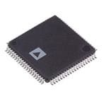
14-Bit, 160 MSPS, 2×/4×/8× Interpolating Dual TxDAC+® Digital-to-Analog Converter AD9775 FEATURES Versatile input data interface Twos complement/straight binary data coding 14-bit resolution, 160 MSPS/400 MSPS input/output Dual-port or single-port interleaved input data data rate Single 3.3 V supply operation Selectable 2×/4×/8× interpolating filter Power dissipation: 1.2 W @ 3.3 V typical Programmable channel gain and offset adjustment On-chip, 1.2 V reference f/4, f/8 digital quadrature modulation capability S S 80-lead, thin quad flat package, exposed pad (TQFP_EP) Direct IF transmission mode for 70 MHz + IFs Enables image rejection architecture APPLICATIONS Fully compatible SPI® port Communications Excellent ac performance Analog quadrature modulation architecture SFDR: −71 dBc @ 2 MHz to 35 MHz 3G, multicarrier GSM, TDMA, CDMA systems W-CDMA ACPR: −71 dB @ IF = 19.2 MHz Broadband wireless, point-to-point microwave radios Internal PLL clock multiplier Instrumentation/ATE Selectable internal clock divider Versatile clock input Differential/single-ended sine wave or TTL/CMOS/LVPECL compatible FUNCTIONAL BLOCK DIAGRAM IDAC COS AD9775 HALF- HALF- HALF- GAIN OFFSET BAND BAND BAND DAC DAC DATA FILTER1* FILTER2* FILTER3* ASSEMBLER SIN IMAGE I AND Q 14 LATICH 16 16 16 16 fDAC/2, 4, 8 RDEBUJMYAEPOLCAD TDSEIAOSCN/ VREF GRAEII/NGQ/IO SDFTAFECSREST OFFSET NONINTERLEAVED MUX I OR INTERLEAVED SIN DATA Q 16 16 16 16 14 LATCH FILTER BYPASS COS WRITE MUX MUX SELECT CONTROL /2 IDAC IOUT (fDAC) CLOCK OUT /2 /2 /2 SPI INTERFACE AND PRESCALER DIFFERENTIAL CONTROL REGISTERS CLK PHASE DETECTOR AND VCO *HALF-BAND FILTERS ALSO CAN BE CONFIGURED FOR ZERO STUFFING ONLY PLL CLOCK MULTIPLIER AND CLOCK DIVIDER 02858-001 Figure 1. Rev. E Information furnished by Analog Devices is believed to be accurate and reliable. However, no responsibility is assumed by Analog Devices for its use, nor for any infringements of patents or other One Technology Way, P.O. Box 9106, Norwood, MA 02062-9106, U.S.A. rights of third parties that may result from its use. Specifications subject to change without notice. No license is granted by implication or otherwise under any patent or patent rights of Analog Devices. Tel: 781.329.4700 www.analog.com Trademarks and registered trademarks are the property of their respective owners. Fax: 781.461.3113 ©2006 Analog Devices, Inc. All rights reserved.
AD9775 TABLE OF CONTENTS Features..............................................................................................1 1R/2R Mode................................................................................25 Applications.......................................................................................1 Clock Input Configurations......................................................25 Functional Block Diagram..............................................................1 Programmable PLL....................................................................26 Revision History...............................................................................3 Power Dissipation.......................................................................27 General Description.........................................................................4 Sleep/Power-Down Modes........................................................28 Product Highlights.......................................................................4 Two-Port Data Input Mode......................................................28 Specifications.....................................................................................5 PLL Enabled, Two-Port Mode..................................................28 DC Specifications.........................................................................5 DATACLK Inversion..................................................................29 Dynamic Specifications...............................................................6 DATACLK Driver Strength.......................................................29 Digital Specifications...................................................................7 PLL Enabled, One-Port Mode..................................................29 Digital Filter Specifications.........................................................8 ONEPORTCLK Inversion.........................................................29 Absolute Maximum Ratings............................................................9 ONEPORTCLK Driver Strength..............................................30 ESD Caution..................................................................................9 IQ Pairing....................................................................................30 Thermal Resistance......................................................................9 PLL Disabled, Two-Port Mode.................................................30 Pin Configuration and Function Descriptions...........................10 PLL Disabled, One-Port Mode.................................................30 Typical Performance Characteristics...........................................12 Digital Filter Modes...................................................................31 Terminology....................................................................................17 Amplitude Modulation..............................................................31 Mode Control (via SPI Port).........................................................18 Modulation, No Interpolation..................................................32 Register Descriptions.....................................................................19 Modulation, Interpolation = 2×...............................................33 Address 0x00...............................................................................19 Modulation, Interpolation = 4×...............................................34 Address 0x01...............................................................................19 Modulation, Interpolation = 8×...............................................35 Address 0x02...............................................................................19 Zero Stuffing...............................................................................36 Address 0x03...............................................................................20 Interpolating (Complex Mix Mode)........................................36 Address 0x04...............................................................................20 Operations on Complex Signals...............................................36 Address 0x05, Address 0x09.....................................................20 Complex Modulation and Image Rejection of Baseband Address 0x06, Address 0x0A.....................................................20 Signals..........................................................................................37 Address 0x07, Address 0x0B.....................................................20 Image Rejection and Sideband Suppression of Modulated Carriers........................................................................................38 Address 0x08, Address 0x0C.....................................................20 Applying the Output Configurations...........................................42 Address 0x08, Address 0x0C.....................................................20 Unbuffered Differential Output, Equivalent Circuit.............42 Functional Description..................................................................21 Differential Coupling Using a Transformer............................42 Serial Interface for Register Control........................................21 Differential Coupling Using an Op Amp................................43 General Operation of the Serial Interface...............................21 Interfacing the AD9775 with the AD8345 Quadrature Instruction Byte..........................................................................22 Modulator....................................................................................43 Serial Interface Port Pin Descriptions.....................................22 Evaluation Board............................................................................44 MSB/LSB Transfers.....................................................................22 Outline Dimensions.......................................................................54 Notes on Serial Port Operation................................................22 Ordering Guide..........................................................................54 DAC Operation...........................................................................24 Rev. E | Page 2 of 56
AD9775 REVISION HISTORY 12/06—Rev. D to Rev. E 2/03—Rev. 0 to Rev. A Changes to Figure 52, Figure 54, Figure 55, and Figure 56.......29 Edits to Features...............................................................................1 Edits to DC Specifications..............................................................3 1/06—Rev. C to Rev. D Edits to Dynamic Specifications....................................................4 Updated Formatting..........................................................Universal Edits to Pin Function Descriptions...............................................8 Changes to Figure 32....................................................................22 Edits to Table I...............................................................................14 Changes to Figure 108..................................................................55 Edits to Register Description—Address 02h.............................15 Updated Outline Dimensions......................................................58 Edits to Register Description—Address 03h.............................16 Changes to Ordering Guide.........................................................58 Edits to Register Description—Address 07h, 0Bh....................16 6/04—Rev. B to Rev. C Edits to Equation 1........................................................................16 Updated Layout.................................................................Universal Edits to MSB/LSB Transfers.........................................................18 Changes to DC Specifications.......................................................5 Edits to Programmable PLL.........................................................21 Changes to Absolute Maximum Ratings......................................9 Added New Figure 14...................................................................22 Changes to the DAC Operation Section....................................25 Renumbered Figures 15–69.........................................................22 Inserted Figure 38..........................................................................25 Added Two-Port Data Input Mode Section...............................23 Changes to Figure 40....................................................................26 Edits to PLL Enabled, Two-Port Mode......................................24 Changes to Table 11......................................................................28 Edits to Figure 19..........................................................................24 Changes to Programmable PLL Section.....................................28 Edits to Figure 21..........................................................................25 Changes to Figures 49, 50, and 51...............................................29 Edits to PLL Disabled, Two-Port Mode.....................................25 Changes to the PLL Enabled, One-Port Mode Section............30 Edits to Figure 22..........................................................................25 Changes to the PLL Disabled, One-Port Mode Section...........31 Edits to Figure 23..........................................................................26 Changes to the Ordering Guide..................................................57 Edits to Figure 26a........................................................................27 Updated Outline Dimensions......................................................57 Edits to Complex Modulation and Image Rejection of Baseband 3/03—Rev. A to Rev. B Signals.............................................................................................31 Changes to Register Description—Address 04h.......................16 Edits to Evaluation Board............................................................39 Changes to Equation 1..................................................................16 Edits to Figures 56–59..................................................................40 Changes to Figure 8.......................................................................20 Replaced Figures 60–69................................................................42 Updated Outline Dimensions......................................................49 Rev. E | Page 3 of 56
AD9775 GENERAL DESCRIPTION The AD97751 is the 14-bit member of the AD977x pin- The AD9775 is manufactured on an advanced 0.35 micron compatible, high performance, programmable 2×/4×/8× CMOS process, operates from a single supply of 3.1 V to 3.5 V, interpolating TxDAC+ family. The AD977x family features a and consumes 1.2 W of power. serial port interface (SPI) that provides a high level of Targeted at wide dynamic range, multicarrier and multistandard programmability, thus allowing for enhanced system-level systems, the superb baseband performance of the AD9775 is options. These options include selectable 2×/4×/8× ideal for wideband CDMA, multicarrier CDMA, multicarrier interpolation filters; f/2, f/4, or f/8 digital quadrature S S S TDMA, multicarrier GSM, and high performance systems modulation with image rejection; a direct IF mode; employing high order QAM modulation schemes. The image programmable channel gain and offset control; programmable rejection feature simplifies and can help reduce the number of internal clock divider; straight binary or twos complement data signal band filters needed in a transmit signal chain. The direct interface; and a single-port or dual-port data interface. IF mode helps to eliminate a costly mixer stage for a variety of The selectable 2×/4×/8× interpolation filters simplify the communications systems. requirements of the reconstruction filters while simultaneously PRODUCT HIGHLIGHTS enhancing the pass-band noise/distortion performance of 1. The AD9775 is the 14-bit member of the AD977x pin- TxDAC+ devices. The independent channel gain and offset compatible, high performance, programmable 2×/4×/8× adjust registers allow the user to calibrate LO feedthrough and interpolating TxDAC+ family. sideband suppression errors associated with analog quadrature 2. Direct IF transmission capability for 70 MHz + IFs through modulators. The 6 dB of gain adjustment range can also be used a novel digital mixing process. to control the output power level of each DAC. 3. f/2, f/4, and f/8 digital quadrature modulation and user- S S S The AD9775 can perform fS/2, fS/4, and fS/8 digital modulation selectable image rejection to simplify/remove cascaded and image rejection when combined with an analog quadrature SAW filter stages. modulator. In this mode, the AD9775 accepts I and Q complex 4. A 2×/4×/8× user-selectable, interpolating filter eases data data (representing a single or multicarrier waveform), generates rate and output signal reconstruction filter requirements. a quadrature modulated IF signal along with its orthogonal 5. User-selectable, twos complement/straight binary data representation via its dual DACs, and presents these two coding. reconstructed orthogonal IF carriers to an analog quadrature 6. User-programmable, channel gain control over 1 dB range modulator to complete the image rejection upconversion in 0.01 dB increments. process. Another digital modulation mode (that is, the direct IF 7. User programmable channel offset control ±10% over the mode) allows the original baseband signal representation to be FSR. frequency translated such that pairs of images fall at multiples 8. Ultrahigh speed 400 MSPS DAC conversion rate. of one-half the DAC update rate. 9. Internal clock divider provides data rate clock for easy interfacing. The AD977x family includes a flexible clock interface that 10. Flexible clock input with single-ended or differential input, accepts differential or single-ended sine wave or digital logic CMOS, or 1 V p-p LO sine wave input capability. inputs. An internal PLL clock multiplier is included and 11. Low power: complete CMOS DAC operates on 1.2 W from generates the necessary on-chip high frequency clocks. It can a 3.1 V to 3.5 V single supply. The 20 mA full-scale current also be disabled to allow the use of a higher performance can be reduced for lower power operation and several sleep external clock source. An internal programmable divider functions are provided to reduce power during idle simplifies clock generation in the converter when using an periods. external clock source. A flexible data input interface allows for 12. On-chip voltage reference. The AD9775 includes a 1.20 V straight binary or twos complement formats and supports temperature compensated band gap voltage reference. single-port interleaved or dual-port data. 13. 80-lead, thin quad flat package, exposed pad (TQFP_EP). Dual high performance DAC outputs provide a differential current output programmable over a 2 mA to 20 mA range. 1 Protected by U.S. Patent Numbers 5,568,145; 5,689,257; and 5,703,519. Other patents pending. Rev. E | Page 4 of 56
AD9775 SPECIFICATIONS DC SPECIFICATIONS T to T , AVDD = 3.3 V, CLKVDD = 3.3 V, DVDD = 3.3 V, PLLVDD = 3.3 V, I = 20 mA, unless otherwise noted. MIN MAX OUTFS Table 1. Parameter Min Typ Max Unit RESOLUTION 14 Bits DC Accuracy1 Integral Nonlinearity −5 ±1.5 +5 LSB Differential Nonlinearity −3 ±1.0 +3 LSB ANALOG OUTPUT (for 1R and 2R Gain Setting Modes) Offset Error −0.02 ±0.01 +0.02 % of FSR Gain Error (with Internal Reference) −1.0 +1.0 % of FSR Gain Matching −1.0 ±0.1 +1.0 % of FSR Full-Scale Output Current2 2 20 mA Output Compliance Range −1.0 +1.25 V Output Resistance 200 kΩ Output Capacitance 3 pF Gain, Offset Cal DACs, Monotonicity Guaranteed REFERENCE OUTPUT Reference Voltage 1.14 1.20 1.26 V Reference Output Current3 100 nA REFERENCE INPUT Input Compliance Range 0.1 1.25 V Reference Input Resistance 7 kΩ Small Signal Bandwidth 0.5 MHz TEMPERATURE COEFFICIENTS Offset Drift 0 ppm of FSR/°C Gain Drift (with Internal Reference) 50 ppm of FSR/°C Reference Voltage Drift ±50 ppm/°C POWER SUPPLY AVDD Voltage Range 3.1 3.3 3.5 V Analog Supply Current (I )4 72.5 76 mA AVDD I in SLEEP Mode 23.3 26 mA AVDD CLKVDD Voltage Range 3.1 3.3 3.5 V Clock Supply Current (I )4 8.5 10.0 mA CLKVDD CLKVDD (PLL ON) Clock Supply Current (I ) 23.5 mA CLKVDD DVDD Voltage Range 3.1 3.3 3.5 V Digital Supply Current (I )4 34 41 mA DVDD Nominal Power Dissipation 380 410 mW P 5 1.75 W DIS P IN PWDN 6.0 mW DIS Power Supply Rejection Ratio—AVDD ±0.4 % of FSR/V OPERATING RANGE −40 +85 °C 1 Measured at IOUTA driving a virtual ground. 2 Nominal full-scale current, IOUTFS, is 32 × the IREF current. 3 Use an external amplifier to drive any external load. 4 100 MSPS fDAC with fOUT = 1 MHz, all supplies = 3.3 V, no interpolation, no modulation. 5 400 MSPS fDAC = 50 MSPS, fS/2 modulation, PLL enabled. Rev. E | Page 5 of 56
AD9775 DYNAMIC SPECIFICATIONS T to T , AVDD = 3.3 V, CLKVDD = 3.3 V, DVDD = 3.3 V, PLLVDD = 0 V, I = 20 mA, interpolation = 2×, differential MIN MAX OUTFS transformer-coupled output, 50 Ω doubly terminated, unless otherwise noted. Table 2. Parameter Min Typ Max Unit DYNAMIC PERFORMANCE Maximum DAC Output Update Rate (f ) 400 MSPS DAC Output Settling Time (t ) to 0.025% 11 ns ST Output Rise Time 10% to 90%1 0.8 ns Output Fall Time 10% to 90%1 0.8 ns Output Noise, I = 20 mA 50 pA/√Hz OUTFS AC LINEARITY—BASEBAND MODE Spurious-Free Dynamic Range (SFDR) to Nyquist (f = 0 dBFS) OUT f = 100 MSPS, f = 1 MHz 71 84.5 dBc DATA OUT f = 65 MSPS, f = 1 MHz 84 dBc DATA OUT f = 65 MSPS, f = 15 MHz 80 dBc DATA OUT f = 78 MSPS, f = 1 MHz 84 dBc DATA OUT f = 78 MSPS, f = 15 MHz 80 dBc DATA OUT f = 160 MSPS, f = 1 MHz 82 dBc DATA OUT f = 160 MSPS, f = 15 MHz 80 dBc DATA OUT Spurious-Free Dynamic Range Within a 1 MHz Window f = 0 dBFS, f = 100 MSPS, f = 1 MHz 73 91.3 dBc OUT DATA OUT Two-Tone Intermodulation (IMD) to Nyquist (f = f = −6 dBFS) OUT1 OUT2 f = 65 MSPS, f = 10 MHz; f = 11 MHz 81 dBc DATA OUT1 OUT2 f = 65 MSPS, f = 20 MHz; f = 21 MHz 76 dBc DATA OUT1 OUT2 f = 78 MSPS, f = 10 MHz; f = 11 MHz 81 dBc DATA OUT1 OUT2 f = 78 MSPS, f = 20 MHz; f = 21 MHz 76 dBc DATA OUT1 OUT2 f = 160 MSPS, f = 10 MHz; f = 11 MHz 81 dBc DATA OUT1 OUT2 f = 160 MSPS, f = 20 MHz; f = 21 MHz 76 dBc DATA OUT1 OUT2 Total Harmonic Distortion (THD) f = 100 MSPS, f = 1 MHz; 0 dBFS −71 −82.5 dB DATA OUT Signal-to-Noise Ratio (SNR) f = 78 MSPS, f = 5 MHz; 0 dBFS 76 dB DATA OUT f = 160 MSPS, f = 5 MHz; 0 dBFS 74 dB DATA OUT Adjacent Channel Power Ratio (ACPR) W-CDMA with 3.84 MHz BW, 5 MHz Channel Spacing IF = Baseband, f = 76.8 MSPS 71 dBc DATA IF = 19.2 MHz, f = 76.8 MSPS 71 dBc DATA Four-Tone Intermodulation 21 MHz, 22 MHz, 23 MHz, and 24 MHz at −12 dBFS (f = MSPS, Missing Center) 75 dBFS DATA AC LINEARITY—IF MODE Four-Tone Intermodulation at IF = 200 MHz 201 MHz, 202 MHz, 203 MHz, and 204 MHz at −12 dBFS (f = 160 MSPS, f = 320 MHz) 72 dBFS DATA DAC 1 Measured single-ended into 50 Ω load. Rev. E | Page 6 of 56
AD9775 DIGITAL SPECIFICATIONS T to T , AVDD = 3.3 V, CLKVDD = 3.3 V, PLLVDD = 0 V, DVDD = 3.3 V, I = 20 mA, unless otherwise noted. MIN MAX OUTFS Table 3. Parameter Min Typ Max Unit DIGITAL INPUTS Logic 1 Voltage 2.1 3 V Logic 0 Voltage 0 0.9 V Logic 1 Current −10 +10 μA Logic 0 Current −10 +10 μA Input Capacitance 5 pF CLOCK INPUTS Input Voltage Range 0 3 V Common-Mode Voltage 0.75 1.5 2.25 V Differential Voltage 0.5 1.5 V SERIAL CONTROL BUS Maximum SCLK Frequency (f ) 15 MHz SLCK Minimum Clock Pulse Width High (t ) 30 ns PWH Minimum Clock Pulse Width Low (t ) 30 ns PWL Maximum Clock Rise/Fall Time 1 ms Minimum Data/Chip Select Setup Time (t ) 25 ns DS Minimum Data Hold Time (t ) 0 ns DH Maximum Data Valid Time (t ) 30 ns DV RESET Pulse Width 1.5 ns Inputs (SDI, SDIO, SCLK, CSB) Logic 1 Voltage 2.1 3 V Logic 0 Voltage 0 0.9 V Logic 1 Current −10 +10 μA Logic 0 Current −10 +10 μA Input Capacitance 5 pF SDIO Output Logic 1 Voltage DRVDD − 0.6 V Logic 0 Voltage 0.4 V Logic 1 Current 30 50 mA Logic 0 Current 30 50 mA Rev. E | Page 7 of 56
AD9775 DIGITAL FILTER SPECIFICATIONS 20 Table 4. Half-Band Filter No. 1 (43 Coefficients) Tap Coefficient 0 1, 43 8 2, 42 0 S) –20 F B 3, 41 −29 d N ( –40 4, 40 0 O TI 5, 39 67 UA –60 N 6, 38 0 E T T 7, 37 −134 A –80 8, 36 0 –100 9, 35 244 10, 34 0 –120 1112,, 3332 −0 4 14 0 fOUT0 (.N5ORMALIZED1 T.0O INPUT DATA1 .R5ATE) 2.0 02858-002 13, 31 673 Figure 2. 2× Interpolating Filter Response 14, 30 0 15, 29 −1079 20 16, 28 0 17, 27 1772 0 18, 26 0 19, 25 −3280 FS) –20 B d 20, 24 0 N ( –40 O 21, 23 10,364 TI A 22 16,384 NU –60 E T T A –80 Table 5. Half-Band Filter No. 2 (19 Coefficients) Tap Coefficient –100 1, 19 19 2, 18 0 –120 34,, 1176 −0 1 20 0 fOUT0 (.N5ORMALIZED1 T.0O INPUT DATA1 .R5ATE) 2.0 02858-003 5, 15 438 Figure 3. 4× Interpolating Filter Response 6, 14 0 20 7, 13 −1288 8, 12 0 0 9, 11 5,047 10 8,192 S) –20 F B d Table 6. Half-Band Filter No. 3 (11 Coefficients) N ( –40 O TI Tap Coefficient A U –60 N 1, 11 7 E T T 2, 10 0 A –80 3, 9 −53 –100 4, 8 0 5, 7 302 –120 6 512 0 fOUT 2(NORMALIZED T4O INPUT DATA6 RATE) 8 02858-004 Figure 4. 8× Interpolating Filter Response Rev. E | Page 8 of 56
AD9775 ABSOLUTE MAXIMUM RATINGS Table 7. Parameter With Respect To Rating AVDD, DVDD, CLKVDD AGND, DGND, CLKGND −0.3 V to +4.0 V AVDD, DVDD, CLKVDD AVDD, DVDD, CLKVDD −4.0 V to +4.0 V AGND, DGND, CLKGND AGND, DGND, CLKGND −0.3 V to +0.3 V REFIO, FSADJ1/FSADJ2 AGND −0.3 V to AVDD + 0.3 V I , I AGND −1.0 V to AVDD + 0.3 V OUTA OUTB P1B13 to P1B0, P2B13 to P2B0, RESET DGND −0.3 V to DVDD + 0.3 V DATACLK, PLL_LOCK DGND −0.3 V to DVDD + 0.3 V CLK+, CLK– CLKGND −0.3 V to CLKVDD + 0.3 V LPF CLKGND −0.3 V to CLKVDD + 0.3 V SPI_CSB, SPI_CLK, SPI_SDIO, SPI_SDO DGND −0.3 V to DVDD + 0.3 V Junction Temperature 125°C Storage Temperature −65°C to +150°C Lead Temperature (10 sec) 300°C Stresses above those listed under Absolute Maximum Ratings THERMAL RESISTANCE may cause permanent damage to the device. This is a stress θ is specified for the worst-case conditions, that is, a device rating only; functional operation of the device at these or any JA soldered in a circuit board for surface-mount packages. other conditions above those indicated in the operational section of this specification is not implied. Exposure to absolute Table 8. Thermal Resistance maximum rating conditions for extended periods may affect Package Type θ Unit JA device reliability. 80-Lead Thin Quad Flat Package 23.5 °C/W ESD CAUTION (TQFP_EP), Exposed Pad Rev. E | Page 9 of 56
AD9775 PIN CONFIGURATION AND FUNCTION DESCRIPTIONS DD ND DD ND DD ND ND TA1 TB1ND ND TA2 TB2ND ND DD ND DD ND DD AV AG AV AG AV AG AG IOUIOUAG AG IOUIOUAG AG AV AG AV AG AV 80 79 78 77 76 75 74 73 72 71 70 69 68 67 66 65 64 63 62 61 CLKVDD 1 60 FSADJ1 LPF 2 PIN 1 59 FSADJ2 CLKVDD 3 58 REFIO CLKGND 4 57 RESET CLK+ 5 56 SPI_CSB CLK– 6 55 SPI_CLK CLKGND 7 54 SPI_SDIO AD9775 DATACLK/PLL_LOCK 8 53 SPI_SDO TxDAC+ DGND 9 TOP VIEW 52 DGND DVDD 10 (Not to Scale) 51 DVDD P1B13 (MSB) 11 50 NC P1B12 12 49 NC P1B11 13 48 P2B0 (LSB) P1B10 14 47 P2B1 P1B9 15 46 P2B2 P1B8 16 45 P2B3 DGND 17 44 DGND DVDD 18 43 DVDD P1B7 19 42 P2B4 P1B6 20 41 P2B5 21 22 23 24 25 26 27 28 29 30 31 32 33 34 35 36 37 38 39 40 NC = NO CONNECT P1B5 P1B4 P1B3 P1B2 DGND DVDD P1B1 P1B0 (LSB) NC NC IQSEL/P2B13 (MSB) ONEPORTCLK/P2B12 P2B11 P2B10 DGND DVDD P2B9 P2B8 P2B7 P2B6 02858-005 Figure 5. Pin Configuration Rev. E | Page 10 of 56
AD9775 Table 9. Pin Function Descriptions Pin No. Mnemonic Description 1, 3 CLKVDD Clock Supply Voltage. 2 LPF PLL Loop Filter. 4, 7 CLKGND Clock Supply Common. 5 CLK+ Differential Clock Input. 6 CLK− Differential Clock Input. 8 DATACLK/PLL_LOCK With the PLL enabled, this pin indicates the state of the PLL. A read of a Logic 1 indicates the PLL is in the locked state. Logic 0 indicates the PLL has not achieved lock. This pin may also be programmed to act as either an input or output (Address 02h, Bit 3) DATACLK signal running at the input data rate. 9, 17, 25, 35, 44, 52 DGND Digital Common. 10, 18, 26, 36, 43, 51 DVDD Digital Supply Voltage. 11 to 16, 19 to 24, 27, 28 P1B13 (MSB) to P1B0 Port 1 Data Inputs. (LSB) 29, 30, 49, 50 NC No Connect. 31 IQSEL/P2B13 (MSB) In one-port mode, IQSEL = 1 followed by a rising edge of the differential input clock latches the data into the I channel input register. IQSEL = 0 latches the data into the Q channel input register. In two-port mode, this pin becomes the Port 2 MSB. 32 ONEPORTCLK/P2B12 With the PLL disabled and the AD9775 in one-port mode, this pin becomes a clock output that runs at twice the input data rate of the I and Q channels. This allows the AD9775 to accept and demux interleaved I and Q data to the I and Q input registers. 33, 34, 37 to 42, 45 to 48 P2B11 to P2B0 (LSB) Port 2 Data Inputs. 53 SPI_SDO In the case where SDIO is an input, SDO acts as an output. When SDIO becomes an output, SDO enters a High-Z state. This pin can also be used as an output for the data rate clock. For more information, see the Two-Port Data Input Mode section. 54 SPI_SDIO Bidirectional Data Pin. Data direction is controlled by Bit 7 of Register Address 0x00. The default setting for this bit is 0, which sets SDIO as an input. 55 SPI_CLK Data input to the SPI port is registered on the rising edge of SPI_CLK. Data output on the SPI port is registered on the falling edge. 56 SPI_CSB Chip Select/SPI Data Synchronization. On momentary logic high, resets SPI port logic and initializes instruction cycle. 57 RESET Logic 1 resets all of the SPI port registers, including Address 0x00, to their default values. A software reset can also be done by writing a Logic 1 to SPI Register 00h, Bit 5. However, the software reset has no effect on the bit in Address 0x00. 58 REFIO Reference Output, 1.2 V Nominal. 59 FSADJ2 Full-Scale Current Adjust, Q Channel. 60 FSADJ1 Full-Scale Current Adjust, I Channel. 61, 63, 65, 76, 78, 80 AVDD Analog Supply Voltage. 62, 64, 66, 67, 70, 71, AGND Analog Common. 74, 75, 77, 79 68, 69 I , I Differential DAC Current Outputs, Q Channel. OUTB2 OUTA2 72, 73 I ,I Differential DAC Current Outputs, I Channel. OUTB1 OUTA1 Rev. E | Page 11 of 56
AD9775 TYPICAL PERFORMANCE CHARACTERISTICS T = 25°C, AVDD = 3.3 V, CLKVDD = 3.3 V, DVDD = 3.3 V, I = 20 mA, interpolation = 2×, differential transformer-coupled output, OUTFS 50 Ω doubly terminated, unless otherwise noted. 10 10 0 0 –10 –10 –20 –20 m) m) dB –30 dB –30 E ( E ( UD –40 UD –40 T T PLI –50 PLI –50 M M A –60 A –60 –70 –70 –80 –80 –90 –90 0 FREQUE6N5CY (MHz) 130 02858-006 0 50FREQUENCY (MH10z0) 150 02858-009 Figure 6. Single-Tone Spectrum @ fDATA = 65 MSPS with fOUT = fDATA/3 Figure 9. Single-Tone Spectrum @ fDATA = 78 MSPS with fOUT = fDATA/3 90 90 0dBFS 0dBFS 85 85 –6dBFS 80 80 75 75 c) c) dB –12dBFS dB –12dBFS DR ( 70 DR ( 70 –6dBFS F F S 65 S 65 60 60 55 55 50 50 0 5 10FREQUE1N5CY (MHz)20 25 30 02858-007 0 5 10FREQUE1N5CY (MHz)20 25 30 02858-010 Figure 7. In-Band SFDR vs. fOUT @ fDATA = 65 MSPS Figure 10. In-Band SFDR vs. fOUT @ fDATA = 78 MSPS 90 90 –6dBFS 85 85 –6dBFS 0dBFS 80 80 0dBFS 75 75 c) c) B B d d R ( 70 R ( 70 FD –12dBFS FD –12dBFS S 65 S 65 60 60 55 55 50 50 0 5 10FREQUE1N5CY (MHz)20 25 30 02858-008 0 5 10FREQUE1N5CY (MHz)20 25 30 02858-011 Figure 8. Out-of-Band SFDR vs. fOUT @ fDATA = 65 MSPS Figure 11. Out-of-Band SFDR vs. fOUT @ fDATA = 78 MSPS Rev. E | Page 12 of 56
AD9775 10 90 –6dBFS –3dBFS 0 85 –10 80 –20 m) UDE (dB ––4300 D (dBc) 7705 0dBFS MPLIT –50 IM 65 A –60 60 –70 55 –80 –90 50 0 100FREQUENCY (MH20z0) 300 02858-012 0 5 10FREQUE1N5CY (MHz)20 25 30 02858-015 Figure 12. Single-Tone Spectrum @ fDATA = 160 MSPS with fOUT = fDATA/3 Figure 15. Third-Order IMD Products vs. fOUT @ fDATA = 65 MSPS 90 90 –6dBFS 0dBFS –6dBFS 85 85 0dBFS 80 80 75 75 c) c) B B d d R ( 70 D ( 70 D –12dBFS M –3dBFS F I S 65 65 60 60 55 55 50 50 0 10 FR2E0QUENCY (M30Hz) 40 50 02858-013 0 5 10FREQUE1N5CY (MHz)20 25 30 02858-016 Figure 13. In-Band SFDR vs. fOUT @ fDATA = 160 MSPS Figure 16. Third-Order IMD Products vs. fOUT @ fDATA = 78 MSPS 90 90 85 85 –6dBFS 80 80 –6dBFS 75 75 dBc) 0dBFS dBc) –3dBFS R ( 70 D ( 70 SFD 65 IM 65 0dBFS 60 60 –12dBFS 55 55 50 50 0 10 FR2E0QUENCY (M30Hz) 40 50 02858-014 0 10 20FREQUE3N0CY (MHz)40 50 60 02858-017 Figure 14. Out-of-Band SFDR vs. fOUT @ fDATA = 160 MSPS Figure 17. Third-Order IMD Products vs. fOUT @ fDATA = 160 MSPS Rev. E | Page 13 of 56
AD9775 90 90 8× –3dBFS 85 85 80 80 0dBFS 75 75 Bc) 4× Bc) –6dBFS d 2× d MD ( 70 1× DR ( 70 I 65 SF 65 60 60 55 55 50 50 0 10 20FREQUE3N0CY (MHz)40 50 60 02858-018 3.1 3.2 AV3D.D3 (V) 3.4 3.5 02858-021 Figure 18. Third-Order IMD Products vs. fOUT and Interpolation Rate, Figure 21. Third-Order IMD Products vs. AVDD @ fOUT = 10 MHz, 1× fDATA = 160 MSPS, 2× fDATA = 160 MSPS, 4× fDATA = 80 MSPS, fDAC = 320 MSPS, fDATA = 160 MSPS 8× fDATA = 50 MSPS 90 90 4× 8× 85 85 80 80 Bc) 75 2× 1× B) 75 PLL OFF D (d 70 R (d 70 M N I S 65 65 60 60 PLL ON 55 55 50 50 –15 –10 AOUT (dBFS) –5 0 02858-019 0 5I0NPUT DATA RATE1 (0M0SPS) 150 02858-022 Figure 19. Third-Order IMD Products vs. AOUT and Interpolation Rate, Figure 22. SNR vs. Data Rate for fOUT = 5 MHz fDATA = 50 MSPS for All Cases, 1× fDAC = 50 MSPS, 2× fDAC = 100 MSPS, 4× fDAC = 200 MSPS, 8× fDAC = 400 MSPS 90 90 78MSPS 0dBFS 85 85 80 80 75 75 Bc) Bc) fDATA = 65MSPS 160MSPS DR (d 70 –12dBFS –6dBFS DR (d 70 SF 65 SF 65 60 60 55 55 50 50 3.1 3.2 AV3D.D3 (V) 3.4 3.5 02858-020 –50 0TEMPERATURE (°C5)0 100 02858-023 Figure 20. SFDR vs. AVDD @ fOUT = 10 MHz, fDAC = 320 MSPS, fDATA = 160 MSPS Figure 23. SFDR vs. Temperature @ fOUT = fDATA/11 Rev. E | Page 14 of 56
AD9775 0 0 –10 –10 –20 –20 –30 –30 m) m) dB –40 dB –40 E ( E ( D –50 D –50 U U T T PLI –60 PLI –60 M M A A –70 –70 –80 –80 –90 –90 –100 –100 0 50FREQUENCY (MHz1)00 150 02858-024 0 5 10 15 FR2E0QUE2N5CY (M30Hz) 35 40 45 50 02858-027 Figure 24. Single-Tone Spurious Performance, fOUT = 10 MHz, Figure 27. Two-Tone IMD Performance, fDATA = 150 MSPS, Interpolation = 4× fDATA = 150 MSPS, No Interpolation 0 0 –10 –20 –20 –30 m) m) MPLITUDE (dB ––6400 MPLITUDE (dB –––654000 A A –70 –80 –80 –90 –100 –100 0 10 FR2E0QUENCY (M30Hz) 40 50 02858-025 0 50 100FREQUE1N50CY (MHz2)00 250 300 02858-028 Figure 25. Two-Tone IMD Performance, fDATA = 150 MSPS, No Interpolation Figure 28. Single-Tone Spurious Performance, fOUT = 10 MHz, fDATA = 80 MSPS, Interpolation = 4× 0 0 –10 –10 –20 –20 –30 –30 m) m) E (dB –40 E (dB –40 UD –50 UD –50 PLIT –60 PLIT –60 M M A –70 A –70 –80 –80 –90 –90 –100 –100 0 50 100FREQUE1N50CY (MHz2)00 250 300 02858-026 0 5 FR1E0QUENCY (M15Hz) 20 25 02858-029 Figure 26. Single-Tone Spurious Performance, fOUT = 10 MHz, Figure 29. Two-Tone IMD Performance, fOUT = 10 MHz, fDATA = 150 MSPS, Interpolation = 2× fDATA = 50 MSPS, Interpolation = 8× Rev. E | Page 15 of 56
AD9775 0 0 –10 –20 –20 –30 m) m) –40 dB –40 dB E ( E ( UD –50 UD –60 T T PLI –60 PLI M M A A –80 –70 –80 –100 –90 –100 –120 0 100 FREQUE2N00CY (MHz) 300 400 02858-030 0 20 FREQUE4N0CY (MHz) 60 80 02858-031 Figure 30. Single-Tone Spurious Performance, fOUT = 10 MHz, Figure 31. Eight-Tone IMD Performance, fDATA = 160 MSPS, fDATA = 50 MSPS, Interpolation = 8× Interpolation = 8× Rev. E | Page 16 of 56
AD9775 TERMINOLOGY Monotonicity Adjacent Channel Power Ratio (ACPR) A DAC is monotonic if the output either increases or remains A ratio in dBc between the measured power within a channel constant as the digital input increases. relative to its adjacent channel. Offset Error Complex Image Rejection The deviation of the output current from the ideal of 0 is called In a traditional two-part upconversion, two images are created offset error. For I , 0 mA output is expected when the inputs around the second IF frequency. These images are redundant OUTA are all 0. For I , 0 mA output is expected when all inputs are and have the effect of wasting transmitter power and system OUTB set to 1. bandwidth. By placing the real part of a second complex modulator in series with the first complex modulator, either the Output Compliance Range upper or lower frequency image near the second IF can be The range of allowable voltage at the output of a current output rejected. DAC. Operation beyond the maximum compliance limits may cause either output stage saturation or breakdown, resulting in Complex Modulation nonlinear performance. The process of passing the real and imaginary components of a signal through a complex modulator (transfer function = ejωt = Pass Band cosωt + jsinωt) and realizing real and imaginary components Frequency band in which any input applied therein passes on the modulator output. unattenuated to the DAC output. Differential Nonlinearity (DNL) Power Supply Rejection DNL is the measure of the variation in analog value, normalized The maximum change in the full-scale output as the supplies to full scale, associated with a 1 LSB change in digital input are varied from minimum to maximum specified voltages. code. Settling Time Gain Error The time required for the output to reach and remain within a The difference between the actual and ideal output span. The specified error band about its final value, measured from the actual span is determined by the output when all inputs are set start of the output transition. to 1 minus the output when all inputs are set to 0. Signal-to-Noise Ratio (SNR) Glitch Impulse SNR is the ratio of the rms value of the measured output signal Asymmetrical switching times in a DAC give rise to undesired to the rms sum of all other spectral components below the output transients that are quantified by a glitch impulse. It is Nyquist frequency, excluding the first six harmonics and dc. specified as the net area of the glitch in pV-s. The value for SNR is expressed in decibels. Group Delay Spurious-Free Dynamic Range Number of input clocks between an impulse applied at the The difference, in dB, between the rms amplitude of the output device input and the peak DAC output current. A half-band FIR signal and the peak spurious signal over the specified filter has constant group delay over its entire frequency range. bandwidth. Impulse Response Stop-Band Rejection Response of the device to an impulse applied to the input. The amount of attenuation of a frequency outside the pass band applied to the DAC, relative to a full-scale signal applied at the Interpolation Filter DAC input within the pass band. If the digital inputs to the DAC are sampled at a multiple rate of f (interpolation rate), a digital filter can be constructed with Temperature Drift DATA a sharp transition band near fDATA/2. Images that would Temperature drift is specified as the maximum change from the typically appear around f (output data rate) can be greatly ambient (25°C) value to the value at either T or T . For DAC MIN MAX suppressed. offset and gain drift, the drift is reported in ppm of full-scale range (FSR) per °C. For reference drift, the drift is reported in Linearity Error ppm per °C. (Also called integral nonlinearity or INL.) It is defined as the maximum deviation of the actual analog output from the ideal Total Harmonic Distortion (THD) output, determined by a straight line drawn from zero scale to THD is the ratio of the rms sum of the first six harmonic full scale. components to the rms value of the measured fundamental. It is expressed as a percentage or in decibels (dB). Rev. E | Page 17 of 56
AD9775 MODE CONTROL (VIA SPI PORT) Table 10. Mode Control via SPI Port1 Address Bit 7 Bit 6 Bit 5 Bit 4 Bit 3 Bit 2 Bit 1 Bit 0 0x00 SDIO LSB, MSB Software Sleep Mode Power-Down 1R/2R Mode PLL_LOCK Bidirectional First, 0 = MSB Reset on Logic 1 Mode Logic 1 DAC Output Indicator 0 = Input 1 = LSB Logic 1 Shuts Down Shuts Down All Current Set 1 = I/O the DAC Digital and by One or Output Analog Two External Currents Functions Resistors 0 = 2R, 1 = 1R 0x 01 Filter Filter Modulation Modulation 0 = No Zero 1 = Real 0 = e−jωt DATACLK/ Interpolation Interpolation Mode Mode Stuffing on Mix Mode 1 = e+jωt PLL_LOCK2 Rate (1×, 2×, Rate (1×, 2×, 4×, (None, fS/2, (None, fS/2, Interpolation 0 = Complex Select 4×, 8×) 8×) fS/4, fS/8) fS/4, fS/8) Filters, Logic 1 Mix Mode 0 = PLLLOCK Enables Zero 1 = DATACLK Stuffing. 0x 02 0 = Signed 0 = Two-Port DATACLK DATACLK ONEPORTCLK IQSEL Invert Q First Input Data Mode Driver Invert Invert 0 = No Invert 0 = I First 1 = Unsigned 1 = One-Port Strength 0 = No Invert 0 = No Invert 1 = Invert 1 = Q First Mode 1 = Invert 1 = Invert 0x 03 Data Rate PLL Divide PLL Divide Clock Output2 (Prescaler) (Prescaler) Ratio Ratio 0x 04 0 = PLL OFF2 0 = Automatic PLL Charge PLL Charge PLL Charge 1 = PLL ON Charge Pump Pump Pump Pump Control Control, 1 = Control Control Programmable 0x 05 IDAC Fine Gain Adjustment 0x 06 IDAC Coarse Gain Adjustment 0x 07 IDAC Offset IDAC Offset IDAC Offset IDAC Offset IDAC Offset IDAC Offset IDAC Offset IDAC Offset Adjustment Adjustment Adjustment Adjustment Adjustment Adjustment Adjustment Adjustment Bit 9 Bit 8 Bit 7 Bit 6 Bit 5 Bit 4 Bit 3 Bit 2 0x 08 IDAC I IDAC Offset IDAC Offset OFFSET Direction Adjustment Adjustment 0 = I Bit 1 Bit 0 OFFSET on I OUTA 1 = I OFFSET on I OUTB 0x 09 QDAC Fine Gain Adjustment 0x 0A QDAC Coarse Gain Adjustment 0x 0B QDAC Offset QDAC Offset QDAC Offset QDAC Offset QDAC Offset QDAC Offset QDAC Offset QDAC Offset Adjustment Adjustment Adjustment Adjustment Adjustment Adjustment Adjustment Adjustment Bit 9 Bit 8 Bit 7 Bit 6 Bit 5 Bit 4 Bit 3 Bit 2 0x 0C QDAC I QDAC Offset QDAC Offset OFFSET Direction Adjustment Adjustment 0 = I Bit 1 Bit 0 OFFSET on I OUTA 1 = I OFFSET on I OUTB 0x 0D Version Register 1 Default values are shown in bold. 2 See the Two-Port Data Input Mode section. Rev. E | Page 18 of 56
AD9775 REGISTER DESCRIPTIONS ADDRESS 0x00 Bit 3: Logic 1 enables zero-stuffing mode for interpolation filters. Bit 7: Logic 0 (default) causes the SPI_SDIO pin to act as an Bit 2: Default (1) enables the real mix mode. The I and Q data input during the data transfer (Phase 2) of the communications channels are individually modulated by f/2, f/4, or f/8 after S S S cycle. When set to 1, SPI_SDIO can act as an input or output, the interpolation filters. However, no complex modulation is depending on Bit 7 of the instruction byte. done. In the complex mix mode (Logic 0), the digital Bit 6: Logic 0 (default) determines the direction (LSB/MSB modulators on the I and Q data channels are coupled to create a first) of the communications and data transfer communications digital complex modulator. When the AD9775 is applied in cycles. Refer to the MSB/LSB Transfers section for more details. conjunction with an external quadrature modulator, rejection can be achieved of either the higher or lower frequency image Bit 5: Writing 1 to this bit resets the registers to their default around the second IF frequency (that is, the LO of the analog values and restarts the chip. The RESET bit always reads back 0. quadrature modulator external to the AD9775) according to the Register Address 0x00 bits are not cleared by this software reset. bit value of Register 0x01, Bit 1. However, a high level at the RESET pin forces all registers, including those in Address 0x00, to their default state. Bit 1: Logic 0 (default) causes the complex modulation to be of the form e− jωt, resulting in the rejection of the higher frequency Bit 4: Sleep Mode. A Logic 1 to this bit shuts down the DAC image when the AD9775 is used with an external quadrature output currents. modulator. A Logic 1 causes the modulation to be of the form Bit 3: Power Down. Logic 1 shuts down all analog and digital e+jωt, which causes rejection of the lower frequency image. functions except for the SPI port. Bit 0: In two-port mode, a Logic 0 (default) causes Pin 8 to act Bit 2: 1R/2R Mode. The default (0) places the AD9775 in two- as a lock indicator for the internal PLL. A Logic 1 in this register resistor mode. In this mode, the I currents for the I and Q REF causes Pin 8 to act as a DATACLK. For more information, see DAC references are set separately by the R resistors on FSADJ1 SET the Two-Port Data Input Mode section. and FSADJ2 (Pin 60 and Pin 59). In 2R mode, assuming the coarse ADDRESS 0x02 gain setting is full scale and the fine gain setting is zero, I = 32 × V /FSADJ1 and I = 32 × V /FSADJ2. Bit 7: Logic 0 (default) causes data to be accepted on the inputs FULLSCALE1 REF FULLSCALE2 REF With this bit set to 1, the reference currents for both I and Q as twos complement binary. Logic 1 causes data to be accepted DACs are controlled by a single resistor on Pin 60. I in as straight binary. FULLSCALE one-resistor mode for both of the I and Q DACs is half of what Bit 6: Logic 0 (default) places the AD9775 in two-port mode. it would be in 2R mode, assuming all other conditions (R , SET I and Q data enters the AD9775 via Ports 1 and 2, respectively. register settings) remain unchanged. The full-scale current of A Logic 1 places the AD9775 in one-port mode in which each DAC can still be set to 20 mA by choosing a resistor of half interleaved I and Q data is applied to Port 1. See Table 9 for the value of the R value used in 2R mode. SET detailed information on how to use the DATACLK/PLL_LOCK, Bit 1: PLL_LOCK Indicator. When the PLL is enabled, reading IQSEL, and ONEPORTCLK modes. this bit gives the status of the PLL. A Logic 1 indicates the PLL Bit 5: DATACLK Driver Strength. With the internal PLL is locked. A Logic 0 indicates an unlocked state. disabled and this bit set to Logic 0, it is recommended that ADDRESS 0x01 DATACLK be buffered. When this bit is set to Logic 1, DATACLK acts as a stronger driver capable of driving small Bit 7 and Bit 6: This is the filter interpolation rate according to capacitive loads. the following table. Bit 4: Logic 0 (default). A value of 1 inverts DATACLK at Pin 8. Table 11. 00 1× Bit 2: Logic 0 (default). A value of 1 inverts ONEPORTCLK at 01 2× Pin 32. 10 4× Bit 1: Logic 0 (default) causes IQSEL = 0 to direct input data to 11 8× the I channel, while IQSEL = 1 directs input data to the Q channel. Bit 5 and Bit 4: This is the modulation mode according to the following table. Bit 0: Logic 0 (default) defines IQ pairing as IQ, IQ… while programming a Logic 1 causes the pair ordering to be QI, QI… Table 12. 00 None 01 f/2 S 10 f/4 S 11 f/8 S Rev. E | Page 19 of 56
AD9775 ADDRESS 0x03 ADDRESS 0x05, ADDRESS 0x09 Bit 7: Allows the data rate clock (divided down from the DAC Bit 7 to Bit 0: These bits represent an 8-bit binary number clock) to be output at either the DATACLK/PLL_LOCK pin (Bit 7 MSB) that defines the fine gain adjustment of the I (0x05) (Pin 8) or at the SPI_SDO pin (Pin 53). The default of 0 in this and Q (0x09) DAC, according to Equation 1. register enables the data rate clock at DATACLK/ PLL_LOCK, ADDRESS 0x06, ADDRESS 0x0A while a 1 in this register causes the data rate clock to be output Bit 3 to Bit 0: These bits represent a 4-bit binary number (Bit 3 at SPI_SDO. For more information, see the Two-Port Data MSB) that defines the coarse gain adjustment of the I (0x06) Input Mode section. and Q (0x0A) DACs, according to Equation 1. Bit 1 and Bit 0: Setting this divide ratio to a higher number ADDRESS 0x07, ADDRESS 0x0B allows the VCO in the PLL to run at a high rate (for best performance) while the DAC input and output clocks run Bit 7 to Bit 0: These bits are used in conjunction with Address substantially slower. The divider ratio is set according to the 0x08, 0x0C, Bit 1 and Bit 0. following table. ADDRESS 0x08, ADDRESS 0x0C Table 13. Bit 1 and Bit 0: The 10 bits from these two address pairs 00 ÷1 (0x07, 0x08 and 0x0B, 0x0C) represent a 10-bit binary number 01 ÷2 that defines the offset adjustment of the I and Q DACs, 10 ÷4 according to Equation 1 (0x07, 0x0B—Bit 7 MSB/0x08, 0x0C— 11 ÷8 Bit 0 LSB). ADDRESS 0x04 ADDRESS 0x08, ADDRESS 0x0C Bit 7: Logic 0 (default) disables the internal PLL. Logic 1 Bit 7: This bit determines the direction of the offset of the enables the PLL. I (0x08) and Q (0x0C) DACs. A Logic 0 applies a positive offset Bit 6: Logic 0 (default) sets the charge pump control to current to I , while a Logic 1 applies a positive offset current OUTA automatic. In this mode, the charge pump bias current is to I . The magnitude of the offset current is defined by the OUTB controlled by the divider ratio defined in Address 0x03, Bits 1 bits in Addresses 0x07, 0x0B, 0x08, and 0x0C, according to and 0. Logic 1 allows the user to manually define the charge Equation 1. pump bias current using Address 0x04, Bits 2, 1, and 0. Equation 1 shows I and I as a function of fine gain, OUTA OUTB Adjusting the charge pump bias current allows the user to coarse gain, and offset adjustment when using the 2R mode. In optimize the noise/settling performance of the PLL. 1R mode, the current I is created by a single FSADJ resistor REF Bit 2 to Bit 0: With the charge pump control set to manual, (Pin 60). This current is divided equally into each channel so these bits define the charge pump bias current according to the that a scaling factor of one-half must be added to these following table. equations for full-scale currents for both DACs and the offset. Table 14. 000 50 μA 001 100 μA 010 200 μA 011 400 μA 111 800 μA IOUTA = ⎢⎢⎣⎡⎜⎜⎝⎛6 ×8IREF ⎟⎟⎠⎞⎜⎜⎝⎛COAR16SE +1⎟⎟⎠⎞−⎜⎜⎝⎛3×3I2REF ⎟⎟⎠⎞⎜⎝⎛F2I5N6E⎟⎠⎞⎥⎥⎦⎤×⎢⎣⎡⎜⎝⎛102244⎟⎠⎞⎜⎝⎛D2A1T4A⎟⎠⎞⎥⎦⎤(A) IOUTB = ⎢⎢⎣⎡⎜⎜⎝⎛6×8IREF ⎟⎟⎠⎞⎜⎜⎝⎛COAR16SE +1⎟⎟⎠⎞−⎜⎜⎝⎛3×3I2REF ⎟⎟⎠⎞⎜⎝⎛F2I5N6E⎟⎠⎞⎥⎥⎦⎤×⎢⎢⎣⎡⎜⎝⎛102244⎟⎠⎞⎜⎜⎝⎛214 −D21A4TA−1⎟⎟⎠⎞⎥⎥⎦⎤(A) (1) ⎛OFFSET⎞ I = 4×I ⎜ ⎟(A) OFFSET REF ⎝ 1024 ⎠ Rev. E | Page 20 of 56
AD9775 FUNCTIONAL DESCRIPTION The AD9775 dual interpolating DAC consists of two data channels that can be operated independently or coupled to form SDO (PIN 53) a complex modulator in an image reject transmit architecture. SDIO (PIN 54) AD9775 SPI PORT Each channel includes three FIR filters, making the AD9775 SPI_CLK (PIN 55) INTERFACE coauptpabulte d oaft a2 ×ra, t4e×s ,c oarn 8b×e ianctheirepvoelda twiointh. iHn itghhe sfpoelleodw iinnpgu t and CSB (PIN 56) 02858-032 limitations. Figure 32. SPI Port Interface Table 15. SERIAL INTERFACE FOR REGISTER CONTROL Interpolation Rate Input Data Rate DAC Sample Rate (MSPS) (MSPS) (MSPS) The AD9775 serial port is a flexible, synchronous serial 1× 160 160 communications port that allows easy interface to many 2× 160 320 industry-standard microcontrollers and microprocessors. 4× 100 400 The serial I/O is compatible with most synchronous transfer 8× 50 400 formats, including both the Motorola SPI and Intel SSR protocols. The interface allows read/write access to all registers Both data channels contain a digital modulator capable of that configure the AD9775. Single- or multiple-byte transfers mixing the data stream with an LO of f /2, f /4, or f /8, DAC DAC DAC are supported, as well as MSB-first or LSB-first transfer formats. where f is the output data rate of the DAC. A zero-stuffing DAC The AD9775 serial interface port can be configured as a single feature is also included and can be used to improve pass-band pin I/O (SDIO) or two unidirectional pins for I/O (SDIO/SDO). flatness for signals being attenuated by the sin(x)/x characteristic of the DAC output. The speed of the AD9775, GENERAL OPERATION OF THE SERIAL INTERFACE combined with the digital modulation capability, enables direct There are two phases to a communication cycle with the IF conversion architectures at 70 MHz and higher. AD9775. Phase 1 is the instruction cycle, which is the writing of The digital modulators on the AD9775 can be coupled to form an instruction byte into the AD9775 coincident with the first a complex modulator. By using this feature with an external eight SCLK rising edges. The instruction byte provides the analog quadrature modulator, such as the Analog Devices AD9775 serial port controller with information regarding the AD8345, an image rejection architecture can be enabled. To data transfer cycle, which is Phase 2 of the communication optimize the image rejection capability, as well as LO feed- cycle. The Phase 1 instruction byte defines whether the through in this architecture, the AD9775 offers programmable upcoming data transfer is read or write, the number of bytes in (via the SPI port) gain and offset adjust for each DAC. the data transfer, and the starting register address for the first byte of the data transfer. The first eight SCLK rising edges of Also included on the AD9775 are a phase-locked loop (PLL) clock multiplier and a 1.20 V band gap voltage reference. With each communication cycle are used to write the instruction byte into the AD9775. the PLL enabled, a clock applied to the CLK+/CLK− inputs is frequency multiplied internally and generates all necessary A Logic 1 on the SPI_CSB pin, followed by a logic low, resets internal synchronization clocks. Each 14-bit DAC provides two the SPI port timing to the initial state of the instruction cycle. complementary current outputs whose full-scale currents can This is true regardless of the present state of the internal be determined either from a single external resistor or registers or the other signal levels present at the inputs to the independently from two separate resistors (see the 1R/2R Mode SPI port. If the SPI port is in the middle of an instruction cycle section). The AD9775 features a low jitter, differential clock or a data transfer cycle, none of the present data is written. input that provides excellent noise rejection while accepting a The remaining SCLK edges are for Phase 2 of the sine or square wave input. Separate voltage supply inputs are communication cycle. Phase 2 is the actual data transfer provided for each functional block to ensure optimum noise between the AD9775 and the system controller. Phase 2 of the and distortion performance. communication cycle is a transfer of one to four data bytes as Sleep and power-down modes can be used to turn off the DAC determined by the instruction byte. Typically, using one output current (sleep) or the entire digital and analog sections multibyte transfer is the preferred method. However, single byte (power-down) of the chip. An SPI-compliant serial port is used data transfers are useful to reduce CPU overhead when register to program the many features of the AD9775. Note that in access requires one byte only. Registers change immediately power-down mode, the SPI port is the only section of the chip upon writing to the last bit of each transfer byte. still active. Rev. E | Page 21 of 56
AD9775 INSTRUCTION BYTE SPI_SDO (Pin 53)—Serial Data Out Data is read from this pin for protocols that use separate lines The instruction byte contains the information shown next for transmitting and receiving data. In the case where the Table 16. AD9775 operates in a single bidirectional I/O mode, this pin N1 N0 Description does not output data and is set to a high impedance state. 0 0 Transfer 1 Byte MSB/LSB TRANSFERS 0 1 Transfer 2 Bytes 1 0 Transfer 3 Bytes The AD9775 serial port can support both most significant bit 1 1 Transfer 4 Bytes (MSB) first or least significant bit (LSB) first data formats. This functionality is controlled by the LSB-first bit in Register 0. The R/W default is MSB first. Bit 7 of the instruction byte determines whether a read or a When this bit is set active high, the AD9775 serial port is in write data transfer occurs after the instruction byte write. LSB-first format. In LSB-first mode, the instruction byte and Logic 1 indicates read operation. Logic 0 indicates a write data bytes must be written from LSB to MSB. In LSB-first mode, operation. the serial port internal byte address generator increments for N1, N0 each byte of the multibyte communication cycle. Bit 6 and Bit 5 of the instruction byte determine the number of When this bit is set default low, the AD9775 serial port is in bytes to be transferred during the data transfer cycle. The bit MSB-first format. In MSB-first mode, the instruction byte and decodes are shown next. data bytes must be written from MSB to LSB. In MSB-first mode, the serial port internal byte address generator Table 17. decrements for each byte of the multibyte communication cycle. MSB LSB I7 I6 I5 I4 I3 I2 I1 I0 When incrementing from 0x1F, the address generator changes R/W N1 N0 A4 A3 A2 A1 A0 to 0x00. When decrementing from 0x00, the address generator changes to 0x1F. A4, A3, A2, A1, A0 NOTES ON SERIAL PORT OPERATION Bit 4 to Bit 0 of the instruction byte determine which register is The AD9775 serial port configuration bits reside in Bit 6 and accessed during the data transfer portion of the communications Bit 7 of Register Address 0x00. It is important to note that the cycle. For multibyte transfers, this address is the starting byte configuration changes immediately upon writing to the last bit address. The remaining register addresses are generated by of the register. For multibyte transfers, writing to this register the AD9775. may occur during the middle of the communication cycle. Care SERIAL INTERFACE PORT PIN DESCRIPTIONS must be taken to compensate for this new configuration for the SPI_CLK (Pin 55)—Serial Clock remaining bytes of the current communication cycle. The serial clock pin is used to synchronize data to and from the The same considerations apply to setting the reset bit in AD9775 and to run the internal state machines. SPI_CLK Register Address 0x00. All other registers are set to their maximum frequency is 15 MHz. All data input to the AD9775 default values, but the software reset does not affect the bits in is registered on the rising edge of SPI_CLK. All data is driven Register Address 0x00. out of the AD9775 on the falling edge of SPI_CLK. It is recommended to use only single-byte transfers when SPI_CSB (Pin 56)—Chip Select changing serial port configurations or initiating a software reset. Active low input starts and gates a communication cycle. It A write to Bit 1, Bit 2, and Bit 3 of Address 0x00 with the same allows more than one device to be used on the same serial logic levels as for Bit 7, Bit 6, and Bit 5 (bit pattern is XY1001YX communications lines. The SDO and SDIO pins go to a high binary) allows the user to reprogram a lost serial port impedance state when this input is high. Chip select should stay configuration and to reset the registers to their default values. A low during the entire communication cycle. second write to Address 0x00 with reset bit low and serial port SPI_SDIO (Pin 54)—Serial Data I/O configuration as specified above (XY) reprograms the OSC IN Data is always written into the AD9775 on this pin. However, multiplier setting. A changed f frequency is stable after a this pin can be used as a bidirectional data line. The SYSCLK maximum of 200 f cycles (equals wake-up time). configuration of this pin is controlled by Bit 7 of Register MCLK Address 0x00. The default is Logic 0, which configures the SDIO pin as unidirectional. Rev. E | Page 22 of 56
AD9775 INSTRUCTION CYCLE DATA TRANSFER CYCLE CS SCLK SDIO R/W I6(N) I5(N) I4 I3 I2 I1 I0 D7N D6N D20 D10 D00 SDO D7N D6N D20 D10 D00 02858-033 Figure 33. Serial Register Interface Timing MSB First INSTRUCTION CYCLE DATA TRANSFER CYCLE CS SCLK SDIO I0 I1 I2 I3 I4 I5(N) I6(N) R/W D00 D10 D20 D6N D7N SDO D00 D10 D20 D6N D7N 02858-034 Figure 34. Serial Register Interface Timing LSB First tDS tSCLK CS t t PWH PWL SCLK t t DS DH SDIO INSTRUCTION BIT 7 INSTRUCTION BITT 6 02858-035 Figure 35. Timing Diagram for Register Write to AD9775 CS SCLK t DV SSDDIOO DATA BIT N DATA BIT N–1 02858-036 Figure 36. Timing Diagram for Register Read from AD9775 Rev. E | Page 23 of 56
AD9775 DAC OPERATION 25 The dual, 14-bit DAC output of the AD9775, along with the A) reference circuitry, gain, and offset registers, is shown in Figure 37. T (m 20 N Note that an external reference can be used by simply overdriving RE R 2RMODE the internal reference with the external reference. Referring to the CU 15 E transfer functions in Equation 1, a reference current is set by the C N E internal 1.2 V reference, the external R resistor, and the values R SET E 10 F in the coarse gain register. The fine gain DAC subtracts a small RE amount from this and the result is input to IDAC and QDAC, SE 1RMODE AR 5 where it is scaled by an amount equal to 1024/24. Figure 38 and O C Figure 39 show the scaling effect of the coarse and fine adjust DACs. IDAC and QDAC are PMOS current source arrays, 0 0 5 10 15 20 soef g3m1 ecnutrerde nint sao 5u-r4c-e5s. cTohnef inguexrat tfioounr. bTihtse c5o MnsSisBt so cf o1n5t croulr raenn at rray (ACSOSAURMSINEG G RASINE TR1E, GRISSETTE2R =C 1O.9DkEΩ) 02858-039 sources whose values are all equal to 1/16 of an MSB current Figure 38. Coarse Gain Effect on IFULLSCALE source. The 5 LSBs are binary weighted fractions of the middle 0 bits’ current sources. All current sources are switched to either IOUTA or IOUTB, depending on the input code. A) –0.5 m 1R MODE The fine adjustment of the gain of each channel allows for T ( N improved balance of QAM modulated signals, resulting in RE –1.0 R improved modulation accuracy and image rejection. U C 2R MODE E –1.5 C In the section Interfacing the AD9775 with the AD8345 N E Quadrature Modulator, the performance data shows to what ER F –2.0 degree image rejection can be improved when the AD9775 is RE E used with an AD8345 quadrature modulator from Analog N FI –2.5 Devices, Inc. AVDD –3.0 0 200 400 600 800 1000 84μA (ASSFUINMEI NGGA IRNS REETG1,I SRTSEERT 2C O= D1.E9kΩ) 02858-040 REFIO Figure 39. Fine Gain Effect on IFULLSCALE 7kΩ 0.7V 02858-038 Figure 37. Equivalent Internal Reference Circuit OFFSET CONTROL OFFSET FINE REGISTERS DAC GAIN GAIN DAC CONTROL REGISTERS FINE GAIN IDAC IOUTA1 1.2VREF DAC IOUTB1 REFIO COARSE COARSE QDAC IOUTA2 0.1μF GAIN GAIN DAC DAC IOUTB2 FSADJ1 FSADJ2 OFFSET RSET1 CONTROL OFFSET RSET2 RCEOGGNIASTTIRNEORLSREGISTERS DAC 02858-037 Figure 40. DAC Outputs, Reference Current Scaling, and Gain/Offset Adjust Rev. E | Page 24 of 56
AD9775 The offset control defines a small current that can be added to 0 I or I (not both) on the IDAC and QDAC. The selection OUTA OUTB –10 of which IOUT this offset current is directed toward is programmable OFFSET REGISTER 1 ADJUSTED via Register 0x08, Bit 7 (IDAC) and Register 0x0C, Bit 7 (QDAC). S) –20 F Figure 41 shows the scale of the offset current that can be added dB N ( –30 to one of the complementary outputs on the IDAC and QDAC. O SI Offset control can be used for suppression of LO leakage resulting S –40 E R from modulation of dc signal components. If the AD9775 is dc- P P –50 U coupled to an external modulator, this feature can be used to S O cancel the output offset on the AD9775 as well as the input offset L –60 OFFSET REGISTER 2 on the modulator. Figure 42 shows a typical example of the effect ADJUSTED, WITH OFFSET –70 REGISTER 1 SET that the offset control has on LO suppression. TO OPTIMIZED VALUE –80 Iwnh Filieg uthree 4p2o,s tithiev en secgaalteiv ree spcraelsee rnetpsr easne notfsf saent oadffdseetd a dtod eIOdU tToA IoOfU tThB,e –1024 –768DAC–511, 2DAC–22 (5O6FFSE0T REGI2S5T6ER C5O1D2ES)768 1024 02858-042 respective DAC. Offset Register 1 corresponds to IDAC, while Figure 42. Offset Adjust Control, Effect on LO Suppression Offset Register 2 corresponds to QDAC. Figure 42 represents the CLOCK INPUT CONFIGURATIONS AD9775 synthesizing a complex signal that is then dc-coupled to The clock inputs to the AD9775 can be driven differentially an AD8345 quadrature modulator with an LO of 800 MHz. The or single-ended. The internal clock circuitry has supply and dc coupling allows the input offset of the AD8345 to be calibrated ground (CLKVDD, CLKGND) separate from the other supplies out as well. The LO suppression at the AD8345 output was opti- on the chip to minimize jitter from internal noise sources. mized first by adjusting Offset Register 1 in the AD9775. When an optimal point was found (roughly Code 54), this code was Figure 43 shows the AD9775 driven from a single-ended held in Offset Register 1, and Offset Register 2 was adjusted. The clock source. The CLK+/CLK− pins form a differential input resulting LO suppression is 70 dBFS. These are typical numbers; (CLKIN) so that the statically terminated input must be dc- the specific code for optimization varies from part to part. biased to the midswing voltage level of the clock driven input. 1R/2R MODE AD9775 In 2R mode, the reference current for each channel is set RSERIES independently by the FSADJ resistor on that channel. The CLK+ AD9775 can be programmed to derive its reference current CLKVDD from a single resistor on Pin 60 by placing the part into 1R mode. The transfer functions in Equation 1 are valid for 2R VTHRESHOLD CLK– mode. In 1R mode, the current developed in the single FSADJ 0.1μF CLKGND rthesaits tinor 1 iRs smploitd eeq, ua aslclyal be eftawcteoern o tfh 1e/ t2w mo ucshta bnen aeplsp. lTiehde troe sthuelt is 02858-043 formulas in Equation 1. The full-scale DAC current in 1R mode Figure 43. Single-Ended Clock Driving Clock Inputs can still be set to as high as 20 mA by using the internal 1.2 V A configuration for differentially driving the clock inputs is reference and a 950 Ω resistor instead of the 1.9 kΩ resistor given in Figure 44. DC-blocking capacitors can be used to typically used in the 2R mode. couple a clock driver output whose voltage swings exceed 5 CLKVDD or CLKGND. If the driver voltage swings are within the supply range of the AD9775, the dc-blocking capacitors and bias resistors are not necessary. 4 A) AD9775 m ENT ( 3 0.1μF 1kΩ R R CLK+ CU 2R MODE 1kΩ T 2 SE ECL/PECL 0.1μF CLKVDD OFF 1R MODE 0.1μF 1kΩ 1 CLK– 1kΩ CLKGND 000 200(ACSOSAURMS4IN0E0G G RASINE TR1E, GR6I0SS0ETTE2R =C 1O.9DkE8Ω00) 1000 02858-041 Figure 44. Differential Clock Driving Clock Inp02858-044uts Figure 41. DAC Output Offset Current Rev. E | Page 25 of 56
AD9775 A transformer, such as the T1-1T from Mini-Circuits®, can also CLK+ CLK– be used to convert a single-ended clock to differential. This method is used on the AD9775 evaluation board so that an external PLL_LOCK PLLVDD 1 = LOCK AD9775 sine wave with no dc offset can be used as a differential clock. 0 = NO LOCK PECL/ECL drivers require varying termination networks, the details of which are left out of Figure 43 and Figure 44 but INTERPOLATION PHASE CHARGE FILTERS, DETECTOR PUMP LPF can be found in application notes such as AND8020/D from MODULATORS, AND DACS ON Semiconductor®. These networks depend on the assumed transmission line impedance and power supply voltage of the 2 4 8 1 clock driver. INPUT DISTCRLIOBCUKTION PRESCALER VCO DATA CIRCUITRY Optimum performance of the AD9775 is achieved when the LATCHES driver is placed very close to the AD9775 clock inputs, thereby PLL DIVIDER INTERNAL SPI (PRESCALER) negating any transmission line effects such as reflections due to CONTROL CONTROL INTERPOLATION REGISTERS mismatch. RATE PLL The quality of the clock and data input signals is important in CONTROL SPI PORT MOCDORUNALTTARETOILON C(POLNLT ORON)L 02858-045 achieving optimum performance. The external clock driver Figure 45. PLL and Clock Circuitry with PLL Enabled circuitry should provide the AD9775 with a low jitter clock input that meets the minimum/maximum logic levels while CLK+ CLK– providing fast edges. Although fast clock edges help minimize PLL_LOCK any jitter that manifests itself as phase noise on a reconstructed 1 = LOCK AD9775 0 = NO LOCK waveform, the high gain bandwidth product of the AD9775 clock input comparator can tolerate differential sine wave inputs as low as 0.5 V p-p with minimal degradation of the INTERPOLATION PHASE CHARGE FILTERS, DETECTOR PUMP output noise floor. MODULATORS, AND DACS PROGRAMMABLE PLL 2 4 8 1 CLKIN can function either as an input data rate clock (PLL CLOCK enabled) or as a DAC data rate clock (PLL disabled) according INPUT DISTRIBUTION PRESCALER VCO DATA CIRCUITRY to the state of Address 0x02, Bit 7 in the SPI port register. The LATCHES PLL DIVIDER internal operation of the AD9775 clock circuitry in these two INTERNAL SPI (PRESCALER) CONTROL CONTROL modes is illustrated in Figure 45 and Figure 46. INTERPOLATION REGISTERS RATE PLL Tnehcee PssLaLry c lionctekr nmaul lstyipnlciehrr oannidz eddis 1tr×ib, u2×ti,o 4n× c,i racnudi t8r×y pclroocdkusc feo trh e CONTROL SPI PORT MOCDORUNALTTARETOILON C(POLNLT ORON)L 02858-046 the rising edge triggered latches, interpolation filters, Figure 46. PLL and Clock Circuitry with PLL Disabled modulators, and DACs. This circuitry consists of a phase Table 18. PLL Optimization detector, charge pump, voltage controlled oscillator (VCO), Interpolation Divider Minimum Maximum prescaler, clock distribution, and SPI port control. Rate Setting f f DATA DATA The charge pump, VCO, differential clock input buffer, phase 1 1 32 160 detector, prescaler, and clock distribution are all powered from 1 2 16 160 CLKVDD. PLL lock status is indicated by the logic signal at the 1 4 8 112 DATACLK_PLL_LOCK pin, as well as by the status of Bit 1, 1 8 4 56 Register 0x00. To ensure optimum phase noise performance 2 1 24 160 from the PLL clock multiplier and distribution, CLKVDD 2 2 12 112 should originate from a clean analog supply. Table 18 defines 2 4 6 56 the minimum input data rates vs. the interpolation and PLL 2 8 3 28 divider setting. If the input data rate drops below the defined 4 1 24 100 4 2 12 56 minimum under these conditions, VCO noise may increase 4 4 6 28 significantly. The VCO speed is a function of the input data 4 8 3 14 rate, the interpolation rate, and the VCO prescaler, according to 8 1 24 50 the following function: 8 2 12 28 VCO Speed (MHz) = 8 4 6 14 Input Data Rate (MHz) × Interpolation Rate × Prescaler 8 8 3 7 Rev. E | Page 26 of 56
AD9775 In addition, if the zero-stuffing option is enabled, the VCO It is important to note that the resistor/capacitor needed for the doubles its speed again. Phase noise may be slightly higher with PLL loop filter is internal on the AD9775. This suffices unless the the PLL enabled. Figure 47 illustrates typical phase noise perform- input data rate is below 10 MHz, in which case an external series ance of the AD9775 with 2× interpolation and various input RC is required between the LPF pin and CLKVDD pins. data rates. The signal synthesized for the phase noise measurement POWER DISSIPATION was a single carrier at a frequency of f /4. The repetitive DATA The AD9775 has three voltage supplies: DVDD, AVDD, and nature of this signal eliminates quantization noise and distortion CLKVDD. Figure 49 through Figure 51 show the current spurs as a factor in the measurement. Although the curves blend required from each of these supplies when each is set to the 3.3 V together in Figure 47, the different conditions are given for clarity nominal specified for the AD9775. Power dissipation (P ) can in Table 19. Figure 47 also contains a table detailing the maximum D easily be extracted by multiplying the given curves by 3.3. As and minimum f rates for each combination of interpolation DATA Figure 49 shows, I is very dependent on the input data rate, rate and PLL divider setting. These rates are guaranteed over DVDD the interpolation rate, and the activation of the internal digital the entire supply and operating temperature range. Figure 48 modulator. I , however, is relatively insensitive to the shows typical performance of the PLL lock signal (Pin 8 or DVDD modulation rate by itself. In Figure 50, I shows the same type Pin 53) when the PLL is in the process of locking. AVDD of sensitivity to the data, the interpolation rate, and the modu- Table 19. Required PLL Prescaler Ratio vs. f DATA lator function but to a much lesser degree (<10%). In Figure 51, f PLL Prescaler Ratio DATA I varies over a wide range yet is responsible for only a small CLKVDD 125 MSPS Disabled percentage of the overall AD9775 supply current requirements. 125 MSPS Enabled Div 1 400 100 MSPS Enabled Div 2 8×, (MOD. ON) 2×, (MOD. ON) 75 MSPS Enabled Div 2 350 4×, (MOD. ON) 50 MSPS Enabled Div 4 300 0 8× 4× 250 –10 mA) 2× –20 (D 200 D V –30 D S) I 150 BF –40 d SE ( –50 100 1× OI N –60 50 E AS –70 H 0 P ––8900 0 50 fDAT1A0 (0MHz) 150 200 02858-049 –100 Figure 49. IDVDD vs. fDATA vs. Interpolation Rate, PLL Disabled –110 0 1 FREQU2ENCY OFFSE3T (MHz) 4 5 02858-047 76.0 8×, (MOD. ON) 4×, (MOD. ON) Figure 47. Phase Noise Performance 75.5 2×, (MOD. ON) 75.0 74.5 A) 4× m 8× (D 74.0 D V A I 73.5 2× 73.0 1× 72.5 72.0 0 50 fDAT1A0 (0MHz) 150 200 02858-050 02858-048 Figure 50. IAVDD vs. fDATA vs. Interpolation Rate, PLL Disabled Figure 48. PLL_LOCK Output Signal (Pin 8) in the Process of Locking (Typical Lock Time) Rev. E | Page 27 of 56
AD9775 35 PLL On (Register 4, Bit 7 = 1) 8× Register 3, Bit 7 = 0, Register 1, Bit 0 = 0; PLL lock indicator out 30 of Pin 8. 4× 2× 25 Register 3, Bit 7 = 1, Register 1, Bit 0 = 0; PLL lock indicator out of Pin 53. A) (mD 20 Register 3, Bit 7 = 0, Register 1, Bit 0 = 1; DATACLK out of Pin 8. VD Register 3, Bit 7 = 1, Register 1, Bit 0 = 1; DATACLK out of Pin 53. CLK 15 1× I In one-port mode, P2B14 and P2B15 from Input Data Port 2 10 are redefined as IQSEL and ONEPORTCLK, respectively. The input data in one-port mode is steered to one of the two inter- 5 nal data channels based on the logic level of IQSEL. A clock 0 signal, ONEPORTCLK, is generated by the AD9775 in this 0 50 fDAT1A0 (0MHz) 150 200 02858-051 mruonds ea tf otrh eth ien ppuutr pinotseer loefa vdeadta d saytna crharteo,n wizhaitciohn i.s O2×N tEhPeO dRatTaC rLatKe Figure 51 ICLKVDD vs. fDATA vs. Interpolation Rate, PLL Disabled at the internal input to either channel. SLEEP/POWER-DOWN MODES Figure 101 through Figure 104 illustrate the test configurations showing the various clocks that are required and generated by (Control Register 0x00, Bit 3 and Bit 4) the AD9775 with the PLL enabled/disabled and in the one- The AD9775 provides two methods for programmable port/two-port modes. Jumper positions needed to operate the reduction in power savings. The sleep mode, when activated, AD9775 evaluation board in these modes are given as well. turns off the DAC output currents but the rest of the chip PLL ENABLED, TWO-PORT MODE remains functioning. When coming out of sleep mode, the AD9775 immediately returns to full operation. Power-down (Control Register 0x02, Bit 6 to Bit 0 and mode, on the other hand, turns off all analog and digital Control Register 0x04, Bit 7 to Bit 1) circuitry in the AD9775 except for the SPI port. When With the phase-locked loop (PLL) enabled and the AD9775 in returning from power-down mode, enough clock cycles must two-port mode, the speed of CLKIN is inherently that of the be allowed to flush the digital filters of random data acquired input data rate. In two-port mode, Pin 8 (DATACLK/PLL_ during the power-down cycle. LOCK) can be programmed (Control Register 0x01, Bit 0) to TWO-PORT DATA INPUT MODE function as either a lock indicator for the internal PLL or as a clock running at the input data rate. When Pin 8 is used as a The digital data input ports can be configured as two independ- clock output (DATACLK), its frequency is equal to that of ent ports or as a single (one-port mode) port. In two-port mode, CLKIN. Data at the input ports is latched into the AD9775 on data at the two input ports is latched into the AD9775 on every the rising edge of the CLKIN. Figure 52 shows the delay, t , rising edge of the data rate clock (DATACLK). Also, in two-port OD inherent between the rising edge of CLKIN and the rising edge mode, the AD9775 can be programmed to generate an externally of DATACLK, as well as the setup and hold requirements for available DATACLK for the purpose of data synchronization. the data at Ports 1 and 2. The setup and hold times given in This data rate clock can be programmed to be available at either Figure 52 are the input data transitions with respect to CLKIN. Pin 8 (DATACLK/PLL_LOCK) or Pin 53 (SPI_SDO). Because Note that in two-port mode (PLL enabled or disabled), the data Pin 8 can also function as a PLL lock indicator when the PLL is rate at the interpolation filter inputs is the same as the input enabled, there are several options for configuring Pin 8 and data rate at Port 1 and Port 2. Pin 53. The following sections describe the options. The DAC output sample rate in two-port mode is equal to the PLL Off (Register 4, Bit 7 = 0) clock input rate multiplied by the interpolation rate. If zero Register 3, Bit 7 = 0; DATACLK out of Pin 8. stuffing is used, another factor of 2 must be included to Register 3, Bit 7 = 1; DATACLK out of Pin 53. calculate the DAC sample rate. Rev. E | Page 28 of 56
AD9775 DATACLK INVERSION PLL ENABLED, ONE-PORT MODE (Control Register 0x02, Bit 4) (Control Register 0x02, Bit 6 to Bit 1 and Control Register 0x04, Bit 7 to Bit 1) By programming this bit, the DATACLK signal shown in Figure 52 can be inverted. With inversion enabled, t refers to In one-port mode, the I and Q channels receive their data from an OD the time between the rising edge of CLKIN and the falling edge interleaved stream at digital input Port 1. The function of Pin 32 is of DATACLK. No other effect on timing occurs. defined as an output (ONEPORTCLK) that generates a clock at the interleaved data rate, which is 2× the internal input data rate of the I tOD and Q channels. The frequency of CLKIN is equal to the internal input data rate of the I and Q channels. The selection of the data for the I or the Q channel is determined by the state of the logic level at CLKIN Pin 31 (IQSEL when the AD9775 is in one-port mode) on the rising edge of ONEPORTCLK. Under these conditions, IQSEL = 0 latches the data into the I channel on the clock rising edge, while IQSEL = 1 latches the data into the Q channel. It is possible to DATACLK invert the I and Q selection by setting Control Register 0x02, Bit 1 to the invert state (Logic 1). Figure 54 illustrates the timing requirements for the data inputs as well as the IQSEL input. Note that the 1× interpolation rate is not available in the one-port mode. DATA AT PORTS 1 AND 2 The DAC output sample rate in one-port mode is equal to CLKIN multiplied by the interpolation rate. If zero stuffing is tOD = 1.5ns (MIN) TO 2.5ns (MAX) tS tH ttSH == 02..05nnss ((MMIINN)) 02858-052 usasmedp, laen roatthe.e r factor of 2 must be included to calculate the DAC Figure 52. Timing Requirements in Two-Port Input Mode, with PLL Enabled ONEPORTCLK INVERSION DATACLK DRIVER STRENGTH (Control Register 0x02, Bit 2) (Control Register 0x02, Bit 5) By programming this bit, the ONEPORTCLK signal shown in The DATACLK output driver strength is capable of driving Figure 54 can be inverted. With inversion enabled, t refers to OD >10 mA into a 330 Ω load while providing a rise time of 3 ns. the delay between the rising edge of the external clock and the Figure 53 shows DATACLK driving a 330 Ω resistive load at a falling edge of ONEPORTCLK. The setup and hold times, t S frequency of 50 MHz. By enabling the drive strength option and t , are with respect to the falling edge of ONEPORTCLK. H (Control Register 0x02, Bit 5), the amplitude of DATACLK There is no other effect on timing. under these conditions increases by approximately 200 mV. tOD 3.0 tOD = 4.0ns (MIN) 2.5 CLKIN TO 5.5ns (MAX) tS = 3.0ns (MIN) tH =–0.5ns (MIN) 2.0 ttIIQQSH == 3–.15.n5ns s( M(MININ)) V) E ( 1.5 D ONEPORTCLK U T PLI 1.0 M A 0.5 I AND Q INTERLEAVED 0 INPUT DATA AT PORT 1 DELTA APPROX. 2.8ns –0.5 0 10 20TIME (ns)30 40 50 02858-053 tS tH Figure 53. DATACLK Driver Capability into 330 Ω at 50 MHz IQSEL tIQS tIQH 02858-054 Figure 54. Timing Requirements in One-Port Input Mode with the PLL Enabled Rev. E | Page 29 of 56
AD9775 ONEPORTCLK DRIVER STRENGTH tOD The drive capability of ONEPORTCLK is identical to that of DATACLK in the two-port mode. Refer to Figure 53 for CLKIN performance under load conditions. IQ PAIRING (Control Register 0x02, Bit 0) DATACLK In one-port mode, the interleaved data is latched into the AD9775 internal I and Q channels in pairs. The order of how the pairs are latched internally is defined by this control register. DATA AT PORTS 1 AND 2 The following is an example of the effect that this has on incoming interleaved data. Ginidviecna ttehse t hfoel lvoawluine gw iinthte rrelesapveecdt tdoa tfau lslt srceaalme:, where the data tS tH tttOSH D== =5– .360..n25nsn ss( M ((MMINIINN))) TO 8.0ns (MAX) 02858-055 Figure 55. Timing Requirements in Two-Port Input Mode with PLL Disabled Table 20. I Q I Q I Q I Q I Q tOD 0.5 0.5 1 1 0.5 0.5 0 0 0.5 0.5 With the control register set to 0 (I first), the data appears at the CLKIN internal channel inputs in the following order in time: Table 21. I Channel 0.5 1 0.5 0 0.5 ONEPORTCLK Q Channel 0.5 1 0.5 0 0.5 With the control register set to 1 (Q first), the data appears at the internal channel inputs in the following order in time: Table 22. I AND Q INTERLEAVED I Channel 0.5 1 0.5 0 0.5 x INPUT DATA AT PORT 1 Q Channel y 0.5 1 0.5 0 0.5 The values x and y represent the next I value and the previous tS tH Q value in the series. PLL DISABLED, TWO-PORT MODE IQSEL tOD = 4.0ns (MIN) TO 5.5ns (MAX) With the PLL disabled, a clock at the DAC output rate must be tS = 3.0ns (MIN) asypnptlhieeds itzoe CthLeK DINAT. IAnCteLrKna sl icglnoaclk a dt iPviind e8r,s w inh itchhe rAuDns9 a7t7 t5h e tttHIIQQ SH= =–=1 3–.0.15n.n5sns ( s(M M(IMINNI)N)) tIQS tIQH 02858-056 input data rate and can be used to synchronize the input data. Figure 56. Timing Requirements in One-Port Input Mode with PLL Disabled Data is latched into input Port 1 and Port 2 of the AD9775 on PLL DISABLED, ONE-PORT MODE the rising edge of DATACLK. DATACLK speed is defined as the In one-port mode, data is received into the AD9775 as an speed of CLKIN divided by the interpolation rate. With zero interleaved stream on Port 1. A clock signal (ONEPORTCLK) stuffing enabled, this division increases by a factor of 2. Figure 55 running at the interleaved data rate, which is 2× the input data illustrates the delay between the rising edge of CLKIN and the rate of the internal I and Q channels, is available for data rising edge of DATACLK, as well as t and t in this mode. S H synchronization at Pin 32. The programmable modes DATACLK inversion and DATACLK With PLL disabled, a clock at the DAC output rate must be driver strength described in the previous section (PLL Enabled, applied to CLKIN. Internal dividers synthesize the Two-Port Mode) have identical functionality with the PLL ONEPORTCLK signal at Pin 32. The selection of the data for disabled. the I or Q channel is determined by the state of the logic level The data rate clock created by dividing down the DAC clock in applied to Pin 31 (IQSEL when the AD9775 is in one-port this mode can be programmed (via Register 0x03, Bit 7) to be mode) on the rising edge of ONEPORTCLK. Under these output from the SPI_SDO pin rather than the DATACLK/ conditions, IQSEL = 0 latches the data into the I channel on the PLL_LOCK pin. In some applications, this may improve clock rising edge, while IQSEL = 1 latches the data into the Q complex image rejection. When SPI_SDO is used as data rate channel. clock out, t increases by 1.6 ns. OD Rev. E | Page 30 of 56
AD9775 It is possible to invert the I and Q selection by setting control frequency images. This is shown graphically in the frequency Register 0x02, Bit 1 to the invert state (Logic 1). Figure 56 domain in Figure 57. illustrates the timing requirements for the data inputs as well as e–jωt/2j the IQSEL input. Note that the 1× interpolation rate is not available in the one-port mode. SINE DC One-port mode is very useful when interfacing with devices e–jωt/2j such as the Analog Devices AD6622 or AD6623 transmit signal processors, in which two digital data channels have been e–jωt/2 e–jωt/2 interleaved (multiplexed). TOhNeE pPrOogRrTamCLmKa bdlrei vmero dsterse’n OgNthE, PanOdR ITQC pLaKir iinnvge drseisocnri, bed in DC COSINE 02858-057 the PLL Enabled, One-Port Mode section have identical Figure 57. Real and Imaginary Components of Sinusoidal and Cosinusoidal Waveforms functionality with the PLL disabled. Amplitude modulating a baseband signal with a sine or a cosine DIGITAL FILTER MODES convolves the baseband signal with the modulating carrier in The I and Q datapaths of the AD9775 have their own the frequency domain. Amplitude scaling of the modulated independent half-band FIR filters. Each datapath consists of signal reduces the positive and negative frequency images by a three FIR filters, providing up to 8× interpolation for each factor of 2. channel. The rate of interpolation is determined by the state of This scaling is very important in the discussion of the various Control Register 0x01, Bit 7 and Bit 6. Figure 2 to Figure 4 show modulation modes. The phase relationship of the modulated the response of the digital filters when the AD9775 is set to 2×, signals is dependent on whether the modulating carrier is 4×, and 8× modes. The frequency axes of these graphs are sinusoidal or cosinusoidal, again with respect to the reference normalized to the input data rate of the DAC. As the graphs point of the viewer. Examples of sine and cosine modulation are show, the digital filters can provide greater than 75 dB of given in Figure 58. out-of-band rejection. Ae–jωt/2j An online tool is available for quick and easy analysis of the SINUSOIDAL AD9775 interpolation filters in the various modes. The link can MODULATION be accessed at www.analog.com/ad9777image. DC AMPLITUDE MODULATION Ae–jωt/2j Given two sine waves at the same frequency, but with a 90 degree phase difference, a point of view in time can be taken Ae–jωt/2 Ae–jωt/2 COSINUSOIDAL stvhuaerc ihwa btahlveaestf sotthramet ew st hatvhaeta ftlo atrghmse i cstho ssainitn ulees aowdiadsv aienl.f oAprhnmaas lceya siniss cbooefs dcinoeufmisnpoelidedx aa ls a nd DC MODULATION 02858-058 Figure 58. Baseband Signal, Amplitude Modulated having real positive and negative frequency components, while with Sine and Cosine Carriers the sine waveform consists of imaginary positive and negative Rev. E | Page 31 of 56
AD9775 MODULATION, NO INTERPOLATION domain spectrum to the DAC sin(x)/x roll-off, an estimate can be made for the characteristics required for the DAC recon- With Control Register 0x01, Bit 7 and Bit 6 set to 00, the struction filter. interpolation function on the AD9775 is disabled. Figure 59 through Figure 62 show the DAC output spectral characteristics Note also, per the previous discussion on amplitude of the AD9775 in the various modulation modes, all with the modulation, that the spectral components (where modulation is interpolation filters disabled. The modulation frequency is set to fS/4 or fS/8) are scaled by a factor of 2. In the situation determined by the state of Control Register 0x01, Bit 5 and Bit 4. where the modulation is fS/2, the modulated spectral The tall rectangles represent the digital domain spectrum of a components add constructively, and there is no baseband signal of narrow bandwidth. By comparing the digital scaling effect. The Effects of the Digital Modulation on the DAC Output Spectrum, Interpolation Disabled 0 0 –20 –20 S) S) F F B B E (d –40 E (d –40 D D U U T T PLI –60 PLI –60 M M A A –80 –80 –100 –100 0 0.2 0.f4OUT (×fDAT0A).6 0.8 1.0 02858-059 0 0.2 0.f4OUT (×fDAT0A).6 0.8 1.0 02858-061 Figure 59. No Interpolation, Modulation Disabled Figure 61. No Interpolation, Modulation = fDAC/4 0 0 –20 –20 S) S) F F B B E (d –40 E (d –40 D D U U T T PLI –60 PLI –60 M M A A –80 –80 –100 –100 0 0.2 0.f4OUT (×fDAT0A).6 0.8 1.0 02858-060 0 0.2 0.f4OUT (×fDAT0A).6 0.8 1.0 02858-062 Figure 60. No Interpolation, Modulation = fDAC/2 Figure 62. No Interpolation, Modulation = fDAC/8 Rev. E | Page 32 of 56
AD9775 MODULATION, INTERPOLATION = 2× With Control Register 0x01, Bit 7 and Bit 6 set to 01, the Another significant point is that the interpolation filtering is interpolation rate of the AD9775 is 2×. Modulation is achieved done previous to the digital modulator. For this reason, as by multiplying successive samples at the interpolation filter Figure 63 through Figure 66 show, the pass band of the output by the sequence (+1, −1). Figure 63 through Figure 66 interpolation filters can be frequency shifted, giving the equivalent represent the spectral response of the AD9775 DAC output with of a high-pass digital filter. 2× interpolation in the various modulation modes to a narrow- Note that when using the f/4 modulation mode, there is no S band baseband signal (the tall rectangles in the graphic). The true stop band as the band edges coincide with each other. In advantage of interpolation becomes clear in Figure 63 through the f/8 modulation mode, amplitude scaling occurs over only a S Figure 66, where the images that would normally appear in the portion of the digital filter pass band due to constructive spectrum around the input data rate frequency are suppressed addition over just that section of the band. by >70 dB. The Effects of the Digital Modulation on the DAC Output Spectrum, Interpolation = 2× 0 0 –20 –20 S) S) F F B B E (d –40 E (d –40 D D U U T T PLI –60 PLI –60 M M A A –80 –80 –100 –100 0 0.5 fOUT 1(×.0fDATA) 1.5 2.0 02858-063 0 0.5 fOUT 1(×.0fDATA) 1.5 2.0 02858-065 Figure 63. 2× Interpolation, Modulation = Disabled Figure 65. 2× Interpolation, Modulation = fDAC/4 0 0 –20 –20 S) S) F F B B E (d –40 E (d –40 D D U U T T PLI –60 PLI –60 M M A A –80 –80 –100 –100 0 0.5 fOUT 1(×.0fDATA) 1.5 2.0 02858-064 0 0.5 fOUT 1(×.0fDATA) 1.5 2.0 02858-066 Figure 64. 2× Interpolation, Modulation = fDAC/2 Figure 66. 2× Interpolation, Modulation = fDAC/8 Rev. E | Page 33 of 56
AD9775 MODULATION, INTERPOLATION = 4× With Control Register 0x01, Bit 7 and Bit 6 set to 10, the Figure 67 through Figure 70 represent the spectral response of interpolation rate of the AD9775 is 4×. Modulation is achieved the AD9775 DAC output with 4× interpolation in the various by multiplying successive samples at the interpolation filter modulation modes to a narrow-band baseband signal. output by the sequence (0, +1, 0, −1). The Effects of the Digital Modulation on the DAC Output Spectrum, Interpolation = 4× 0 0 –20 –20 S) S) F F B B E (d –40 E (d –40 D D U U T T PLI –60 PLI –60 M M A A –80 –80 –100 –100 0 1 fOUT (2×fDATA) 3 4 02858-067 0 1 fOUT (2×fDATA) 3 4 02858-069 Figure 67. 4× Interpolation, Modulation Disabled Figure 69. 4× Interpolation, Modulation = fDAC/2 0 0 –20 –20 S) S) BF BF E (d –40 E (d –40 D D U U PLIT –60 PLIT –60 M M A A –80 –80 –100 –100 0 1 fOUT (2×fDATA) 3 4 02858-068 0 1 fOUT (2×fDATA) 3 4 02858-070 Figure 68. 4× Interpolation, Modulation = fDAC/4 Figure 70. 4× Interpolation, Modulation = fDAC/8 Rev. E | Page 34 of 56
AD9775 MODULATION, INTERPOLATION = 8× With Control Register 0x01, Bit 7 and Bit 6 set to 11, the Looking at Figure 63 through Figure 74, the user can see how interpolation rate of the AD9775 is 8×. Modulation is achieved higher interpolation rates reduce the complexity of the recon- by multiplying successive samples at the interpolation filter struction filter needed at the DAC output. It also becomes output by the sequence (0, +0.707, +1, +0.707, 0, −0.707, −1, apparent that the ability to modulate by f/2, f/4, or f/8 adds a S S S +0.707). Figure 71 through Figure 74 represent the spectral degree of flexibility in frequency planning. response of the AD9775 DAC output with 8× interpolation in the various modulation modes to a narrow-band baseband signal. The Effects of the Digital Modulation on the DAC Output Spectrum, Interpolation = 8× 0 0 –20 –20 S) S) F F B B E (d –40 E (d –40 D D U U T T PLI –60 PLI –60 M M A A –80 –80 –100 –100 0 1 fOUT (2×fDATA) 3 4 02858-071 0 1 2 3fOUT (×4fDATA)5 6 7 8 02858-073 Figure 71. 8× Interpolation, Modulation Disabled Figure 73. 8× Interpolation, Modulation = fDAC/4 0 0 –20 –20 S) S) BF BF E (d –40 E (d –40 D D U U PLIT –60 PLIT –60 M M A A –80 –80 –100 –100 0 1 fOUT (2×fDATA) 3 4 02858-072 0 1 2 3fOUT (×4fDATA)5 6 7 8 02858-074 Figure 72. 8× Interpolation, Modulation = fDAC/2 Figure 74. 8× Interpolation, Modulation = fDAC/8 Rev. E | Page 35 of 56
AD9775 ZERO STUFFING Note that the zero-stuffing option by itself does not change the (Control Register 0x01, Bit 3) location of the images but rather their amplitude, pass-band flatness, and relative weighting. For instance, in the previous As shown in Figure 75, a 0 or null in the output frequency example, the pass-band amplitude flatness of the image at response of the DAC (after interpolation, modulation, and DAC 3 × f /4 improved to +0.59 dB while the signal level increased reconstruction) occurs at the final DAC sample rate (f ). This DATA DAC slightly from −10.5 dBFS to −8.1 dBFS. is due to the inherent sin(x)/x roll-off response in the digital-to- analog conversion. In applications where the desired frequency INTERPOLATING (COMPLEX MIX MODE) content is below f /2, this may not be a problem. Note that at (Control Register 0x01, Bit 2) DAC f /2 the loss due to sin(x)/x is 4 dB. In direct RF applications, DAC In the complex mix mode, the two digital modulators on the this roll-off may be problematic due to the increased pass-band AD9775 are coupled to provide a complex modulation function. amplitude variation as well as the reduced amplitude of the In conjunction with an external quadrature modulator, this desired signal. complex modulation can be used to realize a transmit image Consider an application where the digital data into the AD9775 rejection architecture. The complex modulation function can be represents a baseband signal around f /4 with a pass band of programmed for e+jωt or e−jωt to give upper or lower image DAC f /10. The reconstructed signal out of the AD9775 would rejection. As in the real modulation mode, the modulation DAC experience only a 0.75 dB amplitude variation over its pass band. frequency ω can be programmed via the SPI port for f /2, DAC However, the image of the same signal occurring at 3 × f /4 f /4, and f /8, where f represents the DAC output rate. DAC DAC DAC DAC suffers from a pass-band flatness variation of 3.93 dB. This image OPERATIONS ON COMPLEX SIGNALS may be the desired signal in an IF application using one of the Truly complex signals cannot be realized outside of a computer various modulation modes in the AD9775. This roll-off of image simulation. However, two data channels, both consisting of real frequencies can be seen in Figure 59 to Figure 74, where the effect data, can be defined as the real and imaginary components of a of the interpolation and modulation rate is apparent as well. complex signal. I (real) and Q (imaginary) datapaths are often 10 defined this way. By using the architecture defined in Figure 76, a system can be realized that operates on complex signals, ZERO STUFFING 0 ENABLED giving a complex (real and imaginary) output. S) F dB –10 If a complex modulation function (e+jωt) is desired, the real and FF ( imaginary components of the system correspond to the real and O LL- –20 imaginary components of e+jωt or cosωt and sinωt. As Figure 77 O R shows, the complex modulation function can be realized by X X)/ –30 ZERO STUFFING applying these components to the structure of the complex SIN ( DISABLED system defined in Figure 76. –40 a(t) INPUT OUTPUT c(t)× b(t) + d× b(t) –50 COMPLEX FILTER fOF0UiTg, uNrOeR 7M5A. ELfIfZeE0c.D5t oTfO ZfeDrAoT AS tWuIfT1fHi.0n ZgE oRnO D SATCU’FsF s1IiN.n5G(x D)/IxS ARBesLpEoDn 2(sH.0ez ) 02858-075 b(t) INPIUM=TA (Gc I+NO AjdUR)TYPUT b(t)× a(t) + c× b(t) 02858-076 Figure 76. Realization of a Complex System To improve upon the pass-band flatness of the desired image, the zero stuffing mode can be enabled by setting the control INPUT register bit to Logic 1. This option increases the ratio of (REAL) OUTPUT (REAL) fDAC/fDATA by a factor of 2 by doubling the DAC sample rate and INPUT (IMAGINARY) inserting a midscale sample (that is, 1000 0000 0000 0000) after every data sample originating from the interpolation filter. This 90° is important as it affects the PLL divider ratio needed to keep the VCO within its optimum speed range. Note that the zero stuffing takes place in the digital signal chain at the output of OUTPUT the digital modulator before the DAC. (IMAGINARY) Tfahceto nr eotf e 2ff×e cwt iitsh t oth ien 0cr iena steh et hsein D(xA)C/x oDuAtpCu tt rsaanmsfpelre fruantec tbioy na e–jωt = COSωt + jSINωt 02858-077 Figure 77. Implementation of a Complex Modulator occurring at twice the original frequency. A 6 dB loss in amplitude at low frequencies is also evident (see Figure 75). Rev. E | Page 36 of 56
AD9775 COMPLEX MODULATION AND IMAGE REJECTION the baseband real and imaginary channels, now modulated onto OF BASEBAND SIGNALS orthogonal (cosine and negative sine) carriers at the transmit frequency. It is important to remember that in this application In traditional transmit applications, a two-step upconversion is (two baseband data channels) the image rejection is not done in which a baseband signal is modulated by one carrier to dependent on the data at either of the AD9775 input channels. an intermediate frequency (IF) and then modulated a second In fact, image rejection still occurs with either one or both of time to the transmit frequency. Although this approach has the AD9775 input channels active. Note that by changing the several benefits, a major drawback is that two images are sign of the sinusoidal multiplying term in the complex created near the transmit frequency. Only one image is needed, modulator, the upper sideband image could have been the other being an exact duplicate. Unless the unwanted image suppressed while passing the lower one. This is easily done in is filtered, typically with analog components, transmit power is the AD9775 by selecting the e+jωt bit (Register 0x01, Bit 1). In wasted and the usable bandwidth available in the system is reduced. purely complex terms, Figure 79 represents the two-stage A more efficient method of suppressing the unwanted image upconversion from complex baseband to carrier. can be achieved by using a complex modulator followed by a INPUT quadrature modulator. Figure 78 is a block diagram of a (REAL) OUTPUT quadrature modulator. Note that it is in fact the real output half INPUT of a complex modulator. The complete upconversion can (IMAGINARY) actually be referred to as two complex upconversion stages, the SINωt Trehael oeunttpiruet u opfc wohnvicehr sbioenco, mfroems t hbea sterabnansmd ittote tdr asnigsnmailt. frequency, 90° COSωt 02858-078 is represented graphically in Figure 79. The resulting spectrum Figure 78. Quadrature Modulator shown in Figure 79 represents the complex data consisting of REAL CHANNEL (OUT) A/2 A/2 –FC1 FC REAL CHANNEL (IN) A –B/2J B/2J DC –FC FC MCOODMULPALTEOXR IMAGINARY CHANNEL (OUT) TMOO DQUULAADTROARTURE –A/2J A/2J IMAGINARY CHANNEL (IN) –FC –FC B DC B/2 B/2 –FC FC A/4 + B/4J A/4– B/4J A/4 + B/4J A/4– B/4J –FQ2 FQ –FQ– FC –FQ+ FC FQ– FC FQ+ FC OUT REAL –A/4– B/4J A/4– B/4J A/4 + B/4J –A/4 + B/4J QUADRATURE MODULATOR –FQ FQ IMAGINARY REJECTED IMAGES A/2 + B/2J A/2– B/2J 12FFCQ == CQOUMADPRLEAXT UMROED MUOLADTUILOANT FIORNE QFUREENQCUYENCY –FQ FQ 02858-079 Figure 79. Two-Stage Upconversion and Resulting Image Rejection Rev. E | Page 37 of 56
AD9775 IMAGE REJECTION AND SIDEBAND SUPPRESSION data on any channel. Image rejection on a channel occurs if OF MODULATED CARRIERS either the real or imaginary data, or both, is present on the baseband channel. As shown in Figure 79, image rejection can be achieved by applying baseband data to the AD9775 and following the It is important to remember that the magnitude of a complex AD9775 with a quadrature modulator. To process multiple signal can be 1.414× the magnitude of its real or imaginary carriers while still maintaining image reject capability, each components. Due to this 3 dB increase in signal amplitude, the carrier must be complex modulated. As Figure 80 shows, single real and imaginary inputs to the AD9775 must be kept at least or multiple complex modulators can be used to synthesize 3 dB below full scale when operating with the complex modu- complex carriers. These complex carriers are then summed and lator. Overranging in the complex modulator results in severe applied to the real and imaginary inputs of the AD9775. distortion at the DAC output. A system in which multiple baseband signals are complex COMPLEX BASEBAND SIGNAL modulated and then applied to the AD9775 real and imaginary 1 inputs followed by a quadrature modulator is shown in Figure 82, OUTPUT = REAL × ej(ω1 +ω2)t which also describes the transfer function of this system and the spectral output. Note the similarity of the transfer functions 1/2 1/2 given in Figure 82 and Figure 80. Figure 82 adds an additional ccaormripelresx a mt tohdeu AlaDto9r7 s7t5a gine pfourts t.h Ael psou,r apso isne Foifg suurme 7m9i,n tgh em iumltaigpele = REAL –ω1–ω2 DC ω1F R+EωQ2UENCY 02858-080 rejection is not dependent on the real or imaginary baseband Figure 80. Two-Stage Complex Upconversion BASEBAND CHANNEL 1 R(1) REAL INPUT COMPLEX MODULATOR 1 MULTICARRIER IMAGINARY INPUT R(1) REAL OUTPUT = R(1) + R(2) + . . .R(N) (TO REAL INPUT OF AD9775) BASEBAND CHANNEL 2 REAL INPUT R(2) COMPLEX MODULATOR 2 MULTICARRIER IMAGINARY INPUT R(2) IMAGINARY OUTPUT = I(1) + I(2) + . . .I(N) (TO IMAGINARY INPUT OF AD9775) BASEBAND CHANNEL N R(N) = REAL OUTPUT OF N R(N) REAL INPUT COMPLEX I(N) = IMAGINARY OUTPUT OF N IMAGINARY INPUT MODULATOR N R(N) 02858-081 Figure 81. Synthesis of Multicarrier Complex Signal MULTIPLE BASEBAND CHANNELS REAL REAL REAL REAL MULTIPLE AD9775 QUADRATURE COMPLEX COMPLEX MODULATOR IMAGINARY FREQMUOENDCUYL A=TωO1R,Sω2...ωN IMAGINARY FRMEOQDUUELNACTYO =RωC IMAGINARY FREQUENCY =ωQ COMPLEX BASEBAND SIGNAL OUTPUT = REAL × ej(ωN +ωC +ωQ)t –ω1–ωC–ωQ REJECTEDDC IMAGES ω1 +ωC +ωQ 02858-082 Figure 82. Image Rejection with Multicarrier Signals Rev. E | Page 38 of 56
AD9775 The complex carrier synthesized in the AD9775 digital the high end of the DAC output spectrum in these graphs is the modulator is accomplished by creating two real digital carriers first null point for the sin(x)/x roll-off, and the asymmetry of the in quadrature. Carriers in quadrature cannot be created with DAC output images is representative of the sin(x)/x roll-off over the the modulator running at f /2. As a result, complex modula- spectrum. The internal PLL was enabled for these results. In DAC tion only functions with modulation rates of f /4 and f /8. addition, a 35 MHz third-order low-pass filter was used at the DAC DAC AD9775/AD8345 interface to suppress DAC images. Regions A and B of Figure 83 to Figure 88 are the result of the complex signal described previously, when complex modulated An important point can be made by looking at Figure 91 and in the AD9775 by +ejωt. Regions C and D are the result of the Figure 93. Figure 91 represents a group of positive frequencies complex signal described previously, again with positive modulated by complex +fDAC/4, while Figure 93 represents a frequency components only, modulated in the AD9775 by –ejωt. group of negative frequencies modulated by complex −fDAC/4. The analog quadrature modulator after the AD9775 inherently When looking at the real or imaginary outputs of the AD9775, modulates by +ejωt. as shown in Figure 91 and Figure 93, the results look identical. However, the spectrum analyzer cannot show the phase Region A relationship of these signals. The difference in phase between Region A is a direct result of the upconversion of the complex the two signals becomes apparent when they are applied to the signal near baseband. If viewed as a complex signal, only the AD8345 quadrature modulator, with the results shown in images in Region A remain. The complex Signal A, consisting Figure 92 and Figure 94. of positive frequency components only in the digital domain, has images in the positive odd Nyquist zones (1, 3, 5, …), as 0 well as images in the negative even Nyquist zones. The appearance and rejection of images in every other Nyquist zone –20 becomes more apparent at the output of the quadrature modulator. The A images appear on the real and the imaginary D A B C D A B C outputs of the AD9775, as well as on the output of the quadrature –40 modulator, where the center of the spectral plot now represents the quadrature modulator LO, and the horizontal scale now –60 represents the frequency offset from this LO. Region B –80 Region B is the image (complex conjugate) of Region A. If a –100 spectrum analyzer is used to view the real or imaginary DAC –2.0 –1.5 –1.0 –0.5 0 0.5 1.0 1.5 2.0 oHuotwpuevtse ro,f o tnh et hAeD o9u7tp7u5t, Rofe gthioen q Bua adprpaetuarrse imn othdeu lsaptoecr,t rRuemgi.o n B fOUT( L(×OfD)ATA) 02858-083 is rejected. Figure 83. 2× Interpolation, Complex fDAC/4 Modulation Region C Region C is most accurately described as a downconversion, as the modulating carrier is –ejωt. If viewed as a complex signal, only 0 the images in Region C remain. This image appears on the real and imaginary outputs of the AD9775, as well as on the output of –20 the quadrature modulator, where the center of the spectral plot D A B C D A B C now represents the quadrature modulator LO and the horizontal –40 scale represents the frequency offset from this LO. Region D –60 Region D is the image (complex conjugate) of Region C. If a spectrum analyzer is used to view the real or imaginary DAC –80 outputs of the AD9775, Region D appears in the spectrum. However, on the output of the quadrature modulator, Region D –100 –4.0 –3.0 –2.0 –1.0 0 1.0 2.0 3.0 4.0 iFsi greujreec t8e9d t.o Figure 96 show the measured response of the AD9775 fOUT( L(×OfD)ATA) 02858-084 and AD8345 given the complex input signal to the AD9775 in Figure 84. 4× Interpolation, Complex fDAC/4 Modulation Figure 89. The data in these graphs was taken with a data rate of 12.5 MSPS at the AD9775 inputs. The interpolation rate of 4× or 8× gives a DAC output data rate of 50 MSPS or 100 MSPS. As a result, Rev. E | Page 39 of 56
AD9775 0 0 –20 –20 D A B C D A B C DA BC DA BC –40 –40 –60 –60 –80 –80 –100 –100 –8.0 –6.0 –4.0 –2.0 0 2.0 4.0 6.0 8.0 –8.0 –6.0 –4.0 –2.0 0 2.0 4.0 6.0 8.0 fOUT( L(×OfD)ATA) 02858-085 fOUT( L(×OfD)ATA) 02858-088 Figure 85. 8× Interpolation, Complex fDAC/4 Modulation Figure 88. 8× Interpolation, Complex fDAC/8 Modulation 0 0 –10 –20 –20 –30 m) –40 E (dB –40 D –50 U D A B CD A B C T –60 PLI –60 M A –70 –80 –80 –90 –100 –2.0 –1.5 –1.0 –0.5 0 0.5 1.0 1.5 2.0 –100 fOUT( L(×OfD)ATA) 02858-086 0 10 FR2E0QUENCY (M30Hz) 40 50 02858-089 Figure 86. 2× Interpolation, Complex fDAC/8 Modulation Figure 89. AD9775 Real DAC Output of Complex Input Signal Near Baseband (Positive Frequencies Only), Interpolation = 4×, No Modulation in AD9775 0 0 –10 –20 –20 –30 m) dB –40 –40 E ( D –50 U D A B C D A B C T –60 PLI –60 M A –70 –80 –80 –90 –100 –100 –4.0 –3.0 –2.0 –1.0 0 1.0 2.0 3.0 4.0 fOUT( L(×OfD)ATA) 02858-087 750 760 770 780 FR7E90QUE8N0C0Y (8M1H0z) 820 830 840 850 02858-090 Figure 87. 4× Interpolation, Complex fDAC/8 Modulation Figure 90. AD9775 Complex Output from Figure 89, Now Quadrature Modulated by AD8345 (LO = 800 MHz) Rev. E | Page 40 of 56
AD9775 0 0 –10 –10 –20 –20 –30 –30 m) m) dB –40 dB –40 E ( E ( D –50 D –50 U U T T PLI –60 PLI –60 M M A A –70 –70 –80 –80 –90 –90 –100 –100 0 10 FR2E0QUENCY (M30Hz) 40 50 02858-091 750 760 770 780 FR7E90QUE8N0C0Y (8M1H0z) 820 830 840 850 02858-094 Figure 91. AD9775 Real DAC Output of Complex Input Signal Near Figure 94. AD9775 Complex Output from Figure 93, Baseband (Positive Frequencies Only), Interpolation = 4×, Now Quadrature Modulated by AD8345 (LO = 800 MHz) Complex Modulation in AD9775 = +fDAC/4 0 0 –10 –10 –20 –20 –30 –30 m) m) MPLITUDE (dB –––654000 MPLITUDE (dB –––654000 A –70 A –70 –80 –80 –90 –90 –100 –100 750 760 770 780 FR7E90QUE8N0C0Y (8M1H0z) 820 830 840 850 02858-092 0 20 FR4E0QUENCY (M60Hz) 80 100 02858-095 Figure 92. AD9775 Complex Output from Figure 91, Figure 95. AD9775 Real DAC Output of Complex Input Signal Near Now Quadrature Modulated by AD8345 (LO = 800 MHz) Baseband (Positive Frequencies Only), Interpolation = 8×, Complex Modulation in AD9775 = +fDAC/8 0 0 –10 –10 –20 –20 –30 –30 m) m) dB –40 dB –40 E ( E ( UD –50 UD –50 T T PLI –60 PLI –60 M M A –70 A –70 –80 –80 –90 –90 –100 –100 0 10 FR2E0QUENCY (M30Hz) 40 50 02858-093 700 720 740 760 FR7E80QUE8N0C0Y (8M2H0z) 840 860 880 900 02858-096 Figure 93. AD9775 Real DAC Output of Complex Input Signal Near Figure 96. AD9775 Complex Output from Figure 95, Baseband (Negative Frequencies Only), Interpolation = 4×, Now Quadrature Modulated by AD8345 (LO = 800 MHz) Complex Modulation in AD9775 = −fDAC/4 Rev. E | Page 41 of 56
AD9775 APPLYING THE OUTPUT CONFIGURATIONS For the typical situation, where I = 20 mA and R and R The following sections illustrate typical output configurations OUTFS A B both equal 50 Ω, the equivalent circuit values become for the AD9775. Unless otherwise noted, it is assumed that IOUTFS is set to a nominal 20 mA. For applications requiring V = 2V p-p SOURCE optimum dynamic performance, a differential output configu- R =100 Ω ration is suggested. A simple differential output may be OUT achieved by converting IOUTA and IOUTB to a voltage output Note that the output impedance of the AD9775 DAC itself is by terminating them to AGND via equal value resistors. This greater than 100 kΩ and typically has no effect on the type of configuration may be useful when driving a differential impedance of the equivalent output circuit. voltage input device such as a modulator. If a conversion to a DIFFERENTIAL COUPLING USING A single-ended signal is desired and the application allows for ac TRANSFORMER coupling, an RF transformer may be useful, or if power gain is required, an op amp may be used. The transformer configu- An RF transformer can be used to perform a differential-to- ration provides optimum high frequency noise and distortion single-ended signal conversion, as shown in Figure 98. A dif- performance. The differential op amp configuration is suitable ferentially coupled transformer output provides the optimum for applications requiring dc coupling, signal gain, and/or level distortion performance for output signals whose spectral content shifting within the bandwidth of the chosen op amp. lies within the transformer’s pass band. An RF transformer, such as the Mini-Circuits T1-1T, provides excellent rejection of A single-ended output is suitable for applications requiring a common-mode distortion (that is, even-order harmonics) and unipolar voltage output. A positive unipolar output voltage noise over a wide frequency range. It also provides electrical results if I and/or I is connected to a load resistor, R , OUTA OUTB LOAD isolation and the ability to deliver twice the power to the load. referred to AGND. This configuration is most suitable for a Transformers with different impedance ratios can also be used for single-supply system requiring a dc-coupled, ground-referred impedance matching purposes. output voltage. Alternatively, an amplifier could be configured MINI-CIRCUITS as an I-V converter, thus converting I or I into a OUTA OUTB T1-1T negative unipolar voltage. This configuration provides the best IOUTA DviArtCua dl cg rlionuenadri.t y as IOUTA or IOUTB are maintained at ground or IDOAUCTB RLOAD 02858-098 UNBUFFERED DIFFERENTIAL OUTPUT, Figure 98. Transformer-Coupled Output Circuit EQUIVALENT CIRCUIT The center tap on the primary side of the transformer must be In many applications, it may be necessary to understand the connected to AGND to provide the necessary dc current path equivalent DAC output circuit. This is especially useful when for both IOUTA and IOUTB. The complementary voltages appearing designing output filters or when driving inputs with finite input at IOUTA and IOUTB (that is, VOUTA and VOUTB) swing symmetrically impedances. Figure 97 illustrates the output of the AD9775 and around AGND and should be maintained within the specified the equivalent circuit. A typical application where this output compliance range of the AD9775. A differential resistor, information may be useful is when designing an interface filter RDIFF, can be inserted in applications where the output of the between the AD9775 and Analog Devices’ AD8345 quadrature transformer is connected to the load, RLOAD, via a passive modulator. reconstruction filter or cable. RDIFF is determined by the transformer’s impedance ratio and provides the proper source IOUTA VOUT+ termination that results in a low VSWR. Note that approxi- mately half the signal power dissipates across R . DIFF IOUTB VOUT– RA + RB IOUTFS×V (SROAU R+C RpE-B p=) V(DOIUFTFERENTIAL) 02858-097 Figure 97. DAC Output Equivalent Circuit Rev. E | Page 42 of 56
AD9775 DIFFERENTIAL COUPLING USING AN OP AMP Gain/Offset Adjust An op amp can also be used to perform a differential-to-single- The matching of the DAC output to the common-mode input ended conversion, as shown in Figure 99. This has the added of the AD8345 allows the two components to be dc-coupled, benefit of providing signal gain as well. In Figure 99, the with no level shifting necessary. The combined voltage offset of AD9775 is configured with two equal load resistors, R , of the two parts can therefore be compensated for via the AD9775 LOAD 25 Ω. The differential voltage developed across I and I is programmable offset adjust. This allows excellent LO cancella- OUTA OUTB converted to a single-ended signal via the differential op amp tion at the AD8345 output. The programmable gain adjust configuration. An optional capacitor can be installed across allows for optimal image rejection as well. IOUTA and IOUTB, forming a real pole in a low-pass filter. The The AD9775 evaluation board includes an AD8345 and addition of this capacitor also enhances the op amp distortion recommended interface (Figure 104 and Figure 105). On the performance by preventing the DAC fast slewing output from output of the AD9775, R9 and R10 convert the DAC output overloading the input of the op amp. current to a voltage. R16 may be used to do a slight common- 500Ω mode shift if necessary. The (now voltage) signal is applied to a 225Ω low-pass reconstruction filter to reject DAC images. The IOUTA components installed on the AD9775 provide a 35 MHz cutoff DAC AD8021 but may be changed to fit the application. A balun (Mini- IOUTB COPT 225Ω Circuits ADTL1-12) is used to cross the ground plane boundary AVDD 25Ω 25Ω 500Ω R22O5PΩT 02858-099 tuos etdh et oA cDo8u3p4le5 .t hAen LoOth einr pbuatlu onf t(hMe iAniD-C8i3r4c5u.i tTsh EeT iCnt1e-r1fa-1c3e ) is requires a low ac impedance return path from the AD8345, so a Figure 99. Op Amp-Coupled Output Circuit single connection between the AD9775 and AD8345 ground The common-mode (and second-order distortion) rejection of planes is recommended. this configuration is typically determined by the resistor The performance of the AD9775 and AD8345 in an image reject matching. The op amp used must operate from a dual supply transmitter, reconstructing three W-CDMA carriers, can be seen in because its output is approximately ±1.0 V. A high speed Figure 100. The LO of the AD8345 in this application is 800 MHz. amplifier, such as the AD8021, capable of preserving the Image rejection (50 dB) and LO feedthrough (−78 dBFS) have been differential performance of the AD9775 while meeting other optimized with the programmable features of the AD9775. The system level objectives (such as cost and power) is average output power of the digital waveform for this test was set recommended. The op amp differential gain, its gain setting to −15 dBFS to account for the peak-to-average ratio of the resistor values, and full-scale output swing capabilities should W-CDMA signal. all be considered when optimizing this circuit. R is only OPT necessary if level shifting is required on the op amp output. In 0 Figure 99, AVDD, which is the positive analog supply for both –10 the AD9775 and the op amp, is also used to level shift the –20 differential output of the AD9775 to midsupply, that is, –30 AVDD/2. m) dB –40 INTERFACING THE AD9775 WITH THE AD8345 E ( D –50 QUADRATURE MODULATOR U T PLI –60 The AD9775 architecture was defined to operate in a transmit M A –70 signal chain using an image reject architecture. A quadrature modulator is also required in this application and should be –80 designed to meet the output characteristics of the DAC as much –90 as possible. The AD8345 from Analog Devices meets many of –100 tDhAe Cre oquutipreumt iennttesr ffoacr ei,n ttheerfraec ainreg aw nituhm thbee rA oDf i9s7s7u5e.s Athsa wt hitahv aen tyo 762.5 782.5 FREQU8E0N2C.5Y (MHz) 822.5 842.5 02858-100 Figure 100. AD9775/AD8345 Synthesizing a Three-Carrier be resolved. The following sections list some of these issues. W-CDMA Signal at an LO of 800 MHz DAC Compliance Voltage/Input Common-Mode Range The dynamic range of the AD9775 is optimal when the DAC outputs swing between ±1.0 V. The input common-mode range of the AD8345, at 0.7 V, allows optimum dynamic range to be achieved in both components. Rev. E | Page 43 of 56
AD9775 EVALUATION BOARD DAC Differential Outputs The AD9775 evaluation board allows easy configuration of the various modes, programmable via the SPI port. Software is Transformers T2 and T3 should be in place. Note that the lower available for programming the SPI port from PCs running band of operation for these transformers is 300 kHz to 500 kHz. Windows® 95, Windows 98, or Windows NT®/2000. The Jumper 4, Jumper 8, Jumper 13 to Jumper 17, and Jumper 28 to evaluation board also contains an AD8345 quadrature Jumper 30 should remain unsoldered. The outputs are taken modulator and support circuitry that allows the user to from S3 and S4. optimally configure the AD9775 in an image reject transmit Using the AD8345 signal chain. Remove Transformers T2 and T3. Jumper JP4 and Jumper 28 to Figure 101 to Figure 104 show how to configure the evaluation Jumper 30 should remain unsoldered. Jumper 13 to Jumper 16 board in the one-port and two-port input modes with the PLL should be soldered. The desired components for the low-pass enabled and disabled. Refer to Figure 105 to Figure 114, the interface filter L6, L7, C55, and C81 should be in place. The LO schematics, and the layout for the AD9775 evaluation board for drive is connected to the AD8345 via J10 and the balun T4, and the jumper locations described in the DAC Single-Ended the AD8345 output is taken from J9. Outputs section. The AD9775 outputs can be configured for various applications by referring to the following instructions. DAC Single-Ended Outputs Remove Transformers T2 and T3. Solder jumper links JP4 or JP28 to look at the DAC1 outputs. Solder jumper links JP29 or JP30 to look at the DAC2 outputs. Jumper 8 and Jumper 13 to Jumper 17 should remain unsoldered. Jumper JP35 to Jumper JP38 can be used to ground one of the DAC outputs while the other is measured single ended. Optimum single-ended distortion performance is typically achieved in this manner. The outputs are taken from S3 and S4. Rev. E | Page 44 of 56
AD9775 LECROY SIGNAL GENERATOR PULSE TRIG GENERATOR INP INPUT CLOCK DATACLK CLK+/CLK– AWG2021 40-PIN RIBBON CABLE OR DAC1, DB13–DB0 DG2020 DAC2, DB13–DB0 AD9775 JUMPER CONFIGURATION FOR TWO-PORT MODE PLL ON SOLDERED/IN UNSOLDERED/OUT JP1– × JP2– × JP3– × JP5– × JP6– × JP12– × JP24– × JP25– × JP26– × JP27– × JP31– × JP32– × JP33– × NOTES 1. TO USE PECL CLOCK DRIVER, SOLDER JP41 AND JP42 AND REMOVE TRANSFORMER T1. 2. IN TWO-PORT MODE, IF DATACLK/PLL_LOCK IS PROGRAMMED TO OUTPUT PIN 8, JP25 APFOINNRD 5 MJ3P,O J3RP9E 4S 6IHN AOFNUODLR DJMP BA4ET7I OSSOHNLO.DUELRDE BDE. ISFO DLADTEARCELDK. /SPELLE_ TLHOEC TKW ISO P-PROORGTR DAAMTMAE IDN PTUOT O MUOTDPEUT 02858-101 Figure 101. Test Configuration for AD9775 in Two-Port Mode with PLL Enabled, Signal Generator Frequency = Input Data Rate, DAC Output Data Rate = Signal Generator Frequency × Interpolation Rate LECROY SIGNAL GENERATOR PULSE TRIG GENERATOR INP INPUT CLOCK ONEPORTCLK CLK+/CLK– AWG2021 OR DAC1, DB13–DB0 DG2020 DAC2, DB13–DB0 AD9775 JUMPER CONFIGURATION FOR ONE-PORT MODE PLL ON SOLDERED/IN UNSOLDERED/OUT JP1– × JP2– × JP3– × JP5– × JP6– × JP12– × JP24– × JP25– × JP26– × JP27– × JP31– × JP32– × JP33– × N1.O TTOE SUSE PECL CLOCK DRIVER, SOLDER JP41 AND JP42 AND REMOVE TRANSFORMER T1. 02858-102 Figure 102. Test Configuration for AD9775 in One-Port Mode with PLL Enabled, Signal Generator Frequency = One-Half Interleaved Input Data Rate, ONEPORTCLK = Interleaved Input Data Rate, DAC Output Data Rate = Signal Generator Frequency × Interpolation Rate Rev. E | Page 45 of 56
AD9775 LECROY SIGNAL GENERATOR PULSE TRIG GENERATOR INP INPUT CLOCK DATACLK CLK+/CLK– AWG2021 40-PIN RIBBON CABLE OR DAC1, DB13–DB0 DG2020 DAC2, DB13–DB0 AD9775 JUMPER CONFIGURATION FOR TWO-PORT MODE PLL OFF SOLDERED/IN UNSOLDERED/OUT JP1– × JP2– × JP3– × JP5– × JP6– × JP12– × JP24– × JP25– × JP26– × JP27– × JP31– × JP32– × JP33– × NOTES 1. TO USE PECL CLOCK DRIVER, SOLDER JP41 AND JP42 AND REMOVE TRANSFORMER T1. 2. IN TWO-PORT MODE, IF DATACLK/PLL_LOCK IS PROGRAMMED TO OUTPUT PIN 8, JP25 APFOINNRD 5 MJ3P,O J3RP9E 4S 6IHN AOFNUODLR DJMP BA4ET7I OSSOHNLO.DUELRDE BDE. ISFO DLADTEARCELDK. /SPELLE_ TLHOEC TKW ISO P-PROORGTR DAAMTMAE IDN PTUOT O MUOTDPEUT 02858-103 Figure 103. Test Configuration for AD9775 in Two-Port Mode with PLL Disabled, DAC Output Data Rate = Signal Generator Frequency, DATACLK = Signal Generator Frequency/Interpolation Rate LECROY SIGNAL GENERATOR PULSE TRIG GENERATOR INP INPUT CLOCK ONEPORTCLK CLK+/CLK– AWG2021 OR DAC1, DB13–DB0 DG2020 DAC2, DB13–DB0 AD9775 JUMPER CONFIGURATION FOR ONE-PORT MODE PLL OFF SOLDERED/IN UNSOLDERED/OUT JP1– × JP2– × JP3– × JP5– × JP6– × JP12– × JP24– × JP25– × JP26– × JP27– × JP31– × JP32– × JP33– × N1.O TTOE SUSE PECL CLOCK DRIVER, SOLDER JP41 AND JP42 AND REMOVE TRANSFORMER T1. 02858-104 Figure 104. Test Configuration for AD9775 in One-Port Mode with PLL Disabled, DAC Output Data Rate = Signal Generator Frequency, ONEPORTCLK = Interleaved Input Data Rate = 2× Signal Generator Frequency/Interpolation Rate Rev. E | Page 46 of 56
AD9775 D D D D V 44 VD VD LK 45 JP TP2REDD TP4REDA TP6REDC TP7BLK P J VDDM JP43 C6616V22Fμ TP3BLK C6116V22Fμ TP5BLK C6216V22Fμ + + + C320.1Fμ JP9 C67DCASE0.1Fμ JP10 C68DCASE0.1Fμ JP11 C69DCASE0.1Fμ TERS CC0805 CC0805 CC0805 CC0805 L NPUT FI L8ERRITE LC1210 2 L3ERRITE LC1210 L2ERRITE LC1210 L1ERRITE LC1210 c R I F F F F OWE C2816V22Fμ C6516V22Fμ C6416V22Fμ C6316V22Fμ P + + + + VDDMIN DCASE DGND2 DVDD_IN DCASE DGND AVDD_IN DCASE AGND LKVDD_IN DCASE CGND C W11 W12 J8 J5 J4 J6 J3 J7 UT T 2 LATED OUTP GND2; 3, 4, 5 J9 2 AL OSC INPU GND2; 3, 4, 5 J10 2 JP7 JP21 MODU R23D0Ω RC0603 LOCR28D0Ω RC0603 2 R30DNP 2 M C79DNP CC0603 JP19 RC0603 R34DNP C74100pF CC0603 922G VDD LBR2630N601kΩCER 8JP18 ETC1-1-134 30SP60CR 5T4 C80DNP CC0603 JP20 RC0603 R37DNP R3251Ω RC0603 RC0603 R3351Ω 13121110 2AT3SGU4PGOVVD8345U21NPBSIIOOP1GVLL 4567 C76100pF3CC0603 CC06031C77100pF R3551Ω RC0603 R3651Ω RC0603 A 3 T5 4 1514 BN4BGBQ NAB1BGI 23 6 T6 1 P S S P 121-1LTDA6 16 PBBQ PBBI 1 3060CC 2 421-1LTDA3 L6DNP LC0805 C81CC0805CC0805DNPLC0805 L7DNP C75C350.1Fμ100pFCC0603 C780.1Fμ L4DNP LC0805 C73508CC08050L5DNPCCDNP LC0805 O2N C55DNP O2P VDDM C72+10VBCASECC060310Fμ 2 O1N C54DNP O1P 02858-105 Figure 105. AD8345 Circuitry on AD9775 Evaluation Board Rev. E | Page 47 of 56
AD9775 JP8R10C7051k0.1FΩμ RC0603CC0603R9R1651k10kΩΩRC0603RC0603JP4 JP28 AGND; 3, 4, 5T2OUT143S325RC120616R4249.9kΩT1-1T O1NJP13O1PJP15O2NJP16O2PJP14 JP29 JP30 AGND; 3, 4, 5T3OUT 234S42516R4349.9kΩT1-1TJP17R12C7051kΩ0.1Fμ RC0603CC0603R11R1751k10kΩΩRC0603RC0603 74VCX86JP4798SPSDOU410 DVDD; 14DGND; 7 J37 J35 JP36 JP38 R81kΩ0.01% JP46 C37C38C39C40C41CC0805CC0805CC0805CC08050.1F0.1F0.1F0.1F0.1Fμμμμμ AVDD C2C20C19C14+10FμCC0603CC0603BCASECC06036.3V0.1F0.1F0.1Fμμμ C58306DNP0CC C58DNP3CC06030C5760CCDNP C59DNPCC0603AVDD C3C18C17C15+10FμCC0603CC0603BCASECC08056.3V0.1F0.1F0.1Fμμμ TP11TP10TP9TP8WHTWHTWHTWHT R762kΩC4C160+SPCSP210.01%C10FμCC0603BCASERR6SPCLK6.3V0.1Fμ1kΩSPSDISPSDO DVDDDVDDBD00C5C21+BD0110FμBCASECC0603BD026.3V0.001FμBD03BD04BD05 IQDVDDBD06C6C22+BD0710FμBCASECC06036.3V0.001Fμ DVDDC36CLKVDDCC0805CC08050.1FμCC0603 VDDC1VDDA6801 VSSA10LF792VDDC2VDDA5783 VSSC1VSSA9774 VDDA4CLKP765 CLKNVSSA8756VSSA7VSSC2747 DCLK-PLLLIOUT1P738 VSSD1IOUT1N729 VDDD1VSSA67110 VSSA5P1D157011IOUT2PP1D146912IOUT2NP1D136813VSSA4P1D126714VSSA3P1D116615VDDA3P1D106516VSSD2VSSA26417VDDD2U1VDDA26318P1D9VSSA16219VDDA1P1D86120FSADJ1P1D76021FSADJ2P1D65922REFOUTP1D55823 P1D45724RESETVSSD3SP-CSB5625 SP-CLKVDDD35526 SP-SDIP1D35427SP-SDOP1D25328 P1D1VSSD65229 VDDD6P1D05130P2D0P2D15-IQSEL5031 P2D14-OPCLK4932P2D1P2D2P2D134833 P2D3P2D124734 P2D4VSSD44635VDDD4P2D54536P2D11VSSD54437VDDD5P2D104338P2D9P2D64239 P2D7P2D84140 AD9775+TSP 7 F C2 1p 54 321 0 987654 3210 32 1098 CC0603 c AD1AD1 AD1AD1AD1 AD1 AD0AD0AD0AD0AD0AD0 AD0AD0AD0AD0 BD1BD1 BD1BD1BD0BD0 C12C11C42+BCASECC0603CC06030.1F0.1F0.1Fμμμ c CLKP CLKN DC10C26+10FμCC0603BCASE6.3V0.001Fμ DC9C25+10FμBCASECC06036.3V0.001Fμ DC8C24+10FμBCASECC06036.3V0.001Fμ DC7C23+10FμCC0603BCASE6.3V0.001Fμ C110Fμ6.3V R1200Ω kΩ DVD DVD DVD DVD R2R31k1kΩΩ RC0603RC06033060CC TP15C13JP22cWHT0.1Fμ61352060CR43JP23JP1T1T1-1TJP2JP33ADCLKR3810 CLKINJP39S1 cACLKXCGND; 3, 4, 5 JP24 CX374VCX8612JP25CX211U313CX1DVDD; 14DGND; 7306JP120CTP14R40RDVDDWHT5kΩDGND; 3, 4, 5DATACLKRC0603R5S249.9ΩJP3 C29500.1Fμ60CC JP5BD15 JP27R39OPCLK_3JP321kΩDGND; 3, 4, 5JP40JP26S6BD14IQIQ74VCX86JP311211OPCLKU413JP34DVDD; 14OPCLKDGND; 7S5C455080.01Fμ0CCAGND; 3, 4, 5 02858-106 Figure 106. AD9775 Clock, Power Supplies, and Output Circuitry Rev. E | Page 48 of 56
AD9775 CC0805 CC0805 CC0805 3F 4F 3F C31μ C31μ C51μ 0. 0. 0. ACASE ACASE ACASE + + + DD C304.7Fμ6.3V CX3 DD C314.7Fμ6.3V DD C524.7Fμ6.3V V V V VCX86D3U3DVDD; 14AGND; 7 VCX86 6U3DVDD; 14AGND; 7 VCX86 8U3DVDD; 14AGND; 7 D VCX86 6U4DVDD; 14AGND; 7 D10 PREQJ9 CLK KQ7CLR14 112AGND; 8DVDD; 16 741 2 744 5 749 10 744 5 11 12 13 4LCXU7 7 1 2 X X C C 3 _ K L R9 RP7DNP10 AD15 AD14 AD13 AD12 AD11 AD10 AD09 AD08 AD07 AD06 AD05 AD04 AD03 AD02 AD01 AD00 10RP8DNPR9 OPC DD; 14ND; 7 R6R7R8 789 789 R6R7R8 OPCLK_2 4VCX86 3U4DVAG 7 R5 6 6 R5 1 2 R4 5 5 R4 DD R3 4 4 R3 DV R2 3 3 R2 Q5 Q6 R1 2 2 R1 E R RCOMRP550Ω1 ΩRP1 22116ΩRP1 22215ΩRP1 22314ΩRP1 22413ΩRP1 22512ΩRP1 22611ΩRP1 22710ΩRP1 2289ΩRP2 22116ΩRP2 22215ΩRP2 22314ΩRP2 22413ΩRP2 22512ΩRP2 22611ΩRP2 22710ΩRP2 2289 RP6150ΩRCOM 4PRJ3 CLK1 K2CL15 74LCX112U7 R9 10 10 R9 R8 9 9 R8 K R7 8 8 R7 CL P R6 7 7 R6 O R5 6 6 R5 R4 5 5 R4 R3 4 4 R3 R2 3 3 R2 K R1 2 2 R1 DCL M 1 1 M A O O C C R R ATA-A 1 3 5 7 9 11 13 15 17 19 21 23 25 27 29 31 33 35 37 39 BBONJ1 R15220Ω RC1206 D RI 2 4 6 8 10 12 14 16 18 20 22 24 26 28 30 32 34 36 38 40 02858-107 Figure 107. AD9775 Evaluation Board Input (A Channel) and Clock Buffer Circuitry Rev. E | Page 49 of 56
AD9775 c CLKVDD CLKP CLKN CLKVDD c SPI PORTP11 2 3 4 5 6 C51CC8050.1Fμ R21DNPRC0805 R20DNP RC0805JP42 JP41 R22DNPRC0805R24DNPRC0805 0ΩRC0805 8ΩRC0805 5ΩRC0805 D C44+4.7FμACASE6.3V R14C472001nFΩ RC0805cCC805 MC100EPT22 17R19U82100ΩCGND; 5CLKVDD; 8C48Ω1nFRC0805 cR18CC805200ΩMC100EPT2236U84cCLKVDD; 8CGND; 5 R5129k13U5DGND; 774AC14DVDD; 14 R4109k11U5DGND; 774AC14DVDD; 14 R4899kU5DGND; 774AC14DVDD; 14 1312U6DGND; 7DVDD; 1474AC14 1011U6DVDDGND; 7DVDD; 1474AC14 89U6DGND; 7DVDD; 1474AC14 CLKVDD R4RC0805120ΩC460.1Fμ CC805 R13120RC0805X c D C49+C60CC8054.7Fμ0.1Fμ6.3V c 12U5DGND; 74AC14DVDD; 14 43U5DGND; 74AC14DVDD; 14 65U5DGND; 74AC14DVDD; 14 21U6DGND; 7DVDD; 1474AC14 43U6DGND; 7DVDD; 1474AC14 65U6DGND; 7DVDD; 1474AC14 ACLK CLKD ACASE 7 7 7 C500.1Fμ RP9DNP BD15 BD14 BD13 BD12 BD11 BD10 BD09 BD08 BD07 BD06 BD05 BD04 BD03 BD02 BD01 BD00 RP10DNP FCC805 R9 10 10 R9 C434.7μ6.3V R5R6R7R8 6789 6789 R5R6R7R8 SPCSB SPCLK SPSDI SPSDO DVDD +ACASE R4 5 5 R4 R3 4 4 R3 R2 3 3 R2 R1 2 6 5 4 3 2 1 0 6 5 4 3 2 1 0 2 R1 OM 1 2Ω12Ω12Ω12Ω12Ω12Ω12Ω12Ω92Ω12Ω12Ω12Ω12Ω12Ω12Ω12Ω9 1 OM C 2 2 2 2 2 2 2 2 2 2 2 2 2 2 2 2 C RRP1250Ω RP3 1RP3 2RP3 3RP3 4RP3 5RP3 6RP3 7RP3 8RP4 1RP4 2RP4 3RP4 4RP4 5RP4 6RP4 7RP4 8 RP1150ΩR R9 10 10 R9 R8 9 9 R8 R7 8 8 R7 R6 7 7 R6 R5 6 6 R5 R4 5 5 R4 R3 4 4 R3 R2 3 3 R2 R1 2 2 R1 M 1 1 M O O C C R R 1 3 5 7 9 11 13 15 17 19 21 23 25 27 29 31 33 35 37 39 N B O TA- BBJ2 DA 2 4 6 8 10 12 14 16 18 20 22 24 26 28 30 32 34 36 38 40 RI 02858-108 Figure 108. AD9775 Evaluation Board Input (B Channel) and SPI Port Circuitry Rev. E | Page 50 of 56
AD9775 02858-109 Figure 109. AD9775 Evaluation Board Components, Top Side 02858-110 Figure 110. AD9775 Evaluation Board Components, Bottom Side Rev. E | Page 51 of 56
AD9775 02858-111 Figure 111. AD9775 Evaluation Board Layout, Layer One (Top) 02858-112 Figure 112. AD9775 Evaluation Board Layout, Layer Two (Ground Plane) Rev. E | Page 52 of 56
AD9775 02858-113 Figure 113. AD9775 Evaluation Board Layout, Layer Three (Power Plane) 02858-114 Figure 114. AD9775 Evaluation Board Layout, Layer Four (Bottom) Rev. E | Page 53 of 56
AD9775 OUTLINE DIMENSIONS 14.20 14.00 SQ 13.80 12.20 0.75 1.20 12.00 SQ 0.60 MAX 11.80 0.45 80 61 61 80 1 60 60 1 PIN 1 TOP VIEW EXPOSED 6.00 (PINS DOWN) PAD BSC SQ 1.05 0° MIN 0.20 BOT(PTINOSM U VP)IEW 10..0905 0.079° 2021 4041 4140 2120 3.5° 0.15 SEATING 0° VIEW A 0.50 BSC 0.27 0.05 PLANE 0.08 MAX LEAD PITCH 0.22 COPLANARITY 0.17 VIEW A ROTATED 90° CCW COMPLIANT TO JEDEC STANDARDS MS-026-ADD-HD Figure 115. 80-Lead Thin Quad Flat Package, Exposed Pad [TQFP_EP] (SV-80-1) Dimensions shown in millimeters ORDERING GUIDE Model Temperature Range Package Description Package Option AD9775BSV −40°C to +85°C 80-Lead Thin Quad Flat Package, Exposed Pad [TQFP_EP] SV-80-1 AD9775BSVRL −40°C to +85°C 80-Lead Thin Quad Flat Package, Exposed Pad [TQFP_EP] SV-80-1 AD9775BSVZ1 −40°C to +85°C 80-Lead, Thin Quad Flat Package, Exposed Pad [TQFP_EP] SV-80-1 AD9775BSVZRL1 −40°C to +85°C 80-Lead Thin Quad Flat Package, Exposed Pad [TQFP_EP] SV-80-1 AD9775-EB Evaluation Board 1 Z = Pb-free part. Rev. E | Page 54 of 56
AD9775 NOTES Rev. E | Page 55 of 56
AD9775 NOTES ©2006 Analog Devices, Inc. All rights reserved. Trademarks and registered trademarks are the property of their respective owners. C02858-0-12/06(E) Rev. E | Page 56 of 56
Mouser Electronics Authorized Distributor Click to View Pricing, Inventory, Delivery & Lifecycle Information: A nalog Devices Inc.: AD9775BSVZ AD9775BSVZRL