ICGOO在线商城 > 集成电路(IC) > 数据采集 - 数模转换器 > AD5391BSTZ-3
 Datasheet下载
- 型号: AD5391BSTZ-3
- 制造商: Analog
- 库位|库存: xxxx|xxxx
- 要求:
| 数量阶梯 | 香港交货 | 国内含税 |
| +xxxx | $xxxx | ¥xxxx |
查看当月历史价格
查看今年历史价格
AD5391BSTZ-3产品简介:
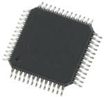
ICGOO电子元器件商城为您提供AD5391BSTZ-3由Analog设计生产,在icgoo商城现货销售,并且可以通过原厂、代理商等渠道进行代购。 AD5391BSTZ-3价格参考¥220.60-¥288.38。AnalogAD5391BSTZ-3封装/规格:数据采集 - 数模转换器, 12 位 数模转换器 16 52-LQFP(10x10)。您可以下载AD5391BSTZ-3参考资料、Datasheet数据手册功能说明书,资料中有AD5391BSTZ-3 详细功能的应用电路图电压和使用方法及教程。
AD5391BSTZ-3 是 Analog Devices Inc. 生产的一款数模转换器(DAC),具有双通道、12位分辨率、内置电压基准和轨到轨输出功能。它广泛应用于需要高精度模拟信号生成的场合。以下是其主要的应用场景:

1. 工业自动化与控制系统:用于过程控制中的设定值调节、传感器校准和执行器驱动,提供高精度和稳定性的模拟输出信号。

2. 测试与测量设备:如信号发生器、示波器和多用表,用于生成精确的参考信号或模拟传感器信号。

3. 通信系统:在无线基站和光通信设备中用于偏置电压调节、激光驱动器控制等。

4. 医疗设备:用于诊断设备中的信号调节、传感器激励和参数校准,满足对精度和稳定性的高要求。

5. 汽车电子:如发动机控制单元(ECU)、电池管理系统(BMS)中用于模拟信号调节和控制。

6. 消费电子与音频设备:用于高端音频设备中的音量控制和信号调节。

AD5391BSTZ-3 采用TSSOP封装,适合空间受限的应用,内置基准源简化了设计,适用于对精度和集成度要求较高的中低端信号生成场景。
| 参数 | 数值 |
| 产品目录 | 集成电路 (IC)半导体 |
| 描述 | IC DAC 12BIT 16CHAN 3V 52LQFP数模转换器- DAC 16-CH 12-Bit Vout IC |
| DevelopmentKit | EVAL-AD5391EBZ |
| 产品分类 | |
| 品牌 | Analog Devices Inc |
| 产品手册 | |
| 产品图片 |
|
| rohs | 符合RoHS无铅 / 符合限制有害物质指令(RoHS)规范要求 |
| 产品系列 | 数据转换器IC,数模转换器- DAC,Analog Devices AD5391BSTZ-3- |
| 数据手册 | |
| 产品型号 | AD5391BSTZ-3 |
| PCN设计/规格 | |
| 产品培训模块 | http://www.digikey.cn/PTM/IndividualPTM.page?site=cn&lang=zhs&ptm=19145http://www.digikey.cn/PTM/IndividualPTM.page?site=cn&lang=zhs&ptm=18614http://www.digikey.cn/PTM/IndividualPTM.page?site=cn&lang=zhs&ptm=26125http://www.digikey.cn/PTM/IndividualPTM.page?site=cn&lang=zhs&ptm=26140http://www.digikey.cn/PTM/IndividualPTM.page?site=cn&lang=zhs&ptm=26150http://www.digikey.cn/PTM/IndividualPTM.page?site=cn&lang=zhs&ptm=26147 |
| 产品种类 | 数模转换器- DAC |
| 位数 | 12 |
| 供应商器件封装 | 52-LQFP(10x10) |
| 其它名称 | AD5391BSTZ3 |
| 分辨率 | 12 bit |
| 包装 | 托盘 |
| 商标 | Analog Devices |
| 安装类型 | 表面贴装 |
| 安装风格 | SMD/SMT |
| 封装 | Tray |
| 封装/外壳 | 52-LQFP |
| 封装/箱体 | LQFP-52 |
| 工作温度 | -40°C ~ 85°C |
| 工厂包装数量 | 160 |
| 建立时间 | 8µs |
| 接口类型 | SPI |
| 数据接口 | I²C |
| 最大工作温度 | + 85 C |
| 最小工作温度 | - 40 C |
| 标准包装 | 1 |
| 电压参考 | Internal, External |
| 电压源 | 单电源 |
| 电源电压-最大 | 5.5 V |
| 电源电压-最小 | 2.7 V |
| 积分非线性 | +/- 1 LSB |
| 稳定时间 | 6 us |
| 系列 | AD5391 |
| 结构 | Resistor String |
| 设计资源 | |
| 转换器数 | 16 |
| 转换器数量 | 16 |
| 输出数和类型 | 16 电压,单极 |
| 输出类型 | Voltage |
| 配用 | /product-detail/zh/EVAL-AD5391EBZ/EVAL-AD5391EBZ-ND/1767480 |
| 采样比 | 167 kSPs |
| 采样率(每秒) | 167k |


- 商务部:美国ITC正式对集成电路等产品启动337调查
- 曝三星4nm工艺存在良率问题 高通将骁龙8 Gen1或转产台积电
- 太阳诱电将投资9.5亿元在常州建新厂生产MLCC 预计2023年完工
- 英特尔发布欧洲新工厂建设计划 深化IDM 2.0 战略
- 台积电先进制程称霸业界 有大客户加持明年业绩稳了
- 达到5530亿美元!SIA预计今年全球半导体销售额将创下新高
- 英特尔拟将自动驾驶子公司Mobileye上市 估值或超500亿美元
- 三星加码芯片和SET,合并消费电子和移动部门,撤换高东真等 CEO
- 三星电子宣布重大人事变动 还合并消费电子和移动部门
- 海关总署:前11个月进口集成电路产品价值2.52万亿元 增长14.8%


PDF Datasheet 数据手册内容提取
8-/16-Channel, 3 V/5 V, Serial Input, Single-Supply, 12-/14-Bit Voltage Output Data Sheet AD5390/AD5391/AD5392 FEATURES I2C-compatible interface Integrated functions AD5390: 16-channel, 14-bit voltage output DAC channel monitor AD5391: 16-channel, 12-bit voltage output DAC simultaneous output update via LDAC AD5392: 8-channel, 14-bit voltage output DAC clear function to user-programmable code Guaranteed monotonic amplifier boost mode to optimize slew rate INL user-programmable offset and gain adjust ±1 LSB max (AD5391) toggle mode enables square wave generation ±3 LSB max (AD5390-5/AD5392-5) thermal monitor ±4 LSB max (AD5390-3/AD5392-3) Robust 6.5 kV HBM and 2 kV FICDM ESD rating On-chip 1.25 V/2.5 V, 10 ppm/°C reference Temperature range: −40°C to +85°C APPLICATIONS Rail-to-rail output amplifier Instrumentation and industrial control Power-down mode Power amplifier control Package types Level setting (ATE) 64-lead LFCSP (9 mm × 9 mm) Control systems 52-lead LQFP (10 mm × 10 mm) Microelectromechanical systems (MEMs) User interfaces Variable optical attenuators (VOAs) Serial SPI-, QSPI-, MICROWIRE-, and DSP-compatible Optical transceivers (MSA 300, XFP) (featuring data readback) FUNCTIONAL BLOCK DIAGRAM DVDD (×3) DGND (×3/×4) AVDD(×2) AGND (×2) DAC_GND (×2) REF_GND REFOUT/REFINSIGNAL_GND (×2) 1.25V/2.5V AD5390 REFERENCE SPI/I2C 14 INPUT 14 14 DAC 14 REG REG DAC 0 DCEN/AD1 0 0 VOUT 0 14 m REG0 SCDLINK//SSDCAL INTERFACE MSATCAHTINEE 14 c REG0 R R CONTROL AND SYNC/AD0 LOGIC CONTROL 14 INPUT 14 14 DAC 14 SDO LOGIC REG REG DAC 1 1 1 VOUT 1 14 m REG1 VOUT 2 14 c REG1 R R VOUT 3 BUSY VOUT 4 PD 14 INPUT 14 14 DAC 14 VOUT 5 REG REG DAC 6 CLR 6 6 VOUT 6 RESET PORWEESRE-TON 14 m REG6 14 c REG6 R R VIN0 VIN15 14 INPUT 14 14 DAC 14 REG REG DAC 7 7 7 VOUT 7 MON_IN1 14 m REG7 VOUT 8 MON_IN2 MUX 14 c REG7 ×2 R R VOUT 15 MON_OUT LDAC 03773-001 Figure 1. Rev. F Document Feedback Information furnished by Analog Devices is believed to be accurate and reliable. However, no responsibility is assumed by Analog Devices for its use, nor for any infringements of patents or other One Technology Way, P.O. Box 9106, Norwood, MA 02062-9106, U.S.A. rights of third parties that may result from its use. Specifications subject to change without notice. No license is granted by implication or otherwise under any patent or patent rights of Analog Devices. Tel: 781.329.4700 ©2004–2014 Analog Devices, Inc. All rights reserved. Trademarks and registered trademarks are the property of their respective owners. Technical Support www.analog.com
AD5390/AD5391/AD5392 Data Sheet TABLE OF CONTENTS Features .............................................................................................. 1 I2C Write Operation ....................................................................... 28 Applications ....................................................................................... 1 4-Byte Mode ................................................................................ 28 Functional Block Diagram .............................................................. 1 3-Byte Mode ................................................................................ 29 Revision History ............................................................................... 3 2-Byte Mode ................................................................................ 30 General Description ......................................................................... 4 AD5390/AD5391/AD5392 On-Chip Special Function Specifications ..................................................................................... 5 Registers ....................................................................................... 31 AD5390-5/AD5391-5/AD5392-5 Specifications ..................... 5 Control Register Write ............................................................... 33 AD5390-5/AD5391-5/AD5392-5 AC Characteristics............. 7 Hardware Functions ....................................................................... 35 AD5390-3/AD5391-3/AD5392-3 Specifications ..................... 8 Reset Function ............................................................................ 35 AD5390-3/AD5391-3/AD5392-3 AC Characteristics........... 10 Asynchronous Clear Function .................................................. 35 Timing Characteristics ................................................................... 11 BUSY and LDAC Functions...................................................... 35 Serial SPI-, QSPI-, MICROWIRE-, and DSP-Compatible Power-On Reset .......................................................................... 35 Interface ....................................................................................... 11 Power-Down ............................................................................... 35 I2C Serial Interface ...................................................................... 13 Microprocessor Interfacing ....................................................... 35 Absolute Maximum Ratings .......................................................... 14 Application Information ................................................................ 37 ESD Caution ................................................................................ 14 Power Supply Decoupling ......................................................... 37 Pin Configuratons and Function Descriptions .......................... 15 Power Supply Sequencing ......................................................... 38 Terminology .................................................................................... 18 Typical Configuration Circuit .................................................. 39 Typical Performance Characteristics ........................................... 19 AD5390/AD5391/AD5392 Monitor Function ....................... 40 Functional Description .................................................................. 23 Toggle Mode Function ............................................................... 40 DAC Architecture ....................................................................... 23 Thermal Monitor Function ....................................................... 40 Data Decoding ............................................................................ 24 Outline Dimensions ....................................................................... 42 Interfaces .......................................................................................... 25 Ordering Guide .......................................................................... 43 DSP-, SPI-, and MICROWIRE-Compatible Serial Interface ...... 25 I2C Serial Interface ...................................................................... 27 Rev. F | Page 2 of 44
Data Sheet AD5390/AD5391/AD5392 REVISION HISTORY 6/14—Rev. E to Rev. F 1/09—Rev. B to Rev. C Deleted Table 1; Renumbered Sequentially ................................... 4 Updated Format ................................................................. Universal Changed AD5390-3/AD5391-3/AD5392-3 Input Current from Changes to Figure 33 ...................................................................... 27 ±10 µA (max) to ±1 µA (max); Table 3 .......................................... 8 Added Figure 34 and Renumbered Sequentially ........................ 27 Changes to Table 5 .......................................................................... 11 Changes to Figure 34 ...................................................................... 28 Changes to Soft Reset Section ....................................................... 31 Changes to Table 28 ........................................................................ 33 Changes to Reset Function Section .............................................. 35 Change order of Figure 41 and Figure 42 .................................... 36 Replaced ADSP2101 with ADSP-BF527 ...................................... 36 Changes to Toggle Mode Function Section ................................. 37 Added Power Supply Sequencing Section ................................... 38 3/06—Rev. A to Rev. B Changes to Ordering Guide ........................................................... 43 Changes to Figure 1 .......................................................................... 1 6/12—Rev. D to Rev. E Changes to Table 9 .......................................................................... 14 Changes to Table 1 ............................................................................ 4 Changes to Table 12 and Table 15 ................................................. 23 Change to Accuracy Parameter, Gain Error, Table 2 .................... 5 Updated Outline Dimensions........................................................ 39 Change to Accuracy Parameter, Gain Error, Table 4 .................... 8 Changes to Ordering Guide ........................................................... 40 Added Exposed Pad Notation to Figure 7 and Figure 8 ............ 15 10/04—Rev. 0 to Rev. A 5/12—Rev. C to Rev. D Changes to Features .......................................................................... 1 Changes to Product Title and Features Section ............................ 1 Changes to Table 1 ............................................................................ 3 Changes to Table 2 ............................................................................ 4 Changes to Table 2 ............................................................................ 4 Changes to Table 3 ............................................................................ 6 Changes to Table 3 ............................................................................ 6 Changes to Table 4 ............................................................................ 7 Changes to Table 4 ............................................................................ 7 Changes to Table 5 ............................................................................ 9 Changes to Figure 36 ...................................................................... 35 Changes to Table 6 .......................................................................... 10 Changes to Figure 37 ...................................................................... 36 Changes to Table 8 .......................................................................... 13 Changes to Figure 38 ...................................................................... 36 Changes to Figure 8 and Figure 10 ............................................... 14 Changes to Ordering Guide ........................................................... 41 Changes to Table 9 .......................................................................... 16 4/04—Revision 0: Initial Version Changes to Figure 17, Figure 18, Figure 19, And Figure 22 ...... 19 Changes to Figure 23, Figure 24, Figure 25, and Figure 26 ....... 20 Changes to Table 26 ........................................................................ 32 Changes to Ordering Guide ........................................................... 40 Rev. F | Page 3 of 44
AD5390/AD5391/AD5392 Data Sheet GENERAL DESCRIPTION The AD5390/AD5391 are complete single-supply, 16-channel, The AD5390/AD5391/AD5392 contain a 3-wire serial interface 14-bit and 12-bit DACs, respectively. The AD5392 is a complete with interface speeds in excess of 30 MHz that are compatible single-supply, 8-channel, 14-bit DAC. The devices are available with SPI®, QSPI™, MICROWIRE™, and DSP interface standards in either a 64-lead LFCSP or a 52-lead LQFP. All channels have and an I2C-compatible interface supporting a 400 kHz data an on-chip output amplifier with rail-to-rail operation. All transfer rate. devices include an internal 1.25/2.5 V, 10 ppm/°C reference, an An input register followed by a DAC register provides double- on-chip channel monitor function that multiplexes the analog buffering, allowing DAC outputs to be updated independently outputs to a common MON_OUT pin for external monitoring, or simultaneously using the LDAC input. Each channel has a and an output amplifier boost mode that optimizes the output programmable gain and offset adjust register, letting the user amplifier slew rate. fully calibrate any DAC channel. Power consumption is typically 0.25 mA per channel. Rev. F | Page 4 of 44
Data Sheet AD5390/AD5391/AD5392 SPECIFICATIONS AD5390-5/AD5391-5/AD5392-5 SPECIFICATIONS AV = 4.5 V to 5.5 V; DV = 2.7 V to 5.5 V; AGND = DGND = 0 V; REFIN = 2.5 V external. All specifications T to T , DD DD MIN MAX unless otherwise noted. Table 1. AD5390-51 Parameter AD5392-51 AD5391-51 Unit Test Conditions/Comments ACCURACY Resolution 14 12 Bits Relative Accuracy ±3 ±1 LSB max Differential Nonlinearity −1/+2 ±1 LSB max Guaranteed monotonic over temperature Zero-Scale Error 4 4 mV max Offset Error ±4 ±4 mV max Measured at Code 32 in the linear region (AD5390-5/AD5391-5); measured at Code 8 in the linear region (AD5391-5) Offset Error TC ±5 ±5 µV/°C typ Gain Error ±0.05 ±0.05 % FSR max At 25°C T to T MIN MAX ±0.06 ±0.06 % FSR max Gain Temperature Coefficient2 2 2 ppm FSR/°C typ DC Crosstalk2 1 1 LSB max REFERENCE INPUT/OUTPUT Reference Input2 Reference Input Voltage 2.5 2.5 V ±1% for specified performance, AV = 2 × REFIN + 50 mV DD DC Input Impedance 1 1 MΩ min Typically 100 MΩ Input Current ±1 ±1 µA max Typically ±30 nA Reference Range 1 V to AV /2 1 V to AV /2 V min/max DD DD Reference Output3 Enabled via internal/external bit in control register; REF select bit in control register selects the reference voltage Output Voltage 2.495/2.505 2.495/2.505 V min/max At ambient, optimized for 2.5 V operation 1.22/1.28 1.22/1.28 V min/max At ambient when 1.25 V reference is selected Reference TC ±10 ±10 ppm max Temperature range: 25°C to 85°C ±15 ±15 ppm max Temperature range: −40°C to +85°C Output Impedance 800 800 Ω typ OUTPUT CHARACTERISTICS2 Output Voltage Range4 0/AV 0/AV V min/max DD DD Short-Circuit Current 40 40 mA max Load Current ±1 ±1 mA max Capacitive Load Stability R = ∞ 200 200 pF max L R = 5 kΩ 1000 1000 pF max L DC Output Impedance 0.6 0.6 Ω max MONITOR OUTPUT PIN Output Impedance 1000 1000 Ω typ Three-State Leakage Current 100 100 nA typ LOGIC INPUTS2 DV = 2.7 V to 5.5 V DD V , Input High Voltage 2 2 V min IH V , Input Low Voltage IL DVDD > 3.6 V 0.8 0.8 V max DVDD ≤ 3.6 V 0.6 0.6 V max Input Current ±10 ±10 µA max Total for all pins, T = T to T A MIN MAX Pin Capacitance 10 10 pF max Rev. F | Page 5 of 44
AD5390/AD5391/AD5392 Data Sheet AD5390-51 Parameter AD5392-51 AD5391-51 Unit Test Conditions/Comments LOGIC INPUTS (SCL, SDA Only) V , Input High Voltage 0.7 × DV 0.7 × DV V min SMBus-compatible at DV < 3.6 V IH DD DD DD V , Input Low Voltage 0.3 × DV 0.3 × DV V max SMBus-compatible at DV < 3.6 V IL DD DD DD I , Input Leakage Current ±1 ±1 µA max IN V , Input Hysteresis 0.05 × DV 0.05 × DV V min HYST DD DD C , Input Capacitance 8 8 pF typ IN Glitch Rejection 50 50 ns max Input filtering suppresses noise spikes of <50 ns LOGIC OUTPUTS (BUSY, SDO)2 Output Low Voltage 0.4 0.4 V max DV = 5 V ± 10%, sinking 200 µA DD Output High Voltage DV − 1 DV − 1 V min DV = 5 V ± 10%, SDO only, sourcing 200 µA DD DD DD Output Low Voltage 0.4 0.4 V max DV = 2.7 V to 3.6 V, sinking 200 µA DD Output High Voltage DV − 0.5 DV − 0.5 V min DV = 2.7 V to 3.6 V SDO only, sourcing 200 µA DD DD DD High Impedance Leakage Current ±1 ±1 µA max High Impedance Output Capacitance 5 5 pF typ LOGIC OUTPUT (SDA)2 V , Output Low Voltage 0.4 0.4 V max I = 3 mA OL SINK 0.6 0.6 V max I = 6 mA SINK Three-State Leakage Current ±1 ±1 µA max Three-State Output Capacitance 8 8 pF typ POWER REQUIREMENTS AV 4.5/5.5 4.5/5.5 V min/max DD DV 2.7/5.5 2.7/5.5 V min/max DD Power Supply Sensitivity2 ∆Midscale/∆AV −85 −85 dB typ DD AI 0.375 0.375 mA/channel Outputs unloaded, boost off, DD max 0.25 mA/channel typ AI 0.475 0.475 mA/channel Outputs unloaded, boost on, DD max 0.325 mA/channel typ DI 1 1 mA max V = DV , V = DGND DD IH DD IL AI (Power-Down) 20 20 µA max Typically 100 nA DD DI (Power-Down) 20 20 µA max Typically 1 µA DD Power Dissipation 35 35 mW max AD5390/AD5391 with outputs unloaded, AV = DV = 5 V, boost off DD DD 20 20 mW max AD5392 with outputs unloaded, AV = DV = 5 V, boost off DD DD 1 The AD5390-5/AD5391-5/AD5392-5 are calibrated with a 2.5 V reference. Temperature range for all versions: −40°C to +85°C. 2 Guaranteed by characterization, not production tested. 3 Programmable either to 1.25 V typical or 2.5 V typical via the AD5390/AD5391/AD5392 control register. Operating the AD5390-5/AD5391-5/AD5392-5 with a reference of 1.25 V leads to a degradation in performance accuracy. 4 Accuracy guaranteed from VOUT = 10 mV to AVDD − 50 mV. Rev. F | Page 6 of 44
Data Sheet AD5390/AD5391/AD5392 AD5390-5/AD5391-5/AD5392-5 AC CHARACTERISTICS AV = 4.5 V to 5.5 V; DV = 2.7 V to 5.5 V; AGND = DGND = 0 V. DD DD Table 2. Parameter All1 Unit Test Conditions/Comments DYNAMIC PERFORMANCE Output Voltage Settling Time ¼ scale to ¾ scale change settling to ±1 LSB AD5390/AD5392 3 µs typ Boost mode off, CR11 = 0 8 µs max Boost mode off, CR11 = 0 AD5391 3 µs typ Boost mode off, CR11 = 0 8 µs max Boost mode off, CR11 = 0 Slew rate2 2.5 V/µs typ Boost mode on 1.5 V/µs typ Boost mode off Digital-to-Analog Glitch Energy 12 nV-s typ Glitch Impulse Peak Amplitude 15 mV typ Channel-to-Channel Isolation 100 dB typ See the Terminology section DAC-to-DAC Crosstalk 1 nV-s typ See the Terminology section Digital Crosstalk 0.8 nV-s typ Digital Feedthrough 0.1 nV-s typ Effect of input bus activity on DAC output under test Output Noise (0.1 Hz to 10 Hz) 15 µV p-p typ External reference midscale loaded to DAC 40 µV p-p typ Internal reference midscale loaded to DAC Output Noise Spectral Density @ 1 kHz 150 nV/(Hz)1/2 typ @ 10 kHz 100 nV/(Hz)1/2 typ 1 Guaranteed by characterization, not production tested. 2 The slew rate can be adjusted via the current boost control bit in the DAC control register. Rev. F | Page 7 of 44
AD5390/AD5391/AD5392 Data Sheet AD5390-3/AD5391-3/AD5392-3 SPECIFICATIONS AV = 2.7 V to 3.6 V; DV = 2.7 V to 5.5 V; AGND = DGND = 0 V; REFIN = 1.25 V external. All specifications T to T , DD DD MIN MAX unless otherwise noted. Table 3. AD5390-31 Parameter AD5392-31 AD5391-31 Unit Test Conditions/Comments ACCURACY Resolution 14 12 Bits Relative Accuracy ±4 ±1 LSB max Differential Nonlinearity −1/+2 ±1 LSB max Guaranteed monotonic over temperature Zero-Scale Error 4 4 mV max Offset Error ±4 ±4 mV max Measured at code 64 in the linear region Offset Error TC ±5 ±5 µV/°C typ Gain Error ±0.05 ±0.05 % FSR max At 25°C ±0.1 ±0.1 % FSR max T to T MIN MAX Gain Temperature Coefficient2 2 2 ppm FSR/°C typ DC Crosstalk 1 1 LSB max REFERENCE INPUT/OUTPUT Reference Input2 Reference Input Voltage 1.25 1.25 V ±1% for specified performance DC Input Impedance 1 1 MΩ min Typically 100 MΩ Input Current ±1 ±1 µA max Typically ±30 nA Reference Range 1 V to AV /2 1 V to AV /2 V min/max DD DD Reference Output3 Enabled via internal/external bit in control register; REF select bit in control register selects the reference voltage Output Voltage 1.245/1.255 1.245/1.255 V min/max At ambient, optimized for 1.25 V operation 2.47/2.53 2.47/2.53 V min/max At ambient when 2.5 V reference is selected Reference TC ±10 ±10 ppm max Temperature range: 25°C to 85°C ±15 ±15 ppm max Temperature range: −40°C to +85°C Output Impedance 800 800 Ω typ OUTPUT CHARACTERISTICS2 Output Voltage Range4 0/AV 0/AV V min/max DD DD Short-Circuit Current 40 40 mA max Load Current ±1 ±1 mA max Capacitive Load Stability R = ∞ 200 200 pF max L R = 5 kΩ 1000 1000 pF max L DC Output Impedance 0.6 0.6 Ω max MONITOR OUTPUT PIN2 Output Impedance 1000 1000 Ω typ Three-State Leakage Current 100 100 nA typ LOGIC INPUTS2 DV = 2.7 V to 5.5 V DD V , Input High Voltage 2 2 V min IH V , Input Low Voltage IL DVDD > 3.6 V 0.8 0.8 V max DVDD ≤ 3.6 V 0.6 0.6 V max Input Current ±1 ±1 µA max Total for all pins. T = T to T A MIN MAX Pin Capacitance 10 10 pF max Rev. F | Page 8 of 44
Data Sheet AD5390/AD5391/AD5392 AD5390-31 Parameter AD5392-31 AD5391-31 Unit Test Conditions/Comments Logic Inputs (SCL, SDA Only) V , Input High Voltage 0.7 × DV 0.7 × DV V min SMBus-compatible at DV < 3.6 V IH DD DD DD V , Input Low Voltage 0.3 × DV 0.3 × DV V max SMBus-compatible at DV < 3.6 V IL DD DD DD I , Input Leakage Current ±1 ±1 µA max IN V , Input Hysteresis 0.05 × DV 0.05 × DV V min HYST DD DD Glitch Rejection 50 50 ns max Input filtering suppresses noise spikes <50 ns Logic Outputs (BUSY, SDO)2 Output Low Voltage 0.4 0.4 V max DV = 2.7 V to 5.5 V, sinking 200 µA DD Output High Voltage DVDD − 0.5 DVDD − 0.5 V min DVDD = 2.7 V to 3.6 V, SDO only, sourcing 200 µA DVDD − 0.1 DVDD − 0.1 V min DVDD = 4.5 V to 5.5 V, SDO only, sourcing 200 µA High Impedance Leakage Current ±1 ±1 µA max High Impedance Output 5 5 pF typ Capacitance Logic Output (SDA)2 V , Output Low Voltage 0.4 0.4 V max I = 3 mA OL SINK 0.6 0.6 V max I = 6 mA SINK Three-State Leakage Current ±1 ±1 µA max Three-State Output 8 8 pF typ Capacitance POWER REQUIREMENTS AV 2.7/3.6 2.7/3.6 V min/max DD DV 2.7/5.5 2.7/5.5 V min/max DD Power Supply Sensitivity2 ∆Midscale/∆AV −85 −85 dB typ DD AI 0.375 0.375 mA/channel Outputs unloaded, boost off, DD max 0.25 mA/channel typ AI 0.475 0.475 mA/channel Outputs unloaded, boost on, DD max 0.325 mA/channel typ DI 1 1 mA max V = DV , V = DGND DD IH DD IL AI (Power-Down) 20 20 µA max Typically 100 nA DD DI (Power-Down) 20 20 µA max Typically 1 µA DD Power Dissipation 21 21 mW max AD5390/AD5391 with outputs unloaded, AV = DV = 3 V, boost off DD DD 12 12 mW max AD5392 with outputs unloaded, AV = DV = 3 V, boost off DD DD 1 The AD5390-3/AD5391-3/AD5392-3 are calibrated with a 1.25 V reference. Temperature range for all versions: −40°C to +85°C. 2 Guaranteed by characterization, not production tested. 3 Programmable either to 1.25 V typical or 2.5 V typical via the AD5390/AD5391/AD5392 control register. Operating the AD5390-3/AD5391-3/AD5392-3 with a reference of 2.5 V leads to a degradation in performance accuracy. 4 Accuracy guaranteed from VOUT = 39 mV to AVDD − 50 mV. Rev. F | Page 9 of 44
AD5390/AD5391/AD5392 Data Sheet AD5390-3/AD5391-3/AD5392-3 AC CHARACTERISTICS AV = 2.7 V to 3.6 V; DV = 2.7 V to 5.5 V; AGND = DGND = 0 V; C = 200 pF to AGND. DD DD L Table 4. Parameter All1 Unit Test Conditions/Comments DYNAMIC PERFORMANCE Output Voltage Settling Time ¼ scale to ¾ scale change settling to ±1 LSB AD5390/AD5392 3 µs typ Boost mode off, CR11 = 0 8 µs max Boost mode off, CR11 = 0 AD5391 3 µs typ Boost mode off, CR11 = 0 8 µs max Boost mode on, CR11 = 1 Slew Rate2 2.5 V/µs typ Boost mode on 1.5 V/µs typ Boost mode off, CR11 = 0 Digital-to-Analog Glitch Energy 12 nV-s typ Glitch Impulse Peak Amplitude 15 mV typ Channel-to-Channel Isolation 100 dB typ See the Terminology section DAC-to-DAC Crosstalk 1 nV-s typ See the Terminology section Digital Crosstalk 0.8 nV-s typ Digital Feedthrough 0.1 nV-s typ Effect of input bus activity on DAC output under test OUTPUT NOISE (0.1 Hz to 10 Hz) 15 µV p-p typ External reference midscale loaded to DAC 40 µV p-p typ Internal reference midscale loaded to DAC Output Noise Spectral Density @ 1 kHz 150 nV/(Hz)1/2 typ @ 10 kHz 100 nV/(Hz)1/2 typ 1 Guaranteed by design and characterization, not production tested. 2 The slew rate can be programmed via the current boost control bit in the AD5390/AD5391/AD5392 control registers. Rev. F | Page 10 of 44
Data Sheet AD5390/AD5391/AD5392 TIMING CHARACTERISTICS SERIAL SPI-, QSPI-, MICROWIRE-, AND DSP-COMPATIBLE INTERFACE DV = 2 V to 5.5 V; AV = 2.7 V to 5.5 V; AGND = DGND = 0 V. All specifications T to T , unless otherwise noted. DD DD MIN MAX Table 5. 3-Wire Serial Interface1 Parameter2, 3 Limit at T , T Unit Description MIN MAX t 33 ns min SCLK cycle time 1 t 13 ns min SCLK high time 2 t 13 ns min SCLK low time 3 t 13 ns min SYNC falling edge to SCLK falling edge setup time 4 t4 13 ns min 24th SCLK falling edge to SYNC falling edge 5 t4 33 ns min Minimum SYNC low time 6 t 10 ns min Minimum SYNC high time 7 t 140 ns min Minimum SYNC high time in readback mode 7 t 5 ns min Data setup time 8 t 4.5 ns min Data hold time 9 t 4 36 ns max 24th SCLK falling edge to BUSY falling edge 10 t 670 ns max BUSY pulse width low (single channel update) 11 t 4 20 ns min 24th SCLK falling edge to LDAC falling edge 12 t 20 ns min LDAC pulse width low 13 t 100/2000 ns BUSY rising edge to DAC output response time 14 min/max t 0 ns min BUSY rising edge to LDAC falling edge 15 t 100 ns min LDAC falling edge to DAC output response time 16 t 3 μs typ DAC output settling time, AD5390/AD5391/AD5392; boost mode off 17 t 20 ns min CLR pulse width low 18 t 40 μs max CLR pulse activation time 19 t 5 20 ns max SCLK rising edge to SDO valid 20 t 4 5 ns min SCLK falling edge to SYNC rising edge 21 t 4 8 ns min SYNC rising edge to SCLK rising edge 22 t 4 20 ns min SYNC rising edge to LDAC falling edge 23 1 Guaranteed by design and characterization, not production tested. 2 All input signals are specified with tr = tf = 5 ns (10% to 90% of VCC) and timed from a voltage level of 1.2 V. 3 See Figure 2, Figure 3, Figure 4, and Figure 5. 4 Standalone mode only. 5 Daisy-chain mode only. t1 SCLK 24 48 t7 t3 t2 t21 t22 SYNC t4 t8 t9 DIN DB23 DB0 DB23 DB0 INPUT WORD FOR DAC N INPUT WORD FOR DAC N+1 t20 SDO DB23 DB0 UNDEFINED INPUT WORD FOR DAC N t23 LDAC t13 03773-002 Figure 2. Serial Interface Timing Diagram (Daisy-Chain Mode) Rev. F | Page 11 of 44
AD5390/AD5391/AD5392 Data Sheet t1 SCLK 1 2 24 24 t3 t2 t4 t5 SYNC t7 t6 t8 t9 DIN DB23 DB0 t10 BUSY t11 t12 t13 LDAC1 t17 VOUT 1 t14 t15 LDAC2 t13 t17 t16 VOUT 2 t18 CLR t19 VOUT 12LLDDAACC AACCTTIIVVEE DDUURRIINNGG BBUUSSYY 03773-005 Figure 3. Serial Interface Timing Diagram (Standalone Mode) SCLK 24 48 t7A SYNC DIN DB23 DB0 DB23' DB0 INPUT WORD SPECIFIES NOP CONDITION REGISTER TO BE READ SDO DB23 DB0 UNDEFINED SELECCTLEODC RKEEGDI SOTUETR DATA 03773-006 Figure 4. Serial Interface Timing Diagram (Data Readback Mode) 200µA IOL TO VOH (MIN) OR OUTPPUINT CL VOL (MAX) 50pF 200µA IOH 03773-003 Figure 5. Load Circuit for Digital Output Timing Rev. F | Page 12 of 44
Data Sheet AD5390/AD5391/AD5392 I2C SERIAL INTERFACE DV = 2.7 V to 5.5 V; AV = 2.7 V to 5.5 V; AGND = DGND = 0 V. All specifications T to T , unless otherwise noted. DD DD MIN MAX Table 6. I2C Serial Interface1 Parameter2 Limit at T , T Unit Description MIN MAX F 400 kHz max SCL clock frequency SCL t 2.5 μs min SCL cycle time 1 t 0.6 μs min t , SCL high time 2 HIGH t 1.3 μs min t , SCL low time 3 LOW t 0.6 μs min t , , start/repeated start condition hold time 4 HD STA t 100 ns min t , , data setup time 5 SU DAT t3 0.9 μs max t , data hold time 6 HD DAT 0 μs min t , data hold time HD DAT t 0.6 μs min t , setup time for repeated start 7 SU STA t 0.6 μs min t , stop condition setup time 8 SU STO t 1.3 μs min t , bus free time between a stop and a start condition 9 BUF t 300 ns max t, fall time of SDA when transmitting 10 F 0 ns min t, rise time of SCL and SDA when receiving (CMOS-compatible) R t 300 ns max t, fall time of SDA when transmitting 11 F 0 ns min t, fall time of SDA when receiving (CMOS-compatible) F 300 ns max t, fall time of SCL and SDA when receiving F 20 + 0.1 C ns min t, fall time of SCL and SDA when transmitting B F C4 400 pF max Capacitive load for each bus line B 1 Guaranteed by design and characterization, not production tested. 2 See Figure 6. 3 A master device must provide a hold time of at least 300 ns for the SDA signal (referred to the VIH MIN of the SCL signal) to bridge the undefined region of SCL’s falling edge. 4 CB is the total capacitance of one bus line in pF; tR and tF measured between 0.3 DVDD and 0.7 DVDD. SDA t9 t3 t10 t11 t4 SCL t4 t6 t2 t5 t7 t1 t8 COSNTDAIRTITON CROESPNTEDAAIRTTITEODN COSNTDOITPION 03773-007 Figure 6. I2C Interface Timing Diagram Rev. F | Page 13 of 44
AD5390/AD5391/AD5392 Data Sheet ABSOLUTE MAXIMUM RATINGS Transient currents of up to 100 mA do not cause SCR latch-up. T = 25°C, unless otherwise noted. A Stresses above absolute maximum ratings may cause permanent damage to the device. This is a stress rating only; functional Table 7. operation of the device at these or any other conditions above Parameter Rating those listed in the operational sections of this specification is AV to AGND −0.3 V to +7 V DD not implied. Exposure to absolute maximum rating conditions DV to DGND −0.3 V to +7 V DD for extended periods may affect device reliability. Digital Inputs to DGND −0.3 V to DV + 0.3 V DD Digital Outputs to DGND −0.3 V to DV + 0.3 V ESD CAUTION DD VREF to AGND −0.3 V to +7 V REFOUT to AGND −0.3 V to +7 V AGND to DGND −0.3 V to +0.3 V VOUTX to AGND −0.3 V to AV + 0.3 V DD ESD HBM 6.5 kV FICSM 2 kV Operating Temperature Range Commercial (B Version) −40°C to +85°C Storage Temperature Range −65°C to +150°C Junction Temperature (T max) 150°C J 64-Lead LFCSP, θ 22°C/W JA 52-Lead LQFP, θ 38°C/W JA Reflow Soldering Peak Temperature 230°C Rev. F | Page 14 of 44
Data Sheet AD5390/AD5391/AD5392 PIN CONFIGURATONS AND FUNCTION DESCRIPTIONS CLRDGNDSYNC/AD0DIN/SDASCLK/SCLSDODVDDDGNDDGNDDVDDDVDDDGND2SPI/ICPDDCEN/AD1LDAC DGNDSYNC/AD0DIN/SDASCLK/SCLSDODVDDDGNDDVDDDVDDDGND2CSPI/IPDDCEN/AD1 4321098765432109 52 51 50 49 48 47 46 45 44 43 42 41 40 6666655555555554 CLR 1 39 LDAC NC 2 38 BUSY NC 1 48 NC PIN 1 NC 2 47 BUSY NC 3 INDICATOR 37 RESET NC 3 PIN 1 46 RESET REF_GND 4 36 NC NNCC 45 INDICATOR 4445 NNCC REFOUT/REFIN 5 AD5390/ 35 NC NC 6 43 NC SIGNAL_GND 1 6 34 NC REF_GND 7 AD5390/ 42 NC DAC_GND 1 7 AD5391 33 NC SRIEGFNOAULT_/GRENFDI N1 89 AD5391 4410 NNCC AVDD 1 8 (NToOt Pto V SIEcaWle) 32 AVDD2 DAC_GND 110 TOP VIEW 39 NC VOUT 0 9 31 AGND 2 VAOVUDDT 101112 (Not to Scale) 3378 ANVCDD2 VOUT 110 30 VOUT 15 VOUT 113 36 AGND 2 VOUT 211 29 VOUT 14 VOUT 214 35 VOUT 15 VOUT 312 28 VOUT 13 VOUT 315 34 VOUT 14 VOUT 416 33 VOUT 13 VOUT 413 27 SIGNAL_GND 2 1415 16 17 18 19 20 21 22 23 24 25 26 AGND 1 17NC 18NC 19VOUT 5 20VOUT 6 21VOUT 7 22MON_IN 1 23MON_IN 2 24MON_OUT 25VOUT 8 26VOUT 9 27VOUT 10 28VOUT 11 29VOUT 12 30AC_GND 2 31AL_GND 2 32 NC = NO CONNECT AGND 1VOUT 5VOUT 6VOUT 7MON_IN 1MON_IN 2MON_OUTVOUT 8VOUT 9VOUT 10VOUT 11VOUT 12DAC_GND 2 03773-010 DN G N12..O NTTHCEE S= ENXOP OCOSENDN EPCATD. SHOULD BE CONNECTED TO THESI GROUND PLANE. 03773-008 Figure 7. AD5390/AD5391 LFCSP Pin Configuration Figure 9. AD5390/AD5391 LQFP Pin Configuration CLRDGNDSYNC/AD0DIN/SDASCLK/SCLSDODVDDDGNDDGNDDVDDDVDDDGND2SPI/ICPDDCEN/AD1LDAC DGNDSYNC/AD0DIN/SDASCLK/SCLSDODVDDDGNDDVDDDVDDDGND2CSPI/IPDDCEN/AD1 64636261605958575655545352515049 52 51 50 49 48 47 46 45 44 43 42 41 40 CLR 1 39 LDAC NC 1 48 NC NC 2 PIN 1 38 BUSY NC 2 47 BUSY NC 3 INDICATOR 37 RESET NNCC 34 PININD I1CATOR 4456 RNECSET REF_GND 4 36 NC NC 5 44 NC REFOUT/REFIN 5 35 NC NC 6 43 NC SIGNAL_GND 1 6 AD5392 34 NC REF_GND 7 42 NC REFOUT/REFIN 8 AD5392 41 NC DAC_GND 1 7 TOP VIEW 33 NC SIGNAL_GND 1 9 TOP VIEW 40 NC AVDD 1 8 (Not to Scale) 32 NC DAC_AGVNDDD 111101 (Not to Scale) 3398 NNCC VOUT 0 9 31 NC VOUT 012 37 NC VOUT 110 30 NC VVOOUUTT 121134 3356 NNCC VOUT 211 29 NC VOUT 315 34 NC VOUT 312 28 NC VOUT 416 33 NC VOUT 413 27 SIGNAL_GND 2 1415 16 17 18 19 20 21 22 23 24 25 26 AGND 1 17NC 18NC 19VOUT 5 20VOUT 6 21VOUT 7 22MON_IN 1 23MON_IN 2 24MON_OUT 25TEST 26NC 27NC 28NC 29NC 30AC_GND 2 31AL_GND 2 32 NC = NO CONNECT AGND 1VOUT 5VOUT 6VOUT 7MON_IN 1MON_IN 2MON_OUTTESTNC NC NC NCDAC_GND 2 03773-011 DN G N12..O NTTHCEE S= ENXOP OCOSENDN EPCATD. SHOULD BE CONNECTED TO THE GSIROUND PLANE. 03773-009 Figure 8. AD5392 LFCSP Pin Configuration Figure 10. AD5392 LQFP Pin Configuration Rev. F | Page 15 of 44
AD5390/AD5391/AD5392 Data Sheet Table 8. Pin Function Descriptions Mnemonic Function VOUT X Buffered Analog Outputs for Channel X. Each analog output is driven by a rail-to-rail output amplifier operating at a gain of 2. Each output is capable of driving an output load of 5 kΩ to ground. Typical output impedance is 0.5 Ω. SIGNAL_GND 1, Analog Ground Reference Points for each group of eight output channels. All SIGNAL_GND pins are tied together SIGNAL_GND 2 internally and should be connected to the AGND plane as close as possible to the AD5390/AD5391/AD5392. DAC_GND 1, Each group of eight channels contains a DAC_GND pin. This is the ground reference point for the internal 14-bit DACs. DAC_GND 2 These pins should be connected to the AGND plane. AGND 1, AGND 2 Analog Ground Reference Point. Each group of eight channels contains an AGND pin. All AGND pins should be connected externally to the AGND plane. AV 1, AV 2 Analog Supply Pins. Each group of eight channels has a separate AV pin. These pins should be decoupled with 0.1 uF DD DD DD ceramic capacitors and 10 µF tantalum capacitors. Operating range is 5 V ± 10%. DGND Ground for All Digital Circuitry. DV Logic Power Supply. Guaranteed operating range is 2.7 V to 5.5 V. Recommended that these pins be decoupled with DD 0.1 µF ceramic capacitors and 10 µF tantalum capacitors to DGND. REF_GND Ground Reference Point for the Internal Reference. Connect to AGND. REFOUT/REFIN The AD5390/AD5391/AD5392 contains a common REFOUT/REFIN pin. When the internal reference is selected, this pin is the reference output. If the application necessitates the use of an external reference, it can be applied to this pin and the internal reference disabled via the control register. The default for this pin is a reference input. MON_OUT Analog Output Pin. When the monitor function is enabled on the AD5390/AD5391, the MON_OUT acts as the output of a 16-to-1 channel multiplexer that can be programmed to multiplex any channel output to the MON_OUT pin. When the monitor function is enabled on the AD5392, the MON_OUT acts as the output of an 8-to-1 channel multiplexer that can be programmed to multiplex any channel output to the MON_OUT pin. The MON_OUT pin output impedance is typically 500 Ω and is intended to drive a high input impedance such as that exhibited by SAR ADC inputs. MON_IN 1, Monitor Input Pins. The AD5390/AD5391/AD5392 contains two monitor input pins to which the user can connect input MON_IN 2 signals (within the maximum ratings of the device) for monitoring purposes. Any of the signals applied to the MON_IN pins along with the output channels can be switched to the MON_OUT pin via software. An external ADC, for example, can be used to monitor these signals. SYNC/AD0 Serial Interface Pin. This is the frame synchronization input signal for the serial interface. When taken low, the internal counter is enabled to count the required number of clocks before the addressed register is updated. In I2C mode, AD0 acts as a hardware address pin. DCEN/AD1 Interface Control Pin. Operation is determined by the interface select bit SPI/I2C. Serial Interface Mode: Daisy-Chain Select Input (level-sensitive, active high). When high, this pin enables daisy-chain operation to allow a number of devices to be cascaded together. I2C Mode: This pin acts as a hardware address pin used in conjunction with AD0 to determine the software address for this device on the I2C bus. SDO Serial Data Output. Three-state CMOS output. SDO can be used for daisy-chaining a number of devices together. Data is clocked out on SDO on the rising edge of SCLK and is valid on the falling edge of SCLK. BUSY Digital CMOS Output. BUSY goes low during internal calculations of the data (x2) loaded to the DAC data register. During this time, the user can continue writing new data to further the x1, c, and m registers (these are stored in a FIFO), but no further updates to the DAC registers and DAC outputs can take place. If LDAC is taken low while BUSY is low, this event is stored. BUSY also goes low during power-on reset and when the RESET pin is low. During this time the interface is disabled and any events on LDAC are ignored. A CLR operation also brings BUSY low. LDAC Load DAC Logic Input (active low). If LDAC is taken low while BUSY is inactive (high), the contents of the input registers are transferred to the DAC registers and the DAC outputs are updated. If LDAC is taken low while BUSY is active and internal calculations are taking place, the LDAC event is stored and the DAC registers are updated when BUSY goes inactive. However, any events on LDAC during power-on reset or RESET are ignored. CLR Asynchronous Clear Input. The CLR input is falling edge sensitive. While CLR is low, all LDAC pulses are ignored. When CLR is activated, all channels are updated with the data contained in the CLR code register. BUSY is low for a duration of 20 µs (AD5390/AD5391) and 15 µs (AD5392) while all channels are being updated with the CLR code. RESET Asynchronous Digital Reset Input (falling edge sensitive). The function of this pin is equivalent to that of the power-on reset generator. When this pin is taken low, the state machine initiates a reset sequence to digitally reset the x1, m, c, and x2 registers to their default power-on values. This sequence takes 270 µs maximum. This falling edge of RESET initiates the RESET process and BUSY goes low for the duration, returning high when RESET is complete. While BUSY is low, all interfaces are disabled and all LDAC pulses are ignored. When BUSY returns high, the part resumes normal operation and the status of the RESET pin is ignored until the next falling edge is detected. Rev. F | Page 16 of 44
Data Sheet AD5390/AD5391/AD5392 Mnemonic Function PD Power-Down (level-sensitive, active high). Used to place the device in low power mode, in which the device consumes 1 µA analog current and 20 µA digital current. In power-down mode, all internal analog circuitry is placed in low power mode; the analog output is configured as high impedance outputs or provides a 100 kΩ load to ground, depending on how the power-down mode is configured. The serial interface remains active during power-down. SPI/I2C Interface Select Input Pin. When this input is low, I2C mode is selected. When this input is high, SPI mode is selected. SCLK/SCL Interface Clock Input Pin. In SPI-compatible serial interface mode, this pin acts as a serial clock input. It operates at clock speeds up to 50 MHz. I2C mode: In I2C mode, this pin performs the SCL function, clocking data into the device. Data transfer rate in I2C mode is compatible with both 100 kHz and 400 kHz operating modes. DIN/SDA Interface Data Input Pin. SPI/I2C = 1: This pin acts as the serial data input. Data must be valid on the falling edge of SCLK. SPI/I2C = 0, I2C mode: In I2C mode, this pin is the serial data pin (SDA) operating as an open drain input/output. TEST Test pin (AD5392 only). This pin is used for production testing. For normal operation, this pin should not be connected. NC No Connect. These pins have no internal connection. Exposed Pad This pad should be connected to the ground plane. (LFCSP only) Rev. F | Page 17 of 44
AD5390/AD5391/AD5392 Data Sheet TERMINOLOGY Relative Accuracy or Endpoint Linearity (INL) DC Output Impedance A measure of the maximum deviation from a straight line The effective output source resistance. It is dominated by passing through the endpoints of the DAC transfer function. package lead resistance. It is measured after adjusting for zero-scale error and full-scale Output Voltage Settling Time error and is expressed in least significant bits (LSBs). The amount of time it takes for the output of a DAC to settle Differential Nonlinearity (DNL) to a specified level for a ¼ to ¾ full-scale input change. It is The difference between the measured change and the ideal measured from the rising edge of BUSY. 1 LSB change between any two adjacent codes. A specified Digital-to-Analog Glitch Energy differential nonlinearity of 1 LSB maximum ensures mono- The amount of energy injected into the analog output at the tonicity. major code transition. It is specified as the area of the glitch in Zero-Scale Error nV-s. It is measured by toggling the DAC register data between The error in the DAC output voltage when all 0s are loaded 0x1FFF and 0x2000. into the DAC register. Ideally, with all 0s loaded to the DAC DAC-to-DAC Crosstalk and m = all 1s, c = 2n−1, VOUT = 0 V. (Zero-Scale) The glitch impulse that appears at the output of one DAC due to Zero-scale error is a measure of the difference between VOUT both the digital change and subsequent analog output change at (actual) and VOUT (ideal) expressed in mV. It is mainly caused another DAC. The victim channel is loaded with midscale, and by offsets in the output amplifier. DAC-to-DAC crosstalk is specified in nV-s. Offset Error Digital Crosstalk A measure of the difference between VOUT (actual) and VOUT The glitch impulse transferred to the output of one converter (ideal) expressed in mV in the linear region of the transfer due to a change in the DAC register code of another converter function. Offset error is measured on the AD5390-5/AD5391-5/ is defined as the digital crosstalk and is specified in nV-s. AD5392-5 with code 32 loaded in the DAC register and with Digital Feedthrough code 64 loaded in the DAC register on the AD5390-3/AD5391-3/ When the device is not selected, high frequency logic activity AD5392-3. on the device’s digital inputs can be capacitively coupled both Gain Error across and through the device to show up as noise on the VOUT The deviation in slope of the DAC transfer characteristic from pins. It can also be coupled along the supply and ground lines. ideal and is expressed in % FSR with the DAC output unloaded. This noise is digital feedthrough. Gain error is specified in the linear region of the output range Output Noise Spectral Density between VOUT = 10 mV and VOUT = AV − 50 mV. DD This is a measure of internally generated random noise. Random DC Crosstalk noise is characterized as a spectral density (voltage per √Hz). The dc change in the output level of one DAC at midscale in It is measured by loading all DACs to midscale and measuring response to a full-scale code (all 0s to all 1s and vice versa) and noise at the output. It is measured in nV/(Hz)1/2 in a 1 Hz the output change of all other DACs. It is expressed in LSBs. bandwidth at 10 kHz. Rev. F | Page 18 of 44
Data Sheet AD5390/AD5391/AD5392 TYPICAL PERFORMANCE CHARACTERISTICS 2.0 1.00 AVDD = DVDD = 5.5V VREF = 2.5V 1.5 TA = 25°C 0.75 1.0 0.50 B) 0.5 SB) 0.25 S L OR (L 0 ROR ( 0 R R R E L E –0.5 NL –0.25 N I I –1.0 –0.50 ––21..050 4096 INPU8T1 9C2ODE 12288 16384 03773-040 ––01..70500 512 1024 153I6NPU2T0 4C8ODE2560 3072 3584 409603773-043 Figure 11. AD5390-5/AD5392-5 Typical INL Plot Figure 14. Typical AD5391-5 INL Plot 2.0 1.00 AVDD = DVDD = 3V VREF = 1.25V 1.5 TA = 25°C 0.75 1.0 0.50 B) 0.5 SB) 0.25 S L OR (L 0 ROR ( 0 R R R E L E –0.5 NL –0.25 N I I –1.0 –0.50 ––21..050 4096 INPU8T1 9C2ODE 12288 16384 03773-041 ––01..70500 512 1024 153I6NPU2T0 4C8ODE2560 3072 3584 409603773-044 Figure 12. AD5390-3/AD5392-3 INL Plot Figure 15. Typical AD5391-3 INL Plot 40 14 AVDD = 5.5V RAEVFDDO U= T5 V= 2.5V REFIN = 2.5V 35 TEMP. RANGE = 25°C TO 85°C 12 TA = 25°C SAMPLE SIZE = 162 30 S10 NIT Y 25 U C R OF 8 QUEN 20 MBE 6 FRE 15 U N 4 10 20 –2 INL– 1ERROR DIST0RIBUTION (L1SB) 2 03773-042 05–5.0–4.5–4.0–3.5–3.0–2.5–R2.E0–F1E.5–R1E.0–N0C.5E0 D0R.5IF1T.0 (1p.p5m2.0/°2C.5)3.03.54.04.55.0 03773-045 Figure 13. AD5390/AD5392 INL Histogram Plot Figure 16. AD5390/AD5391/AD5392 REFOUT Temperature Coefficient Rev. F | Page 19 of 44
AD5390/AD5391/AD5392 Data Sheet 6 FULL SCALE 5 BUSY AVDD = DVDD= 5V 3/4 SCALE VREF = 2.5V 4 TA = 25°C V) 3 MIDSCALE T ( U O 2 V 1/4 SCALE VOUT 1 ZERO SCALE AVRVEDDF == D2.V5DVD = 5V 0 TA = 25°C 03773-100 –1–40 –20 –10 –5 C–U2RREN0T (mA2) 5 10 20 40 03773-049 Figure 17. AD5390/AD5391/AD5392 Exiting Soft Power-Down Figure 20. AD5390-5/AD5391-5/AD5392-5 Source and Sink Capability 0.20 AVDD = 5V VREF = 2.5V 0.15 TA = 25°C PD 0.10 V) ERROR AT ZERO SINKING CURRENT E ( 0.05 G A LT 0 O V R O–0.05 R R VOUT E–0.10 (VDD–VOUT) AT FULL-SCALE SOURCING CURRENT AVDD = DVDD = 5V VREF = 2.5V –0.15 TA = 25°C 03773-101 –0.200 0.25 0.50 0IS.7O5URCE1/I.S0I0NK (m1A.2)5 1.50 1.75 2.00 03773-050 Figure 18. AD5390/AD5391/AD5392 Exiting Hardware Power-Down Figure 21. Headroom at Rails vs. Source/Sink Current 2.510 AVDD = DVDD = 5V VREF = 2.5V TA = 25°C 2.505 VDD V) E ( G A2.500 T L O V VOUT 2.995 03773-102 2.9900 2 4 TIME6 (µs) 8 10 12 03773-103 Figure 19. AD5390/AD5391/AD5392 Power-Up Transient Figure 22. AD5390-5/AD5391-5/AD5392-5 Glitch Impulse Energy Rev. F | Page 20 of 44
Data Sheet AD5390/AD5391/AD5392 1.260 DVDD = 5.5V VIH = DVDD 10 VIL = DGND 1.255 TA = 25°C 8 V) S TAGE (1.250 F UNIT 6 L O VO ER B M 4 U 1.245 N 2 1.240 0 2 4 TIME6 (µs) 8 10 12 03773-104 0 0.5 0.6 0D.I7DD (mA)0.8 0.9 1.0 03773-107 Figure 23. AD5390-3/AD5391-3/AD5392-3 Glitch Impulse Figure 26. AD5390/AD5391/AD5392 DIDD Histogram 2.456 AVDD = DVDD = 5V VREF = 2.5V LDAC 2.455 TA = 25°C 14ns/SAMPLE NUMBER 2.454 V) E (2.453 D U T LI2.452 P M VOUT A 2.451 AVDD = DVDD = 5V 2.450 VREF = 2.5V TA = 25°C 03773-105 2.4490 50 100 150 2S0A0MP2L50E N3U0M0BE3R50 400 450 500 550 03773-056 Figure 24. AD5390/AD5391/AD5392 Slew Rate Boost Off Figure 27. AD5390/AD5391/AD5392 Adjacent Channel Crosstalk 600 AVDD = 5V TA = 25°C REFOUT DECOUPLED LDAC 500 WITH 100nF CAPACITOR V/ Hz) 400 n E ( S 300 OI N UT REFOUT = 2.5V VOUT TP 200 U O REFOUT = 1.25V AVDD = DVDD = 5V 100 VREF = 2.5V TA = 25°C 03773-106 0100 1kFREQUENCY (Hz)10k 100k 03773-057 Figure 25. AD5390/AD5391/AD5392 Slew Rate Boost On Figure 28. AD5390/AD5391/AD5392 REFOUT Noise Spectral Density Rev. F | Page 21 of 44
AD5390/AD5391/AD5392 Data Sheet 6 AVDD = DVDD = 5V AVDD = DVDD= 3V TA = 25°C VREF = 1.25V DAC LOADED WITH MIDSCALE 5 TA = 25°C EXTERNAL REFERENCE Y AXIS = 5µV/DIV X AXIS = 100ms/DIV 4 3/4 SCALE V) 3 MIDSCALE FULL SCALE T ( U O 2 V 1 03773-058 –10–40 –20 ZE–R10O SC–A5LEC–U2RREN0T 1(/m4 A2S)CALE5 10 20 40 03773-059 Figure 29. 0.1 Hz to 10 Hz Output Noise Plot Figure 30. AD5390-3/AD5391-3/AD5392-3 Source and Sink Current Capability Rev. F | Page 22 of 44
Data Sheet AD5390/AD5391/AD5392 FUNCTIONAL DESCRIPTION DAC ARCHITECTURE The digital input transfer function for each DAC can be represented as The AD5390/AD5391 are complete single-supply, 16-channel, voltage output DACs offering a resolution of 14 bits and 12 bits, x2=((m+2)/2n)×x1+(c−2n−1) respectively. The AD5392 is a complete single-supply, 8-channel, where: voltage output DAC offering 14-bit resolution. All devices are x2 is the data-word loaded to the resistor-string DAC. available in a 64-lead LFCSP and 52-lead LQFP, and feature x1 is the 12-bit and 14-bit data-word written to the DAC input serial interfaces. This family includes an internal select-able register. 1.25 V/2.5 V, 10 ppm/°C reference that can be used to drive the m is the 12-bit and 14-bit gain coefficient (default is all 0x3FFE buffered reference inputs (alternatively, an external reference on the AD5390/AD5392 and 0xFFE on the AD5391). The LSB can be used to drive these inputs). All channels have an on-chip of the gain coefficient is zero. output amplifier with rail-to-rail output capable of driving a n = DAC resolution (n = 14 for the AD5390/AD5392 and 5 kΩ load in parallel with a 200 pF capacitance. n = 12 for the AD5391). The architecture of a single DAC channel consists of a 12-bit c is the 12-bit and 14-bit offset coefficient (default is 0x2000 on and 14-bit resistor-string DAC followed by an output buffer the AD5390/AD5392 and 0x800 on the AD5391). amplifier operating at a gain of 2. This resistor-string architecture The complete transfer function for these devices can be guarantees DAC monotonicity. The 12-bit and 14-bit binary represented as digital code loaded to the DAC register determines at what node on the string the voltage is tapped off before being fed to VOUT=2×VREF×x2/2n the output amplifier. Each channel on these devices contains where: independent offset and gain control registers, allowing the user x2 is the data-word loaded to the resistor-string DAC. to digitally trim offset and gain. V is the reference voltage applied to the REFIN/REFOUT pin REF AVDD VREF on the DAC when an external reference is used (2.5 V for specified performance on the AD5390-5/AD5391-5/AD5392-5 and 1.25 V x1INPUT REG on the AD5390-3/AD5391-3/AD5392-3). IDNAPTUAT mREG x2 DRAEGC 1D4A-BCIT VOUT cREG R R 03773-018 Figure 31. Single-Channel Architecture These registers let the user calibrate out errors in the complete signal chain including the DAC using the internal m and c registers, which hold the correction factors. All channels are double-buffered, allowing synchronous updating of all channels using the LDAC pin. Figure 31 shows a block diagram of a single channel on the AD5390/AD5391/AD5392. Rev. F | Page 23 of 44
AD5390/AD5391/AD5392 Data Sheet DATA DECODING AD5391 AD5390/AD5392 The AD5391 contains an internal 12-bit data bus. The input data is decoded depending on the value loaded to the REG1 and The AD5390/AD5392 contain an internal 14-bit data bus. REG0 bits of the input serial register. The input data from the The input data is decoded depending on the data loaded to serial input register is loaded into the addressed DAC input the REG1 and REG0 bits of the input serial register. This is register, offset (c) register, or gain (m) register. The format data shown in Table 9. and the offset (c) and gain (m) register contents are shown in Data from the serial input register is loaded into the addressed Table 13 to Table 15. DAC input register, offset (c) register, or gain (m) register. The format data, and the offset (c) and gain (m) register contents Table 13. AD5391 DAC Data Format (REG1 = 1, REG0 = 1) are shown in Table 10 to Table 12. DB11 to DB0 DAC Output (V) 1111 1111 1111 2 V × (4095/4096) REF Table 9. Register Selection 1111 1111 1110 2 V × (4094/4096) REF REG1 REG0 Register Selected 1000 0000 0001 2 V × (2049/4096) REF 1 1 Input data register (x1) 1000 0000 0000 2 V × (2048/4096) REF 1 0 Offset register (c) 0111 1111 1111 2 V × (2047/4096) REF 0 1 Gain register (m) 0000 0000 0001 2 V × (1/4096) REF 0 0 Special function registers (SFRs) 0000 0000 0000 0 Table 10. AD5390/AD5392 DAC Data Format Table 14. AD5391 Offset Data Format (REG1 = 1, REG0 = 0) (REG1 = 1, REG0 = 1) DB11 to DB0 Offset (LSB) DB13 to DB0 DAC Output (V) 1111 1111 1111 +2047 11 1111 1111 1111 2 V × (16383/16384) REF 1111 1111 1110 +2046 11 1111 1111 1110 2 V × (16382/16384) REF 1000 0000 0001 +1 10 0000 0000 0001 2 V × (8193/16384) REF 1000 0000 0000 +0 10 0000 0000 0000 2 V × (8192/16384) REF 0111 1111 1111 –1 01 1111 1111 1111 2 V × (8191/16384) REF 0000 0000 0001 –2047 00 0000 0000 0001 2 V × (1/16384) REF 0000 0000 0000 –2048 00 0000 0000 0000 0 Table 15. AD5391 Gain Data Format (REG1 = 0, REG0 = 1) Table 11. AD5390/AD5392 Offset Data Format DB11 to DB0 Gain Factor (REG1 = 1, REG0 = 0) 1111 1111 1110 1 DB13 to DB0 Offset (LSB) 1011 1111 1110 0.75 111111 1111 1111 +8191 0111 1111 1110 0.5 111111 1111 1110 +8190 0011 1111 1110 0.25 100000 0000 0001 +1 0000 0000 0000 0 100000 0000 0000 +0 011111 1111 1111 –1 000000 0000 0001 –8191 000000 0000 0000 –8192 Table 12. AD5390/AD5392 Gain Data Format (REG1 = 0, REG0 = 1) DB13 to DB0 Gain Factor 11 1111 1111 1110 1 10 1111 1111 1110 0.75 01 1111 1111 1110 0.5 00 1111 1111 1110 0.25 00 0000 0000 0000 0 Rev. F | Page 24 of 44
Data Sheet AD5390/AD5391/AD5392 INTERFACES The AD5390/AD5391/AD5392 contain a serial interface that Logic 1 pin to configure this mode of operation. The serial can be programmed to be DSP-, SPI-, and MICROWIRE- interface control pins are described in Table 16. compatible, or I2C-compatible. The SPI/I2C pin is used to select Table 16. Serial Interface Control Pins the interface mode. Pin Description To minimize both the power consumption of the device and the SYNC, DIN, SCLK Standard 3-wire interface pins. on-chip digital noise, the interface fully powers up only when the DCEN Selects standalone mode or daisy-chain mode. device is being written to, that is, on the falling edge of SYNC. SDO Data out pin for daisy-chain mode. DSP-, SPI-, AND MICROWIRE-COMPATIBLE SERIAL INTERFACE Figure 2 to Figure 4 show timing diagrams for a serial write to The serial interface can be operated with a minimum of three the AD5390/AD5391/AD5392 in both standalone and daisy- wires in standalone mode or four wires in daisy-chain mode. chain mode. The 24-bit data-word format for the serial interface Daisy-chaining allows many devices to be cascaded together to is shown in Table 17 to Table 19. Descriptions of the bits follow increase system channel count. The SPI/I2C pin is tied to a in Table 20. Table 17. AD5390 16-Channel, 14-Bit DAC Serial Input Register Configuration MSB LSB A/B R/W 0 0 A3 A2 A1 A0 REG1 REG0 DB13 DB12 DB11 DB10 DB9 DB8 DB7 DB6 DB5 DB4 DB3 DB2 DB1 DB0 Table 18. AD5391 16-Channel, 12-Bit DAC Serial Input Register Configuration MSB LSB A/B R/W 0 0 A3 A2 A1 A0 REG1 REG0 DB11 DB10 DB9 DB8 DB7 DB6 DB5 DB4 DB3 DB2 DB1 DB0 X X Table 19. AD5392 8-Channel, 14-Bit DAC Serial Input Register Configuration MSB LSB A/B R/W 0 0 0 A2 A1 A0 REG1 REG0 DB13 DB12 DB11 DB10 DB9 DB8 DB7 DB6 DB5 DB4 DB3 DB2 DB1 DB0 Table 20. Serial Input Register Configuration Bit Descriptions Bit Description A/B When toggle mode is enabled, this bit selects whether the data write is to the A or B register. With toggle mode disabled, this bit should be set to zero to select the A data register. R/W The read or write control bit. A3 to A0 Used to address the input channels. REG1 and Select the register to which data is written, as outlined in Table 9. REG0 DB13 to Contain the input data-word. DB0 X Don’t care condition. Rev. F | Page 25 of 44
AD5390/AD5391/AD5392 Data Sheet Standalone Mode The serial clock can be either a continuous or a gated clock. A By connecting the daisy-chain enable (DCEN) pin low, stand- continuous SCLK source can be used only if the SYNC can be alone mode is enabled. The serial interface works with both a held low for the correct number of clock cycles. In gated clock continuous and a noncontinuous serial clock. The first falling mode, a burst clock containing the exact number of clock cycles edge of SYNC starts the write cycle and resets a counter that must be used and SYNC taken high after the final clock to latch counts the number of serial clocks to ensure that the correct the data. number of bits is shifted into the serial shift register. Any Readback Mode further edges on SYNC (except for a falling edge) are ignored Readback mode is invoked by setting the R/W bit = 1 in the serial until 24 bits are clocked in. Once 24 bits have been shifted in, input register write sequence. With R/W = 1, Bit A3 to Bit A0 the SCLK is ignored. For another serial transfer to take place, in association with Bits REG1 and REG0 select the register to the counter must be reset by the falling edge of SYNC. be read. The remaining data bits in the write sequence are don’t Daisy-Chain Mode care bits. During the next SPI write, the data appearing on the For systems that contain several devices, the SDO pin can be SDO output contains the data from the previously addressed used to daisy-chain the devices together. This daisy-chain mode register. For a read of a single register, the NOP command can be can be useful in system diagnostics and for reducing the number used in clocking out the data from the selected register on SDO. of serial interface lines. The readback diagram in Figure 32 shows the readback sequence. By connecting the DCEN pin high, daisy-chain mode is For example, to read back the m register of Channel 0 on the enabled. The first falling edge of SYNC starts the write cycle. AD5390/AD5391/AD5392, the following sequence should be implemented: The SCLK is continuously applied to the input shift register when SYNC is low. If more than 24 clock pulses are applied, First, write 0x404XXX to the AD5390/AD5391/AD5392 input the data ripples out of the shift register and appears on the register. This configures the AD5390/AD5391/AD5392 for read SDO line. This data is clocked out on the rising edge of SCLK mode with the m register of Channel 0 selected. Note that all and is valid on the falling edge. By connecting the SDO of the data bits, DB13 to DB0, are don’t care bits. first device to the DIN input on the next device in the chain, Follow this with a second write, a NOP condition, and 0x000000. a multidevice interface is constructed. For each device in the During this write, the data from the m register is clocked out on system, 24 clock pulses are required. Therefore, the total the DOUT line, that is, data clocked out contains the data from number of clock cycles must equal 24N where N is the total the m register in Bit DB13 to Bit DB0, and the top 10 bits con- number of AD5390/AD5391/AD5392 devices in the chain. tain the address information as previously written. In readback When the serial transfer to all devices is complete, SYNC is mode, the SYNC signal must frame the data. Data is clocked out taken high. This latches the input data in each device in the on the rising edge of SCLK and is valid on the falling edge of daisy chain and prevents any further data from being clocked the SCLK signal. If the SCLK idles high between the write and into the input shift register. read operations of a readback, the first bit of data is clocked out on the falling edge of SYNC. If SYNC is taken high before 24 clocks are clocked into the part, it is considered a bad frame and the data is discarded. SCLK 24 48 SYNC DIN DB23 DB0 DB23 DB0 INPUT WORD SPECIFIES REGISTER TO BE READ NOP CONDITION SDO DB23 DB0 DB23 DB0 UNDEFINED SELECTED REGISTER DATA CLOCKED OUT 03773-022 Figure 32. Readback Operation Rev. F | Page 26 of 44
Data Sheet AD5390/AD5391/AD5392 I2C SERIAL INTERFACE Repeated START Condition The AD5390/AD5391/AD5392 feature an I2C-compatible A repeated START (Sr) condition may indicate a change of data 2-wire interface consisting of a serial data line (SDA) and a direction on the bus. Sr may be used when the bus master is serial clock line (SCL). SDA and SCL facilitate communication writing to several I2C devices and does not want to relinquish between the DACs and the master at rates up to 400 kHz. control of the bus. Figure 6 shows the 2-wire interface timing diagram. Acknowledge Bit (ACK) When selecting the I2C operating mode by configuring the The acknowledge bit (ACK) is the ninth bit attached to any 8-bit SPI/I2C pin to Logic 0, the device is connected to the I2C bus data-word. An ACK is always generated by the receiving device. as a slave device, that is, no clock is generated by the device. The AD5390/AD5391/AD5392 devices generate an ACK when The AD5390/AD5391/AD5392 have a 7-bit slave address 1010 1 receiving an address or data by pulling SDA low during the (AD1)(AD0). The five MSBs are hard-coded and the two LSBs ninth clock period. are determined by the state of the AD1 and AD0 pins. The Monitoring the ACK allows for detection of unsuccessful data hardware configuration facility for the AD1 and AD0 pins transfers. An unsuccessful data transfer occurs if a receiving allows four of these devices to be configured on the bus. device is busy or if a system fault has occurred. In the event of I2C Data Transfer an unsuccessful data transfer, the bus master should reattempt One data bit is transferred during each SCL clock cycle. The communication. data on SDA must remain stable during the high period of the AD5390/AD5391/AD5392 Slave Addresses SCL clock pulse. Changes in SDA while SCL is high are control A bus master initiates communication with a slave device by signals that configure START and STOP conditions. Both SDA issuing a START condition followed by the 7-bit slave address. and SCL are pulled high by the external pull-up resistors when When idle, the AD5390/AD5391/AD5392 device waits for a the I2C bus is not busy. START condition followed by its slave address. The LSB of the START and STOP Conditions address word is the read/write (R/W) bit. The AD5390/ A master device initiates communication by issuing a START AD5391/AD5392 devices are receive devices only and R/W = 0 condition. A START condition is a high-to-low transition on when communicating with them. After receiving the proper SDA with SCL high. A STOP condition is a low-to-high trans- address 1010 1(AD1) (AD0), the AD5390/AD5391/AD5392 ition on SDA, while SCL is high. A START condition from the issues an ACK by pulling SDA low for one clock cycle. The master signals the beginning of a transmission to the AD5390/AD5391/AD5392 has four user-programmable AD5390/AD5391/AD5392. The STOP condition frees the bus. addresses determined by the AD1 and AD0 bits. If a repeated START condition (Sr) is generated instead of a STOP condition, the bus remains active. Rev. F | Page 27 of 44
AD5390/AD5391/AD5392 Data Sheet I2C WRITE OPERATION There are three specific modes in which data can be written to is also acknowledged by the DAC. Address Bits A3 to A0 the AD5390/AD5391/AD5392 DACs. address all channels on the AD5390/AD5391. Address Bits A2 to A0 address all channels on the AD5392. Address Bit A3 is a 4-BYTE MODE zero on the AD5392. Two bytes of data are then written to the When writing to the AD5390/AD5391/AD5392 DACs, begin DAC, as shown in Figure 33. A STOP condition follows. This with an address byte (R/W = 0), after which the DAC lets the user update a single channel within the AD5390/ acknowledges that it is prepared to receive data by pulling SDA AD5391/AD5392 at any time and requires four bytes of data to low. The address byte is followed by the pointer byte. This be transferred from the master. addresses the specific channel in the DAC to be addressed and SCL SDA 1 0 1 0 1 AD1 AD0 R/W A/B 0 0 0 A3 A2 A1 A0 START ACK MSB ACK CONDITION BY BY BY ADDRESS BYTE CONVERTER POINTER BYTE CONVERTER MASTER SCL SDA REG1 REG0 DB13 DB12 DB11 DB10 DB9 DB8 DB7 DB6 DB5 DB4 DB3 DB2 DB1 DB0 ACK ACK STOP MOST SIGNIFICANT DATA BYTE CONVBEYRTER LEAST SIGNIFICANT DATA BYTE CONVBEYRTER CMONABDSYTITEIORN 03773-023 Figure 33. AD5390/AD5392 4-Byte Mode I2C Write Operation SCL SDA 1 0 1 0 1 AD1 AD0 R/W A/B 0 0 0 A3 A2 A1 A0 START ACK MSB ACK CONDITION BY BY BY ADDRESS BYTE CONVERTER POINTER BYTE CONVERTER MASTER SCL SDA REG1 REG0 DB11 DB10 DB9 DB8 DB7 DB6 DB5 DB4 DB3 DB2 DB1 DB0 0 0 ACK ACK STOP MOST SIGNIFICANT DATA BYTE CONVBEYRTER LEAST SIGNIFICANT DATA BYTE CONVBEYRTER CMONABDSYTITEIORN 03773-021 Figure 34. AD5391 4-Byte Mode I2C Write Operation Rev. F | Page 28 of 44
Data Sheet AD5390/AD5391/AD5392 3-BYTE MODE The 3-byte mode lets the user update more than one channel in AD5392. Address Bit A3 is a zero on the AD5392. This is then a write sequence without having to write the device address byte followed by the two data bytes. REG1 and REG0 determine the each time. The device address byte is required only once and register to be updated. subsequent channel updates require the pointer byte and the If a STOP condition is not sent following the data bytes, data bytes. In 3-byte mode, the user begins with an address byte another channel can be updated by sending a new pointer (R/W = 0) after which the DAC acknowledges that it is prepared byte followed by the data bytes. This mode requires only three to receive data by pulling SDA low. The address byte is followed bytes to be sent to update any channel once the device has by the pointer byte; this addresses the specific channel in the been initially addressed and reduces the software overhead in DAC to be addressed and is also acknowledged by the DAC. updating the AD5390/AD5391/AD5392 channels. A STOP Address Bits A3 to A0 address all channels on the AD5390/ condition at any time exits this mode. Figure 35 shows a typical AD5391. Address Bits A2 to A0 address all channels on the configuration. SCL SDA 1 0 1 0 1 AD1 AD0 R/W A/B 0 0 0 A3 A2 A1 A0 START ACK MSB ACK CONDITION BY BY BY ADDRESS BYTE CONVERTER POINTER BYTE FOR CHANNEL N CONVERTER MASTER SCL SDA REG1 REG0 MSB LSB MSB LSB ACK ACK MOST SIGNIFICANT DATA BYTE BY LEAST SIGNIFICANT DATA BYTE BY CONVERTER CONVERTER DATA FOR CHANNEL N SCL SDA 0 0 0 0 A3 A2 A1 A0 MSB ACK BY POINTER BYTE FOR CHANNEL NEXT CHANNEL CONVERTER SCL SDA REG1 REG0 MSB LSB MSB LSB ACK ACK STOP MOST SIGNIFICANT DATA BYTE BY LEAST SIGNIFICANT DATA BYTE BY CONDITION CONVERTER CONVERTER BY MASTER DATA FOR CHANNEL NEXT CHANNEL 03773-024 Figure 35. 3-Byte Mode I2C Write Operation Rev. F | Page 29 of 44
AD5390/AD5391/AD5392 Data Sheet 2-BYTE MODE The 2-byte mode lets the user update channels sequentially The REG0 and REG1 bits in the data byte determine the register following initialization of this mode. The device address byte is to be updated. In this mode, following the initialization, only required only once and the address pointer is configured for the two data bytes are required to update a channel. The autoincrement or burst mode. channel address automatically increments from Address 0 to the final address and then returns to the normal 3-byte mode The user must begin with an address byte (R/W = 0), after of operation. This mode allows transmission of data to all which the DAC acknowledges that it is prepared to receive data channels in one block and reduces the software overhead in by pulling SDA low. The address byte is followed by a specific configuring all channels. A STOP condition at any time exits pointer byte (0xFF), which initiates the burst mode of opera- this mode. Toggle mode of operation is not supported in tion. The address pointer initializes to Channel 0 and the data 2-byte mode. Figure 36 shows a typical configuration. following the pointer is loaded to Channel 0. The address pointer automatically increments to the next address. SCL SDA 1 0 1 0 1 AD1 AD0 R/W A7 = 1 A6 = 1 A5 = 1 A4 = 1 A3 = 1 A2 = 1 A1 = 1 A0 = 1 START ACK MSB ACK CONDITION BY BY BY ADDRESS BYTE CONVERTER POINTER BYTE CONVERTER MASTER SCL SDA REG1 REG0 MSB LSB MSB LSB ACK ACK MOST SIGNIFICANT DATA BYTE BY LEAST SIGNIFICANT DATA BYTE BY CONVERTER CONVERTER CHANNEL 0 DATA SCL SDA REG1 REG0 MSB LSB MSB LSB ACK ACK MOST SIGNIFICANT DATA BYTE BY LEAST SIGNIFICANT DATA BYTE BY CONVERTER CONVERTER CHANNEL 1 DATA SCL SDA REG1 REG0 MSB LSB MSB LSB ACK ACK STOP MOST SIGNIFICANT DATA BYTE BY LEAST SIGNIFICANT DATA BYTE BY CONDITION CONVERTER CONVERTER BY MASTER CHANNEL N DATA FOLLOWED BY STOP 03773-025 Figure 36. 2-Byte Mode I2C Write Operation Rev. F | Page 30 of 44
Data Sheet AD5390/AD5391/AD5392 AD5390/AD5391/AD5392 ON-CHIP SPECIAL Soft Power-Down FUNCTION REGISTERS REG1 = REG0 = 0, A3 to A0 = 1000 DB13 to DB0 = Don’t Care The AD5390/AD5391/AD5392 contain a number of special function registers (SFRs) as shown in Table 21. SFRs are Executing this instruction performs a global power-down, addressed with REG1 = 0 and REG0 = 0 and are decoded using which puts all channels into a low power mode, reducing analog Address Bit A3 to Bit A0. current to 1 µA maximum and digital power consumption to 20 µA maximum. In power-down mode, the output amplifier Table 21. SFR Register Functions (REG1 = 0, REG0 = 0) can be configured as a high impedance output or can provide a R/ W A3 A2 A1 A0 Function 100 kΩ load to ground. The contents of all internal registers are X 0 0 0 0 NOP (no operation) retained in power-down mode. 0 0 0 0 1 Write CLR code Soft Power-Up 0 0 0 1 0 Soft CLR REG1 = REG0 = 0, A3 to A0 =1001 0 1 0 0 0 Soft power-down DB13 to DB0 = Don’t Care 0 1 0 0 1 Soft power-up 0 1 1 0 0 Control register write This instruction is used to power up the output amplifiers and 1 1 1 0 0 Control register read the internal references. The time to exit power-down mode is 8 µs. The hardware power-down and software functions are 0 1 0 1 0 Monitor channel internally combined in a digital OR function. 0 1 1 1 1 Soft reset Soft Reset SFR Commands REG1 = REG0 = 0, A5 to A0 = 001111 DB13 to DB0 = Don’t Care NOP (No Operation) REG1 = REG0 = 0, A3 to A0 = 0000 This instruction is used to implement a software reset. All internal registers are reset to their default values, which Performs no operation, but is useful in readback mode to clock correspond to m at full scale and c at zero scale. The contents out data on SDO for diagnostic purposes. BUSY outputs a low of the DAC registers are cleared, setting all analog outputs to during a NOP operation. 0 V. The soft reset activation time is 135 µs maximum. Only Write CLR Code perform a soft reset when the AD5390/AD5391/AD5392 is not REG1 = REG0 = 0, A3 to A0 = 0001 in power-down mode. DB13 to DB0 = Contain the CLR data Monitor Channel Bringing the CLR line low or exercising the soft clear function REG1 = REG0 = 0, A3 to A0 = 01010 loads the contents of the DAC registers with the data contained DB13 to DB8 = Contain data to address the channel to be in the user-configurable CLR register and sets VOUT 0 to monitored VOUT 15, accordingly. This can be very useful not only for A monitor function is provided on all devices. This feature, setting up a specific output voltage in a clear condition but for consisting of a multiplexer addressed via the interface, allows calibration purposes. For calibration, the user can load full scale any channel output to be routed to the MON_OUT pin for or zero scale to the clear code register and then issue a hardware monitoring using an external ADC. In addition to monitoring or software clear to load this code to all DACs, removing the all output channels, two external inputs are also provided, need for individual writes to all DACs. Default on power-up allowing the user to monitor signals external to the AD5390/ is all zeros. AD5391/AD5392. The channel monitor function must be Soft CLR enabled in the control register before any channels are routed to REG1 = REG0 = 0, A3 to A0 = 0010 the MON_OUT pin. On the AD5390 and AD5392 14-bit parts, DB13 to DB0 = Don’t Care DB13 to DB8 contain the channel address for the monitored channel. On the AD5391 12-bit part, DB11 to DB6 contain the Executing this instruction performs the CLR, which is channel address for the channel to be monitored. Selecting functionally the same as that provided by the external CLR pin. Address 63 three-states the MON_OUT pin. The DAC outputs are loaded with the data in the CLR code register. The time taken to execute fully the SOFT CLR is The channel monitor decoding for the AD5390/AD5392 is 20 µs on the AD5390/AD5391 and 15 µs on the AD5392. It shown in Table 22 and the monitor decoding for the AD5391 is is indicated by the BUSY low time. shown in Table 23. Rev. F | Page 31 of 44
AD5390/AD5391/AD5392 Data Sheet Table 22. AD5390/AD5392 Channel Monitor Decoding MON_OUT MON_OUT REG1 REG0 A3 A2 A1 A0 DB13 DB12 DB11 DB10 DB9 DB8 DB7 to DB0 (AD5390) (AD5392) 0 0 1 0 1 0 0 0 0 0 0 0 X VOUT 0 VOUT 0 0 0 1 0 1 0 0 0 0 0 0 1 X VOUT 1 VOUT 1 0 0 1 0 1 0 0 0 0 0 1 0 X VOUT 2 VOUT 2 0 0 1 0 1 0 0 0 0 0 1 1 X VOUT 3 VOUT 3 0 0 1 0 1 0 0 0 0 1 0 0 X VOUT 4 VOUT 4 0 0 1 0 1 0 0 0 0 1 0 1 X VOUT 5 VOUT 5 0 0 1 0 1 0 0 0 0 1 1 0 X VOUT 6 VOUT 6 0 0 1 0 1 0 0 0 0 1 1 1 X VOUT 7 VOUT 7 0 0 1 0 1 0 0 0 1 0 0 0 X VOUT 8 0 0 1 0 1 0 0 0 1 0 0 1 X VOUT 9 0 0 1 0 1 0 0 0 1 0 1 0 X VOUT 10 0 0 1 0 1 0 0 0 1 0 1 1 X VOUT 11 0 0 1 0 1 0 0 0 1 1 0 0 X VOUT 12 0 0 1 0 1 0 0 0 1 1 0 1 X VOUT 13 0 0 1 0 1 0 0 0 1 1 1 0 X VOUT 14 0 0 1 0 1 0 0 0 1 1 1 1 X VOUT 15 0 0 1 0 1 0 1 0 0 1 0 0 X MON_IN 1 MON_IN 1 0 0 1 0 1 0 1 0 0 1 0 1 X MON_IN 2 MON_IN 2 0 0 1 0 1 0 1 1 1 1 1 1 X Three-state Three-state Table 23. AD5391 Channel Monitor Decoding REG1 REG0 A3 A2 A1 A0 DB11 DB10 DB9 DB8 DB7 DB6 DB5 to DB0 MON_OUT (AD5391) 0 0 1 0 1 0 0 0 0 0 0 0 X VOUT 0 0 0 1 0 1 0 0 0 0 0 0 1 X VOUT 1 0 0 1 0 1 0 0 0 0 0 1 0 X VOUT 2 0 0 1 0 1 0 0 0 0 0 1 1 X VOUT 3 0 0 1 0 1 0 0 0 0 1 0 0 X VOUT 4 0 0 1 0 1 0 0 0 0 1 0 1 X VOUT 5 0 0 1 0 1 0 0 0 0 1 1 0 X VOUT 6 0 0 1 0 1 0 0 0 0 1 1 1 X VOUT 7 0 0 1 0 1 0 0 0 1 0 0 0 X VOUT 8 0 0 1 0 1 0 0 0 1 0 0 1 X VOUT 9 0 0 1 0 1 0 0 0 1 0 1 0 X VOUT 10 0 0 1 0 1 0 0 0 1 0 1 1 X VOUT 11 0 0 1 0 1 0 0 0 1 1 0 0 X VOUT 12 0 0 1 0 1 0 0 0 1 1 0 1 X VOUT 13 0 0 1 0 1 0 0 0 1 1 1 0 X VOUT 14 0 0 1 0 1 0 0 0 1 1 1 1 X VOUT 15 0 0 1 0 1 0 1 0 0 1 0 0 X MON_IN 1 0 0 1 0 1 0 1 0 0 1 0 1 X MON_IN 2 0 0 1 0 1 0 1 1 0 1 1 0 X Undefined 0 0 1 0 1 0 1 1 . . . . X Undefined 0 0 1 0 1 0 1 1 1 1 1 0 X Undefined 0 0 1 0 1 0 1 1 1 1 1 1 X Three-state Rev. F | Page 32 of 44
Data Sheet AD5390/AD5391/AD5392 CONTROL REGISTER WRITE Table 24 shows the control register contents for the AD5390 and the AD5392. Table 25 provides bit descriptions. Note that REG1 = REG0 = 0, A3 to A0 = 1100, and DB13 to DB0 contain the control register data. Table 24. AD5390/AD5392 Control Register Contents MSB LSB CR13 CR12 CR11 CR10 CR9 CR8 CR7 CR6 CR5 CR4 CR3 CR2 CR1 CR0 Table 25. AD5390 and AD5392 Bit Descriptions Bit Description CR13 Power-Down Status. This bit is used to configure the output amplifier state in power–down mode. CR13 = 1: Amplifier output is high impedance (default on power-up). CR13 = 0: Amplifier output is 100 kΩ to ground. CR12 REF Select. This bit selects the operating internal reference for the AD5390/AD5391/AD5392. CR12 is programmed as follows: CR12 = 1: Internal reference is 2.5 V (AD5390-5/AD5392-5 default). Recommended operating reference for AD5390-5/ AD5391-5/AD5392-5. CR12 = 0: Internal reference is 1.25 V (AD5390-3/AD5392-3 default). Recommended operating reference for AD5390-3 and AD5392-3. CR11 Current Boost Control. This bit is used to boost the current in the output amplifier, thus altering its slew rate and is configured as follows: CR11 = 1: Boost mode on. This maximizes the bias current in the output amplifier, optimizing its slew rate but increasing the power dissipation. CR11 = 0: Boost mode off (default on power-up). This reduces the bias current in the output amplifier and reduces the overall power consumption. CR10 Internal/External Reference. This bit determines if the DAC uses its internal reference or an external reference. CR10 = 1: Internal reference enabled. Reference output depends on data loaded to CR12. CR10 = 0: External reference selected (default on power-up). CR9 Channel Monitor Enable (see Table 22). CR9 = 1: Monitor enabled (default on power-up). This enables the channel monitor function. Following a write to the monitor channel in the SFR register, the selected channel output is routed to the MON_OUT pin. CR9 = 0: Monitor disabled. When monitor is disabled, the MON_OUT pin is three-stated. CR8 Thermal Monitor Function. When enabled, this function is used to monitor the internal die temperature of the AD5390/AD5392. The thermal monitor powers down the output amplifiers when the temperature exceeds 130°C. This function can be used to protect the device when the power dissipation of the device may be exceeded, if a number of output channels are simultaneously short circuited. A soft power-up re-enables the output amplifiers if the die temperature has dropped below 130°C. CR8 = 1: Thermal monitor enabled. CR8 = 0: Thermal monitor disabled (default on power-up). CR7 to CR4 Don’t Care. CR3 to CR2 Toggle Function Enable. This function lets the user toggle the output between two codes loaded to the A and B register for each DAC. Control Register Bits CR3 and CR2 are used to enable individual groups of eight channels for operation in toggle mode on the AD5390 and AD5392, as follows: CR3 Group 1 Channel 8 to Channel 15 CR2 Group 0 Channel 0 to Channel 7 CR2 is the only active bit on the AD5392. Logic 1 written to any bit enables a group of channels and Logic 0 disables a group. LDAC is used to toggle between the two registers. CR1 to CR0 Don’t Care. Rev. F | Page 33 of 44
AD5390/AD5391/AD5392 Data Sheet Table 26 shows the control register contents of the AD5391. Table 27 provides bit descriptions. Note that REG1 = REG0 = 0, A3 to A0 = 1100, and DB13 to DB0 contain the control register data. Table 26. AD5391 Control Register Contents MSB LSB CR11 CR10 CR9 CR8 CR7 CR6 CR5 CR4 CR3 CR2 CR1 CR0 Table 27. AD5391 Bit Descriptions Bit Description CR11 Power-Down Status. This bit is used to configure the output amplifier state in power-down mode. CR11 = 1: Amplifier output is high impedance (default on power-up). CR11 = 0: Amplifier output is 100 kΩ to ground. CR10 REF Select. This bit selects the operating internal reference for the AD5391. CR10 is programmed as follows: CR10 = 1: Internal reference is 2.5 V (AD5391-5 default). Recommended operating reference for AD5391-5. CR10 = 0: Internal reference is 1.25 V (AD5391-3 default). Recommended operating reference for AD5391-3. CR9 Current Boost Control. This bit is used to boost the current in the output amplifier, thus altering its slew rate. This bit is configured as follows: CR9 = 1: Boost mode on. This maximizes the bias current in the output amplifier, optimizing its slew rate but increasing the power dissipation. CR9 = 0: Boost mode off (default on power-up). This reduces the bias current in the output amplifier and reduces the overall power consumption. CR8 Internal/External Reference. This bits determines if the DAC uses its internal reference or an external reference. CR8 = 1: Internal reference enabled. Reference output depends on data loaded to CR10. CR8 = 0: External reference selected (default on power-up). CR7 Channel Monitor Enable (see Table 23). CR7 = 1: Monitor enabled. This enables the channel monitor function. Following a write to the monitor channel in the SFR register, the selected channel output is routed to the MON_OUT pin. CR7 = 0: Monitor disabled (default on power-up). When monitor is disabled, the MON_OUT pin is three-stated. CR6 Thermal Monitor Function. When enabled, this function is used to monitor the internal die temperature of the AD5391, when enabled. The thermal monitor powers down the output amplifiers when the temperature exceeds 130°C. This function can be used to protect the device in cases where the power dissipation of the device may be exceeded, if a number of output channels are simultaneously short circuited. A soft power-up re-enables the output amplifiers if the die temperature has dropped below 130°C. CR6 = 1: Thermal monitor enabled. CR6 = 0: Thermal monitor disabled (default on power-up). CR5 to CR2 Don’t Care. CR1 to CR0 Toggle Function Enable. This function lets the user toggle the output between two codes loaded to the A and B register for each DAC. Control Register Bit CR1 and Bit CR0 are used to enable individual groups of eight channels for operation in toggle mode on the AD5391, as follows: CR1 Group 1 Channel 8 to Channel 15 CR0 Group 0 Channel 0 to Channel 7 Logic 1 written to any bit enables a group of channels and Logic 0 disables a group. LDAC is used to toggle between the two registers. Rev. F | Page 34 of 44
Data Sheet AD5390/AD5391/AD5392 HARDWARE FUNCTIONS RESET FUNCTION POWER-ON RESET Bringing the RESET line low resets the contents of all internal The AD5390/AD5391/AD5392 contain a power-on reset registers to their power-on reset state. RESET is a negative edge- generator and state machine. The power-on reset resets all sensitive input. The default corresponds to m at full scale and registers to a predefined state, and the analog outputs are c at zero scale. The contents of all DAC registers are cleared by configured as high impedance outputs. The BUSY pin goes low setting the outputs to 0 V. This sequence takes 270 μs maximum. during the power-on reset sequence, preventing data writes to The falling edge of RESET initiates the reset process. BUSY goes the device. low for the duration, returning high when RESET is complete. POWER-DOWN While BUSY is low, all interfaces are disabled and all LDAC The AD5390/AD5391/AD5392 contain a global power-down pulses are ignored. When BUSY returns high, the part resumes feature that puts all channels into a low power mode, reducing normal operation, and the status of the RESET pin is ignored the analog power consumption to 1 μA maximum and the until the next falling edge is detected. Only perform a hardware digital power consumption to 20 μA maximum. In power-down reset when the AD5390/AD5391/AD5392 is not in power-down mode, the output amplifier can be configured as a high mode. impedance output or to provide a 100 kΩ load to ground. The contents of all internal registers are retained in power-down ASYNCHRONOUS CLEAR FUNCTION mode. When exiting power-down, the settling time of the CLR is negative-edge-triggered and BUSY goes low for the amplifier elapses before the outputs settle to their correct value. duration of the CLR execution. Bringing the CLR line low MICROPROCESSOR INTERFACING clears the contents of the DAC registers to the data contained in AD5390/AD5391/AD5392 to MC68HC11 the user-configurable CLR register and sets the analog outputs accordingly. This function can be used in system calibration The serial peripheral interface (SPI) on the MC68HC11 is to load zero scale and full scale to all channels together. The configured for master mode (MSTR = 1), clock polarity bit execution time for a CLR is 20 μs on the AD5390/AD5391 and (CPOL) = 0, and the clock phase bit (CPHA) = 1. The SPI is 15 μs on the AD5392. configured by writing to the SPI control register (SPCR)—see the 68HC11 User Manual. SCK of the MC68HC11 drives the BUSY AND LDAC FUNCTIONS SCLK of the AD5390/AD5391/AD5392, the MOSI output BUSY is a digital CMOS output indicating the status of the drives the serial data line (DIN) of the AD5390/AD5391/ AD5390/AD5391/AD5392 devices. BUSY goes low during AD5392, and the MISO input is driven from DOUT. The SYNC internal calculations of x2 data. If LDAC is taken low while signal is derived from a port line (PC7). When data is being transmitted to the AD5390/AD5391/AD5392, the SYNC line is BUSY is low, this event is stored. The user can hold the LDAC taken low (PC7). Data appearing on the MOSI output is valid input permanently low and, in this case, the DAC outputs on the falling edge of SCK. Serial data from the MC8HC11 is update immediately after BUSY goes high. BUSY also goes low trans-mitted in 8-bit bytes with only eight falling clock edges during a power-on reset and when a falling edge is detected on occurring in the transmit cycle. the RESET pin. During this time, all interfaces are disabled and any events on LDAC are ignored. MC68HC11 DVDD AD539x The AD5390/AD5391/AD5392 contain an extra feature whereby a DAC register is not updated unless its x2 register has RESET been written to since the last time LDAC was brought low. Normally, when LDAC is brought low, the DAC registers are MISO SDO filled with the contents of the x2 registers. However, these MOSI DIN devices update the DAC register only if the x2 data has changed, thereby removing unnecessary digital crosstalk. SCK SCLK PC7 SYNC SPI/I2C 03773-026 Figure 37. AD5390/AD5391/AD5392 to MC68HC11 Interface Rev. F | Page 35 of 44
AD5390/AD5391/AD5392 Data Sheet AD5390/AD5391/AD5392 to PIC16C6x/7x DVDD AD539x The PIC16C6x/7x synchronous serial port (SSP) is configured as an SPI master with the clock polarity bit = 0. This is done 8xC51 RESET by writing to the synchronous serial port control register SPI/I2C (SSPCON)—see the PIC16/17 Microcontroller User Manual. In Figure 38, I/O port RA1 is used to pulse SYNC and enable DVDD the serial port of the AD5390/AD5391/AD5392. This RxD SDO microcontroller transfers only eight bits of data during each serial transfer operation; therefore, three consecutive read/write DIN operations are needed, depending on the mode. Figure 38 TxD SCLK shows the connection diagram. P1.1 SYNC 03773-028 DVDD Figure 39. AD5390/AD5391/AD5392 to 8051 Interface AD539x PIC16C6x/7x AD5390/AD5391/AD5392 to ADSP-BF527 RESET Figure 40 shows a serial interface between the AD5390/ SPI/I2C AD5391/AD5392 and the ADSP-BF527. The ADSP-BF527 should be set up to operate in SPORT transmit alternate SDI/RC4 SDO framing mode. The ADSP-BF527 SPORT is programmed through the SPORT control register and should be configured SDO/RC5 DIN as follows: internal clock operation, active low framing, and 16- SCK/RC3 SCLK bit word length. Transmission is initiated by writing a word to the Tx register after the SPORT has been enabled. RA1 SYNC 03773-027 ADSP-BF527 DVDD AD539x Figure 38. AD5390/AD5391/AD5392 to PIC16C6x/7x Interface AD5390/AD5391/AD5392 to 8051 RESET The AD5390/AD5391/AD5392 requires a clock synchronized SPI/I2C to the serial data. The 8051 serial interface must, therefore, be operated in Mode 0. In this mode, serial data enters and exits DR SDO through RxD and a shift clock is output on TxD. Figure 39 DT DIN shows how the 8051 is connected to the AD5390/AD5391/ SCK SCLK AD5392. Because the AD5390/AD5391/AD5392 shifts data out TFS ofanll itnhge eridsgineg, t ehdeg seh oifft tchleo cskh imft ucslot cbke ainnvde lrattecdh. eTs hdea tAaD in5 3o9n0 t/h e RFS SYNC 03773-029 Figure 40. AD5390/AD5391/AD5392 to ADSP-BF527 Interface AD5391/AD5392 requires its data with the MSB first. Because the 8051 outputs the LSB first, the transmit routine must take this into account. Rev. F | Page 36 of 44
Data Sheet AD5390/AD5391/AD5392 APPLICATION INFORMATION POWER SUPPLY DECOUPLING The power supply lines of the AD5390/AD5391/AD5392 should use as large a trace as possible to provide low impedance In any circuit where accuracy is important, careful paths and reduce the effects of glitches on the power supply consideration of the power supply and ground return layout line. Fast switching signals such as clocks should be shielded helps to ensure the rated performance. The printed circuit with digital ground to avoid radiating noise to other parts of the board on which the AD5390/AD5391/AD5392 is mounted board, and should never run near the reference inputs. A should be designed so that the analog and digital sections are ground line routed between the DIN and SCLK lines helps separated and confined to certain areas of the board. If the reduce crosstalk between them (not required on a multilayer AD5390/AD5391/AD5392 is in a system where multiple devices board, because there is a separate ground plane, but separating require an AGND-to-DGND connection, the connection the lines helps). should be made at one point only. The star ground point should Avoid crossover of digital and analog signals. Traces on be established as close as possible to the device. opposite sides of the board should run at right angles to each For supplies with multiple pins (AV , AV ), it is recom- DD CC other. This reduces the effects of feedthrough through the mended to tie those pins together. The AD5390/AD5391/ board. A micro-strip technique is by far the best, but not always AD5392 should have ample supply bypassing of 10 µF in possible with a double-sided board. In this technique, the parallel with 0.1 µF on each supply located as close to the component side of the board is dedicated to ground plane, package as possible—ideally right up against the device. The while signal traces are placed on the soldered side. 10 µF capacitors are the tantalum bead type. The 0.1 µF capacitor should have low effective series resistance (ESR) and effective series inductance (ESI), such as the common ceramic types that provide a low impedance path to ground at high frequencies, to handle transient currents due to internal logic switching. Rev. F | Page 37 of 44
AD5390/AD5391/AD5392 Data Sheet POWER SUPPLY SEQUENCING AVDD ≥ 3V DVDD = 3V SD103C OR For proper operation, apply DVDD first and AVDD simultane- EQUIVALENT ously or within 10 ms of DV . This ensures that the power on DD reset circuitry sets the registers to their default values and keeps the analog outputs at 0 V until a valid write operation takes AVDD DVDD place. When AV cannot be applied within 10 ms of DV , AD5390/ DD DD AD5391/ issue a hardware reset. This will trigger the power on reset AD5392 circuitry and load the default register values. In cases where the DAC SIGNAL initial power supply has the same or a lower voltage than the GND GND AGND DGND sraerciolyn dsu ppopwlye rp souwpeprl yu,n at iSl cthhoe tstkecyo dnido dpeo wcaenr bsuep upsleyd t utor ntes monp.o - 03773-142 Table 28 lists power supply sequences and the recommended Figure 42. DVDD first followed by AVDD diode connections. Alternatively, a load switch such as the ADP196 ADP196 can be used to delay the first power supply until the AVDD VIN1 VOUT1 AVDD second power supply turns on. Figure 43 shows a typical VIN2 VOUT2 AD5390/ configuration using the ADP196. In this case, the AVDD is EN AGND AD5391/ AD5392 applied first. This voltage does not appear at the AVDD pin of DVDD the AD5390/AD5391/AD5392 until the DVDD is applied and DVDD abrrein bgost thh aep EpNlie pdi nto h tihgeh .A TDh5e3 r9e0su/AltD is5 t3h9a1t/ tAhDe A53V9D2D aatn tdh eD sVamDDe AGND DGND 03773-143 time. Figure 43. AVDD Power Supply Controlled by a Load Switch Table 28. Power Supply Sequencing ADP196 Second DVDD VIN1 VOUT1 DVDD First Power Power VIN2 VOUT2 AD5390/ Supply Supply Recommended Operation EN AGND AD5391/ AD5392 AV = 3 V DV ≥ 3 V See Figure 41. DD DD AVDD DV = 3 V AV ≥ 3 V See Figure 42. DD DD AVDD AVDD = DVDD DVDD = AVDD Saneea lFoigg uarned 4 d1i;g aitsaslu smuepsp slieeps.a rate AGND DGND 03773-144 DV = AV AV = DV See Figure 42; assumes separate DD DD DD DD analog and digital supplies Figure 44. DVDD Power Supply Controlled by a Load Switch AV = 5 V DV = 3 V See Figure 43 DD DD DV = 5 V AV = 3 V Hardware reset or see Figure 44 DD DD AVDD = 3V DVDD ≥ 3V SD103C OR EQUIVALENT AVDD DVDD AD5390/ AD5391/ AD5392 DAC SIGNAL GND GND AGND DGND 03773-141 Figure 41. AVDD first followed by DVDD Rev. F | Page 38 of 44
Data Sheet AD5390/AD5391/AD5392 TYPICAL CONFIGURATION CIRCUIT Figure 46 shows a typical configuration when using the internal reference. On power-up, the AD5390/AD5391/AD5392 defaults Figure 45 shows a typical configuration for the AD5390/ to an external reference; therefore, the internal reference needs to AD5391/AD5392 when configured for use with an external be configured and turned on via a write to the AD5390/ reference. In the circuit shown, all AGND, SIGNAL_GND, and AD5391/AD5392 control register. On the AD5390/AD5392, DAC_GND pins are tied together to a common AGND. AGND Control Register Bit CR12 lets the user choose the reference and DGND are connected together at the AD5390/AD5391/ voltage; Bit CR10 is used to select the internal reference. It is AD5392 device. On power-up, the AD5390/AD5391/AD5392 recommended to use the 2.5 V reference when AV = 5 V, and defaults to external reference operation. All AV lines are DD DD the 1.25 V reference when AV = 3 V. On the AD5391, Control connected together and driven from the same 5 V source. It is DD Register Bit CR10 lets the user choose the reference voltage; recommended to decouple close to the device with a 0.1 µF Bit CR8 is used to select the internal reference. ceramic and a 10 µF tantalum capacitor. In this application, the reference for the AD5390-5/AD5391-5/AD5392-5 is provided AVDD DVDD 0.1µF externally from either an ADR421 or ADR431 2.5 V reference. Suitable external references for the AD5390-3/AD5391-3/ 10µF 0.1µF AD5392-3 include the ADR280 1.2 V reference. The reference should be decoupled at the REFOUT/REFIN pin of the device with a 0.1 µF capacitor. AVDD DVDD AVDD DVDD REFOUT/REFIN VOUT 0 0.1µF 0.1µF AD539x REF_GND ADR431/ 10µF 0.1µF VOUT 15 ADR421 DAC_GND SIGNAL_GND AGND DGND REFOAUVTD/RDEFIN DVDVDOUT 0 03773-060 Figure 46. Typical Configuration with Internal Reference. 0.1µF AD539x (Digital Connections Omitted for Clarity) REF_GND The AD5390/AD5391/AD5392 contains an internal power-on VOUT 15 reset circuit with a 10 ms brown-out time. If the power supply DAC_GND SIGNAL_GND AGND DGND ramp rate exceeds 10 ms, the user should reset the AD5390/ 03773-061 AthDe 5c3al9i1b/rAatDio5n3 d92at aas i sp laorat doef dth ceo rinreitcitallyi zianttioo nth per doecevsicse t.o ensure Figure 45. Typical Configuration with External Reference Rev. F | Page 39 of 44
AD5390/AD5391/AD5392 Data Sheet AD5390/AD5391/AD5392 MONITOR FUNCTION The AD5390 contains a channel monitor function consisting 3. Load data to all B registers. of a multiplexer addressed via the interface, allowing any 4. Apply LDAC. channel output to be routed to this pin for monitoring using an external ADC. The channel monitor function must be The LDAC is used to switch between the A and B registers in enabled in the control register before any channels are routed determining the analog output. The first LDAC configures the to the MON_OUT pin. output to reflect the data in the A registers. This mode offers significant advantages if the user wants to generate a square Table 22 and Table 23 contain the decoding information wave at the output on all channels, as could be required to drive required to route any channel on the AD5390, AD5391, and a liquid-crystal-based, variable optical attenuator. AD5392 to the MON_OUT pin. Selecting Channel Address 63 three-states the MON_OUT pin. The AD5390/AD5391/ Configuring the AD5390, for example, the user writes to the AD5392 also contains two monitor input pins called MON_IN control register and sets CR3 = 1 and CR2 = 1, enabling the two 1 and MON_IN 2. The user can connect external signals to groups of eight for toggle mode operation. The user must then these pins, which under software control can be multiplexed to load data to all 16 A registers and B registers. Toggling the LDAC MON_OUT for monitoring purposes. Figure 47 shows a typical sets the output values to reflect the data in the A and B registers, monitoring circuit implemented using a 12-bit SAR ADC in a and the frequency of the LDAC determines the frequency of the 6-lead SOT package. The external reference input is connected square wave output. The first LDAC loads the contents of the A to MON_IN 1 to allow it to be easily monitored. The controller registers to the DAC registers. Toggle mode is disabled via the output port selects the channel to be monitored, and the input control register; the first LDAC following the disabling of the port reads the converted data from the ADC. toggle mode updates the outputs with the data contained in the A registers. AVDD DIN AADDR748301/ REFOUT/REFIN SYNC OUTPUT PORT REDGAISTTAER SCLK A AD5390 AVDD MON_IN1 AD7476 CS DAC 14-BIT DAC VOUT VOUT 0 MON_OUT VIN SCLK INPUT PORT REGISTER SDATA GND VOUT 15 DAC_GNDSIGNALA_GGNNDD CONTROLLER IDNAPTUAT REINGPISUTTER REDGAIBSTTAER 03773-030 A/B LCDOANCTROL INPUT 03773-031 Figure 47. Typical Channel Monitoring Circuit Figure 48. Toggle Mode Function TOGGLE MODE FUNCTION THERMAL MONITOR FUNCTION The toggle mode function allows an output signal to be The AD5390/AD5391/AD5392 have a temperature shutdown generated using the LDAC control signal that switches between function to protect the chip in case multiple outputs are two DAC data registers. This function is configured using the shorted. The short-circuit current of each output amplifier is SFR control register, as follows: A write with REG1 = REG0 = 0, typically 40 mA. Operating the AD5390/AD5391/AD5392 at A3 to A0 = 1100 specifies a control register write. The toggle 5 V leads to a power dissipation of 200 mW/shorted amplifier. mode function is enabled in groups of eight channels using Bit With five channels shorted, this leads to an extra watt of power CR3 and Bit CR2 in the AD5390/AD5392 control register and dissipation. For the 52-lead LQFP, the θJA is typically 44°C/W. using Bit CR1 and Bit CR0 in the AD5391 control register. (See The thermal monitor is enabled by the user using CR8 in the the Control Register Write section.) Figure 48 shows a block AD5390/AD5392 control register and CR6 in the AD5391 diagram of the toggle mode implementation. Each DAC control register. The output amplifiers on the AD5390/ channel on the AD5390/AD5391/AD5392 contains an A and a AD5391/AD5392 are automatically powered down if the die B data register. Note that the B registers can be loaded only temperature exceeds approximately 130°C. After a thermal when toggle mode is enabled. shutdown has occurred, the user can re-enable the part by To configure the AD5390/AD5391/AD5392 for toggle mode of executing a soft power-up if the temperature has dropped below operation, the sequence of events is as follows: 130°C or by turning off the thermal monitor function via the control register. 1. Enable toggle mode for the required channels via the control register. 2. Load data to all A registers. Rev. F | Page 40 of 44
Data Sheet AD5390/AD5391/AD5392 Power Amplifier Control Multistage power amplifier designs require a large number of 0.1µF setpoints in the operation and control of the output stage. The AD5390/AD5391/AD5392 are ideal for these applications 2.5V 4R REFERENCE because of their small size (LFCSP) and the integration of 8 and R±A1N0GVE R VOUT 3 R 2R ±5V 16 channels, offering 12- and 14-bit resolution. Figure 49 shows VOUT 0 RANGE aA tDy5p3ic9a1l /tAraDn5sm39i2tt eDrA aCrcsh citaenc tbuer eu,s iend w inh itchhe tfhoell oAwDin5g3 9c0o/n trol 11//44 OOPP4714777/ 4RR AD539x-5 R 2R 11//44 OOPP4714777/ 0V TO 5V circuits: I control, average power control (APC), peak power RANGE BIAS 0V TO 10V VOUT 1 control (PPC), transmit gain control (TGC), and audio level RANGE VOUT 4 control (ALC). DACs are also required for variable voltage 1/4 OP747/ 1/4 OP4177 attenuators, phase shifter control, and dc-setpoint control in the R I SINK 1/4 OP747/ R VOUT 2 overall amplifier design. 1/4 OP4177 PSHHAIFSTE IBIAS R1 03773-033 Figure 50. Output Configurations for Process Control Applications Optical Transceivers The AD5390-3/AD5391-3/AD5392-3 are ideally suited to optical AUDIO EXCITER POWER 50Ω transceiver applications. In 300-pin MSA applications, for SOURCE AMPLIFIER LOAD example, digital-to-analog converters are required to control the laser power, APD bias, and modulator amplitude. Diagnostic information is required as analog outputs from the module. The AD5390-3/AD5391-3/AD5392-3 offer a combination of 8/16 channels, a resolution of 12/14 bits in a 64-lead LFCSP, and ALC PPC APC TGC 03773-032 oinpteerrantael frreofmer ean scuep. pTlhye v AolDta5g3e9 o0f- 32/.A7 DV5 t3o9 51-.53 /VA Dsu5p3p9l2y- w3 iatlhs o Figure 49. Multistage Power Amplifier Control feature I2C-compatible and SPI inter-faces, making them ideal components for use in these applications. Figure 51 shows a Process Control Applications typical configuration in an optical transceiver application. The AD5390-5/AD5391-5/AD5392-5 are ideal for process control applications because it offers a combination of 8 and 16 3V CONTROLLER channels and 12-bit and 14-bit resolution. These applications SDA SCL DVDD AVDD generally require output voltage ranges of 0 V to 5 V ± 5 V, 0 V BIU2CS SSDCAL VLSRBIAS to 10 V ± 10 V, and current sink and source functions. The PIN/APD IRXP REFOUT/REFIN VLSRPWRMON AD5390-5/AD5391-5/AD5392-5 operate from a single 5 V AND TIA VXLOPMON supply and, therefore, require external signal conditioning to AVDD REFIN AD539x-3 IMODMON achieve the output ranges described here. Figure 50 shows 1L0AAGNS LEDDRD IMPD MAUINX 1A2-DBCIT IIBMIAOSD configurations to achieve these output ranges. The key IBIASMON AD7994 advantages of using AD5390-5/AD5391-5/AD5392-5 in these TIAs applications are small package size, pin compatibility with the 03773-062 ability to upgrade from 12 to 14 bits, integrated on-chip 2.5 V Figure 51. Optical Transceiver using the AD5390-3/AD5391-3/AD5392-3 reference with 10 ppm/°C maximum temperature coefficient, and excellent accuracy specifications. The AD5390-5/AD5391-5/ AD5392-5 contain an offset and gain register for each channel, so users can perform system-level calibration on a per-channel basis. Rev. F | Page 41 of 44
AD5390/AD5391/AD5392 Data Sheet OUTLINE DIMENSIONS 9.10 9.00 SQ 0.60 MAX 8.90 0.60 MAX PIN 1 INDICATOR 49 64 1 48 PIN 1 INDICATOR 8.85 0.50 EXPOSED 7.25 8.75 SQ BSC PAD 7.10 SQ 8.65 6.95 0.50 0.40 3332 1716 0.30 TOP VIEW BOTTOM VIEW 0.25 MIN 7.50 REF 1.00 12° MAX 0.80 MAX 0.65 TYP 0.85 0.05 MAX FOR PROPER CONNECTION OF 0.80 0.02 NOM THE EXPOSED PAD, REFER TO THE PIN CONFIGURATION AND SEATING 0.30 FUNCTION DESCRIPTIONS PLANE 0.23 0.20 REF SECTION OF THIS DATA SHEET. 0.18COMPLIANT TO JEDEC STANDARDS MO-220-VMMD-4 06-13-2012-C Figure 52. 64-Lead Lead Frame Chip Scale Package [LFCSP_VQ] 9 mm x 9 mm Body, Very Thin Quad (CP-64-3) Dimensions shown in millimeters 12.20 0.75 12.00 SQ 0.60 1.60 11.80 0.45 MAX 52 40 1 39 PIN 1 10.20 TOP VIEW 10.00 SQ (PINS DOWN) 9.80 1.45 0.20 1.40 0.09 1.35 7° 3.5° 13 27 0.15 0° 14 26 0.05 SPLEAANTEING 0C.O10PLANARITY VIEW A 0.65 0.38 BSC 0.32 LEAD PITCH 0.22 VIEW A ROTATED 90° CCW COMPLIANTTO JEDEC STANDARDS MS-026-BCC 051706-A Figure 53. 52-Lead Low Profile Quad Flat Package [LQFP] (ST-52) Dimensions shown in millimeters Rev. F | Page 42 of 44
Data Sheet AD5390/AD5391/AD5392 ORDERING GUIDE Temperature Output Linearity Package Package Model1 Range Resolution AVDD Channels Error (LSBs) Description Option AD5390BCPZ-3 −40°C to +85°C 14-bit 2.7 V to 3.6 V 16 ±4 64-Lead LFCSP_VQ CP-64-3 AD5390BCPZ-3-REEL −40°C to +85°C 14-bit 2.7 V to 3.6 V 16 ±4 64-Lead LFCSP_VQ CP-64-3 AD5390BCPZ-3-REEL7 −40°C to +85°C 14-bit 2.7 V to 3.6 V 16 ±4 64-Lead LFCSP_VQ CP-64-3 AD5390BCPZ-5 −40°C to +85°C 14-bit 4.5 V to 5.5 V 16 ±3 64-Lead LFCSP_VQ CP-64-3 AD5390BCPZ-5-REEL −40°C to +85°C 14-bit 4.5 V to 5.5 V 16 ±3 64-Lead LFCSP_VQ CP-64-3 AD5390BCPZ-5-REEL7 −40°C to +85°C 14-bit 4.5 V to 5.5 V 16 ±3 64-Lead LFCSP_VQ CP-64-3 AD5390BSTZ-3 −40°C to +85°C 14-bit 2.7 V to 3.6 V 16 ±4 52-Lead LQFP ST-52 AD5390BSTZ-5 −40°C to +85°C 14-bit 4.5 V to 5.5 V 16 ±3 52-Lead LQFP ST-52 AD5391BCPZ-3 −40°C to +85°C 12-bit 2.7 V to 3.6 V 16 ±1 64-Lead LFCSP_VQ CP-64-3 AD5391BCPZ-5 −40°C to +85°C 12-bit 4.5 V to 5.5 V 16 ±1 64-Lead LFCSP_VQ CP-64-3 AD5391BCPZ-5-REEL −40°C to +85°C 12-bit 4.5 V to 5.5 V 16 ±1 64-Lead LFCSP_VQ CP-64-3 AD5391BCPZ-5-REEL7 −40°C to +85°C 12-bit 4.5 V to 5.5 V 16 ±1 64-Lead LFCSP_VQ CP-64-3 AD5391BSTZ-3 −40°C to +85°C 12-bit 2.7 V to 3.6 V 16 ±1 52-Lead LQFP ST-52 AD5391BSTZ-5 −40°C to +85°C 12-bit 4.5 V to 5.5 V 16 ±1 52-Lead LQFP ST-52 AD5392BCPZ-3 −40°C to +85°C 14-bit 2.7 V to 3.6 V 8 ±4 64-Lead LFCSP_VQ CP-64-3 AD5392BCPZ-5 −40°C to +85°C 14-bit 4.5 V to 5.5 V 8 ±3 64-Lead LFCSP_VQ CP-64-3 AD5392BSTZ-3 −40°C to +85°C 14-bit 2.7 V to 3.6 V 8 ±4 52-Lead LQFP ST-52 AD5392BSTZ-5 −40°C to +85°C 14-bit 4.5 V to 5.5 V 8 ±3 52-Lead LQFP ST-52 EVAL–AD5390SDZ Evaluation Board EVAL–AD5392SDZ Evaluation Board 1 Z = RoHS Compliant Part. Rev. F | Page 43 of 44
AD5390/AD5391/AD5392 Data Sheet NOTES Purchase of licensed I2C components of Analog Devices or one of its sublicensed Associated Companies conveys a license for the purchaser under the Philips I2C Patent Rights to use these components in an I2C system, provided that the system conforms to the I2C Standard Specification as defined by Philips. ©2004–2014 Analog Devices, Inc. All rights reserved. Trademarks and registered trademarks are the property of their respective owners. D03773-0-6/14(F) Rev. F | Page 44 of 44
Mouser Electronics Authorized Distributor Click to View Pricing, Inventory, Delivery & Lifecycle Information: A nalog Devices Inc.: AD5391BCPZ-3 AD5392BCPZ-5 AD5391BSTZ-3 AD5392BSTZ-5 AD5392BCPZ-3 AD5390BSTZ-5 AD5390BSTZ- 3 AD5391BCPZ-5 AD5392BSTZ-3 AD5390BCPZ-5 AD5390BCPZ-3 AD5391BSTZ-5 AD5390BCPZ-3-REEL7 AD5391BCPZ-5-REEL AD5391BCPZ-5-REEL7 AD5390BCPZ-3-REEL AD5390BCPZ-5-REEL AD5390BCPZ-5- REEL7