ICGOO在线商城 > 集成电路(IC) > 数据采集 - 数模转换器 > AD5060ARJZ-1REEL7
 Datasheet下载
- 型号: AD5060ARJZ-1REEL7
- 制造商: Analog
- 库位|库存: xxxx|xxxx
- 要求:
| 数量阶梯 | 香港交货 | 国内含税 |
| +xxxx | $xxxx | ¥xxxx |
查看当月历史价格
查看今年历史价格
AD5060ARJZ-1REEL7产品简介:
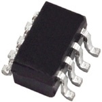
ICGOO电子元器件商城为您提供AD5060ARJZ-1REEL7由Analog设计生产,在icgoo商城现货销售,并且可以通过原厂、代理商等渠道进行代购。 AD5060ARJZ-1REEL7价格参考。AnalogAD5060ARJZ-1REEL7封装/规格:数据采集 - 数模转换器, 16 位 数模转换器 1 SOT-23-8。您可以下载AD5060ARJZ-1REEL7参考资料、Datasheet数据手册功能说明书,资料中有AD5060ARJZ-1REEL7 详细功能的应用电路图电压和使用方法及教程。
AD5060ARJZ-1REEL7 是由 Analog Devices Inc.(亚德诺半导体)生产的一款低功耗、单通道 12 位数模转换器(DAC)。它属于数据采集系统中的数模转换器类别,广泛应用于需要高精度和低功耗的场景。以下是其主要应用场景:

 1. 工业自动化与控制
   - 在工业控制系统中,AD5060 可用于将数字信号转换为模拟信号,以驱动执行器、电机控制器或传感器接口。
   - 它适用于 PLC(可编程逻辑控制器)、PID 控制器以及过程控制系统,提供精确的输出电压或电流。

 2. 仪器仪表
   - AD5060 的高精度特性使其适合用于测试测量设备,如示波器、信号发生器和数据记录仪。
   - 它可以生成精确的模拟信号,用于校准或测试其他电子设备。

 3. 通信系统
   - 在通信领域,AD5060 可用于基带信号生成,支持无线通信设备中的信号调制和解调。
   - 其低功耗特性非常适合便携式或电池供电的通信设备。

 4. 消费电子
   - 该 DAC 可用于音频设备中,将数字音频信号转换为模拟信号,驱动耳机放大器或扬声器。
   - 在智能家居设备中,AD5060 可用于调节灯光亮度、温度控制或其他模拟输出功能。

 5. 医疗设备
   - 在医疗领域,AD5060 可用于生成精确的模拟信号,驱动超声波探头、心电图仪或其他诊断设备。
   - 其低功耗和小封装尺寸使其非常适合便携式医疗设备。

 6. 汽车电子
   - AD5060 可用于汽车中的传感器接口、车载信息娱乐系统或自动驾驶系统的信号生成。
   - 它支持汽车环境下的低功耗和高可靠性需求。

 特性总结:
- 分辨率:12 位
- 低功耗:适合电池供电设备
- 小型封装:节省空间
- 高精度:满足苛刻的应用需求

AD5060ARJZ-1REEL7 的这些特点使其成为许多现代电子系统中不可或缺的组件,尤其在需要高效能和高精度的场景中表现优异。
| 参数 | 数值 |
| 产品目录 | 集成电路 (IC) |
| 描述 | IC DAC 16BIT SPI/SRL SOT23-8 |
| 产品分类 | |
| 品牌 | Analog Devices Inc |
| 数据手册 | |
| 产品图片 |
|
| 产品型号 | AD5060ARJZ-1REEL7 |
| rohs | 无铅 / 符合限制有害物质指令(RoHS)规范要求 |
| 产品系列 | nanoDAC™ |
| 产品培训模块 | http://www.digikey.cn/PTM/IndividualPTM.page?site=cn&lang=zhs&ptm=19145http://www.digikey.cn/PTM/IndividualPTM.page?site=cn&lang=zhs&ptm=18614http://www.digikey.cn/PTM/IndividualPTM.page?site=cn&lang=zhs&ptm=26125http://www.digikey.cn/PTM/IndividualPTM.page?site=cn&lang=zhs&ptm=26140http://www.digikey.cn/PTM/IndividualPTM.page?site=cn&lang=zhs&ptm=26150http://www.digikey.cn/PTM/IndividualPTM.page?site=cn&lang=zhs&ptm=26147 |
| 产品目录页面 | |
| 位数 | 16 |
| 供应商器件封装 | SOT-23-8 |
| 其它名称 | AD5060ARJZ-1REEL7DKR |
| 包装 | Digi-Reel® |
| 安装类型 | 表面贴装 |
| 封装/外壳 | SOT-23-8 |
| 工作温度 | -40°C ~ 85°C |
| 建立时间 | 4µs |
| 数据接口 | DSP,MICROWIRE™,QSPI™,串行,SPI™ |
| 标准包装 | 1 |
| 电压源 | 单电源 |
| 转换器数 | 1 |
| 输出数和类型 | 1 电压,单极1 电压,双极 |
| 采样率(每秒) | 250k |


- 商务部:美国ITC正式对集成电路等产品启动337调查
- 曝三星4nm工艺存在良率问题 高通将骁龙8 Gen1或转产台积电
- 太阳诱电将投资9.5亿元在常州建新厂生产MLCC 预计2023年完工
- 英特尔发布欧洲新工厂建设计划 深化IDM 2.0 战略
- 台积电先进制程称霸业界 有大客户加持明年业绩稳了
- 达到5530亿美元!SIA预计今年全球半导体销售额将创下新高
- 英特尔拟将自动驾驶子公司Mobileye上市 估值或超500亿美元
- 三星加码芯片和SET,合并消费电子和移动部门,撤换高东真等 CEO
- 三星电子宣布重大人事变动 还合并消费电子和移动部门
- 海关总署:前11个月进口集成电路产品价值2.52万亿元 增长14.8%


PDF Datasheet 数据手册内容提取
Fully Accurate 14-/16-Bit V nanoDAC™ OUT SPI Interface 2.7 V to 5.5 V, in an SOT-23 AD5040/AD5060 FEATURES FUNCTIONAL BLOCK DIAGRAM Single 14-/16-bit DAC, 1 LSB INL VREF VDD Power-on reset to midscale or zero scale Guaranteed monotonic by design POWER-ON BUF AD5040/ 3 power-down functions RESET AD5060 OUTPUT Low power serial interface with Schmitt-triggered inputs BUFFER REF(+) Small 8-lead SOT-23 package, low power REGDIASCTER DAC VOUT Fast settling time of 4 μs typically 2.7 V to 5.5 V power supply Low glitch on power-up AGND INPUT SYNC interrupt facility COLONTGRICOL CPOONWTREORL-D LOOWGNIC NREETSWISOTORRK APrPoPceLsIsC cAonTtIrOolN S 04767-001 SYNC SCLK DIN DACGND Data acquisition systems Portable battery-powered instruments Figure 1. Digital gain and offset adjustment Programmable voltage and current sources Programmable attenuators GENERAL DESCRIPTION PRODUCT HIGHLIGHTS The AD5040 and the AD5060, members of the ADI nanoDAC 1. Available in a small, 8-lead SOT-23 package. family, are low power, single 14-/16-bit buffered voltage-out 2. 14-/16-bit accurate, 1 LSB INL. DACs that operate from a single 2.7 V to 5.5 V supply. The 3. Low glitch on power-up. AD5040/AD5060 parts offer a relative accuracy specification of ±1 LSB and operation are guaranteed monotonic with a 4. High speed serial interface with clock speeds up to 30 MHz. ±1 LSB DNL specification. The parts use a versatile 3-wire serial 5. Three power-down modes available to the user. interface that operates at clock rates up to 30 MHz and is 6. Reset to known output voltage (midscale, zero scale). compatible with standard SPI®, QSPI™, MICROWIRE™, and DSP interface standards. The reference for both the AD5040 Table 1. Related Devices and AD5060 is supplied from an external V pin. A reference REF Part No. Description buffer is also provided on-chip. The AD5060 incorporates a AD5061 2.7 V to 5.5 V, 16-bit nanoDAC D/A, 4 LSB INL, SOT-23 power-on reset circuit that ensures the DAC output powers up to midscale or zero scale and remains there until a valid write AD5062 2.7 V to 5.5 V, 16-bit nanoDAC D/A,1 LSB INL, SOT-23 takes place to the device. The AD5040 and the AD5060 both AD5063 2.7 V to 5.5 V, 16-bit nanoDAC D/A, 1 LSB INL, MSOP contain a power-down feature that reduces the current con- sumption of the device to typically 330 nA at 5 V and provides software-selectable output loads while in power-down mode. The parts are put into power-down mode over the serial interface. Total unadjusted error for the parts is <2 mV. Both parts exhibit very low glitch on power-up. Rev. A Information furnished by Analog Devices is believed to be accurate and reliable. However, no responsibility is assumed by Analog Devices for its use, nor for any infringements of patents or other One Technology Way, P.O. Box 9106, Norwood, MA 02062-9106, U.S.A. rights of third parties that may result from its use. Specifications subject to change without notice. No license is granted by implication or otherwise under any patent or patent rights of Analog Devices. Tel: 781.329.4700 www.analog.com Trademarks and registered trademarks are the property of their respective owners. Fax: 781.461.3113 © 2005-2010 Analog Devices, Inc. All rights reserved.
AD5040/AD5060 TABLE OF CONTENTS Features .............................................................................................. 1 Reference Buffer ......................................................................... 15 Applications ....................................................................................... 1 Serial Interface ............................................................................ 15 General Description ......................................................................... 1 Power-On reset ........................................................................... 16 Functional Block Diagram .............................................................. 1 Software Reset ............................................................................. 16 Product Highlights ........................................................................... 1 Power-Down Modes .................................................................. 17 Revision History ............................................................................... 2 Microprocessor Interfacing ....................................................... 17 Specifications ..................................................................................... 3 Applications ..................................................................................... 19 Timing Characteristics ..................................................................... 5 Choosing a Reference for the AD5040/ AD5060 ................... 19 Absolute Maximum Ratings ............................................................ 6 Bipolar Operation Using the AD5040/ AD5060 .................... 19 ESD Caution .................................................................................. 6 Using the AD5040/AD5060 with a Galvanically Isolated Interface Chip ............................................................................. 20 Pin Configuration and Function Descriptions ............................. 7 Power Supply Bypassing and Grounding ................................ 20 Typical Performance Characteristics ............................................. 8 Outline Dimensions ....................................................................... 21 Terminology .................................................................................... 14 Ordering Guide .......................................................................... 21 Theory of Operation ...................................................................... 15 DAC Architecture ....................................................................... 15 REVISION HISTORY 1/10—Rev. 0 to Rev. A Changes to Table 2, Relative Accuracy (INL) and Endnote 1 .... 3 Updated Outline Dimensions ....................................................... 21 Changes to Ordering Guide .......................................................... 21 10/05—Revision 0: Initial Version Rev. A | Page 2 of 24
AD5040/AD5060 SPECIFICATIONS V = 5.5 V, V = 4.096 V @ R = unloaded, C = unloaded; T to T , unless otherwise noted. DD REF L L MIN MAX Table 2. A, B, and Y Grades1 Parameter Min Typ Max Unit Test Conditions/Comments STATIC PERFORMANCE Resolution 16 Bits AD5060 14 Bits AD5040 Relative Accuracy (INL)2 ±0.5 ±2 LSB −40°C to +85°C, AD5040/AD5060 A grade ±0.5 ±1 LSB −40°C to +85°C, AD5040/AD5060 B grade ±0.5 ±1.5 −40°C to +125°C, AD5060 Y grade Total Unadjusted Error (TUE)2 ±0.1 ±2.0 mV −40°C to +85°C, AD5040/AD5060 ±0.1 ±2.0 −40°C to +125°C, AD5060 Y grade Differential Nonlinearity (DNL)2 ±0.5 ±1 LSB Guaranteed monotonic, −40°C to +85°C, AD5040/AD5060 ±0.5 ±1 Guaranteed monotonic, −40°C to +125°C, Y grade Gain Error ±0.01 ±0.02 % of FSR T = −40°C to +85°C, AD5040/AD5060 A ±0.01 ±0.03 T = −40°C to +125°C AD5060 Y grade A Gain Error Temperature Coefficient 1 ppm of FSR/°C Offset Error ±0.02 ±1.5 mV T = −40°C to + 85°C, AD5040/AD5060 A ±0.02 ±2.0 T = −40°C to + 125°C, AD5060 Y grade A Offset Error Temperature Coefficient 0.5 μV/°C Full-Scale Error ±0.05 ±2.0 mV All 1s loaded to DAC register, AD5040 AD5060; T = −40°C to +85°C A ±0.05 ±2.0 All 1s loaded to DAC register, T = −40°C to +125°C, AD5060 Y grade A OUTPUT CHARACTERISTICS3 Output Voltage Range 0 V V REF Output Voltage Settling Time 4 μs ¼ scale to ¾ scale code transition to ±1 LSB, R = 5 kΩ L Output Noise Spectral Density 64 nV/√Hz DAC code = midscale, 1 kHz Output Voltage Noise 6 μV p-p DAC code = midscale , 0.1 Hz to 10 Hz bandwidth Digital-to-Analog Glitch Impulse 2 nV-s 1 LSB change around code 57386, R = 5 kΩ, C = 200 pF L L Digital Feedthrough 0. 003 nV-s DAC code = full scale DC Output Impedance (Normal) 0. 015 Ω Output impedance tolerance ±10% DC Output Impedance (Power-Down) (Output Connected to 1 kΩ Network)4 1 kΩ Output impedance tolerance ±400 Ω (Output Connected to 100 kΩ 100 kΩ Output impedance tolerance ±20 kΩ Network) Capacitive Load Stability 1 nF Loads used RL = 5 kΩ, RL = 100 kΩ, RL = ∞ Slew Rate 1. 2 V/μs ¼ scale to ¾ scale code transition to ±1 LSB, R = 5 kΩ, C = 200 pF L L Short-Circuit Current 60 ma DAC code = full scale, output shorted to GND, T = 25°C A 45 DAC code = zero scale, output shorted to V , T = 25°C DD A DAC Power-Up Time 4.5 μs Time to exit power-down mode to normal mode of AD5060, 24th clock edge to 90% of DAC final value, output unloaded DC Power Supply Rejection Ratio −92.11 db V ± 10%, DAC code = full scale DD Rev. A | Page 3 of 24
AD5040/AD5060 A, B, and Y Grades1 Parameter Min Typ Max Unit Test Conditions/Comments Wideband Spurious-Free Dynamic −67 db Output frequency = 10 kHz Range (SFDR) REFERENCE INPUT/OUTPUT V Input Range5 2 V − 50 mV REF DD Input Current (Power-Down) ±0.1 μA Zero scale loaded Input Current (Normal) ±0.5 μA DC Input Impedance 1 MΩ LOGIC INPUTS Input Current6 ±1 ±2 μA V , Input Low Voltage 0.8 V V = 4.5 V to 5.5 V IL DD 0.8 V = 2.7 V to 3.6 V DD V , Input High Voltage 2.0 V V = 2.7 V to 5.5 V IH DD 1.8 V = 2.7 V to 3.6 V DD Pin Capacitance 4 pF POWER REQUIREMENTS V 2.7 5.5 V All digital inputs at 0 V or V DD DD I (Normal Mode) DAC active and excluding load current DD V = 2.7 V to 5.5 V 1.0 1.2 mA V = V and V = GND, V = 5.0 V, DD IN DD IL DD V = 4.096 V, code = midscale REF 0. 82 1. 0 V = V and V = GND, V = 3.0 V, IN DD IL DD V = 2.7 V, code = midscale REF I (All Power-Down Modes) DD V = 2.5 V to 5.5 V 0.33 1 μA V = V and V = GND, V = 5.5 V, DD IH DD IL DD VREF = 4.096 V, code = midscale 0.065 V = V and V = GND, V = 3.0 V, IH DD IL DD V = 4.096 V, code = midscale REF 1 Temperature range for the A and B grades is −40°C to + 85° C, typical at 25°C; temperature range for the Y grade is −40°C to +125°C. 2 Linearity calculated using a reduced code range (160 to code 65535 for AD5060 ) and (40 to code 16383 for AD5040). 3 Guaranteed by design and characterization, not production tested. 4 1 kΩ power-down network not available with the AD5040. 5 The typical output supply headroom performance for various reference voltages at −40°C can be seen in Figure 26. 6 Total current flowing into all pins. Rev. A | Page 4 of 24
AD5040/AD5060 TIMING CHARACTERISTICS VDD = 2.7 V to 5.5 V; all specifications TMIN to TMAX, unless otherwise noted. Table 3. Parameter Limit1 Unit Test Conditions/Comments t 2 33 ns min SCLK cycle time 1 t 5 ns min SCLK high time 2 t 3 ns min SCLK low time 3 t 10 ns min SYNC to SCLK falling edge setup time 4 t 3 ns min Data setup time 5 t 2 ns min Data hold time 6 t 0 ns min SCLK falling edge to SYNC rising edge 7 t 12 ns min Minimum SYNC high time 8 t 9 ns min SYNC rising edge to next SCLK fall ignore 9 1 All input signals are specified with tr = tf = 1 ns/V (10% to 90% of VDD) and timed from a voltage level of (VIL + VIH)/2. 2 Maximum SCLK frequency is 30 MHz. t t t t 4 2 1 9 SCLK t8 t3 t7 SYNC t 6 DIN D23 D22 D2 t5 D1 D0 D23 D22 04767-002 Figure 2. AD5060 Timing Diagram Rev. A | Page 5 of 24
AD5040/AD5060 ABSOLUTE MAXIMUM RATINGS Table 4. Stresses above those listed under Absolute Maximum Ratings Parameter Rating may cause permanent damage to the device. This is a stress VDD to GND −0.3 V to +7.0 V rating only; functional operation of the device at these or any Digital Input Voltage to GND −0.3 V to VDD + 0.3 V other conditions above those indicated in the operational VOUT to GND −0.3 V to VDD + 0.3 V section of this specification is not implied. Exposure to absolute VREF to GND −0.3 V to VDD + 0.3 V maximum rating conditions for extended periods may affect Operating Temperature Range device reliability. Industrial (A, B Grade) −40°C to +85°C Extended Automotive Temperature −40°C to +125°C This device is a high performance integrated circuit with an Range (Y Grade) ESD rating of <2 kV. It is ESD sensitive. Proper precautions Storage Temperature Range −65°C to +150°C should be taken for handling and assembly. Maximum Junction Temperature 150°C SOT-23 Package Power Dissipation (T max − T )/θ J A JA θ Thermal Impedance 206°C/W JA θ Thermal Impedance 91°C/W Jc Reflow Soldering (Pb-free) Peak Temperature 260°C Time-at-Peak Temperature 10 sec to 40 sec ESD (AD5040/AD5060) 1. 5 kV ESD CAUTION ESD (electrostatic discharge) sensitive device. Electrostatic charges as high as 4000 V readily accumulate on the human body and test equipment and can discharge without detection. Although this product features proprietary ESD protection circuitry, permanent damage may occur on devices subjected to high energy electrostatic discharges. Therefore, proper ESD precautions are recommended to avoid performance degradation or loss of functionality. Rev. A | Page 6 of 24
AD5040/AD5060 PIN CONFIGURATION AND FUNCTION DESCRIPTIONS DIN 1 8 SCLK AD5040/ VDD 2 AD5060 7 SYNC TOP VIEW VREF 3 (Not to Scale) 6 DACGND VOUT 4 5 AGND 04767-003 Figure 3. Pin Configuration Table 5. Pin Function Descriptions Pin No. Mnemonic Description 1 DIN Serial Data Input. These parts have a 16-/24-bit shift register. Data is clocked into the register on the falling edge of the serial clock input. 2 V Power Supply Input. These parts can be operated from 2.7 V to 5.5 V and V should be decoupled to GND. DD DD 3 V Reference Voltage Input. REF 4 V Analog Output Voltage from DAC. OUT 5 AGND Ground Reference Point for Analog Circuitry. 6 DACGND Ground Input to the DAC Core. 7 SYNC Level-Triggered Control Input (Active Low). This is the frame synchronization signal for the input data. When SYNC goes low, it enables the input shift register and data is transferred in on the falling edges of the following clocks. The DAC is updated following the 16th/24th clock cycle unless SYNC is taken high before this edge, in which case the rising edge of SYNC acts as an interrupt, and the write sequence is ignored by the DAC. 8 SCLK Serial Clock Input. Data is clocked into the input shift register on the falling edge of the serial clock input. Data can be transferred at rates up to 30 MHz. Rev. A | Page 7 of 24
AD5040/AD5060 TYPICAL PERFORMANCE CHARACTERISTICS 1.6 0.6 1.4 VVDRDEF = = 5 4.5.0V96V 0.5 VVDRDEF = = 5 4.5.0V96V 1.2 TA = 25°C 0.4 TA = 25°C 1.0 0.8 0.3 0.6 SB) 0.4 SB) 0.2 L L 0.1 R ( 0.2 R ( O 0 O 0 R R R –0.2 R E E –0.1 L –0.4 L IN –0.6 IN –0.2 –0.8 –0.3 –1.0 –0.4 –––111...642 04767-040 ––00..65 04767-061 160 10160 20160 30160 40160 50160 60160 160 2260 4360 6460 8560 10660 12760 14860 DAC CODE DAC CODE Figure 4. Typical AD5060 INL Plot Figure 7. Typical AD5040 INL Plot 1.6 0.40 1.4 VDD = 5.5V 0.35 VDD = 5.5V VREF = 4.096V VREF = 4.096V 1.2 TA = 25°C 0.30 TA = 25°C 1.0 0.25 0.8 0.20 B) 0.6 B) 0.15 S 0.4 S 0.10 L L R ( 0.2 R ( 0.05 RO 0 RO 0 ER –0.2 ER –0.05 NL –0.4 NL –0.10 D –0.6 D –0.15 –0.8 –0.20 –1.0 –0.25 –––111...642 04767-039 –––000...433050 04767-060 160 10160 20160 30160 40160 50160 60160 160 2260 4360 6460 8560 10660 12760 14860 DAC CODE DAC CODE Figure 5. Typical AD5060 DNL Plot Figure 8. Typical AD5040 DNL Plot 0.10 0.020 VDD = 5.5V VDD = 5.5V 0.08 VTAR E=F 2=5 °4C.096V 0.015 TVAR E=F 2=5 °4C.096V 0.06 0.010 0.04 R (mV) 0.02 R (mV) 0.005 RO 0 RO 0 R R E E UE –0.02 UE –0.005 T T –0.04 –0.010 –0.06 ––00..1008 04767-041 ––00..002105 04767-062 160 10160 20160 30160 40160 50160 60160 160 2260 4360 6460 8560 10660 12760 14860 16960 DAC CODE DAC CODE Figure 6. Typical AD5060 TUE Plot Figure 9. Typical AD5040 TUE Plot Rev. A | Page 8 of 24
AD5040/AD5060 1.6 1.8 1.4 TA = 25°C 1.6 VDD = 5.5V, VREF = 4.096V 1.2 1.4 VDD = 2.7V, VREF = 2.0V 1.0 1.2 MAX OFFSET ERROR @ 1.0 0.8 0.8 MAX OFFSET ERROR @ VDD = 2.7V R (LSB) 000...246 MAX INL ERROR @ VDD = 5.5V ROR (mV) 000...246 VDD = 5.5V MIN OFFSET ERROR @ O 0 R 0 RR –0.2 T E –0.2 VDD = 5.5V INL E ––00..64 MIN INL ERROR @ VDD = 5.5V OFFSE ––00..64 MIN OFFSET ERROR @ –0.8 –0.8 VDD = 2.7V –1.0 –1.0 –1.2 –––111...642 04767-009 –––111...864 04767-067 2.0 2.5 3.0 3.5 4.0 4.5 5.0 5.5 –40 –20 0 20 40 60 80 100 120 140 REFERENCE VOLTAGE (V) TEMPERATURE (°C) Figure 10. INL vs. Reference Input Voltage1 Figure 13. Typical Offset Error vs. Temperature1 1.6 0.5 1.4 TA = 25°C VDD = 5.5V, VREF = 4.096V 1.2 0.4 VDD = 2.7V, VREF = 2.0V 1.0 0.3 0.8 MAX GAIN ERROR @ DNL ERROR (LSB) –––000000......6422460 MMINA XD NDLN LE RERRORRO R@ @ V DVDD D= =5. 55V.5V AIN ERROR (% FSR) –000...1120 MMAINX GGAAIINN VVEEDDRRDDRR ==OO 55RR.. 55@@VV VDD = 2.7V G –0.2 MIN GAIN ERROR @ –0.8 VDD = 2.7V –1.0 –0.3 –––111...642 04767-010 ––00..54 04767-066 2.0 2.5 3.0 3.5 4.0 4.5 5.0 5.5 –40 –20 0 20 40 60 80 100 120 140 REFERENCE VOLTAGE (V) TEMPERATURE (°C) Figure 11. DNL vs. Reference Input Voltage1 Figure 14. Typical Gain Error vs. Temperature1 1.2 1.4 TA = 25°C VDD = 5.5V, VREF = 4.096V 1.0 1.2 VDD = 2.7V, VREF = 2.0V 0.8 1.0 0.6 0.8 TUE ERROR (mV) ––0000....42240 MMINA XT UTEU EE RERRORRO R@ @ V DVDD D= =5. 55V.5V INL ERROR (LSB) –0000....02246 MIN INMLA VXED RIDNR L=O VE5RD.R 5D@RV =O 2R. 7@V MVDADX = I N5L.5 EVRROR @ –0.6 –0.4 MIN INL ERROR @ –0.8 –0.6 VDD = 2.7V ––11..20 04767-011 ––10..08 04767-069 2.0 2.5 3.0 3.5 4.0 4.5 5.0 5.5 –40 –20 0 20 40 60 80 100 120 140 REFERENCE VOLTAGE (V) TEMPERATURE (°C) Figure 12. TUE vs. Reference Input Voltage1 Figure 15. Typical INL Error vs. Temperature1 1 AD5060 only. Rev. A | Page 9 of 24
AD5040/AD5060 1.0 1.8 VDD = 5.5V, VREF = 4.096V VDD = 5.5V FULL-SCALE 0.8 VDD = 2.7V, VREF = 2.0V 1.6 VREF = 4.096V TA = 25°C THREE QUARTER SCALE 0.6 1.4 MAX DNL ERROR @ B) 0.4 VDD = 2.7V 1.2 S L 0.2 DNL ERROR ( –0.02 MAX DNL VEDRDR =O 5R. 5@V MIN DNL VEDRDR =O 5R. 5@V I (mA)DD 100...086 MID-SCALE QUARTER-SCALEZERO-SCALE –0.4 MIN DNL ERROR @ 0.4 –0.6 VDD = 2.7V ––10..08 04767-071 0.02 04767-044 –40 –20 0 20 40 60 80 100 120 140 0 5M 10M 15M 20M 25M 30M 35M 40M 45M TEMPERATURE (°C) FREQUENCY (Hz) Figure 16. Typical DNL Error vs. Temperature1 Figure 19. Typical Supply Current vs. Frequency @ 5.5 V1 1.0 1.6 VDD = 5.5V, VREF = 4.096V VDD = 3V 0.8 VDD = 2.7V, VREF = 2.0V 1.4 VTAR E=F 2=5 °2C.5V 0.6 MAX TUE ERROR @ 1.2 THREE QUARTER SCALE 0.4 VDD = 5.5V FULL-SCALE V) m 0.2 MAX TUE ERROR @ 1.0 OR ( VDD = 2.7V mA) ERR 0 MIN TUE ERROR @ (DD 0.8 MID-SCALE QUARTER-SCALE UE –0.2 VDD = 5.5V I 0.6 T –0.4 ZERO-SCALE MIN TUE ERROR @ 0.4 –0.6 VDD = 2.7V ––10..08 04767-068 0.02 04767-045 –40 –20 0 20 40 60 80 100 120 140 0 5M 10M 15M 20M 25M 30M 35M 40M 45M TEMPERATURE (°C) FREQUENCY (Hz) Figure 17. Typical TUE Error vs. Temperature1 Figure 20. Typical Supply Current vs. Frequency @ 3 V1 1.4 2.0 1.2 VVDDDD == 52..57VV,, VVRREEFF == 42..009V6V MAX IDD @ 1.8 TVCARO E=DF E 2= 5= °2 CM.5IVDSCALE VDD = 5.5V 1.6 1.0 1.4 1.2 I (mA)DD 00..68 MVADDX =ID 2D. 7@V I (A)μDD 10..08 0.4 0.6 0.4 0.2 0 04767-072 0.20 04767-015 –40 –20 0 20 40 60 80 100 120 140 2.5 3.0 3.5 4.0 4.5 5.0 5.5 6.0 TEMPERATURE (°C) SUPPLY VOLTAGE (V) Figure 18. Typical Supply Current vs. Temperature1 Figure 21. Typical Supply Current vs. Supply Voltage1 1 AD5060 only. Rev. A | Page 10 of 24
AD5040/AD5060 3.00 TA = 25°C VDD = 3V 2.75 DAC = FULL SCALE 2.50 VREF = 2.7V TA = 25°C 2.25 2.00 1.75 A) (mD 1.50 VDD = 5.5V, VREF = 4.096V ID 1.25 1.00 0.75 VDD = 3.0V, VREF = 2.5V 0.50 0.250 04767-014 YX AAXXIISS == 24μs/VD/DIVIV 04767-020 0 10000 20000 30000 40000 50000 60000 70000 DAC CODE Figure 22. Typical Supply Current vs. Digital Input Code1 Figure 25. 0.1 Hz to 10 Hz Noise Plot 0.50 24TH CLOCK FALLING 0.45 0.40 0.35 CH1 = SCLK M (V) 0.30 O O 0.25 R CH2 = VOUT AD 0.20 E H 0.15 0.10 04767-017 0.050 04767-091 CH2 50mV/DIV CH1 2V/DIV TIME BASE 400ns/DIV 2.7 2.9 3.1 3.3 3.5 3.7 3.9 4.1 4.3 4.5 4.7 4.9 5.1 5.3 5.5 REFERENCE VOLTAGE (V) Figure 23. AD5060 Digital-to-Analog Glitch Impulse Figure 26. VDD Headroom vs. Reference Voltage (See Figure 24) 0.117 5.05 0.116 VVDRDEF = = 5 4V.096V 5.00 VTAD D= =2 55°.0CV 0.115 R = 5kΩ DAC = FULL-SCALE 0.114 C = 220pF 4.95 0.113 CODE = 57386 V) 0.112 GE ( 4.90 AMPLITUDE 00000.....111110001178910 UTPUT VOLTA 444...887505 O 0.106 C 4.70 A 0.105 D 0.104 4.65 000...111000123 04767-043 44..6505 04767-042 0505050505050505050505 4.704.724.744.764.784.804.824.844.864.884.904.924.944.964.985.00 257025702570257025702 111122SA2MP2LE3S 333444455 VREF (V) Figure 24. AD5060 Digital-to-Analog Glitch Energy Figure 27. Output Voltage vs. Reference Voltage 1 AD5060 only. Rev. A | Page 11 of 24
AD5040/AD5060 5.005 VREF = 5V C4 = 143mV p-p TA = 25°C 5.000 ZERO-SCALE 1kΩ TO GND V) 4.995 T ( U P T 4.990 U O C A D 4.985 4.980 4.975 04767-065 04767-047 5.50 5.45 5.40 5.35 5.30 5.25 5.20 5.15 5.10 5.05 5.00 CH4 50.0mV M4.00μs CH1 1.64V VDD (V) Figure 28. Typical Output vs. Supply Voltage Figure 31. Glitch upon Entering Software Power-Down to Zero Scale C4 = 50mV p-p CH3 = SCLK 1kΩ TO GND ZERO-SCALE CH2 = VOUT CH1 = TRIGGER 04767-019 04767-048 CH1 2V/DIV CH2 2V/DIV CH3 2V TIME BASE = 5.00μs CH4 20.0mV M1.00μs CH1 1.64V Figure 29. Time to Exit Power-Down to Midscale Figure 32. Glitch upon Exiting Software Power-Down to Zero Scale 400 VDD = 5V Hz) 350 FULL-SCALE TVAR E=F 2=5 °4C.096V C252mV p-p V/ 300 n SITY ( 250 2 T C4.396V p-p N E 200 MID-SCALE D C3 FALL L 935.0μs RA 150 T PEC 100 QUARTER-SCALE C∞s3 RISE SE S 50 T NEDOG VEALID OI N –500100 1k ZERO-SCAL10Ek 100k 1M04767-046 3 CH3 2.00V CH2 50mV M1.00ms CH3 1.36V 04767-049 FREQUENCY (Hz) Figure 30. Noise Spectral Density Figure 33. Glitch upon Entering Hardware Power-Down to Three-State Rev. A | Page 12 of 24
AD5040/AD5060 2.1 VDD = 5.5V C2 2.0 V10R%EF T=O 4 9.009%6V RISE TIME = 0.688μs 30mV p-p 1.9 SLEW RATE = 1.16V/μs 2.04V 1.8 2 T C4.396V p-p 1.7 1.6 C3 FALL ∞s 1.5 NO VALID EDGE 1.4 DAC OUTPUT T C3 RISE 1.3 946.2μs 1.2 3 04767-050 11..01 1.04V 04767-052 CH3 2.00V CH2 50mV M1.00ms CH3 1.36V –10μs–8μs –6μs –4μs –2μs 0 2μs 4μs 6μs 8μs 9.96μs Figure 34. Glitch upon Exiting Hardware Power-Down to Zero Scale Figure 37. Typical Output Slew Rate 0.0010 16 CODE = MID-SCALE 0.0008 VDD = 5V, VREF = 4.096V 14 VDD = 3V, VREF = 2.5V 0.0006 12 0.0004 GE (V) 0.0002 NCY 10 OLTA 0 EQUE 8 V R Δ–0.0002 VDD = 5.5V F 6 –0.0004 4 ––00..00000068 VDD = 3V 04767-051 02 04767-075 –25 –20 –15 –10 –5 0 5 10 15 20 25 30 0.83 0.84 0.85 0.86 0.87 0.88 0.89 0.90 0.91 MORE CURRENT (mA) BIN Figure 35. Typical Output Load Regulation Figure 38. IDD Histogram VDD = 3.0 V 0.10 14 CODE = MIDSCALE 0.08 VDD = 5V, VREF = 4.096V VDD = 3V, VREF = 2.5V 12 0.06 VDD = 3V, VREF = 2.5V 0.04 10 Δ V (V)OUT –00..00202 REQUENCY 68 F –0.04 4 –0.06 VDD = 5V, VREF = 4.096V 2 ––00..1008 04767-063 0 04767-076 –25 –20 –15 –10 –5 0 5 10 15 20 25 30 1.001.011.021.031.041.051.061.071.081.091.101.11MORE IOUT (mA) BIN Figure 36. Typical Current Limiting Plot Figure 39. IDD Histogram VDD = 5.0 V Rev. A | Page 13 of 24
AD5040/AD5060 TERMINOLOGY Relative Accuracy Total Unadjusted Error (TUE) For the DAC, relative accuracy or integral nonlinearity (INL) is Total unadjusted error is a measure of the output error taking a measure of the maximum deviation, in LSBs, from a straight all the various errors into account. A typical AD5060 TUE vs. line passing through the endpoints of the DAC transfer code plot is shown in Figure 6. function. A typical AD5060 INL vs. code plot is shown in Offset Error Drift Figure 4. This is a measure of the change in zero-code error with a Differential Nonlinearity (DNL) change in temperature. It is expressed in μV/°C. Differential nonlinearity is the difference between the measured Gain Error Drift change and the ideal 1 LSB change between any two adjacent This is a measure of the change in gain error with changes in codes. A specified differential nonlinearity of ±1 LSB maximum temperature. It is expressed in (ppm of full-scale range)/°C. ensures monotonicity. This DAC is guaranteed monotonic by design. A typical AD5060 DNL vs. code plot is shown in Figure 5. Digital-to-Analog Glitch Impulse Digital-to-analog glitch impulse is the impulse injected into the Offset Error analog output when the input code in the DAC register changes Offset error is a measure of the output error when zero code state. It is normally specified as the area of the glitch in nV-s (0x0000) is loaded to the DAC register. Ideally, the output and is measured when the digital input code is changed by should be 0 V. The zero-code error is always positive in the 1 LSB at the worst case code 53786; see Figure 23 and Figure 24. AD5040/AD5060 because the output of the DAC cannot go The expanded view in Figure 23 shows the glitch generated below 0 V. This is due to a combination of the offset errors in following completion of the calibration routine; Figure 24 the DAC and output amplifier. Zero-code error is expressed zooms in on this glitch. in mV. Digital Feedthrough Full-Scale Error Digital feedthrough is a measure of the impulse injected into Full-scale error is a measure of the output error when full-scale the analog output of the DAC from the digital inputs of the code (0xFFFF AD5060, 0x3FFF AD5040) is loaded to the DAC DAC, but is measured when the DAC output is not updated. It register. Ideally, the output should be V − 1 LSB. Full-scale DD is specified in nV-s and measured with a full-scale code change error is expressed in percent of full-scale range. on the data bus—that is, from all 0s to all 1s, and vice versa. Gain Error This is a measure of the span error of the DAC. It is the devia- tion in slope of the DAC transfer characteristic from ideal, expressed as a percent of the full-scale range. Rev. A | Page 14 of 24
AD5040/AD5060 THEORY OF OPERATION The AD5040/AD5060 are single 14-/16-bit, serial input, voltage SERIAL INTERFACE output DACs. The parts operate from supply voltages of 2.7 V The AD5060/AD5040 have a 3-wire serial interface (SYNC, to 5.5 V. Data is written to the AD5060 in a 24-bit word format, SCLK, and DIN), which is compatible with SPI, QSPI, and and to the AD5040 in a 16-bit word format, via a 3-wire serial MICROWIRE interface standards, as well as most DSPs. interface. Figure 2 shows a timing diagram of a typical AD5060 write Both the AD5040 and AD5060 incorporate a power-on reset sequence. circuit that ensures the DAC output powers up to a known out- The write sequence begins by bringing the SYNC line low. For put state (midscale or zero-scale, see the Ordering Guide). The devices also have a software power-down mode that reduces the the AD5060, data from the DIN line is clocked into the 24-bit typical current consumption to less than 1 μa. shift register on the falling edge of SCLK. The serial clock frequency can be as high as 30 MHz, making these parts DAC ARCHITECTURE compatible with high speed DSPs. On the 24th falling clock The DAC architecture of the AD5060 consists of two matched edge, the last data bit is clocked in and the programmed DAC sections. A simplified circuit diagram is shown in function is executed (that is, a change in the DAC output or a Figure 40. The 4 MSBs of the 16-bit data-word are decoded to change in the mode of operation). drive 15 switches, E1 to E15. Each of these switches connects 1 of 15 matched resistors to either DACGND or the V buffer At this stage, the SYNC line can be kept low or be brought REF output. The remaining 12 bits of the data-word drive switches high. In either case, it must be brought high for a minimum of S0 to S11 of a 12-bit voltage mode R-2R ladder network. 12 ns before the next write sequence so that a falling edge of SYNC can initiate the next write sequence. Because the SYNC VOUT buffer draws more current when V = 1.8 V than it does when IH 2R 2R 2R 2R 2R 2R 2R V = 0.8 V, SYNC should be idled low between write sequences IH S0 S1 S11 E1 E2 E15 for an even lower power operation of the part. As previously VREF indicated, however, it must be brought high again just before the next write sequence. The AD5040 requires 16 clock periods 12-BIT R-2R LADDER FOU15R EMQSUBAsL D SEECGOMDEENDT ISNTO 04767-027 ttoh eu lpadsta tdea ttha eb iint pisu ctl oshcikfet dr eigni satnedr. tOhne pthroe g1r6atmh mfaelldin fgu nclcotciokn e disg e, Figure 40. AD5060 DAC Ladder Structure executed (that is, a change in the DAC output or a change in the mode of operation). REFERENCE BUFFER Input Shift Register The AD5040 andAD5060 operate with an external reference. The reference input (V ) has an input range of 2 V to The AD5060 input shift register is 24 bits wide; see Figure 41. REF V − 50 mV. This input voltage is then used to provide a PD1 and PD0 are control bits that control the operating mode DD buffered reference for the DAC core. of the part—normal mode or any one of three power-down modes (see the Power-Down Modes section for more detail). The next 16 bits are the data bits. These are transferred to the DAC register on the 24th falling edge of SCLK. DB15 (MSB) DB0 (LSB) 0 0 0 0 0 0 PD1 PD0 D15 D14 D13 D12 D11 D10 D9 D8 D7 D6 D5 D4 D3 D2 D1 D0 DATA BITS 0 0 NORMAL OPERATION 0 1 3-STATE 11 01 110k0Ωk TΩO T GON GDND POWER-DOWN MODES 04767-028 Figure 41. AD5060 Input Register Content Rev. A | Page 15 of 24
AD5040/AD5060 The AD5040 input shift register is 16 bits wide; see Figure 42. POWER-ON RESET PD1 and PD0 are control bits that control the operating mode The AD5040 and AD5060 both contain a power-on reset of the part—normal mode or any one of two power-down circuit that controls the output voltage during power-up. The modes (see Power-Down Modes section for more detail). The DAC register is filled with the zero-scale code or midscale code next 14 bits are the data bits. These are transferred to the DAC and the output voltage is set to zero scale or midscale (see the register on the 16th falling edge of SCLK. Ordering Guide for more details on the reset model). It remains SYNC Interrupt there until a valid write sequence is made to the DAC. This is useful in applications where it is important to know the output In a normal write sequence for the AD5060, the SYNC line is state of the DAC while it is in the process of powering up. kept low for at least 24 falling edges of SCLK, and the DAC is updated on the 24th falling edge. However, if SYNC is brought SOFTWARE RESET high before the 24th falling edge, the write sequence is The AD5060 device can be put into software reset by setting all interrupted. The shift register is reset and the write sequence is bits in the DAC register to 1; this includes writing 1s to Bit D23 considered invalid. Neither an update of the DAC register and Bit D16, which is not the normal mode of operation. For contents nor a change in the operating mode occurs; see Figure the AD5040 this includes writing 1s to Bit D15 and Bit D14, 43. In a normal write sequence for the AD5040, the SYNC line which is also not the normal mode of operation. Note that the is kept low for at least 16 falling edges of SCLK, and the DAC is SYNC interrupt command cannot be performed if a software updated on the 16th falling edge. However, if SYNC is brought reset command is started in the AD5040 or AD5060. high before the 16th falling edge, the write sequence is interrupted. The shift register is reset and the write sequence is considered invalid. Neither an update of the DAC register contents nor a change in the operating mode occurs. DB13 (MSB) DB0 (LSB) PD1 PD0 D13 D12 D11 D10 D9 D8 D7 D6 D5 D4 D3 D2 D1 D0 DATA BITS 0 0 NORMAL OPERATION 0 1 3-STATE 1 0 100kΩ TO GND POWER-DOWN MODES 04767-074 Figure 42. AD5040 Input Register Content SCLK SYNC DIN DBIN23VALID WRITE SEQUENDCBE0: VALID WDBR2I3TE SEQUENCE, OUTPUDTB 0UPDATES 04767-031 SYNC HIGH BEFORE 24TH FALLING EDGE ON THE 24TH FALLING EDGE Figure 43. AD5060 SYNC Interrupt Facility Rev. A | Page 16 of 24
AD5040/AD5060 MICROPROCESSOR INTERFACING POWER-DOWN MODES AD5040/AD5060 to ADSP-2101/ADSP-2103 Interface The AD5060 features four operating modes, and the AD5040 features three operating modes. These modes are software pro- Figure 45 shows a serial interface between the AD5040/AD5060 grammable by setting two bits in the control register (Bit DB17 and the ADSP-2101/ADSP-2103. The ADSP-2101/ADSP-2103 and Bit DB16 in the AD5060 and Bit DB15 and Bit DB14 in the should be set up to operate in the SPORT transmit alternate AD5040). Table 6 and Table 7 show how the state of the bits framing mode. The ADSP-2101/ADSP-2103 sport is pro- corresponds to the operating mode of the two devices. grammed through the SPORT control register and should be configured for internal clock operation, active low framing, and Table 6. Operating Modes for the AD5060 16-bit word length. Transmission is initiated by writing a word DB17 DB16 Operating Mode to the Tx register after the SPORT has been enabled. 0 0 Normal operation Power-down modes: ADSP-2101/ AD5040/ 0 1 3-state ADSP-21031 AD50601 1 0 100 kΩ to GND 1 1 1 kΩ to GND TFS SYNC DT DIN TDaBb1l5e 7. OperaDtBin1g4 Modes foOrp tehrea tAinDg5 M04o0d e SCLK SCLK 04767-030 0 0 Normal operation 1ADDITIONAL PINS OMITTED FOR CLARITY Power-down modes: Figure 45. AD5040/AD5060 to ADSP-2101/ADSP-2103 Interface 0 1 3-state AD5040/AD5060 to 68HC11/68L11 Interface 1 0 100 kΩ to GND 1 1 See Software Reset section Figure 46 shows a serial interface between the AD5040/ AD5060 and the 68HC11/68L11 microcontroller. SCK of the 68HC11/68L11 drives the SCLK pin of the AD5040/AD5060, In both the AD5060 and the AD5040, when the two most while the MOSI output drives the serial data line of the DAC. significant bits are set to 0, the part has normal power The SYNC signal is derived from a port line (PC7). The setup consumption. However, for the three power-down modes of the conditions for correct operation of this interface require that the AD5060 and the two power down modes of the AD5040, the 68HC11/68L11 be configured so that its CPOL bit is 0 and its supply current falls to less than 1μA at 5 V (65 nA at 3 V). Not CPHA bit is 1. When data is being transmitted to the DAC, the only does the supply current fall, but the output stage is also SYNC line is taken low (PC7). When the 68HC11/68L11 is internally switched from the output of the amplifier to a resistor network of known values. This is advantageous because the configured where its CPOL bit is 0 and its CPHA bit is 1, data output impedance of the part is known while the part is in appearing on the MOSI output is valid on the falling edge of power-down mode. The output is connected internally to GND SCK. Serial data from the 68HC11/68L11 is transmitted in 8-bit through a 1 kΩ resistor (AD5060 only) or a 100 kΩ resistor, or bytes with only 8 falling clock edges occurring in the transmit it is left open-circuited (three-stated). The output stage is cycle. Data is transmitted MSB first. In order to load data to the illustrated in Figure 44. AD5040/AD5060, PC7 is left low after the first eight bits are transferred, and a second serial write operation is performed to OUTPUT BUFFER the DAC. PC7 is taken high at the end of this procedure. AD5040/ AD5060 VOUT DAC 68HC11/ AD5040/ 68L111 AD50601 POWER-DOWN PC7 SYNC CIRCUITRY RESISTOR NETWORK SCK SCLK 04767-029 MOSI DIN 04767-032 Figure 44. Output Stage During Power-Down 1ADDITIONAL PINS OMITTED FOR CLARITY The bias generator, the DAC core, and other associated linear Figure 46. AD5040/AD5060 to 68HC11/68L11 Interface circuitry are all shut down when power-down mode is activated. However, the contents of the DAC register are unaffected when in power-down. The time to exit power-down is typically 2.5 μs for V = 5 V, and 5 μs for V = 3 V; DD DD see Figure 29. Rev. A | Page 17 of 24
AD5040/AD5060 AD5040/AD5060 to Blackfin® ADSP-BF53x Interface AD5040/AD5060 to MICROWIRE Interface Figure 47 shows a serial interface between the AD5040/ Figure 49 shows an interface between the AD5040/AD5060 and AD5060 and the Blackfin ADSP-53x microprocessor. The any MICROWIRE-compatible device. Serial data is shifted out ADSP-BF53x processor family incorporates two dual-channel on the falling edge of the serial clock and is clocked into the synchronous serial ports, SPORT1 and SPORT0, for serial and AD5040/AD5060 on the rising edge of the SK. multiprocessor communications. Using SPORT0 to connect to the AD5040/AD5060, the setup for the interface is: DT0PRI MICROWIRE1 AD5040/ AD50601 drives the SDIN pin of the AD5040/AD5060, while TSCLK0 drives the SCLK of the part; the SYNC is driven from TFS0. CS SYNC SK SCLK ADSP-BF53x1 AADD550064001/ SO DIN 04767-035 DT0PRI DIN 1ADDITIONAL PINS OMITTED FOR CLARITY TSCLK0 SCLK Figure 49. AD5040/AD5060 to MICROWIRE Interface TFS0 SYNC 04767-033 1ADDITIONAL PINS OMITTED FOR CLARITY Figure 47. AD5040/AD5060 to Blackfin® ADSP-BF53x Interface AD5040/AD5060 to 80C51/80L51 Interface Figure 48 shows a serial interface between the AD5060/ AD5040 and the 80C51/80L51 microcontroller. The setup for the interface is: TxD of the 80C51/80L51 drives SCLK of the AD5040/AD5060 while RxD drives the serial data line of the part. The SYNC signal is again derived from a bit- programmable pin on the port. In this case, Port Line P3.3 is used. When data is to be transmitted to the AD5040, P3.3 is taken low. The 80C51/80L51 transmits data only in 8-bit bytes; thus only 8 falling clock edges occur in the transmit cycle. To load data to the DAC, P3.3 is left low after the first eight bits are transmitted, and a second write cycle is initiated to transmit the second byte of data. P3.3 is taken high following the completion of this cycle. The 80C51/80L51 outputs the serial data in a format which has the LSB first. The AD5040/AD5060 require data to be received with the MSB as the first bit. The 80C51/80L51 transmit routine should take this into account. 80C51/80L511 AD5040/ AD50601 P3.3 SYNC TxD SCLK RxD DIN 04767-034 1ADDITIONAL PINS OMITTED FOR CLARITY Figure 48. AD5040/AD5060 to 80C51/80L51 Interface Rev. A | Page 18 of 24
AD5040/AD5060 APPLICATIONS CHOOSING A REFERENCE FOR THE AD5040/ output noise in the 0.1 Hz to 10 Hz region. Table 8 shows examples of recommended precision references for use as a AD5060 supply to the AD5040/AD5060. To achieve the optimum performance from the AD5040/ Table 8. Precision References for the AD5040/AD5060 AD5060, carefully choose a precision voltage reference. The Initial AD5040/AD5060 have just one reference input, V . The REF Accuracy Temp. Drift 0.1 Hz to 10 Hz voltage on the reference input is used to supply the positive Part No. (mV max) (ppm/°C max) Noise (μV p-p typ) input to the DAC. Therefore, any error in the reference is ADR435 ±2 3 (SO-8) 8 reflected in the DAC. ADR425 ±2 3 (SO-8) 3.4 There are four possible sources of error to consider when ADR02 ±3 3 (SO-8) 10 choosing a voltage reference for high accuracy applications: ADR02 ±3 3 (SC70) 10 initial accuracy, ppm drift, long-term drift, and output voltage ADR395 ±5 9 (TSOT-23) 8 noise. Initial accuracy on the output voltage of the DAC leads to a full-scale error in the DAC. To minimize these errors, a BIPOLAR OPERATION USING THE AD5040/ reference with high initial accuracy is preferred. Also, choosing AD5060 a reference with an output trim adjustment, such as an ADR43x The AD5040/AD5060 have been designed for single-supply device, allows a system designer to trim out system errors by operation, but a bipolar output range is also possible using the setting a reference voltage to a voltage other than the nominal. circuit in Figure 51. The circuit shown yields an output voltage The trim adjustment can also be used at temperature to trim range of ±5 V. Rail-to-rail operation at the amplifier output is out any errors. achievable using an AD8675/AD820/AD8032 or an OP196/ OP295. Because the supply current required by the AD5040/AD5060 is extremely low, the parts are ideal for low supply applications. The output voltage for any input code can be calculated as The ADR395 voltage reference is recommended. This requires less than 100 μA of quiescent current and can, therefore, drive ⎡ ⎛ D ⎞ ⎛R1+R2⎞ ⎛R2⎞⎤ multiple DACs in one system, if required. It also provides very VO =⎢⎣VDD×⎜⎝65536⎟⎠×⎜⎝ R1 ⎟⎠−VDD×⎜⎝R1⎟⎠⎥⎦ good noise performance at 8 μV p-p in the 0.1 Hz to 10 Hz range. where D represents the input code in decimal (0 to 65536, 7V AD5060). 5V ADR395 With V = 5 V, R1 = R2 = 10 kΩ: REF ⎛10×D⎞ V =⎜ ⎟−5V 3-WIRE SYNC AD5040/ VOUT = 0V TO 5V O ⎝65536⎠ SERIAL SCLK AD5060 INTERFACE DIN 04767-036 Uwsitihn g0 xth0e0 0A0D c5o0rr6e0s,p tohnisd iisn agn t oo ua t−pu5 tV v oolutatpgeu tr aanngde 0 oxfF ±F5F FV corresponding to a +5 V output . Figure 50. ADR395 as Reference to AD5060/AD5040 R2 = 10kΩ Long-term drift is a measure of how much the reference drifts +5V over time. A reference with a tight long-term drift specification +5V R1 = 10kΩ – ensures that the overall solution remains relatively stable during AD820/ its entire lifetime. The temperature coefficient of a reference OP295 ±5V + output voltage affects INL, DNL, and TUE. A reference with a AD5040/ tight temperature coefficient specification should be chosen to VREF AD5060 VOUT –5V reduce the temperature dependence of the DAC output voltage 10μF 0.1μF on ambient conditions. In high accuracy applications, which have a relatively low noise bisu idmgpeto,r rteafnetr eton cceh oouotspeu at rveofeltraegnec ne owisiteh n aese dlosw to a nb eo cuotpnusitd neoreisde. It INTS3E-EWRRIFIRAAELCE 04767-037 voltage as practical for the system noise resolution required. Precision voltage references, such as the ADR435, produce low Figure 51. Bipolar Operation with the AD5040/AD5060 Rev. A | Page 19 of 24
AD5040/AD5060 USING THE AD5040/AD5060 WITH A GALVANICALLY ISOLATED INTERFACE CHIP POWER SUPPLY BYPASSING AND GROUNDING In process control applications in industrial environments, it is When accuracy is important in a circuit, it is helpful to carefully often necessary to use a galvanically isolated interface to protect consider the power supply and ground return layout on the and isolate the controlling circuitry from any hazardous board. The printed circuit board containing the AD5040/ common-mode voltages that can occur in the area where the AD5060 should have separate analog and digital sections, each DAC is functioning. iCoupler® provides isolation in excess of having its own area of the board. If the AD5040/AD5060 are in 2.5 kV. Because the AD5040/AD5060 use a 3-wire serial logic a system where other devices require an AGND-to-DGND interface, the ADuM130x family provides an ideal digital connection, the connection should be made at one point only. solution for the DAC interface. This ground point should be as close as possible to the AD5040/AD5060. The ADuM130x isolators provide three independent isolation The power supply to the AD5040/AD5060 should be bypassed channels in a variety of channel configurations and data rates. with 10 μF and 0.1 μF capacitors. The capacitors should be They operate across the full range from 2.7 V to 5.5 V, providing physically as close as possible to the device with the 0.1 μF compatibility with lower voltage systems as well as enabling a voltage translation functionality across the isolation barrier. capacitor ideally right up against the device. The 10 μF capacitors are the tantalum bead type. It is important that the Figure 52 shows a typical galvanically isolated configuration 0.1 μF capacitor has low effective series resistance (ESR) and using the AD5040/AD5060. The power supply to the part effective series inductance (ESI), as do common ceramic types also needs to be isolated; this is accomplished by using a of capacitors. This 0.1 μF capacitor provides a low impedance transformer. On the DAC side of the transformer, a 5 V path to ground for high frequencies caused by transient regulator provides the 5 V supply required for the currents due to internal logic switching. AD5040/AD5060. The power supply line itself should have as large a trace as 5V possible to provide a low impedance path and reduce glitch REGULATOR POWER 10μF 0.1μF effects on the supply line. Clocks and other fast switching digital signals should be shielded from other parts of the board by a digital ground. Avoid crossover of digital and analog VDD signals, if possible. When traces cross on opposite sides of the board, ensure that they run at right angles to each other to SCLK V1A V0A SCLK reduce feedthrough effects on the board. The best board layout ADuM1300 AD5040/ technique is the microstrip technique where the component AD5060 side of the board is dedicated to the ground plane only, and the SDI V1B V0B SYNC VOUT signal traces are placed on the solder side. However, this is not always possible with a two-layer board. DATA V1C V0C DIN GND 04767-038 Figure 52. AD5040/AD5060 with a Galvanically Isolated Interface Rev. A | Page 20 of 24
AD5040/AD5060 OUTLINE DIMENSIONS 3.00 2.90 2.80 1.70 8 7 6 5 3.00 1.60 2.80 1.50 2.60 1 2 3 4 PIN 1 INDICATOR 0.65 BSC 1.95 BSC 1.30 1.15 0.90 1.45 MAX 0.22 MAX 0.95 MIN 0.08 MIN 0.60 0.15 MAX 8° 0.45 0.05 MIN 0.38 MAX SPELAATNIENG 4° B0S.6C0 0.30 0.22 MIN 0° COMPLIANT TO JEDEC STANDARDS MO-178-BA 121608-A Figure 53. 8-Lead Small Outline Transistor Package [SOT-23] (RJ-8) Dimensions shown in millimeters ORDERING GUIDE Temperature Maximum Package Model1 Range INL Description Package Description Option Branding AD5040BRJZ-500RL7 −40°C to +85°C 1 LSB 2.7 V to 5.5 V, reset to 0V 8 Lead SOT-23 RJ-8 D4C AD5040BRJZ-REEL7 −40°C to +85°C 1 LSB 2.7 V to 5.5 V, reset to 0V 8 Lead SOT-23 RJ-8 D4C AD5060ARJZ-1500RL7 −40°C to +85°C 2 LSB 2.7 V to 5.5 V, reset to 0 V 8 Lead SOT-23 RJ-8 D3Z AD5060ARJZ-1REEL7 −40°C to +85°C 2 LSB 2.7 V to 5.5 V, reset to 0 V 8 Lead SOT-23 RJ-8 D3Z AD5060ARJZ-2REEL7 −40°C to +85°C 2 LSB 2.7 V to 5.5 V, reset to mid- 8 Lead SOT-23 RJ-8 D41 scale AD5060ARJZ-2500RL7 −40°C to +85°C 2 LSB 2.7 V to 5.5 V, reset tomid- 8 Lead SOT-23 RJ-8 D41 scale AD5060BRJZ-1500RL7 −40°C to +85°C 1 LSB 2.7 V to 5.5 V, reset to 0 V 8 Lead SOT-23 RJ-8 D3W AD5060BRJZ-1REEL7 −40°C to +85°C 1 LSB 2.7 V to 5.5 V, reset to 0 V 8 Lead SOT-23 RJ-8 D3W AD5060BRJZ-2REEL7 −40°C to +85°C 1 LSB 2.7 V to 5.5 V, reset to mid- 8 Lead SOT-23 RJ-8 D3X scale AD5060BRJZ-2500RL7 −40°C to +85°C 1 LSB 2.7 V to 5.5 V, reset to mid- 8 Lead SOT-23 RJ-8 D3X scale AD5060YRJZ-1500RL7 −40°C to +125°C ±1.5 LSB 2.7 V to 5.5 V, reset to 0 V 8 Lead SOT-23 RJ-8 D6F AD5060YRJZ-1REEL7 −40°C to +125°C ±1.5 LSB 2.7 V to 5.5 V, reset to 0 V 8 Lead SOT-23 RJ-8 D6F EVAL-AD5060EBZ Evaluation Board 1 Z = RoHS Compliant Part. Rev. A | Page 21 of 24
AD5040/AD5060 NOTES Rev. A | Page 22 of 24
AD5040/AD5060 NOTES Rev. A | Page 23 of 24
AD5040/AD5060 NOTES © 2005-2010 Analog Devices, Inc. All rights reserved. Trademarks and registered trademarks are the property of their respective owners. D04767-0-1/10(A) Rev. A | Page 24 of 24