ICGOO在线商城 > 集成电路(IC) > 数据采集 - 数模转换器 > MAX5815AAUD+

 Datasheet下载
- 型号: MAX5815AAUD+
- 制造商: Maxim
- 库位|库存: xxxx|xxxx
- 要求:
| 数量阶梯 | 香港交货 | 国内含税 |
| +xxxx | $xxxx | ¥xxxx |
查看当月历史价格
查看今年历史价格
MAX5815AAUD+产品简介:
ICGOO电子元器件商城为您提供MAX5815AAUD+由Maxim设计生产,在icgoo商城现货销售,并且可以通过原厂、代理商等渠道进行代购。 MAX5815AAUD+价格参考。MaximMAX5815AAUD+封装/规格:数据采集 - 数模转换器, 12 位 数模转换器 4 14-TSSOP。您可以下载MAX5815AAUD+参考资料、Datasheet数据手册功能说明书,资料中有MAX5815AAUD+ 详细功能的应用电路图电压和使用方法及教程。
MAX5815AAUD+ 是 Maxim Integrated 公司生产的一款 12 位电压输出型数模转换器(DAC),属于数据采集系统中的数模转换器类别。其主要应用场景包括以下几类:

 1. 工业控制
   - MAX5815AAUD+ 可用于工业自动化和控制系统中,将数字信号转换为模拟信号以驱动执行器、电机或传感器。例如,在过程控制中,可以调节阀门开度、控制温度或压力等参数。
   - 它的低功耗特性和高分辨率使其适合需要精确控制的应用场景。

 2. 仪器仪表
   - 在精密测量仪器中,MAX5815AAUD+ 能提供稳定的电压输出,用于校准或生成参考信号。例如,示波器、信号发生器和数据记录仪等设备可能需要 DAC 来生成精确的模拟波形。

 3. 通信系统
   - 该器件可用于通信设备中,将数字信号转换为模拟信号以实现调制解调功能。例如,在无线通信基站或有线调制解调器中,DAC 是关键组件之一。

 4. 消费电子
   - 在音频设备中,MAX5815AAUD+ 可用于将数字音频信号转换为模拟信号,驱动耳机放大器或扬声器。虽然它不是专门设计为音频 DAC,但在某些低成本应用中仍然适用。
   - 此外,它也可以用于家用电器的控制面板,如空调、洗衣机等,实现对温度、速度或其他参数的调节。

 5. 医疗设备
   - 在医疗领域,MAX5815AAUD+ 可用于便携式医疗设备中,例如血糖仪、心率监测仪等。它能够生成精确的模拟信号以驱动传感器或显示器。
   - 高分辨率特性使其适用于需要高精度信号处理的医疗应用。

 6. 汽车电子
   - 在汽车电子系统中,MAX5815AAUD+ 可用于车载信息娱乐系统、传感器接口或电源管理模块中。例如,它可以生成模拟信号来控制车灯亮度、座椅加热等功能。

 特性总结
MAX5815AAUD+ 的优势在于其单通道设计、12 位分辨率、低功耗以及小型封装(TQFN 封装)。这些特性使其非常适合空间受限且对成本敏感的应用场景。同时,其宽工作电压范围(2.7V 至 5.5V)也增加了其在不同电源环境下的适应性。
| 参数 | 数值 |
| 产品目录 | 集成电路 (IC)半导体 |
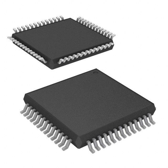
| 描述 | IC DAC 12BIT SRL 4CH 14TSSOP数模转换器- DAC 12-Bit 4Ch V DAC w/I2C Interface |
| 产品分类 | |
| 品牌 | Maxim Integrated |
| 产品手册 | |
| 产品图片 |
|
| rohs | 符合RoHS无铅 / 符合限制有害物质指令(RoHS)规范要求 |
| 产品系列 | 数据转换器IC,数模转换器- DAC,Maxim Integrated MAX5815AAUD+- |
| 数据手册 | |
| 产品型号 | MAX5815AAUD+ |
| 产品培训模块 | http://www.digikey.cn/PTM/IndividualPTM.page?site=cn&lang=zhs&ptm=25705 |
| 产品种类 | 数模转换器- DAC |
| 位数 | 12 |
| 供应商器件封装 | 14-TSSOP |
| 分辨率 | 12 bit |
| 包装 | 管件 |
| 商标 | Maxim Integrated |
| 安装类型 | 表面贴装 |
| 安装风格 | SMD/SMT |
| 封装 | Tube |
| 封装/外壳 | 14-TSSOP(0.173",4.40mm 宽) |
| 封装/箱体 | TSSOP-14 |
| 工作温度 | -40°C ~ 125°C |
| 工厂包装数量 | 96 |
| 建立时间 | 4.5µs |
| 接口类型 | Serial (2-Wire, I2C) |
| 数据接口 | I²C |
| 最大功率耗散 | 797 mW |
| 最大工作温度 | + 125 C |
| 最小工作温度 | - 40 C |
| 标准包装 | 1 |
| 电压参考 | Internal or External |
| 电压源 | 模拟和数字 |
| 电源电压-最大 | 5.5 V |
| 电源电压-最小 | 2.7 V |
| 积分非线性 | 1 LSB |
| 稳定时间 | 4.5 us |
| 系列 | MAX5815 |
| 转换器数 | 4 |
| 转换器数量 | 4 |
| 输出数和类型 | 4 电压,单极 |
| 输出类型 | Voltage Buffered |
| 采样率(每秒) | - |
| 零件号别名 | MAX5815 |


- 商务部:美国ITC正式对集成电路等产品启动337调查
- 曝三星4nm工艺存在良率问题 高通将骁龙8 Gen1或转产台积电
- 太阳诱电将投资9.5亿元在常州建新厂生产MLCC 预计2023年完工
- 英特尔发布欧洲新工厂建设计划 深化IDM 2.0 战略
- 台积电先进制程称霸业界 有大客户加持明年业绩稳了
- 达到5530亿美元!SIA预计今年全球半导体销售额将创下新高
- 英特尔拟将自动驾驶子公司Mobileye上市 估值或超500亿美元
- 三星加码芯片和SET,合并消费电子和移动部门,撤换高东真等 CEO
- 三星电子宣布重大人事变动 还合并消费电子和移动部门
- 海关总署:前11个月进口集成电路产品价值2.52万亿元 增长14.8%


PDF Datasheet 数据手册内容提取
EVALUATION KIT AVAILABLE MAX5813/MAX5814/MAX5815 Ultra-Small, Quad-Channel, 8-/10-/12-Bit Buffered Output DACs with Internal Reference and I2C Interface General Description Benefits and Features The MAX5813/MAX5814/MAX5815 4-channel, low-power, S Four High-Accuracy DAC Channels 8-/10-/12-bit, voltage-output digital-to-analog converters 12-Bit Accuracy Without Adjustment (DACs) include output buffers and an internal reference ±1 LSB INL Buffered Voltage Output that is selectable to be 2.048V, 2.500V, or 4.096V. The Guaranteed Monotonic Over All Operating MAX5813/MAX5814/MAX5815 accept a wide supply Conditions voltage range of 2.7V to 5.5V with extremely low power Independent Mode Settings for Each DAC (3mW) consumption to accommodate most low-voltage S Three Precision Selectable Internal References applications. A precision external reference input allows 2.048V, 2.500V, or 4.096V rail-to-rail operation and presents a 100kI (typ) load to S Internal Output Buffer an external reference. Rail-to-Rail Operation with External Reference The MAX5813/MAX5814/MAX5815 have an I2C-compatible, 4.5µs Settling Time 2-wire interface that operates at clock rates up to Outputs Directly Drive 2kI Loads 400kHz. The DAC output is buffered and has a low sup- S Small 5mm x 4.4mm 14-Pin TSSOP or Ultra-Small ply current of less than 250FA per channel and a low 1.6mm x 2.2mm 12-Bump WLP Package offset error of Q0.5mV (typ). On power-up, the MAX5813/ MAX5814/MAX5815 reset the DAC outputs to zero, pro- S Wide 2.7V to 5.5V Supply Range viding additional safety for applications that drive valves S Separate 1.8V to 5.5V VDDIO Power-Supply Input or other transducers which need to be off on power-up. S Fast 400kHz I2C-Compatible, 2-Wire Serial The internal reference is initially powered down to allow Interface use of an external reference. The MAX5813/MAX5814/ MAX5815 allow simultaneous output updates using soft- S Power-On-Reset to Zero-Scale DAC Output ware LOAD commands or the hardware load DAC logic S LDAC and CLR For Asynchronous Control input (LDAC). S Three Software-Selectable Power-Down Output A clear logic input (CLR) allows the contents of the CODE Impedances and the DAC registers to be cleared asynchronously and 1kI, 100kI, or High Impedance sets the DAC outputs to zero. The MAX5813/MAX5814/ MAX5815 are available in a 14-pin TSSOP and an ultra- small, 12-bump WLP package and are specified over the Functional Diagram -40NC to +125NC temperature range. Applications VDDIO VDD REF Programmable Voltage and Current Sources MAX5813 Gain and Offset Adjustment INTERNAL REFERENCE/ MAX5814 EXTERNAL BUFFER MAX5815 SCL Automatic Tuning and Optical Control 1 OF 4 DAC CHANNELS SDA Power Amplifier Control and Biasing CODE DAC 8-/10-/12-BIT ADDR0 REGISTER LATCH DAC BUFFER OUTA Process Control and Servo Loops I2C SERIAL (ADDR1) INTERFACE OUTB Portable Instrumentation CLR CLEAR/ CLEAR/ OUTC CODE RESET LOAD RESET 100kI 1kI Data Acquisition (LDAC) OUTD DAC CONTROL LOGIC POWER-DOWN POR Ordering Information appears at end of data sheet. GND ( ) TSSOP PACKAGE ONLY For related parts and recommended products to use with this part, refer to: www.maximintegrated.com/MAX5813.related For pricing, delivery, and ordering information, please contact Maxim Direct at 1-888-629-4642, or visit Maxim’s website at www.maximintegrated.com. 19-6167; Rev 4; 6/13
MAX5813/MAX5814/MAX5815 Ultra-Small, Quad-Channel, 8-/10-/12-Bit Buffered Output DACs with Internal Reference and I2C Interface ABSOLUTE MAXIMUM RATINGS VDD, VDDIO to GND ................................................-0.3V to +6V Maximum Continuous Current into Any Pin ....................Q50mA OUT_, REF to GND ....0.3V to the lower of (VDD + 0.3V) and +6V Operating Temperature Range ........................-40NC to +125NC SCL, SDA, LDAC, CLR to GND ..............................-0.3V to +6V Storage Temperature Range ............................-65NC to +150NC ADDR_ to GND ............................................-0.3V to the lower of Lead Temperature (TSSOP only)(soldering, 10s) ...........+300NC (VDDIO + 0.3V) and +6V Soldering Temperature (reflow) .................................... +260NC Continuous Power Dissipation (TA = +70NC) TSSOP (derate at 10mW/NC above 70NC) ...................797mW WLP (derate at 16.1mW/NC above 70NC) ..................1288mW Stresses beyond those listed under “Absolute Maximum Ratings” may cause permanent damage to the device. These are stress ratings only, and functional opera- tion of the device at these or any other conditions beyond those indicated in the operational sections of the specifications is not implied. Exposure to absolute maximum rating conditions for extended periods may affect device reliability. PACKAGE THERMAL CHARACTERISTICS (Note 1) TSSOP WLP Junction-to-Ambient Thermal Resistance (θJA) .......100NC/W Junction-to-Ambient Thermal Resistance (θJA) Junction-to-Case Thermal Resistance (θJC) ..............30NC/W (Note 2) ........................................................................62NC/W Note 1: Package thermal resistances were obtained using the method described in JEDEC specification JESD51-7, using a four-layer board. For detailed information on package thermal considerations, refer to www.maximintegrated.com/thermal-tutorial. Note 2: Visit www.maximintegrated.com/app-notes/index.mvp/id/1891 for information about the thermal performance of WLP packaging. ELECTRICAL CHARACTERISTICS (VDD = 2.7V to 5.5V, VDDIO = 1.8V to 5.5V, VGND = 0V, CL = 200pF, RL = 2kI, TA = -40NC to +125NC, unless otherwise noted. Typical values are at TA = +25NC.) (Note 3) PARAMETER SYMBOL CONDITIONS MIN TYP MAX UNITS DC PERFORMANCE (Note 4) MAX5813 8 Resolution and Monotonicity N MAX5814 10 Bits MAX5815 12 MAX5813 -0.25 Q0.05 +0.25 Integral Nonlinearity (Note 5) INL MAX5814 -0.5 Q0.25 +0.5 LSB MAX5815 -1 Q0.5 +1 MAX5813 -0.25 Q0.05 +0.25 Differential Nonlinearity (Note 5) DNL MAX5814 -0.5 Q0.1 +0.5 LSB MAX5815 -1 Q0.2 +1 Offset Error (Note 6) OE -5 Q0.5 +5 mV Offset Error Drift Q10 FV/NC Gain Error (Note 6) GE -1.0 Q0.1 +1.0 %FS ppm of Gain Temperature Coefficient With respect to VREF Q3.0 FS/NC Zero-Scale Error 0 10 mV Full-Scale Error With respect to VREF -0.5 +0.5 %FS Maxim Integrated 2
MAX5813/MAX5814/MAX5815 Ultra-Small, Quad-Channel, 8-/10-/12-Bit Buffered Output DACs with Internal Reference and I2C Interface ELECTRICAL CHARACTERISTICS (continued) (VDD = 2.7V to 5.5V, VDDIO = 1.8V to 5.5V, VGND = 0V, CL = 200pF, RL = 2kI, TA = -40NC to +125NC, unless otherwise noted. Typical values are at TA = +25NC.) (Note 3) PARAMETER SYMBOL CONDITIONS MIN TYP MAX UNITS DAC OUTPUT CHARACTERISTICS No load 0 VDD Output Voltage Range (Note 7) 2kI load to GND 0 VDD - V 0.2 2kI load to VDD 0.2 VDD VDD = 3V Q10%, 300 |IOUT| P 5mA Load Regulation VOUT = VFS/2 FV/mA VDD = 5V Q10%, 300 |IOUT| P 10mA VDD = 3V Q10%, 0.3 |IOUT| P 5mA DC Output Impedance VOUT = VFS/2 I VDD = 5V Q10%, 0.3 |IOUT| P 10mA Maximum Capacitive Load Handling CL 500 pF Resistive Load Handling RL 2 kI Sourcing (output 30 shorted to GND) Short-Circuit Output Current VDD = 5.5V mA Sinking (output 50 shorted to VDD) DC Power-Supply Rejection VDD = 3V Q10% or 5V Q10% 100 FV/V DYNAMIC PERFORMANCE Voltage-Output Slew Rate SR Positive and negative 1.0 V/Fs ¼ scale to ¾ scale, to P 1 LSB, MAX5813 2.2 Voltage-Output Settling Time ¼ scale to ¾ scale, to P 1 LSB, MAX5814 2.6 Fs ¼ scale to ¾ scale, to P 1 LSB, MAX5815 4.5 DAC Glitch Impulse Major code transition 7 nV*s Channel-to-Channel External reference 3.5 nV*s Feedthrough (Note 8) Internal reference 3.3 Code = 0, all digital inputs from 0V to Digital Feedthrough 0.2 nV*s VDDIO Startup calibration time (Note 9) 200 Fs Power-Up Time From power-down 50 Fs Maxim Integrated 3
MAX5813/MAX5814/MAX5815 Ultra-Small, Quad-Channel, 8-/10-/12-Bit Buffered Output DACs with Internal Reference and I2C Interface ELECTRICAL CHARACTERISTICS (continued) (VDD = 2.7V to 5.5V, VDDIO = 1.8V to 5.5V, VGND = 0V, CL = 200pF, RL = 2kI, TA = -40NC to +125NC, unless otherwise noted. Typical values are at TA = +25NC.) (Note 3) PARAMETER SYMBOL CONDITIONS MIN TYP MAX UNITS f = 1kHz 90 External reference f = 10kHz 82 2.048V internal f = 1kHz 112 Output Voltage-Noise Density reference f = 10kHz 102 nV/√Hz (DAC Output at Midscale) 2.5V internal f = 1kHz 125 reference f = 10kHz 110 4.096V internal f = 1kHz 160 reference f = 10kHz 145 f = 0.1Hz to 10Hz 12 External reference f = 0.1Hz to 10kHz 76 f = 0.1Hz to 300kHz 385 f = 0.1Hz to 10Hz 14 2.048V internal f = 0.1Hz to 10kHz 91 reference Integrated Output Noise f = 0.1Hz to 300kHz 450 (DAC Output at Midscale) f = 0.1Hz to 10Hz 15 FVP-P 2.5V internal f = 0.1Hz to 10kHz 99 reference f = 0.1Hz to 300kHz 470 f = 0.1Hz to 10Hz 16 4.096V internal f = 0.1Hz to 10kHz 124 reference f = 0.1Hz to 300kHz 490 f = 1kHz 114 External reference f = 10kHz 99 2.048V internal f = 1kHz 175 Output Voltage-Noise Density reference f = 10kHz 153 nV/√Hz (DAC Output at Full Scale) 2.5V internal f = 1kHz 200 reference f = 10kHz 174 4.096V internal f = 1kHz 295 reference f = 10kHz 255 f = 0.1Hz to 10Hz 13 External reference f = 0.1Hz to 10kHz 94 f = 0.1Hz to 300kHz 540 f = 0.1Hz to 10Hz 19 2.048V internal f = 0.1Hz to 10kHz 143 reference Integrated Output Noise f = 0.1Hz to 300kHz 685 (DAC Output at Full Scale) f = 0.1Hz to 10Hz 21 FVP-P 2.5V internal f = 0.1Hz to 10kHz 159 reference f = 0.1Hz to 300kHz 705 f = 0.1Hz to 10Hz 26 4.096V internal f = 0.1Hz to 10kHz 213 reference f = 0.1Hz to 300kHz 750 Maxim Integrated 4
MAX5813/MAX5814/MAX5815 Ultra-Small, Quad-Channel, 8-/10-/12-Bit Buffered Output DACs with Internal Reference and I2C Interface ELECTRICAL CHARACTERISTICS (continued) (VDD = 2.7V to 5.5V, VDDIO = 1.8V to 5.5V, VGND = 0V, CL = 200pF, RL = 2kI, TA = -40NC to +125NC, unless otherwise noted. Typical values are at TA = +25NC.) (Note 3) PARAMETER SYMBOL CONDITIONS MIN TYP MAX UNITS REFERENCE INPUT Reference Input Range VREF 1.24 VDD V Reference Input Current IREF VREF = VDD = 5.5V 55 74 FA Reference Input Impedance RREF 75 100 kI REFERENCE OUPUT VREF = 2.048V, TA = +25NC 2.043 2.048 2.053 Reference Output Voltage VREF VREF = 2.5V, TA = +25NC 2.494 2.500 2.506 V VREF = 4.096V, TA = +25NC 4.086 4.096 4.106 Reference Temperature MAX5815A Q3.7 Q10 ppm/NC Coefficient (Note 10) MAX5813/MAX5814/MAX5815B Q10 Q25 Reference Drive Capacity External load 25 kI Reference Capacitive Load 200 pF Reference Load Regulation ISOURCE = 0 to 500FA 2 mV/mA Reference Line Regulation 0.05 mV/V POWER REQUIREMENTS VREF = 4.096V 4.5 5.5 Supply Voltage VDD V All other options 2.7 5.5 I/O Supply Voltage VDDIO 1.8 5.5 V VREF = 2.048V 0.93 1.25 Internal reference VREF = 2.5V 0.98 1.30 Supply Current (Note 11) IDD VREF = 4.096V 1.16 1.50 mA VREF = 3V 0.85 1.15 External reference VREF = 5V 1.10 1.40 Interface Supply Current (Note 11) IDDIO 1 FA All DACs off, internal reference ON 140 All DACs off, internal reference OFF, Power-Down Mode Supply 0.5 1 Current IPD TA = -40NC to +85NC FA All DACs off, internal reference OFF, 1.2 2.5 TA = +125NC DIGITAL INPUT CHARACTERISTICS (SCL, SDA, ADDR0, ADDR1, LDAC, CLR) 0.7 x 2.2V < VDDIO < 5.5V VDDIO V Input High Voltage (Note 11) VIH 0.8 x 1.8V < VDDIO < 2.2V VDDIO V Maxim Integrated 5
MAX5813/MAX5814/MAX5815 Ultra-Small, Quad-Channel, 8-/10-/12-Bit Buffered Output DACs with Internal Reference and I2C Interface ELECTRICAL CHARACTERISTICS (continued) (VDD = 2.7V to 5.5V, VDDIO = 1.8V to 5.5V, VGND = 0V, CL = 200pF, RL = 2kI, TA = -40NC to +125NC, unless otherwise noted. Typical values are at TA = +25NC.) (Note 3) PARAMETER SYMBOL CONDITIONS MIN TYP MAX UNITS 0.3 x 2.2V < VDDIO < 5.5V VDDIO Input Low Voltage (Note 11) VIL V 0.2 x 1.8V < VDDIO < 2.2V VDDIO Hysteresis Voltage VH 0.15 V Input Leakage Current IIN VIN = 0V or VDDIO (Note 11) Q0.1 Q1 FA Input Capacitance (Note 10) CIN 3 pF ADDR_ Pullup/Pulldown Strength RPU, RPD (Note 12) 30 50 90 kI DIGITAL OUTPUT (SDA) Output Low Voltage VOL ISINK = 3mA 0.2 V I2C TIMING CHARACTERISTICS (SCL, SDA, LDAC, CLR) SCL Clock Frequency fSCL 400 kHz Bus Free Time Between a STOP and a START Condition tBUF 1.3 Fs Hold Time Repeated for a START Condition tHD;STA 0.6 Fs SCL Pulse Width Low tLOW 1.3 Fs SCL Pulse Width High tHIGH 0.6 Fs Setup Time for Repeated START Condition tSU;STA 0.6 Fs Data Hold Time tHD;DAT 0 900 ns Data Setup Time tSU;DAT 100 ns SDA and SCL Receiving 20 + Rise Time tr CB/10 300 ns SDA and SCL Receiving 20 + Fall Time tf CB/10 300 ns 20 + SDA Transmitting Fall Time tf CB/10 250 ns Setup Time for STOP Condition tSU;STO 0.6 Fs Bus Capacitance Allowed CB VDD = 2.7V to 5.5V 10 400 pF Pulse Width of Suppressed Spike tsp 50 ns CLR Removal Time Prior to a Recognized START tCLRSTA 100 ns CLR Pulse Width Low tCLPW 20 ns LDAC Pulse Width Low tLDPW 20 ns SCLK Rise to LDAC Fall to Hold tLDH Applies to execution edge 400 ns Maxim Integrated 6
MAX5813/MAX5814/MAX5815 Ultra-Small, Quad-Channel, 8-/10-/12-Bit Buffered Output DACs with Internal Reference and I2C Interface ELECTRICAL CHARACTERISTICS (continued) (VDD = 2.7V to 5.5V, VDDIO = 1.8V to 5.5V, VGND = 0V, CL = 200pF, RL = 2kI, TA = -40NC to +125NC, unless otherwise noted. Typical values are at TA = +25NC.) (Note 3) Note 3: Electrical specifications are production tested at TA = +25°C. Specifications over the entire operating temperature range are guaranteed by design and characterization. Typical specifications are at TA = +25°C. Note 4: DC Performance is tested without load. Note 5: Linearity is tested with unloaded outputs to within 20mV of GND and VDD. Note 6: Offset and gain errors are calculated from measurements made with VREF = VDD at code 30 and 4065 for MAX5815, code 8 and 1016 for MAX5814, and code 2 and 254 for MAX5813. Note 7: Subject to zero and full-scale error limits and VREF settings. Note 8: Measured with all other DAC outputs at midscale with one channel transitioning 0 to full scale. Note 9: On power-up, the device initiates an internal 200µs (typ) calibration sequence. All commands issued during this time will be ignored. Note 10: Guaranteed by design. Note 11: All channels active at VFS, unloaded. Static logic inputs with VIL = VGND and VIH = VDDIO. Note 12: An unconnected condition on the ADDR_ pins is sensed via a resistive pullup and pulldown operation; for proper operation, ADDR_ pins should be tied to VDDIO, GND, or left unconnected with minimal capacitance. SDA tLOW tSU;DAT tBUF tf tr tHD;STA tSP tr tf SCL tHIGH tCLPW S tHD;STA tHD;DAT tSU;STA Sr tSU;STO P S CLR tLDH tLDPW tCLRSTA LDAC Figure 1. I2C Serial Interface Timing Diagram Typical Operating Characteristics (MAX5815, 12-bit performance, TA = +25°C, unless otherwise noted.) INL vs. CODE INL vs. CODE DNL vs. CODE 1.0 1.0 1.0 00..68 NVDOD L =O AVDREF = 3V MAX5813 toc01 00..68 NVDOD L =O AVDREF = 5V MAX5813 toc02 00..68 NVDOD L =O AVDREF = 3V MAX5813 toc03 0.4 0.4 0.4 INL (LSB) -00..202 INL (LSB) -00..202 DNL (LSB) -00..202 -0.4 -0.4 -0.4 -0.6 -0.6 -0.6 -0.8 -0.8 -0.8 -1.0 -1.0 -1.0 0 512 1024 1536 2048 2560 3072 3584 4096 0 512 1024 1536 2048 2560 3072 3584 4096 0 512 1024 1536 2048 2560 3072 3584 4096 CODE (LSB) CODE (LSB) CODE (LSB) Maxim Integrated 7
MAX5813/MAX5814/MAX5815 Ultra-Small, Quad-Channel, 8-/10-/12-Bit Buffered Output DACs with Internal Reference and I2C Interface Typical Operating Characteristics (continued) (MAX5815, 12-bit performance, TA = +25°C, unless otherwise noted.) DNL vs. CODE INL AND DNL vs. SUPPLY VOLTAGE INL AND DNL vs. TEMPERATURE 1.0 1.0 1.0 00..68 NVDOD L =O AVDREF = 5V MAX5813 toc04 00..68 VREF = 2.7V MAX5813 toc05 00..68 VDD = VREF = 3V MAX5813 toc06 MAX INL MAX INL 0.4 0.4 MAX DNL 0.4 MAX DNL B) 0.2 SB) 0.2 SB) 0.2 S L L DNL (L -0.20 ERROR ( -0.20 ERROR ( -0.20 -0.4 -0.4 MIN DNL -0.4 MIN DNL -0.6 -0.6 MIN INL -0.6 MIN INL -0.8 -0.8 -0.8 -1.0 -1.0 -1.0 0 512 1024 1536 2048 2560 3072 3584 4096 2.7 3.1 3.5 3.9 4.3 4.7 5.1 5.5 -40-25-10 5 20 35 50 65 80 95 110125 CODE (LSB) SUPPLY VOLTAGE (V) TEMPERATURE (°C) OFFSET AND ZERO-SCALE ERROR OFFSET AND ZERO-SCALE ERROR FULL-SCALE ERROR AND GAIN ERROR vs. SUPPLY VOLTAGE vs. TEMPERATURE vs. SUPPLY VOLTAGE 001...680 VNROE FL O=A 2D.5V (EXTZEERRNOA-LS)CALE ERROR MAX5813 toc07 001...680 NVROE FL O=A 2D.5V (EXTERZNEARLO)-SCALE ERROR MAX5813 toc08 000...000112260 MAX5813 toc09 GAIN ERROR 0.4 0.4 0.008 mV) 0.2 mV) 0.2 OFFSET ERROR (VDD = 5V) %fs) 0.004 ERROR ( -0.20 ERROR ( -0.20 ERROR (-0.0040 FULL-SCALE ERROR -0.4 OFFSET ERROR -0.4 OFFSET ERROR (VDD = 3V) -0.008 -0.6 -0.6 -0.012 -0.8 -0.8 -0.016 VREF = 2.5V (EXTERNAL) NO LOAD -1.0 -1.0 -0.020 2.7 3.1 3.5 3.9 4.3 4.7 5.1 5.5 -40-25-10 5 20 35 50 65 80 95 110125 2.7 3.1 3.5 3.9 4.3 4.7 5.1 5.5 SUPPLY VOLTAGE (V) TEMPERATURE (°C) SUPPLY VOLTAGE (V) FULL-SCALE ERROR AND GAIN ERROR vs. TEMPERATURE SUPPLY CURRENT vs. TEMPERATURE SUPPLY CURRENT vs. SUPPLY VOLTAGE 0.10 NVROE FL O=A 2D.5V (EXTERNAL) MAX5813 toc10 11..42 ONUOT L_O =A DFULL SCALVVERDEDF = ( I5NVTERNAL) = 4.096V, MAX5813 toc11 111...012 VREF (INTERNAL) =V 2R.E5FV (INTERNAL) = 4.096V MAX5813 toc12 ERROR (%fsr)-00..00505 FULL-SCALE ERROGRAING EARIRNO ERR R(VODRD ( =V D5DV )= 3V) SUPPLY CURRENT (mA) 01..80 VREF (INVTREERFN (AINLT) E=RV 2NR.EA5FVL )(, EV=X D T2DE. 0R=4 N58AVVL, )V =D VD D=D 5 =V 5V SUPPLY CURRENT (mA) 0000000.......3456789 VREF (INTERNAL) =V 2R.E0F4 (8EVXTERNAL) = 2.5V 0.6 0.2 NO LOAD VREF (EXTERNAL) = VDD = 3V 0.1 TA = +25°C -0.10 0.4 0 -40-25-10 5 20 35 50 65 80 95 110125 -40-25-10 5 20 35 50 65 80 95 110125 2.7 3.1 3.5 3.9 4.3 4.7 5.1 5.5 TEMPERATURE (°C) TEMPERATURE (°C) VDD (V) Maxim Integrated 8
MAX5813/MAX5814/MAX5815 Ultra-Small, Quad-Channel, 8-/10-/12-Bit Buffered Output DACs with Internal Reference and I2C Interface Typical Operating Characteristics (continued) (MAX5815, 12-bit performance, TA = +25°C, unless otherwise noted.) POWER-DOWN MODE SUPPLY CURRENT vs. TEMPERATURE SUPPLY CURRENT vs. CODE T (µA) 1.6 PAOLLW DEARC-DsOWN MODE MAX5813 toc13 111...012 V(IDNDT E=R 5NVA,L V) R=E F4 .096V (VEDXDT E=R 5NVA, LV)R =EF 5 V MAX5813 toc14 R-DOWN SUPPLY CURREN 001...482 TA = +85°C TTAA == ++2152°5C°C SUPPLY CURRENT (mA) 0000000.......3456789 (VINDDT E=R 5NVA,L V) R=E F2 .048V (VEDXDT E=R 3NVA, LV)R =EF 3 V E OW 0.2 VDD = 5V, VREF P (INTERNAL) = 2.5V NO LOAD 0.1 TA = -40°C TA = +25°C 0 0 2.7 3.1 3.5 3.9 4.3 4.7 5.1 5.5 0 500 10001500200025003000350040004500 SUPPLY VOLTAGE (V) CODE (LSB) SETTLING TO ±1 LSB IREF (EXTERNAL) vs. CODE (VDD = VREF = 5V, RL = 2kI, CL = 200pF) 60 A) 50 VNDOD L =O AVDREF MAX5813 toc15 0.5VV/OdUivT MAX5813 toc16 µ NT ( 40 VREF = 5V 1/4 SCALE TO 3/4 SCALE E R R U E C 30 ZOOMED VOUT NC 1 LSB/div E FER 20 VREF = 3V 3.75µs E R TRIGGER PULSE 10 5V/div 0 0 512 1024 1536 2048 2560 3072 3584 4096 4µs/div CODE (LSB) MAJOR CODE TRANSITION SETTLING TO ±1 LSB GLITCH ENERGY (VDD = VREF = 5V, RL = 2kI, CL = 200pF) (VDD = VREF = 5V, RL = 2kI, CL = 200pF) 3/4 SCALE TO 1/4 SCALE MAX5813 toc17 ZOOM3.E3Dm VV/OdUivT MAX5813 toc18 4.3µs ZOOMED VOUT 1 LSB/div VOUT 0.5V/div 1 LSB CHANGE (MIDCODE TRANSITION 0x7FF TO 0x800) TRIGGER PULSE GLITCH ENERGY = 6.7nV•s 5V/div TRIGGER PULSE 5V/div 4µs/div 2µs/div Maxim Integrated 9
MAX5813/MAX5814/MAX5815 Ultra-Small, Quad-Channel, 8-/10-/12-Bit Buffered Output DACs with Internal Reference and I2C Interface Typical Operating Characteristics (continued) (MAX5815, 12-bit performance, TA = +25°C, unless otherwise noted.) MAJOR CODE TRANSITION GLITCH ENERGY VOUT vs. TIME TRANSIENT (VDD = VREF = 5V, RL = 2kI, CL = 200pF) EXITING POWER-DOWN MAX5813 toc20 1(0M xL8ISD0B0C COTOHD AE0 NxT7GRFEAFN)SITION MAX5813 toc19 VSCL GLITCH ENERGY = 6nV•s 0V 5V/div 36TH EDGE DAC OUTPUT 500mV/div ZOOMED VOUT 0V 3.3mV/div VDD = 5V, VREF = 2.5V TRIGGER PULSE EXTERNAL 5V/div 2µs/div 10µs/div CHANNEL-TO-CHANNEL FEEDTHROUGH (VDD = VREF = 5V, TA = +25NC, POWER-ON RESET TO 0V RL = 2kI, CL = 200pF) MAX5813 toc21 MAX5813 toc22 VDD TRANSITIONING VDD = VREF = 5V 2V/div RL = 2kI DAC 10kI LOAD TO VDD 1V/div 0V STATIC DAC NO LOAD 1.25mV/div VOUT 2V/div TRANSITIONING DAC: 0 TO FULL SCALE STATIC DAC: MIDSCALE TRIGGER PULSE 0V ANALOG CROSSTALK = 3.5nV*s 10V/div 20µs/div 4µs/div CHANNEL-TO-CHANNEL FEEDTHROUGH CHANNEL-TO-CHANNEL FEEDTHROUGH (VDD = 5V, VREF = 4.096V (INTERNAL), (VDD = VREF = 5V, TA = +25NC, NO LOAD) TA = +25NC, RL = 2kI, CL = 200pF) MAX5813 toc23 MAX5813 toc24 NO LOAD TDRAACNSITIONING RL = 2kI TDRAACNSITIONING 1V/div 1V/div NO LOAD STATIC DAC NO LOAD S1.T2A5TmICV /DdiAvC 1.25mV/div TRANSITIONING DAC: 0 TO FULL SCALE TRANSITIONING DAC: 0 TO FULL SCALE STATIC DAC: MIDSCALE STATIC DAC: MIDSCALE ANALOG CROSSTALK = 3.3nV*s TRIGGER PULSE TRIGGER PULSE ANALOG CROSSTALK = 1.8nV*s 10V/div 10V/div 5µs/div 5µs/div Maxim Integrated 10
MAX5813/MAX5814/MAX5815 Ultra-Small, Quad-Channel, 8-/10-/12-Bit Buffered Output DACs with Internal Reference and I2C Interface Typical Operating Characteristics (continued) (MAX5815, 12-bit performance, TA = +25°C, unless otherwise noted.) CHANNEL-TO-CHANNEL FEEDTHROUGH DIGITAL FEEDTHROUGH (VDD = 5V, VREF = 4.096V (INTERNAL), TA = +25NC, NO LOAD) (VDD = VREF = 5V, RL = 2kI, CL = 200pF) MAX5813 toc25 MAX5813 toc26 VDD = 5V VREF = 5V (EXTERNAL) DACS AT MIDSCALE TRANSITIONING DAC NO LOAD 1V/div NO LOAD STATIC DAC VOUT 1.25mV/div 1.65mV/div TRANSITIONING DAC: 0 TO FULL SCALE STATIC DAC: MIDSCALE ANALOG CROSSTALK = 1.1nV*S TRIGGER PULSE DIGITAL FEEDTHROUGH = 0.1nV·s· 10V/div 4µs/div 40ns/div OUTPUT LOAD REGULATION OUTPUT CURRENT LIMITING 10 500 68 VDD = VREF MAX5813 toc27 340000 VDD = VREF MAX5813 toc28 VDD = 5V 4 200 V) 2 V) 100 VDD = 5V m m (OUT 0 VDD = 3V (OUT 0 V V D -2 D-100 VDD = 3V -4 -200 -6 -300 -8 -400 -10 -500 -30 -20 -10 0 10 20 30 40 50 60 -30 -20 -10 0 10 20 30 40 50 60 70 IOUT (mA) IOUT (mA) HEADROOM AT RAILS NOISE-VOLTAGE DENSITY vs. OUTPUT CURRENT (VDD = VREF) VS. FREQUENCY (DAC AT MIDSCALE) 445...050000 DAC = FULL SCVADLDE = 5V, SOURCING MAX5813 toc29 √Hz) 330500 (VINDDT E=R 5NVA,L V)REF = 4.096V MAX5813 toc30 3.50 Y (nV/ 250 (VINDDT E=R 5NVA,L V)REF = 2.5V T V) 3.00 NSI 200 VDD = 5V, VREF = 2.048V V (OUT 22..0500 VDD = 3V, SOURCING TAGE DE 150 (INTERNAL) L O 1.50 E-V 100 1.00 VDD = 3V AND 5V OIS SINKING N 50 VDD = 5V, VREF = 4.5V 0.50 (EXTERNAL) DAC = ZERO SCALE 0 0 0 1 2 3 4 5 6 7 8 9 10 100 1k 10k 100k IOUT (mA) FREQUENCY (Hz) Maxim Integrated 11
MAX5813/MAX5814/MAX5815 Ultra-Small, Quad-Channel, 8-/10-/12-Bit Buffered Output DACs with Internal Reference and I2C Interface Typical Operating Characteristics (continued) (MAX5815, 12-bit performance, TA = +25°C, unless otherwise noted.) 0.1Hz TO 10Hz OUTPUT NOISE, EXTERNAL 0.1Hz TO 10Hz OUTPUT NOISE, INTERNAL REFERENCE (VDD = 5V, VREF = 4.5V) REFERENCE (VDD = 5V, VREF = 2.048V) MAX5813 toc31 MAX5813 toc32 MIDSCALE UNLOADED MIDSCALE UNLOADED VP-P = 12µV VP-P = 13µV 2µV/div 2µV/div 4s/div 4s/div 0.1Hz TO 10Hz OUTPUT NOISE, INTERNAL 0.1Hz TO 10Hz OUTPUT NOISE, INTERNAL REFERENCE (VDD = 5V, VREF = 2.5V) REFERENCE (VDD = 5V, VREF = 4.096V) MAX5813 toc33 MAX5813 toc34 MIDSCALE UNLOADED MIDSCALE UNLOADED VP-P = 15µV VP-P = 16µV 2µV/div 2µV/div 4s/div 4s/div VREF DRIFT vs. TEMPERATURE REFERENCE LOAD REGULATION SUPPLY CURRENT vs. INPUT LOGIC VOLTAGE 25 0 2000 %) 20 BVINODTDXE R=M N2EA.T7LHV VO, RDEF = 2.5V MAX5813 toc35 -0.2 VINDTDE R= N5AVL REFERENCE MAX5813 toc36 11680000 MAX5813 toc37 RCENT OF POPULATION ( 1105 DV(mV)REF --00..64 VREF = 2.048V, 2.5V, AND 4.096V SUPPLY CURRENT (µA)111680240000000000 VDDIO = 3V VDDIO = 5V E P 5 -0.8 400 200 VDDIO = 1.8V 0 -1.0 0 2.82.93.03.23.33.43.63.73.94.04.14.34.4 0 50 100 150 200 250 300 350 400 450 500 0 1 2 3 4 5 TEMPERATURE DRIFT (ppm/°C) REFERENCE OUTPUT CURRENT (µA) INPUT LOGIC VOLTAGE (V) Maxim Integrated 12
MAX5813/MAX5814/MAX5815 Ultra-Small, Quad-Channel, 8-/10-/12-Bit Buffered Output DACs with Internal Reference and I2C Interface Pin/Bump Configurations TOP VIEW TOP VIEW + MAX5815 REF 1 14 LDAC 1 2 3 4 + OUTA 2 13 VDDIO OUTA OUTB OUTC OUTD OUTB 3 12 CLR A MAX5813 GND 4 MAX5814 11 SDA REF GND VDDIO VDD MAX5815 OUTC 5 10 SCL B OUTD 6 9 ADDR0 CLR SDA SCL ADDR0 VDD 7 8 ADDR1 C TSSOP WLP Pin/Bump Description PIN BUMP NAME FUNCTION TSSOP WLP 1 B1 REF Reference Voltage Input/Output 2 A1 OUTA Buffered Channel A DAC Output 3 A2 OUTB Buffered Channel B DAC Output 4 B2 GND Ground 5 A3 OUTC Buffered Channel C DAC Output 6 A4 OUTD Buffered Channel D DAC Output 7 B4 VDD Supply Voltage Input. Bypass VDD with a 0.1FF capacitor to GND. 8 — ADDR1 I2C Interface Address Selection Bit 1 9 C4 ADDR0 I2C Interface Address Selection Bit 0 10 C3 SCL I2C Interface Clock Input 11 C2 SDA I2C Bidirectional Serial Data 12 C1 CLR Active-Low Clear Input 13 B3 VDDIO Digital Interface Power-Supply Input 14 — LDAC Load DAC. Active-low hardware load DAC input. Maxim Integrated 13
MAX5813/MAX5814/MAX5815 Ultra-Small, Quad-Channel, 8-/10-/12-Bit Buffered Output DACs with Internal Reference and I2C Interface Detailed Description loaded into the DAC registers. The CODE register can be updated using both CODE and CODE_LOAD user com- The MAX5813/MAX5814/MAX5815 are 4-channel, low- mands. The contents of the DAC register hold the current power, 8-/10-/12-bit buffered voltage-output DACs. The DAC output settings. The DAC register can be updated 2.7V to 5.5V wide supply voltage range and low-power directly from the serial interface using the CODE_LOAD consumption accommodates most low-power and low- commands or can upload the current contents of the voltage applications. The devices present a 100kI load CODE register using LOAD commands or the LDAC to the external reference. The internal output buffers hardware pin. allow rail-to-rail operation. An internal voltage reference The contents of both CODE and DAC registers are main- is available with software selectable options of 2.048V, tained during power-down states, so that when the DACs 2.5V, or 4.096V. The devices feature a fast 400kHz I2C- are powered on, they return to their previously stored compatible interface. The MAX5813/MAX5814/MAX5815 output settings. Any CODE or LOAD commands issued include a serial-in/parallel-out shift register, internal during power-down states continue to update the register CODE and DAC registers, a power-on-reset (POR) cir- contents. SW_CLEAR and SW_RESET commands reset cuit to initialize the DAC outputs to code zero, and con- the contents of all CODE and DAC registers to their zero- trol logic. CLR is available to asynchronously clear the scale defaults. device independent of the serial interface. Internal Reference DAC Outputs (OUT_) The MAX5813/MAX5814/MAX5815 include an internal The MAX5813/MAX5814/MAX5815 include internal buf- precision voltage reference that is software selectable fers on all DAC outputs. The internal output buffers to be 2.048V, 2.500V, or 4.096V. When an internal refer- provide improved load regulation for the DAC outputs. ence is selected, that voltage is available on the REF pin The output buffers slew at 1V/Fs (typ) and drive up to for other external circuitry (see Figure 9) and can drive 2kI in parallel with 500pF. The analog supply voltage a 25kI load. (VDD) determines the maximum output voltage range of the devices as VDD powers the output buffer. Under External Reference no-load conditions, the output buffers drive from GND to The external reference input has a typical input VDD, subject to offset and gain errors. With a 2kω load to impedance of 100kI and accepts an input voltage GND, the output buffers drive from GND to within 200mV from +1.24V to VDD. Connect an external voltage of VDD. With a 2kω load to VDD, the output buffers drive supply between REF and GND to apply an exter- from VDD to within 200mV of GND. nal reference. The MAX5813/MAX5814/MAX5815 power up and reset to external reference mode. Visit The DAC ideal output voltage is defined by: www.maximintegrated.com/products/references for a D V = V × list of available external voltage-reference devices. OUT REF N 2 Load DAC (LDAC) Input where D = code loaded into the DAC register, VREF = The MAX5813/MAX5814/MAX5815 feature an active- reference voltage, N = resolution. low LDAC logic input that allows the outputs to update Internal Register Structure asynchronously. Connect LDAC to VDDIO or keep LDAC high during normal operation when the device is con- The user interface is separated from the DAC logic to trolled only through the serial interface. Drive LDAC low minimize digital feedthrough. Within the serial interface to simultaneously update the DAC outputs with data is an input shift register, the contents of which can be from the CODE registers. Holding LDAC low causes the routed to control registers, individual, or multiple DACs DAC registers to become transparent and CODE data is as determined by the user command. passed through to the DAC registers immediately updat- Within each DAC channel there is a CODE register ing the DAC outputs. A software CONFIG command can followed by a DAC latch register (see the Detailed be used to configure the LDAC operation of each DAC Functional Diagram). The contents of the CODE register independently. hold pending DAC output settings which can later be Maxim Integrated 14
MAX5813/MAX5814/MAX5815 Ultra-Small, Quad-Channel, 8-/10-/12-Bit Buffered Output DACs with Internal Reference and I2C Interface Clear Input (CLR) Figure 2 The MAX5813/MAX5814/MAX5815 feature an asynchro- S Sr P nous active-low CLR logic input that simultaneously sets all four DAC outputs to zero. Driving CLR low clears the contents of both the CODE and DAC registers and also SCL aborts the on-going I2C command. To allow a new I2C command, drive CLR high, satisfying the tCLRSTA timing requirement. SDA Interface Power Supply (V ) DDIO The MAX5813/MAX5814/MAX5815 feature a separate VALID START, REPEATED START, AND STOP PULSES supply pin (VDDIO) for the digital interface (1.8V to 5.5V). Connect VDDIO to the I/O supply of the host processor. I2C Serial Interface The MAX5813/MAX5814/MAX5815 feature an I2C-/ P S S P P S P SMBusK-compatible, 2-wire serial interface consisting of a serial data line (SDA) and a serial clock line (SCL). SDA and SCL enable communication between the MAX5813/ MAX5814/MAX5815 and the master at clock rates up to 400kHz. Figure 1 shows the 2-wire interface timing diagram. The master generates SCL and initiates data transfer on the bus. The master device writes data to the MAX5813/MAX5814/MAX5815 by transmitting the proper slave address followed by the command byte and then INVALID START/STOP PULSE PAIRINGS -ALL WILL BE RECOGNIZED AS STARTS the data word. Each transmit sequence is framed by a START (S) or Repeated START (Sr) condition and a STOP Figure 2. I2C START, Repeated START, and STOP Conditions (P) condition. Each word transmitted to the MAX5813/ MAX5814/MAX5815 is 8 bits long and is followed by an acknowledge clock pulse. A master reading data from signals. The MAX5813/MAX5814/MAX5815 can accom- the MAX5813/MAX5814/MAX5815 must transmit the modate bus voltages higher than VDDIO up to a limit of proper slave address followed by a series of nine SCL 5.5V; bus voltages lower than VDDIO are not recommend- pulses for each byte of data requested. The MAX5813/ ed and may result in significantly increased interface cur- MAX5814/MAX5815 transmit data on SDA in sync with rents. The MAX5813/MAX5814/MAX5815 digital inputs the master-generated SCL pulses. The master acknowl- are double buffered. Depending on the command issued edges receipt of each byte of data. Each read sequence through the serial interface, the CODE register(s) can is framed by a START or Repeated START condition, a be loaded without affecting the DAC register(s) using not acknowledge, and a STOP condition. SDA operates the write command. To update the DAC registers, either as both an input and an open-drain output. A pullup drive the LDAC input low to asynchronously update all resistor, typically 4.7kI is required on SDA. SCL oper- DAC outputs, or use the software LOAD command. ates only as an input. A pullup resistor, typically 4.7kI, is I2C START and STOP Conditions required on SCL if there are multiple masters on the bus, SDA and SCL idle high when the bus is not in use. A mas- or if the single master has an open-drain SCL output. ter initiates communication by issuing a START condition. Series resistors in line with SDA and SCL are optional. A START condition is a high-to-low transition on SDA with Series resistors protect the digital inputs of the MAX5813/ SCL high. A STOP condition is a low-to-high transition MAX5814/MAX5815 from high voltage spikes on the bus on SDA while SCL is high (Figure 2). A START condition lines and minimize crosstalk and undershoot of the bus from the master signals the beginning of a transmission SMBus is a trademark of Intel Corp. Maxim Integrated 15
MAX5813/MAX5814/MAX5815 Ultra-Small, Quad-Channel, 8-/10-/12-Bit Buffered Output DACs with Internal Reference and I2C Interface to the MAX5813/MAX5814/MAX5815. The master termi- nates transmission and frees the bus, by issuing a STOP CLOCK PULSE START FOR condition. The bus remains active if a Repeated START CONDITION ACKNOWLEDGMENT condition is generated instead of a STOP condition. I2C Early STOP and SCL 1 2 9 Repeated START Conditions The MAX5813/MAX5814/MAX5815 recognize a STOP NOT ACKNOWLEDGE condition at any point during data transmission except if the STOP condition occurs in the same high pulse as SDA a START condition. Transmissions ending in an early ACKNOWLEDGE STOP condition will not impact the internal device set- tings. If the STOP occurs during a readback byte, the Figure 3. I2C Acknowledge transmission is terminated and a later read mode request will begin transfer of the requested register data from the beginning (this applies to combined format I2C read Table 1. I2C Slave Address LSBs for mode transfers only, interface verification mode transfers TSSOP Package will be corrupted). See Figure 2. TSSOP PACKAGE (A[6:4] = 001) I2C Slave Address The slave address is defined as the seven most sig- ADDR1 ADDR0 A3 A2 A1 A0 nificant bits (MSBs) followed by the R/W bit. See VDDIO VDDIO 0 0 0 0 Figure 4. For the TSSOP packages, the three most signifi- VDDIO N.C. 0 0 1 0 cant bits are 001 with the 4 LSBs determined by ADDR1 and ADDR0 as shown in Table 1. For the WLP package, VDDIO GND 0 0 1 1 the five most significant bits are 00011 with the 2 LSBs N.C. VDDIO 1 0 0 0 determined by ADDR0 as shown in Table 2. Setting N.C. N.C. 1 0 1 0 the R/W bit to 1 configures the MAX5813/MAX5814/ N.C. GND 1 0 1 1 MAX5815 for read mode. Setting the R/W bit to 0 config- ures the MAX5813/MAX5814/MAX5815 for write mode. GND VDDIO 1 1 0 0 The slave address is the first byte of information sent GND N.C. 1 1 1 0 to the MAX5813/MAX5814/MAX5815 after the START GND GND 1 1 1 1 condition. The MAX5813/MAX5814/MAX5815 have the ability to Table 2. I2C Slave Address LSBs for WLP detect an unconnected state on the ADDR input for additional address flexibility; if leaving the ADDR input Package unconnected, be certain to minimize all loading on the WLP PACKAGE (A[6:2] = 00011) pin (i.e. provide a landing for the pin, but do not allow any board traces). ADDR0 A1 A0 I2C Broadcast Address VDDIO 0 0 A broadcast address is provided for the purpose of N.C. 1 0 updating or configuring all MAX5813/MAX5814/MAX5815 GND 1 1 devices on a given I2C bus. All MAX5813/MAX5814/ MAX5815 devices acknowledge and respond to the broadcast device address 00010000. The devices will respond to the broadcast address, regardless of the state of the address pins. The broadcast mode is intend- ed for use in write mode only (as indicated by R/W = 0 in the address given). Maxim Integrated 16
MAX5813/MAX5814/MAX5815 Ultra-Small, Quad-Channel, 8-/10-/12-Bit Buffered Output DACs with Internal Reference and I2C Interface I2C Acknowledge bytes. The data bytes are stored in a temporary register In write mode, the acknowledge bit (ACK) is a clocked 9th and then transferred to the appropriate register during bit that the MAX5813/MAX5814/MAX5815 use to hand- the ACK periods between bytes. This avoids any glitch- shake receipt of each byte of data as shown in Figure 3. ing or digital feedthrough to the DACs while the interface The MAX5813/MAX5814/MAX5815 pull down SDA during is active. the entire master-generated 9th clock pulse if the previous I2C Write Operations byte is successfully received. Monitoring ACK allows for A master device communicates with the MAX5813/ detection of unsuccessful data transfers. An unsuccessful MAX5814/MAX5815 by transmitting the proper slave data transfer occurs if a receiving device is busy or if a address followed by command and data words. Each system fault has occurred. In the event of an unsuccess- transmit sequence is framed by a START or Repeated ful data transfer, the bus master will retry communication. START condition and a STOP condition as described In read mode, the master pulls down SDA during the above. Each word is 8 bits long and is always followed 9th clock cycle to acknowledge receipt of data from the by an acknowledge clock (ACK) pulse as shown in the MAX5813/MAX5814/MAX5815. An acknowledge is sent Figure 4 and Figure 5. The first byte contains the address by the master after each read byte to allow data transfer of the MAX5813/MAX5814/MAX5815 with R/W = 0 to to continue. A not-acknowledge is sent when the master indicate a write. The second byte contains the register reads the final byte of data from the MAX5813/MAX5814/ (or command) to be written and the third and fourth bytes MAX5815, followed by a STOP condition. contain the data to be written. By repeating the register address plus data pairs (Byte #2 through Byte #4 in I2C Command Byte and Data Bytes Figure 4 and Figure 5), the user can perform multiple A command byte follows the slave address. A command register writes using a single I2C command sequence. byte is typically followed by two data bytes unless it is There is no limit as to how many registers the user can the last byte in the transmission. If data bytes follow the write with a single command. The MAX5813/MAX5814/ command byte, the command byte indicates the address MAX5815 support this capability for all user-accessible of the register that is to receive the following two data write mode commands. WRITE COMMAND WRITE DATA WRITE DATA WRITE ADDRESS BYTE #2: COMMAND BYTE BYTE #3: DATA HIGH BYTE BYTE #4: DATA LOW BYTE BYTE #1: I2C SLAVE ADDRESS* (B[23:16]) (B[15:8]) (B[7:0]) START STOP SDA 0 0 1 A3A2 A1A0 W A 23 22 21 20 19 18 17 16 A 15 14 13 12 11 10 9 8 A 7 6 5 4 3 2 1 0 A SCL COMMAND EXECUTED A ACK. GENERATED BY MAX5813/MAX5814/MAX5815 *I2C SLAVE ADDRESS FOR THE TSSOP PACKAGE IS USED Figure 4. I2C Single Register Write Sequence Maxim Integrated 17
MAX5813/MAX5814/MAX5815 Ultra-Small, Quad-Channel, 8-/10-/12-Bit Buffered Output DACs with Internal Reference and I2C Interface WRITE COMMAND1 WRITE DATA1 WRITE DATA1 WRITE ADDRESS BYTE #2: COMMAND1 BYTE BYTE #3: DATA1 HIGH BYTE BYTE #4: DATA1 LOW BYTE START BYTE #1: I2C SLAVE ADDRESS* (B[23:16]) (B[15:8]) (B[7:0]) 0 0 1 A3 A2 A1A0 W A 23 22 21 20 19 18 17 16 A 15 14 13 12 11 10 9 8 A 7 6 5 4 3 2 1 0 A SDA SCL COMMAND1 ADDITIONAL COMMAND AND EXECUTED DATA PAIRS (3 BYTE BLOCKS) BYTE #5: COMMANDn BYTE BYTE #6: DATAn HIGH BYTE BYTE #7: DATAn LOW BYTE (B[23:16]) (B[15:8]) (B[7:0]) STOP 23 22 21 20 19 18 17 16 A 15 14 13 12 11 10 9 8 A 7 6 5 4 3 2 1 0 A COMMANDn A ACK. GENERATED BY MAX5813/MAX5814/MAX5815 EXECUTED *I2C SLAVE ADDRESS FOR THE TSSOP PACKAGE IS USED Figure 5. Multiple Register Write Sequence (Standard I2C Protocol) WRITE ADDRESS WRITE COMMAND 1 READ ADDRESS READ DATA READ DATA BYTE #1: I2C SLAVE BYTE #2: COMMAND 1 REPEATED BYTE #3: I2C SLAVE BYTE #4: DATA 1 HIGH BYTE #5: DATA 1 LOW START ADDRESS* BYTE START ADDRESS* BYTE (B[15:8]) BYTE (B[7:0]) STOP SDA 0 0 1 A3 A2 A1A0 W A 0 0 N N N N N N A 0 0 1 A3 A2 A1A0 R A D D D D D D D D A D D D D D D D D ~A SCL A ACK. GENERATED BY MAX5813/MAX5814/MAX5815 A ACK. GENERATED BY I2C MASTER *I2C SLAVE ADDRESS FOR THE TSSOP PACKAGE IS USED Figure 6. Standard I2C Register Read Sequence Combined Format I2C Readback Operations Readback of individual CODE registers is supported for Each readback sequence is framed by a START or the CODE command (B[23:20] = 0000). For this com- Repeated START condition and a STOP condition. Each mand, which supports a DAC address, the requested word is 8 bits long and is followed by an acknowledge channel CODE register content will be returned; if all clock pulse as shown in Figure 6. The first byte contains DACs are selected, CODEA content will be returned. the address of the MAX5813/MAX5814/MAX5815 with Readback of individual DAC registers is supported for R/W = 0 to indicate a write. The second byte contains all LOAD commands (B[23:20] = 0001, 0010, or 0011). the register that is to be read back. There is a Repeated For these commands, which support a DAC address, the START condition, followed by the device address with requested DAC register content will be returned. If all R/W = 1 to indicate a read and an acknowledge clock. DACs are selected, DACA content will be returned. The master has control of the SCL line but the MAX5813/ Modified readback of the POWER register is supported MAX5814/MAX5815 take over the SDA line. The final two for the POWER command (B[23:20] = 0100). The power bytes in the frame contain the register data readback status of each DAC is reported in locations B[3:0], with a followed by a STOP condition. If additional bytes beyond 1 indicating the DAC is powered down and a 0 indicating those required to readback the requested data are pro- the DAC is operational (see Table 3). vided, the MAX5813/MAX5814/MAX5815 will continue to readback ones. Maxim Integrated 18
MAX5813/MAX5814/MAX5815 Ultra-Small, Quad-Channel, 8-/10-/12-Bit Buffered Output DACs with Internal Reference and I2C Interface Readback of all other registers is not directly supported. MAX5814/MAX5815. The master still has control of the All requests to read unsupported registers reads back SCL line but the MAX5813/MAX5814/MAX5815 take over the device’s reference status and the device ID and revi- the SDA line. The final three bytes in the frame contain sion information in the format as shown in Table 3. the command and register data written in the first transfer presented for readback, followed by a STOP condition. If Interface Verification I2C additional bytes beyond those required to read back the Readback Operations requested data are provided, the MAX5813/MAX5814/ While the MAX5813/MAX5814/MAX5815 support stan- MAX5815 will continue to read back ones. dard I2C readback of selected registers, it is also capable of functioning in an interface verification mode. It is not necessary for the write and read mode transfers This mode is accessed any time a readback operation to occur immediately in sequence. I2C transfers involv- follows an executed write mode command. In this mode, ing other devices do not impact the MAX5813/MAX5814/ the last executed three-byte command is read back in its MAX5815 readback mode. Toggling between readback entirety. This behavior allows verification of the interface. modes is based on the length of the preceding write mode transfer. Combined format I2C readback operation Sample command sequences are shown in Figure 7. is resumed if a write command greater than two bytes The first command transfer is given in write mode with but less than four bytes is supplied. For commands writ- R/W = 0 and must be run to completion to qualify for ten using multiple register write sequences, only the last interface verification readback. There is now a STOP/ command executed is read back. For each command START pair or Repeated START condition required, fol- written, the readback sequence can only be completed lowed by the readback transfer with R/W = 1 to indicate one time; partial and/or multiple attempts to readback a read and an acknowledge clock from the MAX5813/ executed in succession will not yield usable data. Table 3. Standard I2C User Readback Data COMMAND BYTE (REQUEST) READBACK DATA HIGH BYTE READBACK DATA LOW BYTE B23 B22 B21 B20 B19 B18 B17 B16 B15 B14 B13 B12 B11 B10 B9 B8 B7 B6 B5 B4 B3 B2 B1 B0 0 0 0 0 DAC selection CODEn[11:4] CODEn[3:0] 0 0 0 0 0 0 0 1 DAC selection DACn[11:4] DACn[3:0] 0 0 0 0 0 0 1 0 DAC selection DACn[11:4] DACn[3:0] 0 0 0 0 0 0 1 1 DAC selection DACn[11:4] DACn[3:0] 0 0 0 0 0 1 0 0 0 0 X X 0 0 0 0 0 0 0 0 0 0 0 0 PWDPWCPWBPWA 1 0 0 0 0 0 0 0 CODEA[11:4] CODEA[3:0] 0 0 0 0 1 0 0 0 0 0 0 1 DACA[11:4] DACA[3:0] 0 0 0 0 1 0 1 0 0 0 1 0 DACA[11:4] DACA[3:0] 0 0 0 0 1 0 1 1 0 0 1 1 DACA[11:4] DACA[3:0] 0 0 0 0 Any other command (TSSOP) 1111 1000 000 REV_ID[2:0] REF MODE (010) RF[1:0] Any other command (WLP) 1001 1000 000 Table 4. Format DAC Data Bit Positions PART B15 B14 B13 B12 B11 B10 B9 B8 B7 B6 B5 B4 B3 B2 B1 B0 MAX5813 D7 D6 D5 D4 D3 D2 D1 D0 x x x x x x x x MAX5814 D9 D8 D7 D6 D5 D4 D3 D2 D1 D0 x x x x x x MAX5815 D11 D10 D9 D8 D7 D6 D5 D4 D3 D2 D1 D0 x x x x Maxim Integrated 19
MAX5813/MAX5814/MAX5815 Ultra-Small, Quad-Channel, 8-/10-/12-Bit Buffered Output DACs with Internal Reference and I2C Interface WRITE COMMAND WRITE DATA WRITE DATA WRITE ADDRESS BYTE #2: COMMAND BYTE BYTE #3: DATA HIGH BYTE BYTE #4: DATA LOW BYTE START BYTE #1: I2C SLAVE ADDRESS* (B[23:16]) (B[15:8]) (B[7:0]) STOP SDA 0 0 1 A3 A2 A1 A0 W A 23 22 21 20 19 18 17 16 A 15 14 13 12 11 10 9 8 A 7 6 5 4 3 2 1 0 A SCL POINTER UPDATED COMMAND EXECUTED (QUALIFIES FOR COMBINED READ BACK) (QUALIFIES FOR INTERFACE READ BACK) READ COMMAND READ DATA READ DATA WRITE ADDRESS BYTE #2: COMMAND BYTE BYTE #3: DATA HIGH BYTE BYTE #4: DATA LOW BYTE START BYTE #1: I2C SLAVE ADDRESS* (B[23:16]) (B[15:8]) (B[7:0]) STOP 0 0 1 A3 A2 A1 A0 R A 23 22 21 20 19 18 17 16 A 15 14 13 12 11 10 9 8 A 7 6 5 4 3 2 1 0 ~A WRITE COMMAND WRITE DATA WRITE DATA WRITE ADDRESS BYTE #2: COMMAND BYTE BYTE #3: DATA HIGH BYTE BYTE #4: DATA LOW BYTE REPEATED START BYTE #1: I2C SLAVE ADDRESS* (B[23:16]) (B[15:8]) (B[7:0]) START SDA 0 0 1 A3 A2 A1 A0 W A 23 22 21 20 19 18 17 16 A 15 14 13 12 11 10 9 8 A 7 6 5 4 3 2 1 0 A SCL POINTER UPDATED COMMAND EXECUTED (QUALIFIES FOR COMBINED READ BACK) (QUALIFIES FOR INTERFACE READ BACK) READ COMMAND READ DATA READ DATA WRITE ADDRESS BYTE #2: COMMAND BYTE BYTE #3: DATA HIGH BYTE BYTE #4: DATA LOW BYTE BYTE #1: I2C SLAVE ADDRESS* (B[23:16]) (B[15:8]) (B[7:0]) STOP 0 0 1 A3 A2 A1 A0 R A 23 22 21 20 19 18 17 16 A 15 14 13 12 11 10 9 8 A 7 6 5 4 3 2 1 0 ~A A ACK. GENERATED BY MAX5813/MAX5814/MAX5815 A ACK. GENERATED BY I2C MASTER *I2C SLAVE ADDRESS FOR THE TSSOP PACKAGE IS USED Figure 7. Interface Verification I2C Register Read Sequences Maxim Integrated 20
MAX5813/MAX5814/MAX5815 Ultra-Small, Quad-Channel, 8-/10-/12-Bit Buffered Output DACs with Internal Reference and I2C Interface LOADn Command µC The LOADn command (B[23:20] = 0001) updates the SDA SCL DAC register content for the selected DAC(s) by upload- ing the current contents of the CODE register. The MAX5813 LOADn command can be used with DAC SELECTION = MAX5814 ALL DACs to issue a software load for all DACs, which MAX5815 SCL is equivalent to the LOAD_ALL (B[23:16] = 10000001) command. See Table 5 and Table 6. SDA ADDR0 CODEn_LOAD_ALL Command (ADDR1) The CODEn_LOAD_ALL command (B[23:20] = 0010) updates the CODE register contents for the selected DAC(s) as well as the DAC register content of all DACs. Channels for which the CODE register content has not MAX5813 been modified since the last load to DAC register or LDAC MAX5814 operation will not be updated to reduce digital crosstalk. +5V MAX5815 Issuing this command with DAC_ADDRESS = ALL is SCL equivalent to the CODE_ALL_LOAD_ALL command. The SDA CODEn_LOAD_ALL command by definition will modify at ADDR0 least one CODE register. To avoid this, use the LOADn (ADDR1) command with DAC SELECTION = ALL DACs or use the LOAD_ALL command. See Table 5 and Table 6. ( ) TSSOP PACKAGE ONLY CODEn_LOADn Command Figure 8. Typical I2C Application Circuit The CODEn_LOADn command (B[23:20] = 0011) updates the CODE register contents for the selected DAC(s) as well as the DAC register content of the selected DAC(s). I2C Compatibility Channels for which the CODE register content has not The MAX5813/MAX5814/MAX5815 are fully compatible been modified since the last load to DAC register or with existing I2C systems. SCL and SDA are high-imped- LDAC operation will not be updated to reduce digital ance inputs; SDA has an open drain which pulls the data crosstalk. Issuing this command with DAC SELECTION line low to transmit data or ACK pulses. Figure 8 shows a = ALL DACs is equivalent to the CODE_ALL_LOAD_ALL typical I2C application. command. See Table 5 and Table 6. I2C User-Command Register Map CODE_ALL Command This section lists the user accessible commands and The CODE_ALL command (B[23:16] = 10000000) registers for the MAX5813/MAX5814/MAX5815. updates the CODE register contents for all DACs. See Table 5 provides detailed information about the Command Table 5. Registers. LOAD_ALL Command CODEn Command The LOAD_ALL command (B[23:16] = 10000001) updates The CODEn command (B[23:20] = 0000) updates the the DAC register content for all DACs by uploading the CODE register contents for the selected DAC(s). Changes current contents of the CODE registers. See Table 5. to the CODE register content based on this command will CODE_ALL_LOAD_ALL Command not affect DAC outputs directly unless the LDAC is in a The CODE_ALL_LOAD_ALL command (B[23:16] = low state or the DAC latch has been configured to be 1000001x) updates the CODE register contents for all transparent. Issuing the CODEn command with DAC DACs as well as the DAC register content of all DACs. SELECTION = ALL DACs is equivalent to CODE_ALL See Table 5. (B[23:16] = 10000000). See Table 5 and Table 6. Maxim Integrated 21
MAX5813/MAX5814/MAX5815 Ultra-Small, Quad-Channel, 8-/10-/12-Bit Buffered Output DACs with Internal Reference and I2C Interface DESCRIPTION Writes data to the selected CODE register(s) Transfers data from the selected CODE register(s) to the selected DAC register(s) Simultaneously writes data to the selected CODE register(s) while updating all DAC registers Simultaneously writes data to the selected CODE register(s) while updating selected DAC register(s) Sets the power mode of the selected DACs (DACs selected with a 1 in the corresponding DACn bit are updated, DACs with a 0 in the corresponding DACn bit are not impacted) Executes a software clear (all CODE and DAC registers cleared to their default values) Executes a software reset (all CODE, DAC, and control registers returned to their default values) B0 X X X X X X X B1 X X X X X X X B2 X X X X X X X B3 X X X X X X X B4 ER X ER ER X X X B5 GIST 3:0] X GIST 3:0] GIST 3:0] X X X B6 E RE ATA [ X E RE ATA [ E RE ATA [ X X X D D D D D D B7 CO X CO CO X X X B8 X DAC A X X B9 X DAC B X X 0 C B1 ER X ER ER DA C X X B11 GIST 11:4] X GIST 11:4] GIST 11:4] DAC D X X 2 RE A [ RE A [ RE A [ B1 DE DAT X DE DAT DE DAT X X X B13 CO X CO CO X X X 4 B1 X X X X 5 y B1 X X X X r umma B17B16 ECTION ECTION ECTION ECTION Power Mode 00 = Normal 01 = PD I1k 10 = PD I100k 11 = PD Hi-Z 00 01 L L L L S 8 E E E E s B1 C S C S C S C S 0 0 0 d 9 A A A A n B1 D D D D 0 0 0 a 0 DS m 2 0 1 0 1 N 0 1 1 B A m 1 M o B2 0 0 1 1 M 0 0 0 O C 2 C 2Table 5. IC COMMANDB23B2 DAC COMMANDS CODEn00 LOADn00 CODEn_00LOAD_ALL CODEn_00LOADn CONFIGURATION POWER01 SW_CLEAR01 SW_RESET01 Maxim Integrated 22
MAX5813/MAX5814/MAX5815 Ultra-Small, Quad-Channel, 8-/10-/12-Bit Buffered Output DACs with Internal Reference and I2C Interface DESCRIPTION Sets the DAC Latch Mode of the selected DACs. Only DACS with a 1 in the selection bit are updated by the command. LD_EN = 0: DAC latch is operational (LOAD and LDAC controlled) LD_EN = 1: DAC latch is transparent Sets the reference operating mode. REF Power (B18): 0 = Internal reference is only powered if at least one DAC is powered 1 = Internal reference is always powered Writes data to all CODE registers Updates all DAC latches with current CODE register data Simultaneously writes data to all CODE registers while updating all DAC registers These commands will have no effect on the device B0 X X X X X X X X B1 X X X X X X X X B2 X X X X X X X X B3 X X X X X X X X B4 X X ER X ER X X X B5 X X GIST 3:0] X GIST 3:0] X X X B6 X X DE RE DATA [ X DE RE DATA [ X X X e only. B7 X X CO X CO X X X al us n B8 A CAD X X X X X nter m i B9 B CAD X X X X X xi a M continued) B14B13B12B11B10 DC CCXXXAADD XXXXX CODE REGISTER DATA [11:4] XXXXX CODE REGISTER DATA [11:4] XXXXX XXXXX XXXXX d above are reserved for e ummary ( B17B16B15 NE0X_DL REF Mode 00 = EXTX01 = 2.5V 10 = 2.0V 11 = 4.1V 00 01X 1X XXX XXX XXX specifically list s S B18 0 REF Power 0 = DAC 1 = ON 0 0 0 X X X ds not nd B19 sCAD llA 0 0 0 0 X X X man a 0 S m m 2 0 1 0 0 0 D 1 X X o Com B22B21B 11 11 ANDS 00 00 00 COMMAN 00 01 1X ndsAny c: C 3 M N ma 2Table 5. I COMMANDB2 CONFIG0 REF0 ALL DAC COM CODE_ALL1 LOAD_ALL1 CODE_ ALL_1 LOAD_ALL NO OPERATIO 1No 1Operation1 Reserved Com Maxim Integrated 23
MAX5813/MAX5814/MAX5815 Ultra-Small, Quad-Channel, 8-/10-/12-Bit Buffered Output DACs with Internal Reference and I2C Interface Table 6. DAC Selection B19 B18 B17 B16 DAC SELECTED 0 0 0 0 DAC A 0 0 0 1 DAC B 0 0 1 0 DAC C 0 0 1 1 DAC D X 1 X X ALL DACs 1 X X X ALL DACs POWER Command ers up. The serial interface remains active in power-down The MAX5813/MAX5814/MAX5815 feature a software- mode. controlled power-mode (POWER) command (B[23:20] = In STANDBY mode, the internal reference can be pow- 0100). The POWER command updates the power-mode ered down or it can be set to remain powered-on for settings of the selected DACs while the power settings of external use. Also, in STANDBY mode, devices using the the rest of the DACs remain unchanged. The new power external reference do not load the REF pin. See Table 7. setting is determined by bits B[17:16] while the affected DAC(s) are selected by bits B[11:8]. If all DACs are pow- SW_RESET and SW_CLEAR Command ered down, the device enters a STANDBY mode. The SW_RESET (B[23:16] = 01010001) and SW_CLEAR (B[23:16] = 01010000) commands provide a means of In power-down, the DAC output is disconnected from the issuing a software reset or software clear operation. Use buffer and is grounded with either one of the two select- SW_CLEAR to issue a software clear operation to return able internal resistors or set to high impedance. See Table all CODE and DAC registers to the zero-scale value. Use 8 for the selectable internal resistor values in power-down SW_RESET to reset all CODE, DAC, and configuration mode. In power-down mode, the DAC register retains its registers to their default values. value so that the output is restored when the device pow- Table 7. POWER (100) Command Format B23 B22 B21 B20 B19 B18 B17 B16 B15 B14 B13 B12 B11 B10 B9 B8 B7 B6 B5 B4 B3 B2 B1 B0 0 1 0 0 0 0 PD1 PD0 X X X X D C B A X X X X X X X X Power Mode: 00 = DAC Select: Normal 1 = DAC Selected POWER Command Don’t Care Don’t Care 01 = 1kI 0 = DAC Not 10 = Selected 100kI 11 = Hi-Z Default Values (all DACs) → 0 0 X X X X 1 1 1 1 X X X X X X X X Table 8. Selectable DAC Output Impedance in Power-Down Mode PD1 (B17) PD0 (B16) OPERATING MODE 0 0 Normal operation 0 1 Power-down with internal 1kI pulldown resistor to GND. 1 0 Power-down with internal 100kI pulldown resistor to GND. 1 1 Power-down with high-impedance output. Maxim Integrated 24
MAX5813/MAX5814/MAX5815 Ultra-Small, Quad-Channel, 8-/10-/12-Bit Buffered Output DACs with Internal Reference and I2C Interface CONFIG Command or 11 to select either the 2.5V, 2.048V, or 4.096V internal The CONFIG command (B[23:20] = 0110) updates the reference, respectively. LDAC and LOAD functions of selected DACs. Issue the If RF2 (B18) is set to zero (default) in the REF command, command with B16 = 0 to allow the DAC latches to oper- the reference will be powered down any time all DAC ate normally or with B16 = 1 to disable the DAC latches, channels are powered down (in STANDBY mode). If RF2 making them perpetually transparent. Mode settings of (B18 = 1) is set to one, the reference will remain powered the selected DACs are updated while the mode settings even if all DAC channels are powered down, allowing of the rest of the DACs remain unchanged; DAC(s) are continued operation of external circuitry. In this mode, selected by bits B[11:8]. See Table 9. the 1FA shutdown state is not available. See Table 10. REF Command The REF command updates the global reference setting used for all DAC channels. Set B[17:16] = 00 to use an external reference for the DACs or set B[17:16] to 01, 10, Table 9. CONFIG Command Format B23 B22 B21 B20 B19 B18 B17 B16 B15 B14 B13 B12 B11 B10 B9 B8 B7 B6 B5 B4 B3 B2 B1 B0 0 1 1 0 All 0 0 LDB X X X X D C B A X X X X X X X X s C CONFIG Command elect Individual DA = Select All DACsCCoOmNmFaIGnd 0 = Normal 1 = Transparent Don’t Care 1 =0D D=ASA eCDCl eAS cSeCteel elNdecoct:tt ed Don’t Care = S 1 0 Default Values (All DACs) → 0 X X X X 1 1 1 1 X X X X X X X X Table 10. REF Command Format B23 B22 B21 B20 B19 B18 B17 B16 B15 B14 B13 B12 B11 B10 B9 B8 B7 B6 B5 B4 B3 B2 B1 B0 0 1 1 1 0 RF2 RF1 RF0 X X X X X X X X X X X X X X X X yy bb ddREF Mode: nn StaSta 00 = EXT REF Command n n 01 = 2.5V Don’t Care Don’t Care Off iOn i10 = 2.0V = = 11 = 4.0V 0 1 Default Values → 0 0 0 X X X X X X X X X X X X X X X X Maxim Integrated 25
MAX5813/MAX5814/MAX5815 Ultra-Small, Quad-Channel, 8-/10-/12-Bit Buffered Output DACs with Internal Reference and I2C Interface Applications Information Offset Error Offset error indicates how well the actual transfer function Power-On Reset (POR) matches the ideal transfer function. The offset error is When power is applied to VDD and VDDIO, the DAC out- calculated from two measurements near zero code and put is set to zero scale. To optimize DAC linearity, wait near maximum code. until the supplies have settled and the internal setup and Gain Error calibration sequence completes (200Fs, typ). Gain error is the difference between the ideal and the Power Supplies and actual full-scale output voltage on the transfer curve, Bypassing Considerations after nullifying the offset error. This error alters the slope Bypass VDD and VDDIO with high-quality ceramic capac- of the transfer function and corresponds to the same itors to a low-impedance ground as close as possible to percentage error in each step. the device. Minimize lead lengths to reduce lead induc- Zero-Scale Error tance. Connect the GND to the analog ground plane. Zero-scale error is the difference between the DAC Layout Considerations output voltage when set to code zero and ground. This Digital and AC transient signals on GND can create noise includes offset and other die level nonidealities. at the output. Connect GND to form the star ground for Full-Scale Error the DAC system. Refer remote DAC loads to this system Full-scale error is the difference between the DAC output ground for the best possible performance. Use proper voltage when set to full scale and the reference voltage. grounding techniques, such as a multilayer board with a This includes offset, gain error, and other die level noni- low-inductance ground plane, or star connect all ground dealities. return paths back to the MAX5813/MAX5814/MAX5815 GND. Carefully layout the traces between channels to Settling Time reduce AC cross-coupling. Do not use wire-wrapped The settling time is the amount of time required from the boards and sockets. Use shielding to minimize noise immu- start of a transition, until the DAC output settles to the new nity. Do not run analog and digital signals parallel to one output value within the converter’s specified accuracy. another, especially clock signals. Avoid routing digital lines Digital Feedthrough underneath the MAX5813/MAX5814/MAX5815 package. Digital feedthrough is the amount of noise that appears on the DAC output when the DAC digital control lines are Definitions toggled. Integral Nonlinearity (INL) Digital-to-Analog Glitch Impulse INL is the deviation of the measured transfer function A major carry transition occurs at the midscale point from a straight line drawn between two codes once offset where the MSB changes from low to high and all other and gain errors have been nullified. bits change from high to low, or where the MSB changes from high to low and all other bits change from low to Differential Nonlinearity (DNL) high. The duration of the magnitude of the switching DNL is the difference between an actual step height and glitch during a major carry transition is referred to as the the ideal value of 1 LSB. If the magnitude of the DNL P digital-to-analog glitch impulse. 1 LSB, the DAC guarantees no missing codes and is monotonic. If the magnitude of the DNL R 1 LSB, the DAC The digital-to-analog power-up glitch is the duration of output may still be monotonic. the magnitude of the switching glitch that occurs as the device exits power-down mode. Maxim Integrated 26
MAX5813/MAX5814/MAX5815 Ultra-Small, Quad-Channel, 8-/10-/12-Bit Buffered Output DACs with Internal Reference and I2C Interface Detailed Functional Diagram REF VDD 100kI RIN MAX5813 INTERNAL/EXTERNAL REFERENCE (USER OPTION) MAX5814 MAX5815 CODE DAC REGISTER LATCH 8-/10-/12-BIT A A DAC A OUTA BUFFER A CLEAR/ CLEAR/ CODE RESET LOAD RESET 100kI 1kI DAC CONTROL LOGIC POWER-DOWN VDDIO CODE DAC REGISTER LATCH 8-/10-/12-BIT B B DAC B OUTB BUFFER B SCL SDA CLEAR/ CLEAR/ CODE RESET LOAD RESET 100kI 1kI DAC CONTROL LOGIC POWER-DOWN ADDR0 I2C SERIAL INTERFACE (ADDR1) CODE DAC REGISTER LATCH 8-/10-/12-BIT C C DAC C OUTC BUFFER C CLR (LDAC) CLEAR/ CLEAR/ CODE RESET LOAD RESET 100kI 1kI DAC CONTROL LOGIC POWER-DOWN POR CODE DAC REGISTER LATCH 8-/10-/12-BIT D D DAC D OUTD BUFFER D CLEAR/ CLEAR/ CODE RESET LOAD RESET 100kI 1kI DAC CONTROL LOGIC POWER-DOWN () TSSOP PACKAGE ONLY GND Maxim Integrated 27
MAX5813/MAX5814/MAX5815 Ultra-Small, Quad-Channel, 8-/10-/12-Bit Buffered Output DACs with Internal Reference and I2C Interface VDDIO VDD 100nF RPU = RPU = 4.7µF 100µF 5kI 5kI VDDIO VDD (LDAC) OUT DAC SDA MICRO- SCL CONTROLLER MAX5813 ADDR0 MAX5814 (ADDR1) MAX5815 REF R1 R2 CLR R1 = R2 GND ( ) TSSOP PACKAGE ONLY NOTE: ONE CHANNEL SHOWN Figure 9. Bipolar Operating Circuit Typical Operating Circuit VDDIO VDD 100nF 4.7µF 100µF RPU = RPU = 5kI 5kI VDDIO VDD (LDAC) OUT_ DAC SDA MICRO- SCL CONTROLLER MAX5813 ADDR0 MAX5814 (ADDR1) MAX5815 REF CLR GND ( ) TSSOP PACKAGE ONLY NOTE: UNIPOLAR OPERATION (ONE CHANNEL SHOWN) Maxim Integrated 28
MAX5813/MAX5814/MAX5815 Ultra-Small, Quad-Channel, 8-/10-/12-Bit Buffered Output DACs with Internal Reference and I2C Interface Ordering Information PART PIN-PACKAGE RESOLUTION (BIT) INTERNAL REFERENCE TEMPCO (ppm/NC) MAX5813AUD+T 14 TSSOP 8 10 (typ) MAX5814AUD+T 14 TSSOP 10 10 (typ) MAX5815AAUD+T 14 TSSOP 12 3 (typ),10 (max) MAX5815BAUD+T 14 TSSOP 12 10 (typ) MAX5815AWC+T 12 WLP 12 3 (typ),10 (max) Note: All devices are specified over the -40°C to +125°C temperature range. +Denotes a lead(Pb)-free/RoHS-compliant package. T = Tape and reel. Chip Information Package Information PROCESS: BiCMOS For the latest package outline information and land patterns (foot- prints), go to www.maximintegrated.com/packages. Note that a “+”, “#”, or “-” in the package code indicates RoHS status only. Package drawings may show a different suffix character, but the drawing pertains to the package regardless of RoHS status. PACKAGE PACKAGE OUTLINE LAND TYPE CODE NO. PATTERN NO. 14 TSSOP U14+1 21-0066 90-0113 Refer to 12 WLP W121B2+1 21-0009 Application Note 1891 Maxim Integrated 29
MAX5813/MAX5814/MAX5815 Ultra-Small, Quad-Channel, 8-/10-/12-Bit Buffered Output DACs with Internal Reference and I2C Interface Revision History REVISION REVISION PAGES DESCRIPTION NUMBER DATE CHANGED 0 2/12 Initial release — 1 6/12 Revised the Electrical Characteristics and Typical Operating Characteristics. 3, 5, 9, 12 Revised the Electrical Characteristics, Typical Operating Characteristics, Ordering 7, 8, 9, 11, 12, 2 11/12 Information, Figure 9, and Typical Operating Circuit. 25, 26, 28, 29 3 1/13 Updated the Electrical Characteristics and the Ordering Information. 7, 29 Updated the Electrical Characteristics, Pin/Bump Configurations, and the Ordering 4 6/13 6, 7, 14, 26 Information. Maxim Integrated cannot assume responsibility for use of any circuitry other than circuitry entirely embodied in a Maxim Integrated product. No circuit patent licenses are implied. Maxim Integrated reserves the right to change the circuitry and specifications without notice at any time. The parametric values (min and max limits) shown in the Electrical Characteristics table are guaranteed. Other parametric values quoted in this data sheet are provided for guidance. Maxim Integrated 160 Rio Robles, San Jose, CA 95134 USA 1-408-601-1000 30 © 2013 Maxim Integrated Products, Inc. Maxim Integrated and the Maxim Integrated logo are trademarks of Maxim Integrated Products, Inc.