ICGOO在线商城 > 集成电路(IC) > 数据采集 - 数模转换器 > DAC121C081CISD/NOPB

 Datasheet下载
- 型号: DAC121C081CISD/NOPB
- 制造商: Texas Instruments
- 库位|库存: xxxx|xxxx
- 要求:
| 数量阶梯 | 香港交货 | 国内含税 |
| +xxxx | $xxxx | ¥xxxx |
查看当月历史价格
查看今年历史价格
DAC121C081CISD/NOPB产品简介:
ICGOO电子元器件商城为您提供DAC121C081CISD/NOPB由Texas Instruments设计生产,在icgoo商城现货销售,并且可以通过原厂、代理商等渠道进行代购。 DAC121C081CISD/NOPB价格参考¥7.31-¥9.25。Texas InstrumentsDAC121C081CISD/NOPB封装/规格:数据采集 - 数模转换器, 12 位 数模转换器 1 6-WSON(2.2x2.5)。您可以下载DAC121C081CISD/NOPB参考资料、Datasheet数据手册功能说明书,资料中有DAC121C081CISD/NOPB 详细功能的应用电路图电压和使用方法及教程。
Texas Instruments(德州仪器)的DAC121C081CISD/NOPB是一款12位、8通道、I²C接口的数模转换器(DAC),广泛应用于需要多路模拟信号输出的电子系统中。其主要应用场景包括:

1. 工业自动化与控制:用于PLC(可编程逻辑控制器)或工业仪表中,将数字控制信号转换为模拟电压,驱动执行器、传感器或变送器。

2. 测试与测量设备:在自动测试设备(ATE)或多通道数据采集系统中,提供多路高精度模拟信号输出,用于校准或信号模拟。

3. 医疗设备:如病人监护仪、诊断设备等,用于生成精确的模拟信号以驱动传感器或显示模块。

4. 通信设备:在通信基站或光模块中,用于偏置控制、激光驱动调节或模拟信号生成。

5. 消费类电子产品:如高端音频设备、智能家电等,用于多通道音频信号处理或模拟控制。

该器件采用小型16引脚WW-TSSOP封装,支持I²C数字接口,便于与微控制器或FPGA连接,适合空间受限、多通道、中等精度要求的应用场景。其低功耗特性也适用于便携式或电池供电系统。
| 参数 | 数值 |
| 产品目录 | 集成电路 (IC)半导体 |
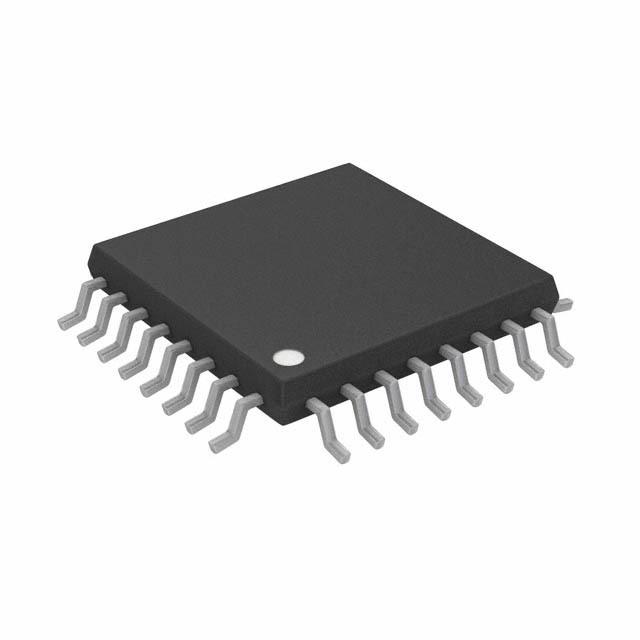
| 描述 | IC DAC 12BIT MICROPWR I2C 6-LLP数模转换器- DAC 12B Micro Pwr DAC |
| 产品分类 | |
| 品牌 | Texas Instruments |
| 产品手册 | |
| 产品图片 |
|
| rohs | 符合RoHS无铅 / 符合限制有害物质指令(RoHS)规范要求 |
| 产品系列 | 数据转换器IC,数模转换器- DAC,Texas Instruments DAC121C081CISD/NOPB- |
| 数据手册 | |
| 产品型号 | DAC121C081CISD/NOPB |
| 产品目录页面 | |
| 产品种类 | 数模转换器- DAC |
| 位数 | 12 |
| 供应商器件封装 | 6-LLP(2.5x2.2) |
| 其它名称 | DAC121C081CISD/NOPBDKR |
| 包装 | Digi-Reel® |
| 商标 | Texas Instruments |
| 安装类型 | 表面贴装 |
| 封装 | Reel |
| 封装/外壳 | 6-WDFN 裸露焊盘 |
| 封装/箱体 | WSON-6 |
| 工作温度 | -40°C ~ 125°C |
| 工厂包装数量 | 1000 |
| 建立时间 | 6µs |
| 数据接口 | I²C |
| 标准包装 | 1 |
| 电压源 | 单电源 |
| 系列 | DAC121C081 |
| 转换器数 | 1 |
| 输出数和类型 | 1 电压,单极1 电压,双极 |
| 配用 | /product-detail/zh/DAC121C08XEB%2FNOPB/DAC121C08XEB%2FNOPB-ND/1785750 |
| 采样率(每秒) | - |


- 商务部:美国ITC正式对集成电路等产品启动337调查
- 曝三星4nm工艺存在良率问题 高通将骁龙8 Gen1或转产台积电
- 太阳诱电将投资9.5亿元在常州建新厂生产MLCC 预计2023年完工
- 英特尔发布欧洲新工厂建设计划 深化IDM 2.0 战略
- 台积电先进制程称霸业界 有大客户加持明年业绩稳了
- 达到5530亿美元!SIA预计今年全球半导体销售额将创下新高
- 英特尔拟将自动驾驶子公司Mobileye上市 估值或超500亿美元
- 三星加码芯片和SET,合并消费电子和移动部门,撤换高东真等 CEO
- 三星电子宣布重大人事变动 还合并消费电子和移动部门
- 海关总署:前11个月进口集成电路产品价值2.52万亿元 增长14.8%


PDF Datasheet 数据手册内容提取
Product Order Technical Tools & Support & Folder Now Documents Software Community DAC121C081,DAC121C085 SNAS395F–DECEMBER2007–REVISEDOCTOBER2016 DAC121C081 and DAC121C085 12-Bit Micro Power Digital-to-Analog Converter With an 2 I C-Compatible Interface 1 Features 2 Applications • EnsuredMonotonicityto12-Bits • IndustrialProcessControl 1 • LowPowerOperation:156-µAMaximumat3.3V • PortableInstruments • ExtendedPowerSupplyRange(2.7Vto5.5V) • DigitalGainandOffsetAdjustment • I2C-Compatible2-WireInterfaceWhichSupports • ProgrammableVoltageandCurrentSources Standard(100-kHz),Fast(400-kHz),andHigh- • TestEquipment Speed(3.4-MHz)Modes • Rail-to-RailVoltageOutput 3 Description • VerySmallPackage The DAC121C081 is a 12-bit, single-channel, voltage-output digital-to-analog converter (DAC) that • Resolution:12bits operates from a 2.7-V to 5.5-V supply. The output • INL:±8LSB(Maximum) amplifier allows rail-to-rail output swing and has an • DNL:0.6/–0.5LSB(Maximum) 8.5-µs settling time. The DAC121C081 uses the • SettlingTime:8.5 µs(Maximum) supply voltage as the reference to provide the widest dynamic output range, and typically consumes 132 • ZeroCodeError:10mV(Maximum) µA while operating at 5 V. It is available in 6-pin SOT • Full-ScaleError:−0.7%FS(Maximum) and WSON packages, and provides three address • SupplyPower options(pinselectable). – Normal:380 µW(3V)/730µW(5V)(Typical) As an alternative, the DAC121C085 provides nine I2C – PowerDown:0.5 µW(3V)/0.9 µW(5V) addressing options and uses an external reference. It has the same performance and settling time as the (Typical) DAC121C081,andisavailableinan8-leadVSSOP. DeviceInformation(1) PARTNUMBER PACKAGE BODYSIZE(NOM) WSON(6) 2.20mm×2.50mm DAC121C081 SOT(6) 1.60mm×2.90mm DAC121C085 VSSOP(8) 3.00mm×3.00mm (1) For all available packages, see the orderable addendum at theendofthedatasheet. BlockDiagram VA* VREF* GND DAC121C081 / DAC121C085 POWER-ON RESET REF REGDIASCTER 12 BIT DAC BUFFER VOUT 12 12 2.5k 100k I2C POCWOENRT-RDOOLWN INTERFACE LOGIC * NOTE: ADR1 and VREF are for the DAC121C085 only. The DAC121C085 uses an external reference (VREF), whereas, the DAC121C081 uses the supply (VA) as the reference. ADR1* ADR0 SCL SDA 1 An IMPORTANT NOTICE at the end of this data sheet addresses availability, warranty, changes, use in safety-critical applications, intellectualpropertymattersandotherimportantdisclaimers.PRODUCTIONDATA.
DAC121C081,DAC121C085 SNAS395F–DECEMBER2007–REVISEDOCTOBER2016 www.ti.com Table of Contents 1 Features.................................................................. 1 8.5 Programming...........................................................20 2 Applications........................................................... 1 8.6 Registers.................................................................21 3 Description............................................................. 1 9 ApplicationandImplementation........................ 22 4 RevisionHistory..................................................... 2 9.1 ApplicationInformation............................................22 9.2 TypicalApplication .................................................24 5 Description(continued)......................................... 3 10 PowerSupplyRecommendations..................... 26 6 PinConfigurationandFunctions......................... 4 10.1 UsingReferencesasPowerSupplies...................26 7 Specifications......................................................... 5 11 Layout................................................................... 29 7.1 AbsoluteMaximumRatings......................................5 11.1 LayoutGuidelines.................................................29 7.2 ESDRatings..............................................................5 11.2 LayoutExample....................................................29 7.3 RecommendedOperatingConditions.......................6 12 DeviceandDocumentationSupport................. 30 7.4 ThermalInformation..................................................6 7.5 ElectricalCharacteristics...........................................7 12.1 DeviceSupport......................................................30 7.6 ACandTimingCharacteristics.................................9 12.2 DocumentationSupport........................................31 7.7 TypicalCharacteristics............................................12 12.3 RelatedLinks........................................................31 12.4 Trademarks...........................................................31 8 DetailedDescription............................................ 15 12.5 ElectrostaticDischargeCaution............................31 8.1 Overview.................................................................15 12.6 Glossary................................................................31 8.2 FunctionalBlockDiagram.......................................15 13 Mechanical,Packaging,andOrderable 8.3 FeatureDescription.................................................15 Information........................................................... 31 8.4 DeviceFunctionalModes........................................20 4 Revision History NOTE:Pagenumbersforpreviousrevisionsmaydifferfrompagenumbersinthecurrentversion. ChangesfromRevisionE(January2016)toRevisionF Page • ChangedV andV descriptions........................................................................................................................................ 4 OUT A • AddedcolumntoTable1. ................................................................................................................................................... 19 ChangesfromRevisionD(March2013)toRevisionE Page • AddedESDRatingstable,FeatureDescriptionsection,DeviceFunctionalModes,ApplicationandImplementation section,PowerSupplyRecommendationssection,Layoutsection,DeviceandDocumentationSupportsection,and Mechanical,Packaging,andOrderableInformationsection. ................................................................................................ 1 • AddedaddressesthattheDACrespondstoontheI2Cbus. ............................................................................................. 18 ChangesfromRevisionC(March2013)toRevisionD Page • ChangedlayoutofNationalSemiconductorDataSheettoTIformat.................................................................................. 29 2 SubmitDocumentationFeedback Copyright©2007–2016,TexasInstrumentsIncorporated ProductFolderLinks:DAC121C081 DAC121C085
DAC121C081,DAC121C085 www.ti.com SNAS395F–DECEMBER2007–REVISEDOCTOBER2016 5 Description (continued) The DAC121C081 and DAC121C085 use a 2-wire, I2C-compatible serial interface that operates in all three speed modes, including high-speed mode (3.4 MHz). An external address selection pin allows up to three DAC121C081 or nine DAC121C085 devices per 2-wire bus. Pin compatible alternatives to the DAC121C081 are availablethatprovideadditionaladdressoptions. The DAC121C081 and DAC121C085 each have a 16-bit register that controls the mode of operation, the power- down condition, and the output voltage. A power-on reset circuit ensures that the DAC output powers up to 0 V. A power-down feature reduces power consumption to less than a microWatt. Their low power consumption and small packages make these DACs an excellent choice for use in battery-operated equipment. Each DAC operatesovertheextendedindustrialtemperaturerangeof −40°Cto+125°C. The DAC121C081 and DAC121C085 are each part of a family of pin compatible DACs that also provide 8 and 10 bit resolution. For 8-bit DACs see the DAC081C081 and DAC081C085. For 10-bit DACs see the DAC101C081andDAC101C085. Copyright©2007–2016,TexasInstrumentsIncorporated SubmitDocumentationFeedback 3 ProductFolderLinks:DAC121C081 DAC121C085
DAC121C081,DAC121C085 SNAS395F–DECEMBER2007–REVISEDOCTOBER2016 www.ti.com 6 Pin Configuration and Functions NGFPackage 6-PinsWSON DDCPackage TopView 6-PinSOT TopView ADR0 1 6 V OUT V 1 6 ADR0 OUT SCL 2 WSON 5 V A V 2 SOT 5 SCL A SDA 3 4 GND GND 3 4 SDA DAC121C081 DAC121C081 DGKPackage 8-PinsVSSOP TopView ADR0 1 8 V OUT ADR1 2 7 V VSSOP REF SCL 3 6 V A SDA 4 5 GND DAC121C085 PinFunctions PIN TYPE DESCRIPTION EQUIVALENTCIRCUIT NAME WSON SOT VSSOP Digital Tri-stateAddressSelectionInput.Setsthetwo ADR0 1 6 1 Input, LeastSignificantBits(A1andA0)ofthe7-bit V+ threelevels slaveaddress.(seeTable1) PIN D1 2.1k 41.5k Digital Snap Tri-stateAddressSelectionInput.SetsBitsA6 Back 41.5k ADR1 — — 2 Input, andA3ofthe7-bitslaveaddress.(seeTable1) threelevels GND GND 4 3 5 Ground Groundforallon-chipcircuitry — SerialClockInput.SCLisusedtogetherwithSDA SCL 2 5 3 DigitalInput tocontrolthetransferofdatainandoutofthe device. PIN SerialDatabi-directionalconnection.Datais Snap D1 Digital clockedintooroutoftheinternal16-bitregister Back SDA 3 4 4 Input/Outpu relativetotheclockedgesofSCL.Thisisan t open-draindatalinethatmustbepulledtothe GND supply(V )byanexternalpullupresistor. A Analog V 6 1 8 AnalogOutputVoltage — OUT Output Powersupplyinput.FortheSOTandWSON V 5 2 6 Supply versions,thissupplyisusedasthereference. — A MustbedecoupledtoGND. Unbufferredreferencevoltage.FortheVSSOP, VREF — — 7 Supply thissupplyisusedasthereference.V must — REF befreeofnoiseanddecoupledtoGND. Exposeddieattachpadcanbeconnectedto groundorleftfloating.Solderingthepadtothe PAD (LLPonly) — — Ground — PCBoffersoptimalthermalperformanceand enhancespackageself-alignmentduringreflow. 4 SubmitDocumentationFeedback Copyright©2007–2016,TexasInstrumentsIncorporated ProductFolderLinks:DAC121C081 DAC121C085
DAC121C081,DAC121C085 www.ti.com SNAS395F–DECEMBER2007–REVISEDOCTOBER2016 7 Specifications 7.1 Absolute Maximum Ratings overoperatingfree-airtemperaturerange(unlessotherwisenoted)(1)(2)(3) MIN MAX UNIT Supplyvoltage,V –0.3 6.5 V A Voltageonanyinputpin –0.3 6.5 V Inputcurrentatanypin(4) ±10 mA Packageinputcurrent(4) ±20 mA PowerconsumptionatT =25°C See(5) A Junctiontemperature,T 150 °C J Storagetemperature,T –65 150 °C stg (1) StressesbeyondthoselistedunderAbsoluteMaximumRatingsmaycausepermanentdamagetothedevice.Thesearestressratings only,whichdonotimplyfunctionaloperationofthedeviceattheseoranyotherconditionsbeyondthoseindicatedunderRecommended OperatingConditions.Exposuretoabsolute-maximum-ratedconditionsforextendedperiodsmayaffectdevicereliability. (2) AllvoltagesaremeasuredwithrespecttoGND=0V,unlessotherwisespecified. (3) IfMilitary/Aerospacespecifieddevicesarerequired,contacttheTexasInstrumentsSalesOffice/Distributorsforavailabilityand specifications. (4) Whentheinputvoltageatanypinexceeds5.5VorislessthanGND,thecurrentatthatpinshouldbelimitedto10mA.The20-mA maximumpackageinputcurrentratingslimitsthenumberofpinsthatcansafelyexceedthepowersupplieswithaninputcurrentof10 mAtotwo. (5) Theabsolutemaximumjunctiontemperature(T )forthisdeviceis150°C.Themaximumallowablepowerdissipationisdictatedby Jmax T ,thejunction-to-ambientthermalresistance(θ ),andtheambienttemperature(T ),andcanbecalculatedusingtheformula Jmax JA A PDMAX=(T −T )/θ .Thevaluesformaximumpowerdissipationwillbereachedonlywhenthedeviceisoperatedinasevere Jmax A JA faultcondition(forexample,wheninputoroutputpinsaredrivenbeyondtheoperatingratings,orthepowersupplypolarityisreversed). 7.2 ESD Ratings VALUE UNIT DAC081C081inNGFPackage Human-bodymodel(HBM),per Allpinsexcept2and3 ±2500 ANSI/ESDA/JEDECJS-001 Pins2and3 ±5000 Charged-devicemodel(CDM),perJEDEC Allpinsexcept2and3 ±1000 V Electrostaticdischarge V (ESD) specificationJESD22-C101 Pins2and3 ±1000 Allpinsexcept2and3 ±250 Machinemodel(MM) Pins2and3 ±350 DAC081C081inDDCPackage Human-bodymodel(HBM),per Allpinsexcept4and5 ±2500 ANSI/ESDA/JEDECJS-001 Pins4and5 ±5000 Charged-devicemodel(CDM),perJEDEC Allpinsexcept4and5 ±1000 V Electrostaticdischarge V (ESD) specificationJESD22-C101 Pins4and5 ±1000 Allpinsexcept4and5 ±250 Machinemodel(MM) Pins4and5 ±350 DAC081C085inDGKPackage Human-bodymodel(HBM),per Allpinsexcept3and4 ±2500 ANSI/ESDA/JEDECJS-001 Pins3and4 ±5000 Charged-devicemodel(CDM),perJEDEC Allpinsexcept3and4 ±1000 V Electrostaticdischarge V (ESD) specificationJESD22-C101 Pins3and4 ±1000 Allpinsexcept3and4 ±250 Machinemodel(MM) Pins3and4 ±350 Copyright©2007–2016,TexasInstrumentsIncorporated SubmitDocumentationFeedback 5 ProductFolderLinks:DAC121C081 DAC121C085
DAC121C081,DAC121C085 SNAS395F–DECEMBER2007–REVISEDOCTOBER2016 www.ti.com 7.3 Recommended Operating Conditions overoperatingfree-airtemperaturerange(unlessotherwisenoted)(1) MIN MAX UNIT Operatingtemperature,T −40 125 °C A Supplyvoltage,V 2.7 5.5 V A Referencevoltage,V 1 V V REFIN A Digitalinputvoltage(2) 0 5.5 V Outputload 0 1500 pF (1) AllvoltagesaremeasuredwithrespecttoGND=0V,unlessotherwisespecified. (2) Theinputsareprotectedasshowninthefollowing.Inputvoltagemagnitudesupto5.5V,regardlessofV ,willnotcauseerrorsinthe A conversionresult.Forexample,ifV is3V,thedigitalinputpinscanbedrivenwitha5-Vlogicdevice. A 7.4 Thermal Information DAC121C081 DAC121C085 THERMALMETRIC(1)(2)(3) NGF(WSON) DDC(SOT) DGK(VSSOP) UNIT 6PINS 6PINS 8PINS R Junction-to-ambientthermalresistance 190 250 240 °C/W θJA (1) Formoreinformationabouttraditionalandnewthermalmetrics,seetheSemiconductorandICPackageThermalMetricsapplication report. (2) SolderingprocessmustcomplywithTexasInstruments'ReflowTemperatureProfileSpecifications,SNOA549. (3) Reflowtemperatureprofilesaredifferentforlead-freepackages. 6 SubmitDocumentationFeedback Copyright©2007–2016,TexasInstrumentsIncorporated ProductFolderLinks:DAC121C081 DAC121C085
DAC121C081,DAC121C085 www.ti.com SNAS395F–DECEMBER2007–REVISEDOCTOBER2016 7.5 Electrical Characteristics ThefollowingspecificationsapplyforV =2.7Vto5.5V,V =V ,C =200pFtoGND,inputcoderange48to4047.All A REF A L MaximumandMinimumlimitsapplyforT ≤T ≤T andallTypicallimitsareatT =25°C,unlessotherwisespecified.(1) MIN A MAX A PARAMETER TESTCONDITIONS MIN TYP(2) MAX(2) UNIT STATICPERFORMANCE Resolution 12 Bits Monotonicity 12 Bits INL 2.2 8 IntegralNon-Linearity LSB –8 –1.5 0.18 0.6 LSB DNL DifferentialNon-Linearity –0.5 –0.12 LSB ZE ZeroCodeError I =0 1.1 10 mV OUT FSE Full-ScaleError I =0 –0.1 −0.7 %FSR OUT GE GainError AllonesLoadedtoDACregister –0.2 −0.7 %FSR ZCED ZeroCodeErrorDrift –20 µV/°C VA=3V –0.7 ppm TCGE GainErrorTempco V =5V –1 FSR/°C A ANALOGOUTPUTCHARACTERISTICS(V ) OUT DAC121C085 0 V Outputvoltagerange(3) REF V DAC121C081 0 V A V =3V,I =200µA 1.3 A OUT ZCO Zerocodeoutput mV V =5V,I =200µA 7 A OUT V =3V,I =200µA 2.984 A OUT FSO Fullscaleoutput V V =5V,I =200µA 4.989 A OUT V =3V,V =0V, A OUT 56 Outputshort-circuitcurrent InputCode=FFFh. I mA OS (ISOURCE) VA=5V,VOUT=0V, 69 InputCode=FFFh. V =3V,V =3V, A OUT –52 Outputshort-circuitcurrent InputCode=000h. I mA OS (ISINK) VA=5V,VOUT=5V, –75 InputCode=000h. I Continuousoutputcurrent(3) AvailableontheDACoutput 11 mA O R =∞ 1500 L C Maximumloadcapacitance pF L R =2kΩ 1500 L Z DCoutputimpedance 7.5 Ω OUT REFERENCEINPUTCHARACTERISTICS(DAC121C085only) Inputrangeminimum 1 0.2 V V Inputrangemaximum V V REF A Inputimpedance 120 kΩ LOGICINPUTCHARACTERISTICS(SCL,SDA) V Inputhighvoltage 0.7×V V IH A V Inputlowvoltage 0.3×V V IL A I Inputcurrent ±1 µA IN C Inputpincapacitance(3) 3 pF IN V Inputhysteresis 0.1×V V HYST A LOGICINPUTCHARACTERISTICS(ADR0,ADR1) V Inputhighvoltage V -0.5 V IH A (1) Valuesshowninthistablearedesigntargetsandaresubjecttochangebeforeproductrelease. (2) TypicalfiguresareatT =25°C,andrepresentmostlikelyparametricnorms.TestlimitsarespecifiedtoAOQL(AverageOutgoing J QualityLevel). (3) Thisparameterisspecifiedbydesignand/orcharacterizationandisnottestedinproduction. Copyright©2007–2016,TexasInstrumentsIncorporated SubmitDocumentationFeedback 7 ProductFolderLinks:DAC121C081 DAC121C085
DAC121C081,DAC121C085 SNAS395F–DECEMBER2007–REVISEDOCTOBER2016 www.ti.com Electrical Characteristics (continued) ThefollowingspecificationsapplyforV =2.7Vto5.5V,V =V ,C =200pFtoGND,inputcoderange48to4047.All A REF A L MaximumandMinimumlimitsapplyforT ≤T ≤T andallTypicallimitsareatT =25°C,unlessotherwisespecified.(1) MIN A MAX A PARAMETER TESTCONDITIONS MIN TYP(2) MAX(2) UNIT V Inputlowvoltage 0.5 V IL I Inputcurrent ±1 µA IN LOGICOUTPUTCHARACTERISTICS(SDA) I =3mA 0.4 SINK V Outputlowvoltage V OL I =6mA 0.6 SINK High-impedenceoutputleakage I ±1 µA OZ current POWERREQUIREMENTS Supplyvoltageminimum 2.7 V V A Supplyvoltagemaximum 5.5 Normal--V settomidscale.2-wireinterfacequiet(SCL=SDA=V ).(outputunloaded) OUT A V =2.7Vto3.6V 105 156 A I V DAC121C081supplycurrent µA ST_VA-1 A V =4.5Vto5.5V 132 214 A V =2.7Vto3.6V 86 118 A I V DAC121C085supplycurrent µA ST_VA-5 A V =4.5Vto5.5V 98 152 A I VREFsupplycurrent VA=2.7Vto3.6V 37 43 µA ST_VREF (DAC121C085only) V =4.5Vto5.5V 53 61 A Powerconsumption V =3V 380 A P (V andV for µW ST A REF DAC121C085)(4) VA=5V 730 ContinuousOperation--2-wireinterfaceactivelyaddressingtheDACandwritingtotheDACregister.(outputunloaded) V =2.7Vto3.6V 134 220 A f =400kHz µA SCL V =4.5Vto5.5V 192 300 A I V DAC121C081supplycurrent CO_VA-1 A V =2.7Vto3.6V 225 320 A f =3.4MHz µA SCL V =4.5Vto5.5V 374 500 A V =2.7Vto3.6V 101 155 A f =400kHz µA SCL V =4.5Vto5.5V 142 220 A I V DAC121C085supplycurrent CO_VA-5 A V =2.7Vto3.6V 193 235 A f =3.4MHz µA SCL V =4.5Vto5.5V 325 410 A I VREFsupplycurrent VA=2.7Vto3.6V 33.5 55 µA CO_VREF (DAC121C085only) V =4.5Vto5.5V 49.5 71.4 A V =3V 480 µW A f =400kHz SCL Powerconsumption VA=5V 1.06 mW P CO (VAandVREFforDAC121C085) VA=3V 810 µW f =3.4MHz SCL V =5V 2.06 mW A PowerDown--2-wireinterfacequiet(SCL=SDA=V )afterPDmodewrittentoDACregister.(outputunloaded) A Supplycurrent Allpower-down VA=2.7Vto3.6 0.13 1.52 I µA PD (VAandVREFforDAC121C085) modes VA=4.5Vto5.5V 0.15 3.25 Powerconsumption Allpower-down VA=3V 0.5 P µW PD (VAandVREFforDAC121C085) modes VA=5V 0.9 (4) Toensureaccuracy,itisrequiredthatV andV bewellbypassed. A REF 8 SubmitDocumentationFeedback Copyright©2007–2016,TexasInstrumentsIncorporated ProductFolderLinks:DAC121C081 DAC121C085
DAC121C081,DAC121C085 www.ti.com SNAS395F–DECEMBER2007–REVISEDOCTOBER2016 7.6 AC and Timing Characteristics ThefollowingspecificationsapplyforV =2.7Vto5.5V,V =V ,R =Infinity,C =200pFtoGND.AllMaximumand A REF A L L MinimumlimitsapplyforT ≤T ≤T andallTypicallimitsareatT =25°C,unlessotherwisespecified.(1) MIN A MAX A PARAMETER TESTCONDITIONS(2) MIN TYP(3) MAX(2)(3) UNIT t OutputVoltageSettlingTime(4) 400htoC00hcodechange 6 8.5 µs s R =2kΩ,C =200pF L L SR OutputSlewRate 1 V/µs GlitchImpulse Codechangefrom800hto7FFh 12 nV-sec DigitalFeedthrough 0.5 nV-sec MultiplyingBandwidth(5) V =2.5V±0.1Vpp 160 kHz REF TotalHarmonicDistortion(5) VREF=2.5V±0.1Vpp 70 dB inputfrequency=10kHz V =3V 0.8 µs A t Wake-UpTime WU V =5V 0.5 µs A DIGITALTIMINGSPECS(SCL,SDA) StandardMode 100 kHz FastMode 400 f SerialClockFrequency SCL HighSpeedMode,C =100pF 3.4 b MHz HighSpeedMode,C =400pF 1.7 b StandardMode 4.7 µs FastMode 1.3 t SCLLowTime LOW HighSpeedMode,C =100pF 160 b ns HighSpeedMode,C =400pF 320 b StandardMode 4 µs FastMode 0.6 t SCLHighTime HIGH HighSpeedMode,C =100pF 60 b ns HighSpeedMode,C =400pF 120 b StandardMode 250 t DataSetupTime FastMode 100 ns SU;DAT HighSpeedMode 10 StandardMode 0 3.45 µs FastMode 0 0.9 t DataHoldTime HD;DAT HighSpeedMode,C =100pF 0 70 b ns HighSpeedMode,C =400pF 0 150 b StandardMode 4.7 Setuptimeforastartora µs t FastMode 0.6 SU;STA repeatedstartcondition HighSpeedMode 160 ns StandardMode 4 Holdtimeforastartora µs t FastMode 0.6 HD;STA repeatedstartcondition HighSpeedMode 160 ns Busfreetimebetweenastop StandardMode 4.7 t µs BUF andstartcondition FastMode 1.3 StandardMode 4 µs t Setuptimeforastopcondition FastMode 0.6 SU;STO HighSpeedMode 160 ns (1) Valuesshowninthistablearedesigntargetsandaresubjecttochangebeforeproductrelease. (2) C referstothecapacitanceofonebusline.C isexpressedinpFunits. b b (3) TypicalfiguresareatT =25°C,andrepresentmostlikelyparametricnorms.TestlimitsarespecifiedtoAOQL(AverageOutgoing J QualityLevel). (4) Thisparameterisspecifiedbydesignand/orcharacterizationandisnottestedinproduction. (5) AppliestotheMultiplyingDACconfiguration.Inthisconfiguration,thereferenceisusedastheanaloginput.Thevalueloadedinthe DACRegisterwilldigitallyattenuatethesignalatVout. Copyright©2007–2016,TexasInstrumentsIncorporated SubmitDocumentationFeedback 9 ProductFolderLinks:DAC121C081 DAC121C085
DAC121C081,DAC121C085 SNAS395F–DECEMBER2007–REVISEDOCTOBER2016 www.ti.com AC and Timing Characteristics (continued) ThefollowingspecificationsapplyforV =2.7Vto5.5V,V =V ,R =Infinity,C =200pFtoGND.AllMaximumand A REF A L L MinimumlimitsapplyforT ≤T ≤T andallTypicallimitsareatT =25°C,unlessotherwisespecified.(1) MIN A MAX A PARAMETER TESTCONDITIONS(2) MIN TYP(3) MAX(2)(3) UNIT StandardMode 1000 FastMode 20+0.1C 300 b t RisetimeofSDAsignal ns rDA HighSpeedMode,C =100pF 10 80 b HighSpeedMode,C =400pF 20 160 b StandardMode 250 FastMode 20+0.1C 250 b t FalltimeofSDAsignal ns fDA HighSpeedMode,C =100pF 10 80 b HighSpeedMode,C =400pF 20 160 b StandardMode 1000 FastMode 20+0.1C 300 b t RisetimeofSCLsignal ns rCL HighSpeedMode,C =100pF 10 40 b HighSpeedMode,C =400pF 20 80 b StandardMode 1000 RisetimeofSCLsignalaftera FastMode 20+0.1C 300 b t repeatedstartconditionandafter ns rCL1 anacknowledgebit. HighSpeedMode,Cb=100pF 10 80 HighSpeedMode,C =400pF 20 160 b StandardMode 300 FastMode 20+0.1C 300 b t FalltimeofaSCLsignal ns fCL HighSpeedMode,C =100pF 10 40 b HighSpeedMode,C =400pF 20 80 b Capacitiveloadforeachbusline C 400 pF b (SCLandSDA) PulseWidthofspike FastMode 50 tSP suppressed(6)(4) HighSpeedMode 10 ns SDAoutputdelay(seethe FastMode 87 270 t AdditionalTimingInformation ns outz section) HighSpeedMode 38 60 (6) SpikesuppressionfilteringonSCLandSDAwillsupressspikesthatarelessthan50nsforstandard-fastmodeandlessthan10nsfor hs-mode. 10 SubmitDocumentationFeedback Copyright©2007–2016,TexasInstrumentsIncorporated ProductFolderLinks:DAC121C081 DAC121C085
DAC121C081,DAC121C085 www.ti.com SNAS395F–DECEMBER2007–REVISEDOCTOBER2016 FSE 4095 x VREF 4096 GE = FSE - ZE FSE = GE + ZE OUTPUT VOLTAGE ZE 0 0 4095 DIGITAL INPUT CODE Figure1. Input/OutputTransferCharacteristic SDA tf tLOW tHD;STA tr tBUF tr tf tSP SCL tHD;STA tSU;STA tSU;STO tHIGH tHD;DAT tSU;DAT START REPEATED STOP START START Figure2. SerialTimingDiagram Copyright©2007–2016,TexasInstrumentsIncorporated SubmitDocumentationFeedback 11 ProductFolderLinks:DAC121C081 DAC121C085
DAC121C081,DAC121C085 SNAS395F–DECEMBER2007–REVISEDOCTOBER2016 www.ti.com 7.7 Typical Characteristics V =V ,f =3.4MHz,T =25°C,InputCodeRange48to4047,unlessotherwisestated. REF A SCL A Figure3.INL Figure4.DNL Figure5.INL/DNLvsTemperatureatV =3V Figure6.INL/DNLvsTemperatureatV =5V A A Figure7.INL/DNLvsV atV =3V Figure8.INL/DNLvsV atV =5V REFIN A REFIN A 12 SubmitDocumentationFeedback Copyright©2007–2016,TexasInstrumentsIncorporated ProductFolderLinks:DAC121C081 DAC121C085
DAC121C081,DAC121C085 www.ti.com SNAS395F–DECEMBER2007–REVISEDOCTOBER2016 Typical Characteristics (continued) V =V ,f =3.4MHz,T =25°C,InputCodeRange48to4047,unlessotherwisestated. REF A SCL A Figure9.INL/DNLvsV Figure10.ZeroCodeErrorvsV A A Figure11.ZeroCodeErrorvsTemperature Figure12.FullScaleErrorvsV A Figure13.FullScaleErrorvsTemperature Figure14.TotalSupplyCurrentvsV A Copyright©2007–2016,TexasInstrumentsIncorporated SubmitDocumentationFeedback 13 ProductFolderLinks:DAC121C081 DAC121C085
DAC121C081,DAC121C085 SNAS395F–DECEMBER2007–REVISEDOCTOBER2016 www.ti.com Typical Characteristics (continued) V =V ,f =3.4MHz,T =25°C,InputCodeRange48to4047,unlessotherwisestated. REF A SCL A Figure15.VREFSupplyCurrentvsVA Figure16.TotalSupplyCurrentvsTemperatureatVA=3V Figure17.TotalSupplyCurrentvsTemperatureatV =5V Figure18.5-VGlitchResponse A Figure19.Power-OnReset 14 SubmitDocumentationFeedback Copyright©2007–2016,TexasInstrumentsIncorporated ProductFolderLinks:DAC121C081 DAC121C085
DAC121C081,DAC121C085 www.ti.com SNAS395F–DECEMBER2007–REVISEDOCTOBER2016 8 Detailed Description 8.1 Overview The DAC121C081 is fabricated on a CMOS process with an architecture that consists of switches and resistor stringsthatarefollowedbyanoutputbuffer. 8.2 Functional Block Diagram VA* VREF* GND DAC121C081 / DAC121C085 POWER-ON RESET REF REGDIASCTER 12 BIT DAC BUFFER VOUT 12 12 2.5k 100k I2C POCWOENRT-RDOOLWN INTERFACE LOGIC * NOTE: ADR1 and VREF are for the DAC121C085 only. The DAC121C085 uses an external reference (VREF), whereas, the DAC121C081 uses the supply (VA) as the reference. ADR1* ADR0 SCL SDA 8.3 Feature Description 8.3.1 DACSection The DAC121C081 is fabricated on a CMOS process with an architecture that consists of switches and resistor stringsthatarefollowedbyanoutputbuffer. For simplicity, a single resistor string is shown in Figure 20. This string consists of 4096 equal valued resistors with a switch at each junction of two resistors, plus a switch to ground. The code loaded into the DAC register determines which switch is closed, connecting the proper node to the amplifier. The input coding is straight binarywithanidealoutputvoltageof: V =V ×(D/4096) OUT REF whereDisthedecimalequivalentofthebinarycodethatisloadedintotheDACregister. (1) Dcantakeonanyintegervaluefrom0to4095.ThisconfigurationensuresthattheDACismonotonic. Copyright©2007–2016,TexasInstrumentsIncorporated SubmitDocumentationFeedback 15 ProductFolderLinks:DAC121C081 DAC121C085
DAC121C081,DAC121C085 SNAS395F–DECEMBER2007–REVISEDOCTOBER2016 www.ti.com Feature Description (continued) VREF R R R To Output Amplifier R R Figure20. DACResistorString 8.3.2 OutputAmplifier The output amplifier is rail-to-rail, providing an output voltage range of 0 V to V when the reference is V . All A A amplifiers, even rail-to-rail types, exhibit a loss of linearity as the output approaches the supply rails (0 V and V , A inthiscase).Forthisreason,linearityisspecifiedoverlessthanthefulloutputrangeoftheDAC.However,ifthe reference is less than V , there is only a loss in linearity in the lowest codes. The output capabilities of the A amplifieraredescribedintheElectricalCharacteristics. The output amplifiers are capable of driving a load of 2 kΩ in parallel with 1500 pF to ground or to V . The zero- A codeandfull-scaleoutputsforgivenloadcurrentsareavailableintheElectricalCharacteristics. 8.3.3 ReferenceVoltage The DAC121C081 uses the supply (V ) as the reference. With that said, V must be treated as a reference. The A A analog output is only as clean as the reference (V ). TI recommends driving the reference with a voltage source A withlow-outputimpedance. The DAC121C085 comes with an external reference supply pin (V ). For the DAC121C085, it is important that REF V bekeptascleanaspossible. REF Applications Information describes a handful of ways to drive the reference appropriately. See Using References asPowerSuppliesfordetails. 16 SubmitDocumentationFeedback Copyright©2007–2016,TexasInstrumentsIncorporated ProductFolderLinks:DAC121C081 DAC121C085
DAC121C081,DAC121C085 www.ti.com SNAS395F–DECEMBER2007–REVISEDOCTOBER2016 Feature Description (continued) 8.3.4 SerialInterface The I2C-compatible interface operates in all three speed modes. Standard mode (100 kHz) and Fast mode (400 kHz) are functionally the same and will be referred to as Standard-Fast mode in this document. High-Speed mode (3.4MHz) is an extension of Standard-Fast mode and will be referred to as Hs-mode in this document. The following diagrams describe the timing relationships of the clock (SCL) and data (SDA) signals. Pullup resistors or current sources are required on the SCL and SDA busses to pull them high when they are not being driven low. A logic zero is transmitted by driving the output low. A logic high is transmitted by releasing the output and allowingittobepulledupexternally.Theappropriatepullupresistorvaluesdependsonthetotalbuscapacitance andoperatingspeed. 8.3.4.1 BasicI2CProtocol The I2C interface is bi-directional and allows multiple devices to operate on the same bus. To facilitate this bus configuration, each device has a unique hardware address which is referred to as the slave address. To communicate with a particular device on the bus, the controller (master) sends the slave address and listens for aresponsefromtheslave.Thisresponseisreferredtoasanacknowledgebit.Ifaslaveonthebusisaddressed correctly, it Acknowledges (ACKs) the master by driving the SDA bus low. If the address doesn't match a device's slave address, it Not-acknowledges (NACKs) the master by letting SDA be pulled high. ACKs also occur onthebuswhendataisbeingtransmitted.Whenthemasteriswritingdata,theslaveACKsaftereverydatabyte is successfully received. When the master is reading data, the master ACKs after every data byte is received to let the slave know it wants to receive another data byte. When the master wants to stop reading, it NACKs after thelastdatabyteandcreatesaStopconditiononthebus. All communication on the bus begins with either a Start condition or a Repeated Start condition. The protocol for starting the bus varies between Standard-Fast mode and Hs-mode. In Standard-Fast mode, the master generates a Start condition by driving SDA from high to low while SCL is high. In Hs-mode, starting the bus is more complicated. See High-Speed (Hs) Mode for the full details of a Hs-mode Start condition. A Repeated Start isgeneratedtoeitheraddressadifferentdevice,orswitchbetweenreadandwritemodes.Themastergenerates a Repeated Start condition by driving SDA low while SCL is high. Following the Repeated Start, the master sends out the slave address and a read/write bit as shown in Figure 21. The bus continues to operate in the samespeedmodeasbeforetheRepeatedStartcondition. All communication on the bus ends with a Stop condition. In either Standard-Fast mode or Hs-Mode, a Stop condition occurs when SDA is pulled from low to high while SCL is high. After a Stop condition, the bus remains idleuntilamastergeneratesaStartcondition. SeethePhillipsI2C®Specification(Version2.1Jan,2000)foradetaileddescriptionoftheserialinterface. SDA MSB LSB ACK MSB LSB N/ACK R/W 7-bit Slave Address Direction Data Byte Bit Acknowledge *Acknowledge from the Device or Not-ACK SCL 1 2 6 7 8 9 1 2 8 9 START or Repeated for the Lower Data Byte STOP REPEATED and Additional Data Transfers START *Note: In continuous mode, this bit must be an ACK from the data receiver. Immediately preceding a STOP condition, this bit must be a NACK from the master. Figure21. BasicOperation Copyright©2007–2016,TexasInstrumentsIncorporated SubmitDocumentationFeedback 17 ProductFolderLinks:DAC121C081 DAC121C085
DAC121C081,DAC121C085 SNAS395F–DECEMBER2007–REVISEDOCTOBER2016 www.ti.com Feature Description (continued) 8.3.4.2 Standard-FastMode In Standard-Fast mode, the master generates a start condition by driving SDA from high to low while SCL is high. The Start condition is always followed by a 7-bit slave address and a Read/Write bit. After these eight bits have been transmitted by the master, SDA is released by the master and the DAC121C081 either ACKs or NACKs the address. If the slave address matches, the DAC121C081 ACKs the master. If the address doesn't match,theDAC121C081NACKsthemaster. For a write operation, the master follows the ACK by sending the upper eight data bits to the DAC121C081. Then the DAC121C081 ACKs the transfer by driving SDA low. Next, the lower eight data bits are sent by the master. The DAC121C081 then ACKs the transfer. At this point, the DAC output updates to reflect the contents of the 16-bit DAC register. Next, the master either sends another pair of data bytes, generates a Stop condition toendcommunication,orgeneratesaRepeatedStartconditiontocommunicatewithanotherdeviceonthebus. For a read operation, the DAC121C081 sends out the upper eight data bits of the DAC register. This is followed by an ACK by the master. Next, the lower eight data bits of the DAC register are sent to the master. The master then produces a NACK by letting SDA be pulled high. The NACK is followed by a master-generated Stop conditiontoendcommunicationonthebus,oraRepeatedStarttocommunicatewithanotherdeviceonthebus. 8.3.4.3 High-Speed(Hs)Mode For Hs-mode, the sequence of events to begin communication differ slightly from Standard-Fast mode. Figure 22 describes this in further detail. Initially, the bus begins running in Standard-Fast mode. The master generates a Start condition and sends the 8-bit Hs master code (00001XXX) to the DAC121C081. Next, the DAC121C081 responds with a NACK. Once the SCL line has been pulled to a high level, the master switches to Hs-mode by increasing the bus speed and generating a Repeated Start condition (driving SDA low while SCL is pulled high). At this point, the master sends the slave address to the DAC121C081, and communication continues as shown inFigure21. When the master generates a Repeated Start condition while in Hs-mode, the bus stays in Hs-mode awaiting the slave address from the master. The bus continues to run in Hs-mode until a Stop condition is generated by the master. When the master generates a Stop condition on the bus, the bus must be started in Standard-Fast mode againbeforeincreasingthebusspeedandswitchingtoHs-mode.ns16705 SDA NACK MSB 8-ELW(cid:3)0DVWHU(cid:3)FRGH(cid:3)‡00001[[[· 7-bit Slave Address Not-Acknowledge from the Device SCL 1 2 5 6 7 8 9 1 2 Repeated START START Standard-Fast Mode Hs-Mode Figure22. BeginningHs-ModeCommunication 8.3.4.4 I2CSlave(Hardware)Address The DAC has a seven-bit I2C slave address. For the VSSOP version of the DAC, this address is configured by the ADR0 and ADR1 address selection inputs. For the DAC121C081, the address is configured by the ADR0 address selection input. ADR0 and ADR1 can be grounded, left floating, or tied to V . If desired, the address A selection inputs can be set to V /2 rather than left floating. The state of these inputs sets the address the DAC A responds to on the I2C bus (see Table 1). In addition to the selectable slave address, there is also a broadcast address (1001000) for all DAC121C081's and DAC121C085's on the 2-wire bus. When the bus is addressed by the broadcast address, all the DAC121C081's and DAC121C085's will respond and update synchronously. Figure 24 and Figure 25 describe how the master device should address the DAC through the I2C-Compatible interface. 18 SubmitDocumentationFeedback Copyright©2007–2016,TexasInstrumentsIncorporated ProductFolderLinks:DAC121C081 DAC121C085
DAC121C081,DAC121C085 www.ti.com SNAS395F–DECEMBER2007–REVISEDOCTOBER2016 Feature Description (continued) Keep in mind that the address selection inputs (ADR0 and ADR1) are only sampled until the DAC is correctly addressed with a non-broadcast address. At this point, the ADR0 and ADR1 inputs TRI-STATE and the slave address is locked. Changes to ADR0 and ADR1 will not update the selected slave address until the device is power-cycled. Table1.SlaveAddresses DAC121C081(SOT SlaveAddress DAC121C085(VSSOP) ANDWSON)(1) DoNotUse(2) [A6-A0] ADR1 ADR0 ADR0 0001100 Floating Floating Floating 1000110 0001101 Floating GND GND 1000110 0001110 Floating V V 1000111 A A 0001000 GND Floating --------------- 1000100 0001001 GND GND --------------- 1000100 0001010 GND V --------------- 1000101 A 1001100 V Floating --------------- 1100110 A 1001101 V GND --------------- 1100110 A 1001110 V V --------------- 1100111 A A 1001000 ---------------BroadcastAddress--------------- 1100100 (1) Pin-compatiblealternativestotheDAC121C081optionsareavailablewithadditionaladdressoptions. (2) TheseaddressesshouldnotbeusedbyotherI2CdevicesontheI2Cbus.UsingtheseaddressescancausetheDAC121C081/085to notrespondwhenaddressedbytheassignedSlaveAddress. 8.3.5 Power-OnReset The power-on reset circuit controls the output voltage of the DAC during power up. Upon application of power, the DAC register is filled with zeros and the output voltage is 0 V. The output remains at 0 V until a valid write sequenceismadetotheDAC. When resetting the device, it is crutial that the V supply be lowered to a maximum of 200 mV before the supply A is raised again to power up the device. Dropping the supply to within 200 mV of GND during a reset will ensure theADCperformsasspecified. 8.3.6 SimultaneousReset The broadcast address allows the I2C master to write a single word to multiple DACs simultaneously. Provided that all of the DACs exist on a single I2C bus, every DAC updates when the broadcast address is used to address the bus. This feature allows the master to reset all of the DACs on a shared I2C bus to a specific digital code. For instance, if the master writes a power-down code to the bus with the broadcast address, all of the DACspowersdownsimultaneously. 8.3.7 AdditionalTimingInformation:t outz The t specification is provided to aid the design of the I2C bus. After the SCL bus is driven low by the I2C outz master, the SDA bus will be held for a short time by the DAC121C081. This time is referred to as t . The outz following figure illustrates the relationship between the fall of SCL, at the 30% threshold, to the time when the DAC begins to transition the SDA bus. The t specification only applies when the DAC is in control of the SDA outz bus. The DAC is only in control of the bus during an ACK by the DAC121C081 or a data byte read from the DAC (seeFigure25). Copyright©2007–2016,TexasInstrumentsIncorporated SubmitDocumentationFeedback 19 ProductFolderLinks:DAC121C081 DAC121C085
DAC121C081,DAC121C085 SNAS395F–DECEMBER2007–REVISEDOCTOBER2016 www.ti.com SCL SDA toutz Figure23. DataOutputTiming Thet specificationistypically87nsinStandard-FastModeand38nsinHs-Mode. outz 8.4 Device Functional Modes 8.4.1 Power-DownModes The DAC121C081 has three power-down modes. In power-down mode, the supply current drops to 0.13 µA at 3 V and 0.15 µA at 5 V (typical). The DAC121C081 is put into power-down mode by writing a one to PD1 and/or PD0. The outputs can be set to high impedance, terminated by 2.5 kΩ to GND, or terminated by 100 kΩ to GND (seeFigure26). The bias generator, output amplifier, resistor string, and other linear circuitry are all shut down in any of the power-down modes. When the DAC121C081 is powered down, the value written to the DAC register, including the power-down bits, is saved. While the DAC is in power-down, the saved DAC register contents can be read back.WhentheDACisbroughtoutofpower-downmode,theDACregistercontentswillbeoverwrittenandV OUT willbeupdatedwiththenew12-bitdatavalue. Thetimetoexitpower-down(Wake-UpTime)istypically0.8 µsat3Vand0.5 µsat5V. 8.5 Programming 8.5.1 WritingtotheDACRegister To write to the DAC, the master addresses the part with the correct slave address (A6-A0) and writes a zero to the read/write bit. If addressed correctly, the DAC returns an ACK to the master. The master then sends out the upper data byte. The DAC responds by sending an ACK to the master. Next, the master sends the lower data byte to the DAC. The DAC responds by sending an ACK again. At this point, the master either sends the upper byte of the next data word to be converted by the DAC, generates a Stop condition to end communication, or generates a Repeated Start condition to begin communication with another device on the bus. Until generating a Stop condition, the master can continuously write the upper and lower data bytes to the DAC register. This allowsforamaximumDACconversionrateof188.9kilo-conversionspersecondinHs-mode. 1 9 1 9 1 9 SCL SDA A6 A5 A4 A3 A2 A1 A0 R/W 0 0 PD1PD0 D11 D10 D9 D8 D7 D6 D5 D4 D3 D2 D1 D0 Start by ACK ACK ACK Stop by Master by by by Master Frame 1 DAC121C081 Frame 2 DAC121C081 Frame 3 DAC121C081 Address Byte Data Byte from Data Byte from from Master Master Master Repeat Frames 2 & 3 for Continuous Mode Figure24. TypicalWritetotheDACRegister 20 SubmitDocumentationFeedback Copyright©2007–2016,TexasInstrumentsIncorporated ProductFolderLinks:DAC121C081 DAC121C085
DAC121C081,DAC121C085 www.ti.com SNAS395F–DECEMBER2007–REVISEDOCTOBER2016 Programming (continued) 8.5.2 ReadingfromtheDACRegister To read from the DAC register, the master addresses the part with the correct slave address (A6-A0) and writes a one to the read/write bit. If addressed correctly, the DAC returns an ACK to the master. Next, the DAC sends out the upper data byte. The master responds by sending an ACK to the DAC to indicate that it wants to receive anotherdatabyte.ThentheDACsendsthelowerdatabytetothemaster.Assumingonlyone16-bitdatawordis read, the master sends a NACK after receiving the lower data byte. At this point, the master either generates a Stop condition to end communication, or a Repeated Start condition to begin communication with another device onthebus. 1 9 1 9 1 9 SCL SDA A6 A5 A4 A3 A2 A1 A0 R/W 0 0 PD1PD0 D11 D10 D9 D8 D7 D6 D5 D4 D3 D2 D1 D0 Start by ACK ACK NACK Stop by Master by by by Master Frame 1 DAC121C081 Frame 2 Master Frame 3 Master Address Byte Data Byte from Data Byte from from Master DAC121C081 DAC121C081 Figure25. TypicalReadfromtheDACRegister 8.6 Registers 8.6.1 DACRegister The DAC register, Figure 26, has sixteen bits. The first two bits are always zero. The next two bits determine the mode of operation (normal mode or one of three power-down modes). The final twelve bits of the shift register are the data bits. The data format is straight binary (MSB first, LSB last), with twelve 0s corresponding to an output of 0 V and twelve 1s corresponding to a full-scale output of V – 1 LSB. When writing to the DAC A Register,V willupdateontherisingedgeoftheACKfollowingthelowerdatabyte. OUT MSB LSB X X PD1PD0D11D10 D9 D8 D7 D6 D5 D4 D3 D2 D1 D0 DATA BITS 0 0 Normal Operation. 0 1 2.5k(cid:214) to GND. 1 0 100k(cid:214) to GND. Power-Down Modes 1 1 High Impedance. Figure26. DACRegisterContents Copyright©2007–2016,TexasInstrumentsIncorporated SubmitDocumentationFeedback 21 ProductFolderLinks:DAC121C081 DAC121C085
DAC121C081,DAC121C085 SNAS395F–DECEMBER2007–REVISEDOCTOBER2016 www.ti.com 9 Application and Implementation NOTE Information in the following applications sections is not part of the TI component specification, and TI does not warrant its accuracy or completeness. TI’s customers are responsible for determining suitability of components for their purposes. Customers should validateandtesttheirdesignimplementationtoconfirmsystemfunctionality. 9.1 Application Information 9.1.1 BipolarOperation The DAC121C081 is designed for single supply operation and thus has a unipolar output. However, a bipolar output may be obtained with the circuit in Figure 27. This circuit provides an output voltage range of ±5 V. A rail- to-railamplifiershouldbeusediftheamplifiersuppliesarelimitedto±5V. 10 pF R2 +5V +5V R1 10 PF + 0.1 PF - ±5V + DAC121C081 -5V SDA VOUT SCL Figure27. BipolarOperation Theoutputvoltageofthiscircuitforanycodeisfoundtobe,asshowninEquation2: V =(V ×(D/4096)×((R1+R2)/R1)–V ×R2/R1) O A A whereDistheinputcodeindecimalform. (2) Equation3showsthatwithV =5VandR1=R2, A V =(10×D/4096)–5V (3) O Alistofrail-to-railamplifierssuitableforthisapplicationareindicatedinTable2. Table2.SomeRail-to-RailAmplifiers AMP PKGS TypV TypI OS SUPPLY LMP7701 SOT-23 37uV 0.79mA LMV841 SC70-5 50uV 1mA LMC7111 SOT-23 0.9mV 25µA LM7301 SO-8,SOT-23 0.03mV 620µA LM8261 SOT-23 0.7mV 1mA 22 SubmitDocumentationFeedback Copyright©2007–2016,TexasInstrumentsIncorporated ProductFolderLinks:DAC121C081 DAC121C085
DAC121C081,DAC121C085 www.ti.com SNAS395F–DECEMBER2007–REVISEDOCTOBER2016 9.1.2 DSP/MicroprocessorInterfacing Interfacing the DAC121C081 to microprocessors and DSPs is quite simple. The following guidelines are offered tosimplifythedesignprocess. 9.1.2.1 Interfacingtothe2-wireBus Figure 28 shows a microcontroller interfacing to the DAC121C081 through the 2-wire bus. Pullup resistors (Rp) should be chosen to create an appropriate bus rise time and to limit the current that will be sunk by the open- drainoutputsofthedevicesonthebus.SeetheI2C®Specificationforfurtherdetails.Typicalpullupvaluestouse in Standard-Fast mode bus applications are 2 kΩ to 10 kΩ. SCL and SDA series resisters (R ) near the S DAC121C081areoptional.Ifhigh-voltagespikesareexpectedonthe2-wirebus,seriesresistorsshouldbeused to filter the voltage on SDA and SCL. The value of the series resistance must be picked to ensure the V IL thresholdcanbeachieved.Ifused,R istypically51 Ω. S Regulated Supply F F F VA VREF 0.1 P 4.7 P 10 P VDD DAC121C081/5 RP RP uController RS* SDA SDA SCL SCL RS* ADC121C021 SDA SCL I2C Device SDA SCL *NOTE: RS is optional. Figure28. SerialInterfaceConnectionDiagram 9.1.2.2 InterfacingtoaHs-modeBus Interfacing to a Hs-mode bus is very similar to interfacing to a Standard-Fast mode bus. In Hs-mode, the specified rise time of SCL is shortened. To create a faster rise time, the master device (microcontroller) can drive the SCL bus high and low. In other words, the microcontroller can drive the line high rather than leaving it to the pullup resistor. It is also possible to decrease the value of the pullup resistors or increase the pullup current to meetthetightertimingspecs.SeetheI2C®Specificationforfurtherdetails. Copyright©2007–2016,TexasInstrumentsIncorporated SubmitDocumentationFeedback 23 ProductFolderLinks:DAC121C081 DAC121C085
DAC121C081,DAC121C085 SNAS395F–DECEMBER2007–REVISEDOCTOBER2016 www.ti.com 9.2 Typical Application 2 VA 4 SDA 1 5 SCL VOUT DAC121C081CIMK 6 ADR0 +5 LM4132-3.3 120pF 4 3 5 +5 3 2 .1uF 1uF 3 + 5 1 A2 4 - 2 .2uF 180 +5 +3.3 100K 1 10 9 470pF 2 VREF VA VIO 8 SCLK +IN 7 DOUT ADC161S626 AV = 100 2.02K -IN 6 /CS 3 4,5 +5 .2uF 100K 3 - 5 470pF 180 1 A1 Pressure 4 + Sensor 2 0.2mV/Volt/PSI A1 and A2 = LMP7701 Figure29. PressureSensorGainAdjust 9.2.1 DesignRequirements A positive supply only data acquisition system capable of digitizing a pressure sensor output. In addition to digitizing the pressure sensor output, the system designer can use the DAC121C081 to correct for gain errors in thepressuresensoroutputbyadjustingthebiasvoltagetothebridgepressuresensor. 9.2.2 DetailedDesignProcedure As shown in Equation 4, the output of the pressure sensor is relative to the imbalance of the resistive bridge timestheoutputoftheDAC121C081,thusprovidingthedesiredgaincorrection. PressureSensorOutput=(DAC_Output×[(R2/(R1+R2)–(R4/(R3+R4)] (4) Likewise for the ADC161S626, Equation 5 shows that the ADC output is function of the Pressure Sensor Output timesrelativetotheratiooftheADCinputdividedbytheDAC121C081outputvoltage. ADC161S626Output=(PressureSensorOutput×100/(2×VREF))×216 (5) 24 SubmitDocumentationFeedback Copyright©2007–2016,TexasInstrumentsIncorporated ProductFolderLinks:DAC121C081 DAC121C085
DAC121C081,DAC121C085 www.ti.com SNAS395F–DECEMBER2007–REVISEDOCTOBER2016 Typical Application (continued) 9.2.3 ApplicationCurve Figure30. INLvsInputCode Copyright©2007–2016,TexasInstrumentsIncorporated SubmitDocumentationFeedback 25 ProductFolderLinks:DAC121C081 DAC121C085
DAC121C081,DAC121C085 SNAS395F–DECEMBER2007–REVISEDOCTOBER2016 www.ti.com 10 Power Supply Recommendations 10.1 Using References as Power Supplies While the simplicity of the DAC121C081 implies ease of use, it is important to recognize that the path from the reference input (V for the DAC121C081 and V for the DAC121C085) to V will have essentially zero A REF OUT Power Supply Rejection Ratio (PSRR). Therefore, it is necessary to provide a noise-free supply voltage to the reference. To use the full dynamic range of the DAC121C085, the supply pin (V ) and V can be connected A REF together and share the same supply voltage. Because the DAC121C081 consumes very little power, a reference source may be used as the supply voltage. The advantages of using a reference source over a voltage regulator are accuracy and stability. Some low noise regulators can also be used. Listed below are a few reference and power supply options for the DAC121C081. When using the DAC121C081, it is important to treat the analog supply(V )asthereference. A 10.1.1 LM4132 The LM4132, with its 0.05% accuracy over temperature, is a good choice as a reference source for the DAC121C081. The 4.096-V version is useful if a 0-V to 4.095-V output range is desirable or acceptable. BypassingtheLM4132V pinwitha0.1-µFcapacitorandtheV pinwitha2.2-µFcapacitorimprovesstability IN OUT andreducesoutputnoise.TheLM4132comesinaspace-saving5-pinSOT-23. Input LM4132-4.1 Voltage C1 C2 C3 0.1 PF 2.2 PF 0.1 PF VA VREF DAC121C081/5 VOUT = 0V to 4.092V SDA SCL Figure31. TheLM4132asaPowerSupply 10.1.2 LM4050 Available with accuracy of 0.44%, the LM4050 shunt reference is also a good choice as a reference for the DAC121C081.Itisavailablein4.096-Vand5-Vversionsandcomesinaspace-saving,3-pinSOT-23. Input Voltage R IDAC VZ IZ 0.47 PF 0.1 PF LM4050-4.1 VA VREF or LM4050-5.0 DAC121C081/5 VOUT = 0V to 5V SDA SCL Figure32. TheLM4050asaPowerSupply 26 SubmitDocumentationFeedback Copyright©2007–2016,TexasInstrumentsIncorporated ProductFolderLinks:DAC121C081 DAC121C085
DAC121C081,DAC121C085 www.ti.com SNAS395F–DECEMBER2007–REVISEDOCTOBER2016 Using References as Power Supplies (continued) The minimum resistor value in the circuit of Figure 32 must be chosen such that the maximum current through the LM4050 does not exceed its 15-mA rating. The conditions for maximum current include the input voltage at its maximum, the LM4050 voltage at its minimum, and the DAC121C081 drawing zero current. The maximum resistor value must allow the LM4050 to draw more than its minimum current for regulation plus the maximum DAC121C081 current in full operation. The conditions for minimum current include the input voltage at its minimum, the LM4050 voltage at its maximum, the resistor value at its maximum due to tolerance, and the DAC121C081drawsitsmaximumcurrent.Theseconditionscanbesummarizedas R(min)=(V (max)−V (min))/I (max) IN Z Z where • V (min)isthenominalLM4050outputvoltage±theLM4050outputtoleranceovertemperature. Z • I (max)isthemaximumallowablecurrentthroughtheLM4050. (6) Z and R(max)=(V (min)−V (max))/((I (max)+I (min)) IN Z DAC Z where • V (max)isthenominalLM4050outputvoltage±theLM4050outputtoleranceovertemperature. Z • I (max)isthemaximumDAC121C081supplycurrent. DAC • I (min)istheminimumcurrentrequiredbytheLM4050forproperregulation. (7) Z 10.1.3 LP3985 The LP3985 is a low noise, ultra low dropout voltage regulator with a 3% accuracy over temperature. It is a good choice for applications that do not require a precision reference for the DAC121C081. It comes in 3-V, 3.3-V and 5-V versions, among others, and sports a low 30-µV noise specification at low frequencies. Because low- frequency noise is relatively difficult to filter, this specification could be important for some applications. The LP3985comesinaspace-saving5-pinSOT-23and5-bumpDSBGApackages. Input LP3985 Voltage 1 PF 0.1 PF 0.1 PF 0.01 PF VA VREF DAC121C081/5 VOUT = 0V to 5V SDA SCL Figure33. UsingtheLP3985Regulator An input capacitance of 1 µF without any ESR requirement is required at the LP3985 input, while a 1-µF ceramic capacitor with an ESR requirement of 5 mΩ to 500 mΩ is required at the output. Careful interpretation and understandingofthecapacitorspecificationisrequiredtoensurecorrectdeviceoperation. 10.1.4 LP2980 The LP2980 is an ultra low dropout regulator with a 0.5% or 1% accuracy over temperature, depending upon grade.Itisavailablein3-V,3.3-V,and5-Vversions,amongothers. Copyright©2007–2016,TexasInstrumentsIncorporated SubmitDocumentationFeedback 27 ProductFolderLinks:DAC121C081 DAC121C085
DAC121C081,DAC121C085 SNAS395F–DECEMBER2007–REVISEDOCTOBER2016 www.ti.com Using References as Power Supplies (continued) Input VIN VOUT Voltage LP2980 ON /OFF 1 PF 0.1 PF VA VREF DAC121C081/5 VOUT = 0V to 5V SDA SCL Figure34. UsingtheLP2980Regulator Like any low dropout regulator, the LP2980 requires an output capacitor for loop stability. This output capacitor must be at least 1-µF over temperature, but values of 2.2 µF or more will provide even better performance. The ESR of this capacitor should be within the range specified in the LP2980 (SNOS733) data sheet. Surface-mount solid tantalum capacitors offer a good combination of small size and ESR. Ceramic capacitors are attractive due to their small size but generally have ESR values that are too low for use with the LP2980. Aluminum electrolytic capacitors are typically not a good choice due to their large size and have ESR values that may be too high at lowtemperatures. 28 SubmitDocumentationFeedback Copyright©2007–2016,TexasInstrumentsIncorporated ProductFolderLinks:DAC121C081 DAC121C085
DAC121C081,DAC121C085 www.ti.com SNAS395F–DECEMBER2007–REVISEDOCTOBER2016 11 Layout 11.1 Layout Guidelines For best accuracy and minimum noise, the printed-circuit board containing the DAC121C081 should have separate analog and digital areas. The areas are defined by the locations of the analog and digital power planes. Both of these planes should be located on the same board layer. There should be a single ground plane. A single ground plane is preferred if digital return current does not flow through the analog ground area. Frequently asinglegroundplanedesignusesafencingtechniquetopreventthemixingofanaloganddigitalgroundcurrent. Separate ground planes should only be used when the fencing technique is inadequate. The separate ground planes must be connected in one place, preferably near the DAC121C081. Special care is required to ensure that digital signals with fast edge rates do not pass over split ground planes. They must always have a continuousreturnpathbelowtheirtraces. The DAC121C081 power supply should be bypassed with a 4.7-µF and a 0.1-µF capacitor as close as possible to the device with the 0.1 µF right at the device supply pin. The 4.7-µF capacitor should be a tantalum type and the 0.1-µF capacitor should be a low ESL, low ESR type. The power supply for the DAC121C081 should only be usedforanalogcircuits. Avoid crossover of analog and digital signals and keep the clock and data lines on the component side of the board.Theseclockanddatalinesshouldhavecontrolledimpedances. 11.2 Layout Example VOUT ADR0 V SOT SCL A C1 SDA GND Figure35. LayoutExample Copyright©2007–2016,TexasInstrumentsIncorporated SubmitDocumentationFeedback 29 ProductFolderLinks:DAC121C081 DAC121C085
DAC121C081,DAC121C085 SNAS395F–DECEMBER2007–REVISEDOCTOBER2016 www.ti.com 12 Device and Documentation Support 12.1 Device Support 12.1.1 DeviceNomenclature 12.1.1.1 SpecificationDefinitions DIFFERENTIAL NON-LINEARITY (DNL) is the measure of the maximum deviation from the ideal step size of 1 LSB,whichisV /4096=V /4096. REF A DIGITAL FEEDTHROUGH is a measure of the energy injected into the analog output of the DAC from the digital inputswhentheDACoutputisnotupdated.Itismeasuredwithafull-scalecodechangeonthedatabus. FULL-SCALE ERROR is the difference between the actual output voltage with a full scale code (FFFh) loaded intotheDACandthevalueofV ×4095/4096. A GAIN ERROR is the deviation from the ideal slope of the transfer function. It can be calculated from Zero and Full-ScaleErrorsasGE=FSE-ZE,whereGEisGainerror,FSEisFull-ScaleErrorandZEisZeroError. GLITCH IMPULSE is the energy injected into the analog output when the input code to the DAC register changes.Itisspecifiedastheareaoftheglitchinnanovolt-seconds. INTEGRAL NON-LINEARITY (INL) is a measure of the deviation of each individual code from a straight line through the input-to-output transfer function. The deviation of any given code from this straight line is measured from the center of that code value. The end point method is used. INL for this product is specified over a limited range,pertheElectricalCharacteristics. LEASTSIGNIFICANTBIT(LSB) isthebitthathasthesmallestvalueorweightofallbitsinaword.Thisvalueis LSB=V /2n REF where V is the supply voltage for this product, and n is the DAC resolution in bits, which is 12 for the REF DAC121C081. (8) MAXIMUM LOAD CAPACITANCE is the maximum capacitance that can be driven by the DAC with output stabilitymaintained. MONOTONICITY is the condition of being monotonic, where the DAC has an output that never decreases when theinputcodeincreases. MOST SIGNIFICANT BIT (MSB) is the bit that has the largest value or weight of all bits in a word. Its value is 1/2ofV . A MULTIPLYINGBANDWIDTHisthefrequencyatwhichtheoutputamplitudefalls3dBbelowtheinputsinewave onV withafull-scalecodeloadedintotheDAC. REFIN POWEREFFICIENCY istheratiooftheoutputcurrenttothetotalsupplycurrent.Theoutputcurrentcomesfrom the power supply. The difference between the supply and output currents is the power consumed by the device withoutaload. SETTLING TIME is the time for the output to settle to within 1/2 LSB of the final value after the input code is updated. TOTAL HARMONIC DISTORTION (THD) is the measure of the harmonics present at the output of the DACs withanidealsinewaveappliedtoV .THDismeasuredindB. REFIN WAKE-UP TIME is the time for the output to exit power-down mode. This time is measured from the rising edge of SCL during the ACK bit of the lower data byte to the time the output voltage deviates from the power-down voltageof0V. ZERO CODE ERROR is the output error, or voltage, present at the DAC output after a code of 000h has been entered. 30 SubmitDocumentationFeedback Copyright©2007–2016,TexasInstrumentsIncorporated ProductFolderLinks:DAC121C081 DAC121C085
DAC121C081,DAC121C085 www.ti.com SNAS395F–DECEMBER2007–REVISEDOCTOBER2016 12.2 Documentation Support 12.2.1 RelatedDocumentation Forrelateddocumentationseethefollowing: • LP2980-NMicropower50mAUltraLow-DropoutRegulatorInSOT-23Package,SNOS733. 12.3 Related Links The table below lists quick access links. Categories include technical documents, support and community resources,toolsandsoftware,andquickaccesstosampleorbuy. Table3.RelatedLinks TECHNICAL TOOLS& SUPPORT& PARTS PRODUCTFOLDER SAMPLE&BUY DOCUMENTS SOFTWARE COMMUNITY DAC121C081 Clickhere Clickhere Clickhere Clickhere Clickhere DAC121C085 Clickhere Clickhere Clickhere Clickhere Clickhere 12.4 Trademarks I2CisaregisteredtrademarkofPhillipsCorporation.. Allothertrademarksarethepropertyoftheirrespectiveowners. 12.5 Electrostatic Discharge Caution Thesedeviceshavelimitedbuilt-inESDprotection.Theleadsshouldbeshortedtogetherorthedeviceplacedinconductivefoam duringstorageorhandlingtopreventelectrostaticdamagetotheMOSgates. 12.6 Glossary SLYZ022—TIGlossary. Thisglossarylistsandexplainsterms,acronyms,anddefinitions. 13 Mechanical, Packaging, and Orderable Information The following pages include mechanical, packaging, and orderable information. This information is the most current data available for the designated devices. This data is subject to change without notice and revision of thisdocument.Forbrowser-basedversionsofthisdatasheet,refertotheleft-handnavigation. Copyright©2007–2016,TexasInstrumentsIncorporated SubmitDocumentationFeedback 31 ProductFolderLinks:DAC121C081 DAC121C085
PACKAGE OPTION ADDENDUM www.ti.com 6-Feb-2020 PACKAGING INFORMATION Orderable Device Status Package Type Package Pins Package Eco Plan Lead/Ball Finish MSL Peak Temp Op Temp (°C) Device Marking Samples (1) Drawing Qty (2) (6) (3) (4/5) DAC121C081CIMK/NOPB ACTIVE SOT-23-THIN DDC 6 1000 Green (RoHS NIPDAU Level-1-260C-UNLIM -40 to 125 X84C & no Sb/Br) DAC121C081CISD/NOPB ACTIVE WSON NGF 6 1000 Green (RoHS SN Level-1-260C-UNLIM -40 to 125 X87 & no Sb/Br) DAC121C081CISDX/NOPB ACTIVE WSON NGF 6 4500 Green (RoHS SN Level-1-260C-UNLIM -40 to 125 X87 & no Sb/Br) DAC121C085CIMM/NOPB ACTIVE VSSOP DGK 8 1000 Green (RoHS SN Level-1-260C-UNLIM -40 to 125 X90C & no Sb/Br) DAC121C085CIMMX/NOPB ACTIVE VSSOP DGK 8 3500 Green (RoHS SN Level-1-260C-UNLIM -40 to 125 X90C & no Sb/Br) (1) The marketing status values are defined as follows: ACTIVE: Product device recommended for new designs. LIFEBUY: TI has announced that the device will be discontinued, and a lifetime-buy period is in effect. NRND: Not recommended for new designs. Device is in production to support existing customers, but TI does not recommend using this part in a new design. PREVIEW: Device has been announced but is not in production. Samples may or may not be available. OBSOLETE: TI has discontinued the production of the device. (2) RoHS: TI defines "RoHS" to mean semiconductor products that are compliant with the current EU RoHS requirements for all 10 RoHS substances, including the requirement that RoHS substance do not exceed 0.1% by weight in homogeneous materials. Where designed to be soldered at high temperatures, "RoHS" products are suitable for use in specified lead-free processes. TI may reference these types of products as "Pb-Free". RoHS Exempt: TI defines "RoHS Exempt" to mean products that contain lead but are compliant with EU RoHS pursuant to a specific EU RoHS exemption. Green: TI defines "Green" to mean the content of Chlorine (Cl) and Bromine (Br) based flame retardants meet JS709B low halogen requirements of <=1000ppm threshold. Antimony trioxide based flame retardants must also meet the <=1000ppm threshold requirement. (3) MSL, Peak Temp. - The Moisture Sensitivity Level rating according to the JEDEC industry standard classifications, and peak solder temperature. (4) There may be additional marking, which relates to the logo, the lot trace code information, or the environmental category on the device. (5) Multiple Device Markings will be inside parentheses. Only one Device Marking contained in parentheses and separated by a "~" will appear on a device. If a line is indented then it is a continuation of the previous line and the two combined represent the entire Device Marking for that device. (6) Lead/Ball Finish - Orderable Devices may have multiple material finish options. Finish options are separated by a vertical ruled line. Lead/Ball Finish values may wrap to two lines if the finish value exceeds the maximum column width. Addendum-Page 1
PACKAGE OPTION ADDENDUM www.ti.com 6-Feb-2020 Important Information and Disclaimer:The information provided on this page represents TI's knowledge and belief as of the date that it is provided. TI bases its knowledge and belief on information provided by third parties, and makes no representation or warranty as to the accuracy of such information. Efforts are underway to better integrate information from third parties. TI has taken and continues to take reasonable steps to provide representative and accurate information but may not have conducted destructive testing or chemical analysis on incoming materials and chemicals. TI and TI suppliers consider certain information to be proprietary, and thus CAS numbers and other limited information may not be available for release. In no event shall TI's liability arising out of such information exceed the total purchase price of the TI part(s) at issue in this document sold by TI to Customer on an annual basis. Addendum-Page 2
PACKAGE MATERIALS INFORMATION www.ti.com 15-Sep-2018 TAPE AND REEL INFORMATION *Alldimensionsarenominal Device Package Package Pins SPQ Reel Reel A0 B0 K0 P1 W Pin1 Type Drawing Diameter Width (mm) (mm) (mm) (mm) (mm) Quadrant (mm) W1(mm) DAC121C081CIMK/NOPB SOT- DDC 6 1000 178.0 8.4 3.2 3.2 1.4 4.0 8.0 Q3 23-THIN DAC121C081CISD/NOPB WSON NGF 6 1000 178.0 12.4 2.8 2.5 1.0 8.0 12.0 Q1 DAC121C081CISDX/NOP WSON NGF 6 4500 330.0 12.4 2.8 2.5 1.0 8.0 12.0 Q1 B DAC121C085CIMM/NOP VSSOP DGK 8 1000 178.0 12.4 5.3 3.4 1.4 8.0 12.0 Q1 B DAC121C085CIMMX/NO VSSOP DGK 8 3500 330.0 12.4 5.3 3.4 1.4 8.0 12.0 Q1 PB PackMaterials-Page1
PACKAGE MATERIALS INFORMATION www.ti.com 15-Sep-2018 *Alldimensionsarenominal Device PackageType PackageDrawing Pins SPQ Length(mm) Width(mm) Height(mm) DAC121C081CIMK/NOPB SOT-23-THIN DDC 6 1000 210.0 185.0 35.0 DAC121C081CISD/NOPB WSON NGF 6 1000 210.0 185.0 35.0 DAC121C081CISDX/NOP WSON NGF 6 4500 367.0 367.0 35.0 B DAC121C085CIMM/NOPB VSSOP DGK 8 1000 210.0 185.0 35.0 DAC121C085CIMMX/NOP VSSOP DGK 8 3500 367.0 367.0 35.0 B PackMaterials-Page2
None
None
PACKAGE OUTLINE DDC0006A SOT - 1.1 max height SCALE 4.000 SOT 3.05 2.55 1.1 MAX 11..7455 B A 0.1 C PIN 1 INDEX AREA 1 6 4X 0.95 3.05 1.9 2.75 4 3 6X 00..53 00..10 TYP 0.2 C A B 0 -8 TYP C 0.25 0.20 SEATING PLANE 0.12 TYP GAGE PLANE 0.6 TYP 0.3 4214841/A 08/2016 NOTES: 1. All linear dimensions are in millimeters. Any dimensions in parenthesis are for reference only. Dimensioning and tolerancing per ASME Y14.5M. 2. This drawing is subject to change without notice. 3. Reference JEDEC MO-193. www.ti.com
EXAMPLE BOARD LAYOUT DDC0006A SOT - 1.1 max height SOT SYMM 6X (1.1) 1 6X (0.6) 6 SYMM 4X (0.95) 4 3 (R0.05) TYP (2.7) LAND PATTERN EXAMPLE EXPLOSED METAL SHOWN SCALE:15X METAL UNDER SOLDER MASK SOLDER MASK METAL SOLDER MASK OPENING OPENING EXPOSED METAL EXPOSED METAL 0.07 MAX 0.07 MIN ARROUND ARROUND NON SOLDER MASK SOLDER MASK DEFINED DEFINED SOLDERMASK DETAILS 4214841/A 08/2016 NOTES: (continued) 4. Publication IPC-7351 may have alternate designs. 5. Solder mask tolerances between and around signal pads can vary based on board fabrication site. www.ti.com
EXAMPLE STENCIL DESIGN DDC0006A SOT - 1.1 max height SOT SYMM 6X (1.1) 1 6X (0.6) 6 SYMM 4X(0.95) 4 3 (R0.05) TYP (2.7) SOLDER PASTE EXAMPLE BASED ON 0.125 THICK STENCIL SCALE:15X 4214841/A 08/2016 NOTES: (continued) 6. Laser cutting apertures with trapezoidal walls and rounded corners may offer better paste release. IPC-7525 may have alternate design recommendations. 7. Board assembly site may have different recommendations for stencil design. www.ti.com
MECHANICAL DATA NGF0006A www.ti.com
IMPORTANTNOTICEANDDISCLAIMER TI PROVIDES TECHNICAL AND RELIABILITY DATA (INCLUDING DATASHEETS), DESIGN RESOURCES (INCLUDING REFERENCE DESIGNS), APPLICATION OR OTHER DESIGN ADVICE, WEB TOOLS, SAFETY INFORMATION, AND OTHER RESOURCES “AS IS” AND WITH ALL FAULTS, AND DISCLAIMS ALL WARRANTIES, EXPRESS AND IMPLIED, INCLUDING WITHOUT LIMITATION ANY IMPLIED WARRANTIES OF MERCHANTABILITY, FITNESS FOR A PARTICULAR PURPOSE OR NON-INFRINGEMENT OF THIRD PARTY INTELLECTUAL PROPERTY RIGHTS. These resources are intended for skilled developers designing with TI products. You are solely responsible for (1) selecting the appropriate TI products for your application, (2) designing, validating and testing your application, and (3) ensuring your application meets applicable standards, and any other safety, security, or other requirements. These resources are subject to change without notice. TI grants you permission to use these resources only for development of an application that uses the TI products described in the resource. Other reproduction and display of these resources is prohibited. No license is granted to any other TI intellectual property right or to any third party intellectual property right. TI disclaims responsibility for, and you will fully indemnify TI and its representatives against, any claims, damages, costs, losses, and liabilities arising out of your use of these resources. TI’s products are provided subject to TI’s Terms of Sale (www.ti.com/legal/termsofsale.html) or other applicable terms available either on ti.com or provided in conjunction with such TI products. TI’s provision of these resources does not expand or otherwise alter TI’s applicable warranties or warranty disclaimers for TI products. Mailing Address: Texas Instruments, Post Office Box 655303, Dallas, Texas 75265 Copyright © 2020, Texas Instruments Incorporated