ICGOO在线商城 > 集成电路(IC) > 数据采集 - 数模转换器 > AD5667RBRMZ-2
 Datasheet下载
- 型号: AD5667RBRMZ-2
- 制造商: Analog
- 库位|库存: xxxx|xxxx
- 要求:
| 数量阶梯 | 香港交货 | 国内含税 |
| +xxxx | $xxxx | ¥xxxx |
查看当月历史价格
查看今年历史价格
AD5667RBRMZ-2产品简介:
ICGOO电子元器件商城为您提供AD5667RBRMZ-2由Analog设计生产,在icgoo商城现货销售,并且可以通过原厂、代理商等渠道进行代购。 AD5667RBRMZ-2价格参考。AnalogAD5667RBRMZ-2封装/规格:数据采集 - 数模转换器, 16 位 数模转换器 2 10-MSOP。您可以下载AD5667RBRMZ-2参考资料、Datasheet数据手册功能说明书,资料中有AD5667RBRMZ-2 详细功能的应用电路图电压和使用方法及教程。
AD5667RBRMZ-2 是 Analog Devices Inc. 生产的一款16位双通道数模转换器(DAC),属于数据采集系统中的数模转换器类别。这款器件具有多种应用场景,适用于需要高精度、低功耗和小尺寸解决方案的领域。

 1. 工业自动化与控制
AD5667RBRMZ-2 可用于工业自动化系统中,例如PLC(可编程逻辑控制器)、DCS(分布式控制系统)等。它能够将数字信号转换为模拟信号,从而精确控制电机、阀门或其他执行机构。其16位分辨率确保了对设备的精细调节,提高了系统的响应速度和稳定性。

 2. 测试与测量设备
在精密仪器和测试设备中,AD5667RBRMZ-2 可以提供高精度的电压输出,用于校准、信号生成或模拟真实世界信号。例如,在示波器、信号发生器或万用表中,该DAC可以生成精确的测试信号,帮助工程师进行准确的测量和分析。

 3. 医疗设备
AD5667RBRMZ-2 的高精度特性使其适用于医疗设备,如心电图机、超声设备、呼吸机等。它能够将来自微处理器的数字指令转换为模拟信号,驱动传感器或执行器,确保设备的稳定性和准确性。此外,其低功耗特性有助于延长电池寿命,特别适合便携式医疗设备。

 4. 通信系统
在通信设备中,AD5667RBRMZ-2 可用于生成调制信号或控制射频前端的增益。它的快速建立时间和低噪声性能使其成为理想的选择,尤其是在需要高频信号处理的应用中。例如,在基站、卫星通信或无线收发器中,该DAC可以提供稳定的信号输出,确保通信质量。

 5. 音频处理
AD5667RBRMZ-2 还可用于音频设备,如专业音响、录音设备或耳机放大器。其16位分辨率和低失真特性可以提供高质量的音频输出,确保声音的清晰度和保真度。

 6. 消费电子
在消费电子产品中,AD5667RBRMZ-2 可用于智能家居设备、智能手表或其他便携式设备。它的小尺寸和低功耗设计使得它可以轻松集成到紧凑的电路板中,同时提供可靠的性能。

总之,AD5667RBRMZ-2 凭借其高精度、低功耗和多通道特性,广泛应用于各种需要精确数模转换的场景,尤其适合对性能和可靠性要求较高的工业、医疗和通信领域。
| 参数 | 数值 |
| 产品目录 | 集成电路 (IC)半导体 |
| 描述 | IC DAC NANO 16BIT DUAL 10-MSOP数模转换器- DAC Dual 16-Bit w/ 5 PPM/oC On-Chip Ref |
| DevelopmentKit | EVAL-AD5667REBZ |
| 产品分类 | |
| 品牌 | Analog Devices |
| 产品手册 | |
| 产品图片 |
|
| rohs | 符合RoHS无铅 / 符合限制有害物质指令(RoHS)规范要求 |
| 产品系列 | 数据转换器IC,数模转换器- DAC,Analog Devices AD5667RBRMZ-2nanoDAC™ |
| 数据手册 | |
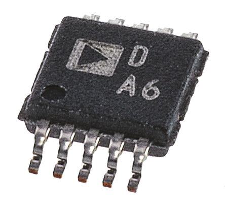
| 产品型号 | AD5667RBRMZ-2 |
| 产品培训模块 | http://www.digikey.cn/PTM/IndividualPTM.page?site=cn&lang=zhs&ptm=19145http://www.digikey.cn/PTM/IndividualPTM.page?site=cn&lang=zhs&ptm=18614http://www.digikey.cn/PTM/IndividualPTM.page?site=cn&lang=zhs&ptm=26125http://www.digikey.cn/PTM/IndividualPTM.page?site=cn&lang=zhs&ptm=26140http://www.digikey.cn/PTM/IndividualPTM.page?site=cn&lang=zhs&ptm=26150http://www.digikey.cn/PTM/IndividualPTM.page?site=cn&lang=zhs&ptm=26147 |
| 产品种类 | 数模转换器- DAC |
| 位数 | 16 |
| 供应商器件封装 | 10-MSOP |
| 其它名称 | AD5667RBRMZ2 |
| 分辨率 | 16 bit |
| 包装 | 管件 |
| 商标 | Analog Devices |
| 安装类型 | 表面贴装 |
| 安装风格 | SMD/SMT |
| 封装 | Tube |
| 封装/外壳 | 10-TFSOP,10-MSOP(0.118",3.00mm 宽) |
| 封装/箱体 | MSOP-10 |
| 工作温度 | -40°C ~ 105°C |
| 工厂包装数量 | 50 |
| 建立时间 | 4µs |
| 接口类型 | Serial |
| 数据接口 | 串行 |
| 最大功率耗散 | 5.75 mW |
| 最大工作温度 | + 105 C |
| 最小工作温度 | - 40 C |
| 标准包装 | 50 |
| 电压参考 | Internal, External |
| 电压源 | 单电源 |
| 电源电压-最大 | 5.5 V |
| 电源电压-最小 | 2.7 V |
| 积分非线性 | +/- 12 LSB |
| 稳定时间 | 4 us |
| 系列 | AD5667R |
| 结构 | Resistor String |
| 转换器数 | 2 |
| 转换器数量 | 2 |
| 输出数和类型 | 2 电压,单极2 电压,双极 |
| 输出类型 | Voltage |
| 采样比 | 250 kSPs |
| 采样率(每秒) | 250k |


- 商务部:美国ITC正式对集成电路等产品启动337调查
- 曝三星4nm工艺存在良率问题 高通将骁龙8 Gen1或转产台积电
- 太阳诱电将投资9.5亿元在常州建新厂生产MLCC 预计2023年完工
- 英特尔发布欧洲新工厂建设计划 深化IDM 2.0 战略
- 台积电先进制程称霸业界 有大客户加持明年业绩稳了
- 达到5530亿美元!SIA预计今年全球半导体销售额将创下新高
- 英特尔拟将自动驾驶子公司Mobileye上市 估值或超500亿美元
- 三星加码芯片和SET,合并消费电子和移动部门,撤换高东真等 CEO
- 三星电子宣布重大人事变动 还合并消费电子和移动部门
- 海关总署:前11个月进口集成电路产品价值2.52万亿元 增长14.8%


PDF Datasheet 数据手册内容提取
Dual, 12-/14-/16-Bit nanoDACs® with 5 ppm/°C On-Chip Reference, I2C® Interface Data Sheet AD5627R/AD5647R/AD5667R, AD5627/AD5667 FEATURES FUNCTIONAL BLOCK DIAGRAMS Low power, smallest pin-compatible, dual nanoDACs VDD GND VREFIN/VREFOUT AD5627R/AD5647R/AD5667R AD5627R/AD5647R/AD5667R 1.25V/2.5V REF 12-/14-/16-bit ADDR BUFFER ADO152n6-2-/c17h6/iA-pbD 1i5t. 62657 V /2.5 V, 5 ppm/°C reference SCL INTERFACELOGIC RREEIINNGGPPIISSUUTTTTEERR RREEGGDDIIAASSCCTTEERR SSDDTTAARRCCIINN BAGG BUFFER VVOOUUTTBA External reference only SDA 3 mm x 3 mm LFCSP and 10-lead MSOP POWER-ON POWER-DOWN RESET LOGIC 2G.u7a Vra tnot 5e.e5d V m poonwoetro snuicp pblyy d esign LDACCLR 06342-001 Power-on reset to zero scale Figure 1. AD5627R/AD5647R/AD5667R Per channel power-down VDD GND VREFIN Hardware LDAC and CLR functions AD5627/AD5667 I2C-compatible serial interface supports standard (100 kHz), APrPofaPcseLts I(sC4 c0Ao0nT ktIrOHozlN ),S a nd high speed (3.4 MHz) modes ADSDCRL INTERFACELOGIC RREEIINNGGPPIISSUUTTTTEERR RREEGGDDIIAASSCCTTEERR SSDDTTAARRCCIINN ABGG BBUUFFFFEERR VVOOUUTTAB SDA Data acquisition systems POWER-ON POWER-DOWN Portable battery-powered instruments RESET LOGIC DPrioggitraal mgamina balned v ooflftsaegte a adnjuds ctumrerennt t sources LDACCLR 06342-002 Figure 2. AD5627/AD5667 Programmable attenuators GENERAL DESCRIPTION The AD5627R/AD5647R/AD5667R, AD5627/AD5667 members The device contains a per-channel power-down feature that of the nanoDAC family are low power, dual, 12-, 14-, 16-bit reduces the current consumption of the device to 480 nA at 5 V buffered voltage-out digital-to-analog converters (DACs) and provides software-selectable output loads while in power- with/without on-chip reference. All devices operate from a single down mode. The low power consumption of this device in 2.7 V to 5.5 V supply, are guaranteed monotonic by design, and normal operation makes it ideally suited to portable battery- have an I2C-compatible serial interface. operated equipment. The on-chip precision output amplifier enables rail-to-rail output swing. The AD5627R/AD5647R/AD5667R have an on-chip reference. The AD5627RBCPZ, AD5647RBCPZ, and AD5667RBCPZ have a The AD5627R/AD5647R/AD5667R, AD5627/AD5667 use a 1.25 V, 5 ppm/°C reference, giving a full-scale output range of 2.5 V; 2-wire I2C-compatible serial interface that operates in standard the AD5627RBRMZ and AD5667RBRMZ have a 2.5 V, 5 ppm/°C (100 kHz), fast (400 kHz), and high speed (3.4 MHz) modes. reference, giving a full-scale output range of 5 V. The on-chip Table 1. Related Devices reference is off at power-up, allowing the use of an external Part No. Description reference. The internal reference is enabled via a software write. AD5663 2.7 V to 5.5 V, dual 16-bit DAC, The AD5667 and AD5627 require an external reference voltage external reference, I2C interface to set the output range of the DAC. AD5623R/AD5643R/AD5663R 2.7 V to 5.5 V, dual 12-, 14-, 16- The AD5627R/AD5647R/AD5667R, AD5627/AD5667 bit DACs, internal reference, incorporate a power-on reset circuit that ensures the DAC I2C interface output powers up to 0 V, and remains there until a valid write AD5625R/AD5645R/AD5665R, 2.7 V to 5.5 V, quad 12-, 14-, 16- AD5625/AD5665 bit DACs, with/without internal takes place. reference, I2C interface Rev. B Document Feedback Information furnished by Analog Devices is believed to be accurate and reliable. However, no responsibility is assumed by Analog Devices for its use, nor for any infringements of patents or other One Technology Way, P.O. Box 9106, Norwood, MA 02062-9106, U.S.A. rights of third parties that may result from its use. Specifications subject to change without notice. No license is granted by implication or otherwise under any patent or patent rights of Analog Devices. Tel: 781.329.4700 ©2007–2016 Analog Devices, Inc. All rights reserved. Trademarks and registered trademarks are the property of their respective owners. Technical Support www.analog.com
AD5627R/AD5647R/AD5667R, AD5627/AD5667 Data Sheet TABLE OF CONTENTS Features .............................................................................................. 1 Write Operation.......................................................................... 21 Applications ....................................................................................... 1 Read Operation........................................................................... 21 Functional Block Diagrams ............................................................. 1 High Speed Mode ....................................................................... 21 General Description ......................................................................... 1 Input Shift Register .................................................................... 23 Revision History ............................................................................... 2 Multiple Byte Operation ............................................................ 23 Specifications ..................................................................................... 3 Broadcast Mode .......................................................................... 23 AC Characteristics ........................................................................ 5 LDAC Function .......................................................................... 23 I2C Timing Specifications ............................................................ 6 Power-Down Modes .................................................................. 25 Absolute Maximum Ratings ............................................................ 8 Power-On Reset and Software Reset........................................ 26 ESD Caution .................................................................................. 8 Clear Pin (CLR) .......................................................................... 26 Pin Configuration and Function Descriptions ............................. 9 Internal Reference Setup (R Versions) .................................... 26 Typical Performance Characteristics ........................................... 10 Application Information ................................................................ 28 Terminology .................................................................................... 18 Using a Reference as a Power Supply for the Theory of Operation ...................................................................... 20 AD5627R/AD5647R/AD5667R, AD5627/AD5667 .................. 28 D/A Section ................................................................................. 20 Bipolar Operation Using the AD5627R/AD5647R/AD5667R, AD5627/AD5667 ......................................................................... 28 Resistor String ............................................................................. 20 Power Supply Bypassing and Grounding ................................ 28 Output Amplifier ........................................................................ 20 Outline Dimensions ....................................................................... 29 Internal Reference ...................................................................... 20 Ordering Guide .......................................................................... 30 External Reference...................................................................... 20 Serial Interface ............................................................................ 21 REVISION HISTORY 9/2016—Rev. A to Rev. B Changed SPI to I2C ........................................................ Throughout 2/2016—Rev. 0 to Rev. A Changes to Internal Reference Section ............................................. 20 Changes to Power-On Reset and Software Reset Section ........... 26 Updated Outline Dimensions .............................................................. 29 Changes to Ordering Guide .................................................................. 30 1/2007—Revision 0: Initial Version Rev. B | Page 2 of 30
Data Sheet AD5627R/AD5647R/AD5667R, AD5627/AD5667 SPECIFICATIONS V = 2.7 V to 5.5 V; R = 2 kΩ to GND; C = 200 pF to GND; V = V ; all specifications T to T , unless otherwise noted. DD L L REFIN DD MIN MAX Table 2. Parameter Min Typ Max Unit Test Conditions/Comments1 STATIC PERFORMANCE2 AD5667R/AD5667 Resolution 16 Bits Relative Accuracy ±8 ±12 LSB Differential Nonlinearity ±1 LSB Guaranteed monotonic by design AD5647R Resolution 14 Bits Relative Accuracy ±2 ±4 LSB Differential Nonlinearity ±0.5 LSB Guaranteed monotonic by design AD5627R/AD5627 Resolution 12 Bits Relative Accuracy ±0.5 ±1 LSB Differential Nonlinearity ±0.25 LSB Guaranteed monotonic by design Zero-Code Error 2 10 mV All 0s loaded to DAC register Offset Error ±1 ±10 mV Full-Scale Error −0.1 ±1 % of FSR All 1s loaded to DAC register Gain Error ±1.5 % of FSR Zero-Code Error Drift ±2 µV/°C Gain Temperature Coefficient ±2.5 ppm Of FSR/°C DC Power Supply Rejection Ratio −100 dB DAC code = midscale ; V = 5 V ± 10% DD DC Crosstalk (External Reference) 15 µV Due to full-scale output change, R = 2 kΩ to GND or 2 kΩ to V L DD 10 µV/mA Due to load current change 8 µV Due to powering down (per channel) DC Crosstalk (Internal Reference) 25 µV Due to full-scale output change, R = 2 kΩ to GND or 2 kΩ to V L DD 20 µV/mA Due to load current change 10 µV Due to powering down (per channel) OUTPUT CHARACTERISTICS3 Output Voltage Range 0 V V DD Capacitive Load Stability 2 nF R = ∞ L 10 nF R = 2 kΩ L DC Output Impedance 0.5 Ω Short-Circuit Current 30 mA V = 5 V DD Power-Up Time 4 µs Coming out of power-down mode; V = 5 V DD REFERENCE INPUTS Reference Current 110 130 µA V = V = 5.5 V REF DD Reference Input Range 0.75 V V DD Reference Input Impedance 50 kΩ REFERENCE OUTPUT (LFCSP_WD PACKAGE) Output Voltage 1.247 1.253 V At ambient Reference TC3 ±10 ppm/°C Output Impedance 7.5 kΩ REFERENCE OUTPUT (MSOP PACKAGE) Output Voltage 2.495 2.505 V At ambient Reference TC3 ±5 ±10 ppm/°C Output Impedance 7.5 kΩ Rev. B | Page 3 of 30
AD5627R/AD5647R/AD5667R, AD5627/AD5667 Data Sheet Parameter Min Typ Max Unit Test Conditions/Comments1 LOGIC INPUTS (ADDR, CLR, LDAC)3 I , Input Current ±1 µA IN V , Input Low Voltage 0.15 × V V INL DD V , Input High Voltage 0.85 × V V INH DD C , Pin Capacitance 2 pF ADDR IN 20 pF CLR, LDAC V , Input Hysteresis 0.1 × V V HYST DD LOGIC INPUTS (SDA, SCL) I , Input Current ±1 µA IN V , Input Low Voltage 0.3 × V V INL DD V , Input High Voltage 0.7 × V V INH DD C , Pin Capacitance 2 pF IN V , Input Hysteresis 0.1 × V V HYST DD LOGIC OUTPUTS (OPEN-DRAIN) V , Output Low Voltage 0.4 V I = 3 mA OL SINK 0.6 V I = 6 mA SINK Floating-State Leakage Current ±1 µA Floating-State Output Capacitance 2 pF POWER REQUIREMENTS V 2.7 5.5 V DD I (Normal Mode)4 V = V , V = GND DD IH DD IL V = 4.5 V to 5.5 V 0.4 0.5 mA Internal reference off DD V = 2.7 V to 3.6 V 0.35 0.45 mA Internal reference off DD V = 4.5 V to 5.5 V 0.95 1.15 mA Internal reference on DD V = 2.7 V to 3.6 V 0.8 0.95 mA Internal reference on DD I (All Power-Down Modes)5 0.48 1 µA V = V , V = GND DD IH DD IL 1 Temperature range: B grade: −40°C to +105°C. 2 Linearity calculated using a reduced code range: AD5667R/AD5667 (Code 512 to Code 65,024); AD5647R (Code 128 to Code 16,256); AD5627R/AD5627 (Code 32 to Code 4064). Output unloaded. 3 Guaranteed by design and characterization, not production tested. 4 Interface inactive. All DACs active. DAC outputs unloaded. 5 All DACs powered down. Rev. B | Page 4 of 30
Data Sheet AD5627R/AD5647R/AD5667R, AD5627/AD5667 AC CHARACTERISTICS V = 2.7 V to 5.5 V; R = 2 kΩ to GND; C = 200 pF to GND; V = V ; all specifications T to T , unless otherwise noted.1 DD L L REFIN DD MIN MAX Table 3. Parameter2 Min Typ Max Unit Test Conditions/Comments3 Output Voltage Settling Time AD5627R/AD5627 3 4.5 µs ¼ to ¾ scale settling to ±0.5 LSB AD5647R 3.5 5 µs ¼ to ¾ scale settling to ±0.5 LSB AD5667R/AD5667 4 7 µs ¼ to ¾ scale settling to ±2 LSB Slew Rate 1.8 V/µs Digital-to-Analog Glitch Impulse 15 nV-s 1 LSB change around major carry transition Digital Feedthrough 0.1 nV-s Reference Feedthrough −90 dB V = 2 V ± 0.1 V p-p, frequency 10 Hz to 20 MHz REF Digital Crosstalk 0.1 nV-s Analog Crosstalk 1 nV-s External reference 4 nV-s Internal reference DAC to DAC Crosstalk 1 nV-s External reference 4 nV-s Internal reference Multiplying Bandwidth 340 kHz V = 2 V ± 0.1 V p-p REF Total Harmonic Distortion −80 dB V = 2 V ± 0.1 V p-p, frequency = 10 kHz REF Output Noise Spectral Density 120 nV/√Hz DAC code = midscale, 1 kHz 100 nV/√Hz DAC code = midscale, 10 kHz Output Noise 15 µV p-p 0.1 Hz to 10 Hz 1 Guaranteed by design and characterization, not production tested. 2 See the Terminology section. 3 Temperature range is −40°C to +105°C, typical at 25°C. Rev. B | Page 5 of 30
AD5627R/AD5647R/AD5667R, AD5627/AD5667 Data Sheet I2C TIMING SPECIFICATIONS V = 2.7 V to 5.5 V; all specifications T to T , f = 3.4 MHz, unless otherwise noted.1 DD MIN MAX SCL Table 4. Parameter Test Conditions/Comments2 Min Max Unit Description f 3 Standard mode 100 kHz Serial clock frequency SCL Fast mode 400 kHz High speed mode, C = 100 pF 3.4 MHz B High speed mode, C = 400 pF 1.7 MHz B t Standard mode 4 μs t , SCL high time 1 HIGH Fast mode 0.6 μs High speed mode, C = 100 pF 60 ns B High speed mode, C = 400 pF 120 ns B t Standard mode 4.7 μs t , SCL low time 2 LOW Fast mode 1.3 μs High speed mode, C = 100 pF 160 ns B High speed mode, C = 400 pF 320 ns B t Standard mode 250 ns t , data setup time 3 SU;DAT Fast mode 100 ns High speed mode 10 ns t Standard mode 0 3.45 μs t , data hold time 4 HD;DAT Fast mode 0 0.9 μs High speed mode, C = 100 pF 0 70 ns B High speed mode, C = 400 pF 0 150 ns B t Standard mode 4.7 μs t setup time for a repeated start condition 5 SU;STA, Fast mode 0.6 μs High speed mode 160 ns t Standard mode 4 μs t , hold time (repeated) start condition 6 HD;STA Fast mode 0.6 μs High speed mode 160 ns t Standard mode 4.7 μs t , bus free time between a stop and a start condition 7 BUF Fast mode 1.3 μs t Standard mode 4 μs t , setup time for a stop condition 8 SU;STO Fast mode 0.6 μs High speed mode 160 ns t Standard mode 1000 ns t , rise time of SDA signal 9 RDA Fast mode 300 ns High speed mode, C = 100 pF 10 80 ns B High speed mode, C = 400 pF 20 160 ns B t Standard mode 300 ns t , fall time of SDA signal 10 FDA Fast mode 300 ns High speed mode, C = 100 pF 10 80 ns B High speed mode, C = 400 pF 20 160 ns B t Standard mode 1000 ns t , rise time of SCL signal 11 RCL Fast mode 300 ns High speed mode, C = 100 pF 10 40 ns B High speed mode, C = 400 pF 20 80 ns B t Standard mode 1000 ns t , rise time of SCL signal after a repeated start condition and after 11A RCL1 an acknowledge bit Fast mode 300 ns High speed mode, C = 100 pF 10 80 ns B High speed mode, C = 400 pF 20 160 ns B Rev. B | Page 6 of 30
Data Sheet AD5627R/AD5647R/AD5667R, AD5627/AD5667 Parameter Test Conditions/Comments2 Min Max Unit Description t Standard mode 300 ns t , fall time of SCL signal 12 FCL Fast mode 300 ns High speed mode, C = 100 pF 10 40 ns B High speed mode, C = 400 pF 20 80 ns B t13 Standard mode 10 ns LDAC pulse width low Fast mode 10 ns High speed mode 10 ns t14 Standard mode 300 ns Falling edge of 9th SCL clock pulse of last byte of valid write to LDAC falling edge Fast mode 300 ns High speed mode 30 ns t15 Standard mode 20 ns CLR pulse width low Fast mode 20 ns High speed mode 20 ns t 4 Fast mode 0 50 ns Pulse width of spike suppressed SP High speed mode 0 10 ns 1 See Figure 3. High speed mode timing specification applies only to the AD5627RBRMZ-2/AD5627BRMZ-2REEL7 and AD5667RBRMZ-2/AD5667BRMZ-2REEL7. 2 CB refers to the capacitance on the bus line. 3 The SDA and SCL timing is measured with the input filters enabled. Switching off the input filters improves the transfer rate but has a negative effect on EMC behavior of the device. 4 Input filtering on the SCL and SDA inputs suppresses noise spikes that are less than 50 ns for fast mode or 10 ns for high speed mode. t11 t12 t6 t2 SCL t6 t1 t5 t8 t4 t3 t10 t9 SDA t7 P S S t14 P LDAC* t13 CLR *ASYNCHRONOUS LDAC UPDATE MODE. t15 06342-003 Figure 3. 2-Wire Serial Interface Timing Diagram Rev. B | Page 7 of 30
AD5627R/AD5647R/AD5667R, AD5627/AD5667 Data Sheet ABSOLUTE MAXIMUM RATINGS T = 25°C, unless otherwise noted. Stresses at or above those listed under Absolute Maximum A Ratings may cause permanent damage to the product. This is a Table 5. stress rating only; functional operation of the product at these Parameter Rating or any other conditions above those indicated in the operational V to GND −0.3 V to +7 V DD section of this specification is not implied. Operation beyond V to GND −0.3 V to V + 0.3 V OUT DD the maximum operating conditions for extended periods may V /V to GND −0.3 V to V + 0.3 V REFIN REFOUT DD affect product reliability. Digital Input Voltage to GND −0.3 V to V + 0.3 V DD Operating Temperature Range, Industrial −40°C to +105°C ESD CAUTION Storage Temperature Range −65°C to +150°C Junction Temperature (T maximum) 150°C J Power Dissipation (T max − T )/θ J A JA θ Thermal Impedance JA LFCSP_WD Package (4-Layer Board) 61°C/W MSOP Package 150.4°C/W Reflow Soldering Peak Temperature, Pb-Free 260°C ± 5°C Rev. B | Page 8 of 30
Data Sheet AD5627R/AD5647R/AD5667R, AD5627/AD5667 PIN CONFIGURATION AND FUNCTION DESCRIPTIONS VOUTA 1 10 VREFIN VOUTA 1 10 VREFIN/VREFOUT AD5627/ AD5627R/ VOUTB 2 AD5667 9 VDD VOUTB 2 AD5647R/ 9 VDD GND 3 8 SDA GND 3 AD5667R 8 SDA LDAC 4 TOP VIEW 7 SCL LDAC 4 TOP VIEW 7 SCL (Not to Scale) (Not to Scale) CLR 5 6 ADDR CLR 5 6 ADDR EXPOONS LEFDC PSAPD P TAICEDK ATGOE G.ND 06342-101 EXPOONS LEFDC PSAPD P TAICEDK ATGOE G.ND 06342-102 Figure 4. AD5627/AD5667 Pin Configuration Figure 5. AD5627R/AD5647R/AD5667R Pin Configuration Table 6. Pin Function Descriptions Pin No. Mnemonic Description 1 V A Analog Output Voltage from DAC A. The output amplifier has rail-to-rail operation. OUT 2 V B Analog Output Voltage from DAC B. The output amplifier has rail-to-rail operation. OUT 3 GND Ground reference point for all circuitry on the device. 4 LDAC Pulsing this pin low allows any or all DAC registers to be updated if the inputs have new data. This allows simultaneous updates of all DAC outputs. Alternatively, this pin can be tied permanently low. 5 CLR Asynchronous Clear Input. The CLR input is falling-edge sensitive. While CLR is low, all LDAC pulses are ignored. When CLR is activated, zero scale is loaded to all input and DAC registers. This clears the output to 0 V. The device exits clear code mode on the falling edge of the 9th clock pulse of the last byte of valid write. If CLR is activated during a write sequence, the write is aborted. If CLR is activated during high speed mode the device will exit high speed mode. 6 ADDR Three-State Address Input. Sets the two least significant bits (Bit A1, Bit A0) of the 7-bit slave address. 7 SCL Serial Clock Line. This is used in conjunction with the SDA line to clock data into or out of the 24-bit input register. 8 SDA Serial Data Line. This is used in conjunction with the SCL line to clock data into or out of the 24-bit input register. It is a bidirectional, open-drain data line that should be pulled to the supply with an external pull-up resistor. 9 V Power Supply Input. These devices can be operated from 2.7 V to 5.5 V, and the supply should be decoupled with a DD 10 μF capacitor in parallel with a 0.1 μF capacitor to GND. 10 V /V The AD5627R/AD5647R/AD5667R have a common pin for reference input and reference output. When using the REFIN REFOUT internal reference, this is the reference output pin. When using an external reference, this is the reference input pin. The default for this pin is as a reference input. (The internal reference and reference output are only available on R suffix versions.) The AD5627/AD5667 have a reference input pin only. Rev. B | Page 9 of 30
AD5627R/AD5647R/AD5667R, AD5627/AD5667 Data Sheet TYPICAL PERFORMANCE CHARACTERISTICS 10 1.0 VDD = VREF = 5V VDD = VREF = 5V 8 TA = 25°C 0.8 TA = 25°C 6 0.6 4 0.4 INL ERROR (LSB) ––2402 DNL ERROR (LSB) ––000...4220 –6 –0.6 –8 –0.8 –100 5k 10k 15k 20k 25k 30CkOD3E5k 40k 45k 50k 55k 60k 65k 06342-005 –1.00 10k 20k 30CkODE 40k 50k 60k 06342-007 Figure 6. AD5667 INL, External Reference Figure 9. AD5667 DNL, External Reference 4 0.5 VDD = VREF = 5V VDD = VREF = 5V 3 TA = 25°C 0.4 TA = 25°C 0.3 2 0.2 INL ERROR (LSB) –101 DNL ERROR (LSB) ––000...2110 –2 –0.3 –3 –0.4 –40 2500 5000 75C0O0DE 10000 12500 15000 06342-006 –0.50 2500 5000 75C0O0DE 10000 12500 15000 06342-008 Figure 7. AD5647R INL, External Reference Figure 10. DNL AD5647R, External Reference 1.0 0.20 VDD = VREF = 5V VDD = VREF = 5V 0.8 TA = 25°C 0.15 TA = 25°C 0.6 0.10 0.4 INL ERROR (LSB) ––000...4220 DNL ERROR (LSB) –00..00550 –0.10 –0.6 –0.15 –0.8 –1.00 500 1000 1500 2C0O0D0E 2500 3000 3500 4000 06342-100 –0.200 500 1000 1500 2C0O00DE 2500 3000 3500 4000 06342-009 Figure 8. AD5627 INL, External Reference Figure 11. AD5627 DNL, External Reference Rev. B | Page 10 of 30
Data Sheet AD5627R/AD5647R/AD5667R, AD5627/AD5667 10 1.0 VDD = 5V VDD=5V 8 VREFOUT = 2.5V 0.8 VREFOUT=2.5V TA = 25°C TA=25°C 6 0.6 B) 4 SB) 0.4 R (LS 2 OR (L 0.2 RO 0 RR 0 R E L E –2 NL –0.2 N D I –0.4 –4 –0.6 –6 –0.8 –8 –1.0 –10 0 0 0 0 0 0 0 0 0 0 0 0 0 0 0 5000 10000 15000 20000 25000 30000CODE35000 40000 45000 50000 55000 60000 65000 06342-010 500 1000 1500 2000 2500 3000CODE3500 4000 4500 5000 5500 6000 6500 06342-013 Figure 12. AD5667R INL, 2.5 V Internal Reference Figure 15. AD5667R DNL, 2.5 V Internal Reference 4 0.5 VDD=5V VDD = 5V 3 VREFOUT=2.5V 0.4 VREFOUT = 2.5V TA=25°C TA = 25°C 0.3 2 0.2 B) B) S 1 S R (L R (L 0.1 RO 0 RO 0 R R E E NL –1 NL –0.1 I D –0.2 –2 –0.3 –3 –0.4 –4 –0.5 0 1250 2500 3750 5000 6250 7500CODE8750 10000 11250 12500 13750 15000 16250 06342-011 0 1250 2500 3750 5000 6250 7500CODE8750 10000 11250 12500 13750 15000 16250 06342-014 Figure 13. AD5647R INL, 2.5 V Internal Reference Figure 16. AD5647R DNL, 2.5 V Internal Reference 1.0 0.20 VDD=5V VDD = 5V 0.8 VREFOUT=2.5V 0.15 VREFOUT = 2.5V TA=25°C TA = 25°C 0.6 0.10 0.4 INL ERROR (LSB) –00..220 DNL ERROR (LSB)–00..00550 –0.4 –0.10 –0.6 –0.15 –0.8 –1.00 500 1000 1500 2C0O0D0E 2500 3000 3500 4000 06342-012 –0.200 500 1000 1500 2C0O0D0E 2500 3000 3500 4000 06342-015 Figure 14. AD5627R INL, 2.5 V Internal Reference Figure 17. AD5627R DNL, 2.5 V Internal Reference Rev. B | Page 11 of 30
AD5627R/AD5647R/AD5667R, AD5627/AD5667 Data Sheet 10 1.0 VDD = 3V VDD = 3V 8 VREFOUT = 1.25V 0.8 VREFOUT = 1.25V TA = 25°C TA = 25°C 6 0.6 4 0.4 B) B) R (LS 2 R (LS 0.2 RO 0 RO 0 R R NL E –2 NL E –0.2 I –4 D –0.4 –6 –0.6 –8 –0.8 –10 –1.0 0 0 0 0 0 0 0 0 0 0 0 0 0 0 0 0 0 0 0 0 0 0 0 0 0 0 0 0 0 0 0 0 0 0 0 0 0 0 0 0 0 0 0 0 0 0 0 0 0 0 0 0 0 0 50 100 150 200 250 300COD350E 400 450 500 550 600 650 06342-016 50 100 150 200 250 300COD350E 400 450 500 550 600 650 06342-019 Figure 18. AD5667R INL,1.25 V Internal Reference Figure 21. AD5667R DNL,1.25 V Internal Reference 4 0.5 VDD = 3V VDD = 3V 3 VREFOUT = 1.25V 0.4 VREFOUT = 1.25V TA = 25°C TA = 25°C 0.3 2 0.2 B) B) R (LS 1 R (LS 0.1 RRO 0 RRO 0 NL E –1 NL E –0.1 I D –0.2 –2 –0.3 –3 –0.4 –4 –0.5 0 0 0 0 0 0 0 0 0 0 0 0 0 0 0 0 0 0 0 0 0 0 0 0 0 0 0 0 5 0 5 0 5 0 5 0 5 0 5 0 5 5 0 5 0 5 0 5 0 5 0 5 0 5 12 25 37 50 62 75COD87E 100 112 125 137 150 162 06342-017 12 25 37 50 62 75COD87E 100 112 125 137 150 162 06342-020 Figure 19. AD5647R INL, 1.25 V Internal Reference Figure 22. AD5647R DNL,1.25 V Internal Reference 1.0 0.20 VDD = 3V VDD = 3V 0.8 VREFOUT = 1.25V 0.15 VREFOUT = 1.25V TA = 25°C TA = 25°C 0.6 0.10 0.4 B) B) R (LS 0.2 R (LS 0.05 RO 0 RO 0 R R NL E –0.2 NL E –0.05 I –0.4 D –0.10 –0.6 –0.15 –0.8 –1.00 500 1000 1500 2C0O0D0E 2500 3000 3500 4000 06342-018 –0.200 500 1000 1500 2C0O0D0E 2500 3000 3500 4000 06342-021 Figure 20. AD5627R INL,1.25 V Internal Reference Figure 23. AD5627R DNL, 1.25 V Internal Reference Rev. B | Page 12 of 30
Data Sheet AD5627R/AD5647R/AD5667R, AD5627/AD5667 8 0 VDD = 5V –0.02 6 MAX INL VDD = VREF = 5V –0.04 4 GAIN ERROR –0.06 B) 2 SR) –0.08 OR (LS 0 MAX DNL R (% F –0.10 ERR –2 MIN DNL RRO –0.12 E –0.14 FULL-SCALE ERROR –4 MIN INL –0.16 –6 –0.18 –8–40 –20 0 TEM2P0ERATU4R0E (°C)60 80 100 06342-022 –0.20–40 –20 0 TEM2P0ERATU4R0E (°C)60 80 100 06342-025 Figure 24. INL Error and DNL Error vs. Temperature Figure 27. Gain Error and Full-Scale Error vs. Temperature 10 1.5 8 MAX INL 1.0 ZERO-SCALE ERROR 6 VDD = 5V 0.5 4 TA = 25°C R (LSB) 20 MAX DNL R (mV) –0.50 O O ERR –2 MIN DNL ERR –1.0 –4 –1.5 –6 OFFSET ERROR MIN INL –2.0 –8 –100.75 1.25 1.75 2.25 V2.R7E5F (V3).25 3.75 4.25 4.75 06342-023 –2.5–40 –20 0 TEM2P0ERATU4R0E (°C)60 80 100 06342-026 Figure 25. INL and DNL Error vs. VREF Figure 28. Zero-Scale Error and Offset Error vs. Temperature 8 1.0 6 MAX INL TA = 25°C 0.5 4 GAIN ERROR B) 2 SR) 0 OR (LS 0 MAX DNL R (% F –0.5 FULL-SCALE ERROR RR MIN DNL RO E –2 R E –1.0 –4 MIN INL –1.5 –6 –82.7 3.2 3.7 VDD 4(V.2) 4.7 5.2 06342-024 –2.02.7 3.2 3.7 VDD 4(V.2) 4.7 5.2 06342-027 Figure 26. INL and DNL Error vs. Supply Figure 29. Gain Error and Full-Scale Error vs. Supply Rev. B | Page 13 of 30
AD5627R/AD5647R/AD5667R, AD5627/AD5667 Data Sheet 1.0 0.5 TA = 25°C DAC LOADED WITH DAC LOADED WITH 0.4 FULL-SCALE ZERO-SCALE 0.5 ZERO-SCALE ERROR SOURCING CURRENT SINKING CURRENT 0.3 0 V) 0.2 OR (mV) –0.5 OLTAGE ( 0.10 VVDREDF=O U3VT = 1.25V RR –1.0 R V E O –0.1 R R –1.5 E –0.2 –0.3 VDD= 5V –2.0 OFFSET ERROR VREFOUT = 2.5V –0.4 –2.52.7 3.2 3.7 VDD 4(V.2) 4.7 5.2 06342-028 –0.5–10 –8 –6 –4 C–2URRE0NT (mA2) 4 6 8 10 06342-031 Figure 30. Zero-Scale Error and Offset Error vs. Supply Figure 33. Headroom at Rails vs. Source and Sink 18 6 VDD= 3.6V VDD= 5V FULL SCALE 16 VDD= 5.5V 5 VTAR E=F O25U°TC = 2.5V 14 S 4 3/4 SCALE CE 12 VI R OF DE 108 (V)OUT 3 MIDSCALE E V 2 B M 1/4 SCALE U 6 N 1 4 2 0 ZERO SCALE 00.30 0.32 0.34 0.36IDD (0m.3A8) 0.40 0.42 0.44 06342-029 –1–30 –20 –10 CURRE0NT (mA) 10 20 30 06342-046 Figure 31. IDD Histogram with External Reference Figure 34. AD5627R/AD5647R/AD5667R with 2.5 V Reference, Source and Sink Capability 14 12 VREFOUT = 1.25V VVDDDD== 35..65VV 4 VVDREDF=O U3VT = 1.25V TA = 25°C 3 S 10 FULL SCALE E C VI MBER OF DE 86 VREFOUT = 2.5V V (V)OUT 12 M3/I4D SSCCAALLEE U 1/4 SCALE N 4 2 0 ZERO SCALE 0 0.740.750.760.770.780.790.800.810.820.830.840.850.860.87ID0.88D 0.89(m0.90A0.91)0.920.930.940.950.960.970.980.991.001.011.021.031.04 06342-030 –1–30 –20 –10 CURRE0NT (mA) 10 20 30 06342-047 Figure 32. IDD Histogram with Internal Reference Figure 35. AD5627R/AD5647R/AD5667R with 1.25 V Reference, Source and Sink Capability Rev. B | Page 14 of 30
Data Sheet AD5627R/AD5647R/AD5667R, AD5627/AD5667 0.9 TA = 25°C 0.8 VDD = 5V, VREFOUT = 2.5V 0.7 0.6 VDD = VREF = 5V TA = 25°C FULL-SCALE CODE CHANGE A) 0.5 0x0000TO 0xFFFF (mDD 0.4 VDD = VREF = 5V OANUDT P2U00Tp LFOTAOD EGDN DWITH 2kΩ I 0.3 VOUT= 909mV/DIV 0.2 1 0.1 0512 10512 20512 305C1O2DE 40512 50512 60512 06342-060 TIME BASE = 4µs/DIV 06342-048 Figure 36. Supply Current vs. Code Figure 39. Full-Scale Settling Time, 5 V 0.40 VDD = VREF = 5V 0.35 TA = 25°C 0.30 0.25 A) m (DD 0.20 VDD I 1 0.15 0.10 MAX(C2) 420.0mV 2 0.05 VOUT 02.7TA = 25°C3.2 S3U.7PPLY VO4L.T2AGE (V)4.7 5.2 06342-061 CH1 2.0V CH2 500mV AM 1C0H01µ s 1 215.M28SV/s 8.0ns/pt 06342-049 Figure 37. Supply Current vs. Supply Voltage Figure 40. Power-On Reset to 0 V 0.45 SYNC 0.40 VDD = VREFIN = 5V 1 0.35 SLCK 3 0.30 VDD = VREFIN = 3V A) 0.25 m (DD 0.20 I 0.15 VOUT 0.10 VDD = 5V 2 0.05 0–40 –20 0 TEM2P0ERATU4R0E (°C)60 80 100 06342-063 CCHH13 55..00VV CH2 500mV M400ns A CH1 1.4V 06342-050 Figure 38. Supply Current vs. Temperature Figure 41. Exiting Power-Down to Midscale Rev. B | Page 15 of 30
AD5627R/AD5647R/AD5667R, AD5627/AD5667 Data Sheet 2.538 2.537 VDD= VREF = 5V VDD = VREF = 5V 2.536 T5nAs =/S 2A5M°CPLE NUMBER DTAA C= 2L5O°ACDED WITH MIDSCALE 2.535 GLITCH IMPULSE = 9.494nV 2.534 1LSB CHANGE AROUND 2.533 MIDSCALE (0x8000 TO 0x7FFF) 2.532 (V)OUT222...555233901 2µV/DIV1 V 2.528 2.527 2.526 2.525 2.524 2.523 22..5522120 50 100 150 S2A00MPL2E5 0NUM30B0ER350 400 450 512 06342-058 4s/DIV 06342-051 Figure 42. Digital-to-Analog Glitch Impulse (Negative) Figure 45. 0.1 Hz to 10 Hz Output Noise Plot, External Reference 2.498 VDD= VREF = 5V VDD = 5V TA = 25°C VREFOUT = 2.5V 2.497 5ns/SAMPLE NUMBER TA = 25°C ANALOG CROSSTALK = 0.424nV DAC LOADED WITH MIDSCALE 2.496 V) 2.495 DIV (UT µV/1 VO2.494 10 2.493 2.492 2.4910 50 100 150 S2A0M0PLE25 N0UM3B0E0R 350 400 450 512 06342-059 5s/DIV 06342-052 Figure 43. Analog Crosstalk, External Reference Figure 46. 0.1 Hz to 10 Hz Output Noise Plot, 2.5 V Internal Reference 2.496 2.494 VDD = 3V 2.492 VREFOUT = 1.25V 2.490 TA = 25°C DAC LOADED WITH MIDSCALE 2.488 2.486 2.484 2.482 2.480 V (V)OUT222...444777468 5µV/DIV1 2.472 2.470 2.468 2.466 VDD= 5V 2.464 VREFOUT = 2.5V 2.462 TA = 25°C 2.460 5ns/SAMPLE NUMBER 22..4455680 50 100 150 S2A00MPLA2E5N 0NAULMO30GB0E CRR3O5S0STA40L0K = 445.4062nV512 06342-062 4s/DIV 06342-053 Figure 44. Analog Crosstalk, Internal Reference Figure 47. 0.1 Hz to 10 Hz Output Noise Plot,1.25 V Internal Reference Rev. B | Page 16 of 30
Data Sheet AD5627R/AD5647R/AD5667R, AD5627/AD5667 800 16 TA = 25°C VREF = VDD 700 MIDSCALE LOADED TA = 25°C 14 Hz) 600 VDD=3V √ 12 V/ 500 n OISE ( 400 E (µs) 10 N M T TI UTPU 300 VDD= 5V 8 VDD=5V O 200 VREFOUT = 2.5V 6 100 VDD= 3V VREFOUT = 1.25V 0100 1k FREQU1E0NkCY (Hz) 100k 1M 06342-054 40 1 2 3 CA4PACITA5NCE 6(nF) 7 8 9 10 06342-056 Figure 48. Noise Spectral Density, Internal Reference Figure 50. Settling Time vs. Capacitive Load –20 5 VDD = 5V VDD = 5V –30 TDAA C= 2L5O°ACDED WITH FULL SCALE 0 TA = 25°C VREF = 2V ± 0.3V p-p –5 –40 –10 –50 –15 dB) –60 dB) ( ( –20 –70 –25 –80 –30 –90 –35 –100 2k F4RkEQUENCY 6(Hkz) 8k 10k 06342-055 –4010k 100kFREQUENCY (Hz)1M 10M 06342-057 Figure 49. Total Harmonic Distortion Figure 51. Multiplying Bandwidth Rev. B | Page 17 of 30
AD5627R/AD5647R/AD5667R, AD5627/AD5667 Data Sheet TERMINOLOGY Relative Accuracy or Integral Nonlinearity (INL) Output Voltage Settling Time For the DAC, relative accuracy or integral nonlinearity is a Output voltage settling time is the amount of time it takes for measurement of the maximum deviation, in LSBs, from a straight the output of a DAC to settle to a specified level for a ¼ to ¾ line passing through the endpoints of the DAC transfer function. full-scale input change and is measured from the rising edge of the stop condition. Differential Nonlinearity (DNL) Differential nonlinearity is the difference between the measured Digital-to-Analog Glitch Impulse change and the ideal 1 LSB change between any two adjacent codes. Digital-to-analog glitch impulse is the impulse injected into the A specified differential nonlinearity of ±1 LSB maximum ensures analog output when the input code in the DAC register changes monotonicity. This DAC is guaranteed monotonic by design. state. It is normally specified as the area of the glitch in nV-s, and is measured when the digital input code is changed by 1 LSB at Zero-Code Error the major carry transition (0x7FFF to 0x8000) (see Figure 42). Zero-code error is a measurement of the output error when zero scale (0x0000) is loaded to the DAC register. Ideally, the Digital Feedthrough output should be 0 V. The zero-code error is always positive in Digital feedthrough is a measure of the impulse injected into the AD5667R because the output of the DAC cannot go below the analog output of the DAC from the digital inputs of the 0 V due to a combination of the offset errors in the DAC and DAC, but is measured when the DAC output is not updated. It the output amplifier. Zero-code error is expressed in mV. is specified in nV-s, and measured with a full-scale code change on the data bus, that is, from all 0s to all 1s and vice versa. Full-Scale Error Full-scale error is a measurement of the output error when full- Reference Feedthrough scale code (0xFFFF) is loaded to the DAC register. Ideally, the Reference feedthrough is the ratio of the amplitude of the signal output should be V − 1 LSB. Full-scale error is expressed in % at the DAC output to the reference input when the DAC output DD of full-scale range (FSR). is not being updated. It is expressed in dB. Gain Error Output Noise Spectral Density Gain error is a measure of the span error of the DAC. It is the Output noise spectral density is a measurement of the internally deviation in slope of the DAC transfer characteristic from ideal generated random noise. Random noise is characterized as a expressed in % of FSR. spectral density. It is measured by loading the DAC to midscale and measuring noise at the output. It is measured in nV/√Hz. A Zero-Code Error Drift plot of noise spectral density can be seen in Figure 48. Zero-code error drift is a measurement of the change in zero- code error with a change in temperature. It is expressed in µV/°C. DC Crosstalk DC crosstalk is the dc change in the output level of one DAC in Gain Temperature Coefficient response to a change in the output of another DAC. It is measured Gain temperature coefficient is a measurement of the change in with a full-scale output change on one DAC (or soft power-down gain error with changes in temperature. It is expressed in ppm and power-up) while monitoring another DAC kept at midscale. of FSR/°C. It is expressed in μV. Offset Error DC crosstalk due to load current change is a measure of the Offset error is a measure of the difference between V (actual) OUT impact that a change in load current on one DAC has to and V (ideal) expressed in mV in the linear region of the OUT another DAC kept at midscale. It is expressed in µV/mA. transfer function. Offset error is measured on the AD5667R with code 512 loaded in the DAC register. It can be negative or Digital Crosstalk positive. Digital crosstalk is the glitch impulse transferred to the output of one DAC at midscale in response to a full-scale code change DC Power Supply Rejection Ratio (PSRR) (all 0s to all 1s and vice versa) in the input register of another DC PSRR indicates how the output of the DAC is affected by DAC. It is measured in standalone mode and is expressed in nV-s. changes in the supply voltage. PSRR is the ratio of the change in V to a change in V for full-scale output of the DAC. It is OUT DD measured in dB. V is held at 2 V and V is varied by ±10%. REF DD Rev. B | Page 18 of 30
Data Sheet AD5627R/AD5647R/AD5667R, AD5627/AD5667 Analog Crosstalk Multiplying Bandwidth Analog crosstalk is the glitch impulse transferred to the output The multiplying bandwidth is a measure of the finite bandwidth of one DAC due to a change in the output of another DAC. It is of the amplifiers within the DAC. A sine wave on the reference measured by loading one of the input registers with a full-scale (with full-scale code loaded to the DAC) appears on the output. code change (all 0s to all 1s and vice versa), then executing a The multiplying bandwidth is the frequency at which the output software LDAC and monitoring the output of the DAC whose amplitude falls to 3 dB below the input. digital code was not changed. The area of the glitch is expressed Total Harmonic Distortion (THD) in nV-s. THD is the difference between an ideal sine wave and the DAC-to-DAC Crosstalk attenuated version using the DAC. The sine wave is used as the DAC-to-DAC crosstalk is the glitch impulse transferred to the reference for the DAC, and the THD is a measurement of the output of one DAC due to a digital code change and subsequent harmonics present on the DAC output. It is measured in dB. analog output change of another DAC. It is measured by loading the attack channel with a full-scale code change (all 0s to all 1s and vice versa) with LDAC low while monitoring the output of the victim channel that is at midscale. The energy of the glitch is expressed in nV-s. Rev. B | Page 19 of 30
AD5627R/AD5647R/AD5667R, AD5627/AD5667 Data Sheet THEORY OF OPERATION D/A SECTION R The AD5627R/AD5647R/AD5667R, AD5627/AD5667 DACs are fabricated on a CMOS process. The architecture consists of a R string DAC followed by an output buffer amplifier. Figure 52 shows a block diagram of the DAC architecture. R TO OUTPUT VDD OUTPUT AMPLIFIER AMPLIFIER GAIN = +2 REF (+) REGDIASCTER RSETSRISINTOGR VOUT REF (–) R GND 06342-032 R Because the input coFdiignugre t 5o2 .t hDeA CD AArcChi tiesc stutrrae ight binary, the ideal 06342-033 Figure 53. Resistor String output voltage when using an external reference is given by INTERNAL REFERENCE D V =V × OUT REFIN 2N The AD5627R/AD5647R/AD5667R feature an on-chip reference. Versions without the R suffix require an external reference. The The ideal output voltage when using the internal reference is on-chip reference is off at power-up and enabled via a write to a given by control register. See the Internal Reference Setup section for details. V =2×V × D Versions packaged in a 10-lead LFCSP package have a 1.25 V OUT REFOUT 2N reference, giving a full-scale output of 2.5 V. These devices can operate with a V supply of 2.7 V to 5.5 V. Versions packaged where: DD in a 10-lead MSOP package have a 2.5 V reference, giving a full- D is the decimal equivalent of the binary code that is loaded to scale output of 5 V. The devices are functional with a V supply DD the DAC register: of 4.5 V to 5.5 V, but with a V supply of less than 5 V, the output DD 0 to 4095 for AD5627R/AD5627 (12-bit). is clamped to VDD. See the Ordering Guide for a full list of 0 to 16,383 for AD5647R (14-bit). models. The internal reference associated with each device is 0 to 65,535 for AD5667R/AD5667 (16-bit). available at the VREFOUT pin. N is the DAC resolution. A buffer is required if the reference output drives external loads. When using the internal reference, it is recommended that a RESISTOR STRING 100 nF capacitor be placed between the reference output and The resistor string is shown in Figure 53. It is simply a string of GND for reference stability. resistors, each of value R. The code loaded to the DAC register EXTERNAL REFERENCE determines at which node on the string the voltage is tapped off to be fed into the output amplifier. The voltage is tapped off by The AD5627/AD5667 require an external reference, which is closing one of the switches connecting the string to the amplifier. applied at the VREFIN pin. The VREFIN pin on the AD5627R/ Because it is a string of resistors, it is guaranteed monotonic. AD5647R/AD5667R allows the use of an external reference if OUTPUT AMPLIFIER the application requires it. The default condition of the on-chip reference is off at power-up. All devices can be operated from a The output buffer amplifier can generate rail-to-rail voltages on single 2.7 V to 5.5 V supply. the output, which gives an output range of 0 V to V . It can drive a DD load of 2 kΩ in parallel with 1000 pF to GND. The source and sink capabilities of the output amplifier can be seen in Figure 33 and Figure 34. The slew rate is 1.8 V/µs with a ¼ to ¾ full-scale settling time of 7 µs. Rev. B | Page 20 of 30
Data Sheet AD5627R/AD5647R/AD5667R, AD5627/AD5667 SERIAL INTERFACE WRITE OPERATION The AD5627R/AD5647R/AD5667R, AD5627/AD5667 have 2- When writing to the AD5627R/AD5647R/AD5667R, wire I2C-compatible serial interfaces (refer to I2C-Bus AD5627/AD5667, the user must begin with a start command Specification, Version 2.1, January 2000, available from Philips followed by an address byte (R/W= 0), after which the DAC Semiconductor). The AD5627R/AD5647R/AD5667R, acknowledges that it is prepared to receive data by pulling SDA AD5627/AD5667 can be connected to an I2C bus as a slave low. The AD5627R/AD5647R/AD5667R, AD5627/AD5667 device, under the control of a master device. See Figure 3 for a requires two bytes of data for the DAC and a command byte timing diagram of a typical write sequence. that controls various DAC functions. Three bytes of data must therefore be written to the DAC, the command byte followed by The AD5627R/AD5647R/AD5667R, AD5627/AD5667 support the most significant data byte and the least significant data byte, standard (100 kHz), fast (400 kHz), and high speed (3.4 MHz) as shown in Figure 54. All these data bytes are acknowledged by data transfer modes. High speed operation is only available on the AD5627R/AD5647R/AD5667R, AD5627/AD5667. A stop select models. See the Ordering Guide for a full list of models. condition follows. Support is not provided for 10-bit addressing and general call addressing. READ OPERATION The AD5627R/AD5647R/AD5667R, AD5627/AD5667 each have When reading data back from the AD5627R/AD5647R/AD5667R, a 7-bit slave address. The five MSBs are 00011 and the two LSBs AD5627/AD5667, the user begins with a start command (A1, A0) are set by the state of the ADDR address pin. The followed by an address byte (R/W = 1), after which the DAC facility to make hardwired changes to ADDR allows the user to acknowledges that it is prepared to transmit data by pulling incorporate up to three of these devices on one bus, as outlined SDA low. Three bytes of data are then read from the DAC, in Table 7. which are acknowledged by the master, as shown in Figure 55. A stop condition follows. Table 7. Device Address Selection ADDR Pin Connection A1 A0 HIGH SPEED MODE VDD 0 0 The AD5627RBRMZ and the AD5667RBRMZ offer high speed No Connection 1 0 serial communication with a clock frequency of 3.4 MHz. See GND 1 1 the Ordering Guide for details. High speed mode communication commences after the master The 2-wire serial bus protocol operates as follows: addresses all devices connected to the bus with the Master Code 1. The master initiates data transfer by establishing a start 00001XXX to indicate that a high speed mode transfer is to begin condition when a high-to-low transition on the SDA line (see Figure 56). No device connected to the bus is permitted to occurs while SCL is high. The following byte is the address acknowledge the high speed master code. Therefore, the code is byte, which consists of the 7-bit slave address. The slave followed by a no acknowledge. The master must then issue a address corresponding to the transmitted address responds repeated start followed by the device address. The selected by pulling SDA low during the 9th clock pulse (this is termed device then acknowledges the address. the acknowledge bit). At this stage, all other devices on the All devices continue to operate in high speed mode until the bus remain idle while the selected device waits for data to master issues a stop condition. When the stop condition is be written to, or read from, the shift register. issued, the devices return to standard/fast mode. The device 2. Data is transmitted over the serial bus in sequences of nine also returns to standard/fast mode when CLR is activated while clock pulses (eight data bits followed by an acknowledge the device is in high speed mode. bit). The transitions on the SDA line must occur during the low period of SCL and remain stable during the high period of SCL. 3. When all data bits have been read or written, a stop condition is established. In write mode, the master pulls the SDA line high during the 10th clock pulse to establish a stop condition. In read mode, the master issues a no acknowledge for the 9th clock pulse (that is, the SDA line remains high). The master then brings the SDA line low before the 10th clock pulse, and then high during the 10th clock pulse to establish a stop condition. Rev. B | Page 21 of 30
AD5627R/AD5647R/AD5667R, AD5627/AD5667 Data Sheet 1 9 1 9 SCL SDA 0 0 0 1 1 A1 A0 R/W DB23 DB22 DB21 DB20 DB19 DB18 DB17 DB16 START BY ACK. BY ACK. BY MASTER AD56x7 AD56x7 FRAME 1 FRAME 2 SLAVE ADDRESS COMMAND BYTE 1 9 1 9 SCL (CONTINUED) SDA DB15 DB14 DB13 DB12 DB11 DB10 DB9 DB8 DB7 DB6 DB5 DB4 DB3 DB2 DB1 DB0 (CONTINUED) ACK. BY ACK. BY STOP BY AD56x7 AD56x7 MASTER MOSDTFA RSTIAAGM BNEYIF T3ICEANT LEASDTFA RTSAAIGM BNEYI FT4IECANT 06342-103 Figure 54. I2C Write Operation 1 9 1 9 SCL SDA 0 0 0 1 1 A1 A0 R/W DB23 DB22 DB21 DB20 DB19 DB18 DB17 DB16 START BY ACK. BY ACK. BY MASTER AD56x7 MASTER FRAME 1 FRAME 2 SLAVE ADDRESS COMMAND BYTE 1 9 1 9 SCL (CONTINUED) SDA DB15 DB14 DB13 DB12 DB11 DB10 DB9 DB8 DB7 DB6 DB5 DB4 DB3 DB2 DB1 DB0 (CONTINUED) ACK. BY NO ACK. STOP BY MASTER MASTER MOSDTFA RSTIAAGM BNEYIF T3ICEANT LEASDTFA RTSAAIGM BNEYI FT4IECANT 06342-104 Figure 55. I2C Read Operation FAST MODE HIGH-SPEED MODE 1 9 1 9 SCL SDA 0 0 0 0 1 X X X 0 0 0 1 1 A1 A0 R/W START BY NO ACK SR ACK. BY MASTER MAHSST-EMRO CDOEDE ADSDERREIASLS BBUYSTE AD56x7 06342-105 Figure 56. Placing the AD5627RBRMZ-2/AD5667RBRMZ-2 in High Speed Mode Rev. B | Page 22 of 30
Data Sheet AD5627R/AD5647R/AD5667R, AD5627/AD5667 INPUT SHIFT REGISTER Table 9. DAC Address Command The input shift register is 24 bits wide. Data is loaded into the A2 A1 A0 ADDRESS (n) device as a 24-bit word under the control of a serial clock input, 0 0 0 DAC A SCL. The timing diagram for this operation is shown in Figure 3. 0 0 1 DAC B The 8 MSBs make up the command byte. DB23 is reserved and 1 1 1 Both DACs should always be set to 0 when writing to the device. DB22 (S) selects multiple byte operation The next three bits are the LDAC FUNCTION command bits (C2, C1, C0) that control the mode of operation of The AD5627R/AD5647R/AD5667R, AD5627/AD5667 DACs the device. See Table 8 for details. The last 3 bits of first byte are have double-buffered interfaces consisting of two banks of the address bits (A2, A1, A0). See Table 9 for details. The rest of registers, input registers and DAC registers. The input registers the bits are the 16-, 14-, 12-bit data word. The data word are connected directly to the input shift register, and the digital comprises the 16-, 14-, 12-bit input code followed by two or four code is transferred to the relevant input register on completion don’t cares for the AD5647R and the AD5627R/AD5627, of a valid write sequence. The DAC registers contain the digital respectively (see Figure 59 through Figure 61). codes used by the resistor strings. MULTIPLE BYTE OPERATION Access to the DAC registers is controlled by the LDAC pin. Multiple byte operation is supported on the AD5627R/AD5647R/ When the LDAC pin is high, the DAC registers are latched and AD5667R, AD5627/AD5667. A 2-byte operation is useful for the input registers can change state without affecting the contents applications that require fast DAC updating and do not need to of the DAC registers. When LDAC is brought low, however, the change the command byte. The S bit (DB22) in the command DAC registers become transparent and the contents of the input register can be set to 1 for 2-byte mode of operation (see Figure 57). registers are transferred to them. The double-buffered interface For standard 3-byte and 4-byte operation, the S bit (DB22) in is useful if the user requires simultaneous updating of all DAC the command byte should be set to 0 (see Figure 58). outputs. The user can write to one of the input registers BROADCAST MODE individually and then, by bringing LDAC low when writing to Broadcast addressing is supported on the AD5627R/AD5647R/ the other DAC input register, all outputs update simultaneously. AD5667R, AD5627/AD5667. Broadcast addressing can be These devices each contain an extra feature whereby a DAC register synchronously update or power down multiple AD5627R/ is not updated unless the input register has been updated since AD5647R/AD5667R, AD5627/AD5667 devices. Using the the last time LDAC was brought low. Normally, when LDAC is broadcast address, the AD5627R/AD5647R/AD5667R, AD5627/ brought low, the DAC registers are filled with the contents of the AD5667 responds regardless of the states of the address pins. input registers. In the case of the AD5627R/AD5647R/AD5667R, Broadcast is supported only in write mode. The AD5627R/ AD5627/AD5667, the DAC register updates only if the input AD5647R/AD5667R, AD5627/AD5667 broadcast address is register has changed since the last time the DAC register was 00010000. updated, thereby removing unnecessary digital crosstalk. Table 8. Command Definition The outputs of all DACs can be simultaneously updated, using C2 C1 C0 Command the hardware LDAC pin. 0 0 0 Write to input register n 0 0 1 Update DAC register n 0 1 0 Write to input register n, update all (software LDAC) 0 1 1 Write to and update DAC channel n 1 0 0 Power up/power down 1 0 1 Reset 1 1 0 LDAC register setup 1 1 1 Internal reference setup (on/off ) Rev. B | Page 23 of 30
AD5627R/AD5647R/AD5667R, AD5627/AD5667 Data Sheet BLOCK 1 BLOCK 2 BLOCK n S = 1 S = 1 S = 1 ADSDLARVEESS COBMYMTAEND MOSDTA STIAG NBIYFTICEANT LEASDTA TSAIG BNYIFTIECANT MOSDTA STIAG BNYIFTICEANT LEASDTA TSAIG BNYIFTIECANT MOSDTA STIAG BNYIFTICEANT LEASDTA TSAIG BNYIFTIECANT STOP 06342-106 Figure 57. Multiple Block Write with Initial Command Byte Only (S = 1) BLOCK 1 BLOCK 2 BLOCK n S = 0 S = 0 S = 0 ADSDLARVEESS COBMYMTAEND MOSDTA STIAG BNYIFTICEANT LEASDTA TSAIG BNYIFTIECANTCOBMYMTAENDMOSDTA STIAG BNYIFTICEANTLEASDTA TSAIG BNYIFTIECANT COBMYMTAENDMOSDTA STIAG BNYIFTICEANTLEASDTA TSAIG BNYIFTIECANT STOP 06342-107 Figure 58. Multiple Block Write with Command Byte in Each Block (S = 0) DB23 DB22 DB21 DB20 DB19 DB18 DB17 DB16 DB15 DB14 DB13 DB12 DB11 DB10 DB9 DB8 DB7 DB6 DB5 DB4 DB3 DB2 DB1 DB0 R S C2 C1 C0 A2 A1 A0 D15 D14 D13 D12 D11 D10 D9 D8 D7 D6 D5 D4 D3 D2 D1 D0 D N E O RESERV BYTESELECTI CCOOMMMMAANNDD BYTE DACADDRESS DATDAA HCI GDAHT BAYTE DATDAA CLO DWAT BAYTE 06342-108 Figure 59. AD5667R/AD5667 Input Shift Register (16-Bit DAC) DB23 DB22 DB21 DB20 DB19 DB18 DB17 DB16 DB15 DB14 DB13 DB12 DB11 DB10 DB9 DB8 DB7 DB6 DB5 DB4 DB3 DB2 DB1 DB0 R S C2 C1 C0 A2 A1 A0 D13 D12 D11 D10 D9 D8 D7 D6 D5 D4 D3 D2 D1 D0 X X D N E O ESERV BYTEELECTI COMMAND DACADDRESS DAC DATA DAC DATA R S COMMAND BYTE DATA HIGH BYTE DATA LOW BYTE 06342-109 Figure 60. AD5647R Input Shift Register (14-Bit DAC) DB23 DB22 DB21 DB20 DB19 DB18 DB17 DB16 DB15 DB14 DB13 DB12 DB11 DB10 DB9 DB8 DB7 DB6 DB5 DB4 DB3 DB2 DB1 DB0 R S C2 C1 C0 A2 A1 A0 D11 D10 D9 D8 D7 D6 D5 D4 D3 D2 D1 D0 X X X X D N E O ESERV BYTEELECTI COMMAND DACADDRESS DAC DATA DAC DATA R S COMMAND BYTE DATA HIGH BYTE DATA LOW BYTE 06342-110 Figure 61. AD5627R/AD5627 Input Shift Register (12-Bit DAC) Rev. B | Page 24 of 30
Data Sheet AD5627R/AD5647R/AD5667R, AD5627/AD5667 Synchronous LDAC POWER-DOWN MODES The DAC registers are updated after new data is read in. LDAC Command 100 is reserved for the power-up/down function. can be permanently low or pulsed. The power-up/down modes are programmed by setting Bit DB5 Asynchronous LDAC and Bit DB4. This defines the output state of the DAC amplifier, as shown in Table 11. Bit DB1and Bit DB0 determine to which The outputs are not updated at the same time that the input DAC or DACs the power-up/down command is applied. Setting registers are written to. When LDAC goes low, the DAC one of these bits to 1 applies the power-up/down state defined by registers are updated with the contents of the input register. DB5 and DB4 to the corresponding DAC. If a bit is 0, the state The LDAC register gives the user full flexibility and control over of the DAC is unchanged. Figure 65 shows the contents of the the hardware LDAC pin. This register allows the user to select input shift register for the power up/down command. which combination of channels to simultaneously update when When Bit DB5 and Bit DB4 are set to 0, the deice works normally the hardware LDAC pin is executed. Setting the LDAC bit with the normal power consumption of 400 μA at 5 V. However, register to 0 for a DAC channel means that the update of this for the three power-down modes, the supply current falls to 480 nA channel is controlled by the LDAC pin. If this bit is set to 1, this at 5 V. Not only does the supply current fall, but the output stage is channel synchronously updates, that is, the DAC register is also internally switched from the output of the amplifier to a updated after new data is read in, regardless of the state of the resistor network of known values. This allows the output LDAC pin. It effectively sees the LDAC pin as being pulled low. impedance of the device to be known while the device is in See Table 10 for the LDAC register mode of operation. This power-down mode. The outputs can either be connected flexibility is useful in applications when the user wants to internally to GND through a 1 kΩ or 100 kΩ resistor, or left simultaneously update select channels while the rest of the open-circuited (three-state) as shown in Figure 62. channels are synchronously updating. Table 11. Modes of Operation for the Writing to the DAC using Command 110 loads the 2-bit LDAC AD5627R/AD5647R/AD5667R, AD5627/AD5667 register [DB1:DB0]. The default for each channel is 0, that is, DB5 DB4 Operating Mode the LDAC pin works normally. Setting the bits to 1 means the 0 0 Normal operation DAC register is updated, regardless of the state of the LDAC Power-down modes pin. See Figure 63 for contents of the input shift register during 0 1 1 kΩ pull-down to GND the LDAC register setup command. 1 0 100 kΩ pull-down to GND 1 1 Three-state, high impedance Table 10. LDAC Register Mode of Operation: Load DAC Register LDAC Bits RESISTOR (DB1 to DB0) LDAC Pin LDAC Operation STRING DAC AMPLIFIER VOUT 0 1/0 Determined by LDAC pin. 1 x = don’t care The DAC registers are updated after new data is read in. POWER-DOWN CIRCUITRY NREETSWISOTORRK 06342-038 Figure 62. Output Stage During Power-Down The bias generator, the output amplifier, the resistor string, and other associated linear circuitry are shut down when power- down mode is activated. However, the contents of the DAC register are unaffected when in power-down. The time to exit power-down is typically 4 μs for V = 5 V. DD R S C2 C1 C0 A2 A1 A0 DB15 DB14 DB13 DB12 DB11 DB10 DB9 DB8 DB7 DB6 DB5 DB4 DB3 DB2 DB1 DB0 0 X 1 1 0 A2 A1 A0 X X X X X X X X X X X X X X DACB DACA D RVE N’TRE COMMAND DAC ADDRESS DON’T CARE DON’T CARE E OA (DON’T CARE) S DC E R (0 = LDDAACC PSIENL EENCATBLED) 06342-111 Figure 63. LDAC Setup Command Rev. B | Page 25 of 30
AD5627R/AD5647R/AD5667R, AD5627/AD5667 Data Sheet POWER-ON RESET AND SOFTWARE RESET CLEAR PIN (CLR) The AD5627R/AD5647R/AD5667R, AD5627/AD5667 contain a The AD5627R/AD5647R/AD5667R, AD5627/AD5667 has an power-on reset circuit that controls the output voltage during asynchronous clear input. The CLR input is falling edge sensitive. power-up. The device powers up to 0 V and the output remains While CLR is low, all LDAC pulses are ignored. When CLR is powered up at this level until a valid write sequence is made to activated, zero scale is loaded to all input and DAC registers. the DAC. This is useful in applications where it is important to This clears the output to 0 V. The device exits clear code mode know the state of the output of the DAC while it is in the process on the on the falling edge of the ninth clock pulse of the last of powering up. Any events on LDAC or CLR during power-on byte of valid write. If CLR is activated during a write sequence, reset are ignored. the write is aborted. If CLR is activated during high speed mode, There is also a software reset function. Command 101 is the the device exits high speed mode to standard/fast mode. software reset command. The software reset command contains INTERNAL REFERENCE SETUP (R VERSIONS) two reset modes that are software programmable by setting Bit DB0 The on-chip reference is off at power-up by default. It can be in the input shift register. turned on by sending the reference setup command (111) and Table 12 shows how the state of the bit corresponds to the setting DB0 in the input shift register. Table 13 shows how the software reset modes of operation of the devices. Figure 64 state of the bit corresponds to the mode of operation. See Figure 66 shows the contents of the input shift register during the for the contents of the input shift register during the internal software reset mode of operation. reference setup command. After a full software reset (DB0 = 1), there must be a short time Table 13. Reference Setup Command delay, approximately 5 µs, to complete the reset. During the DB0 Action reset, a low pulse can be observed on the CLR line. If the next I2C transaction commences before the CLR line returns high, 0 Internal reference off (default) that I2C transaction is ignored. 1 Internal reference on Table 12. Software Reset Modes for the AD5627R/AD5647R/AD5667R, AD5627/AD5667 DB0 Registers Reset to Zero 0 DAC register Input shift register 1 (Power-On Reset) DAC register Input shift register LDAC register Power-down register Internal reference setup register Rev. B | Page 26 of 30
Data Sheet AD5627R/AD5647R/AD5667R, AD5627/AD5667 X S C2 C1 C0 A2 A1 A0 DB15 DB14 DB13 DB12 DB11 DB10 DB9 DB8 DB7 DB6 DB5 DB4 DB3 DB2 DB1 DB0 0 X 1 0 1 X X X X X X X X X X X X X X X X X X RST D RESERVE DON’TCARE COMMAND D(DAOCN A’TD DCRAERSES) DON’T CARE DON’T CARE RESETMODE 06342-113 Figure 64. Software Reset Command R S C2 C1 C0 A2 A1 A0 DB15 DB14 DB13 DB12 DB11 DB10 DB9 DB8 DB7 DB6 DB5 DB4 DB3 DB2 DB1 DB0 0 X 1 0 0 X X X X X X X X X X X X X PD1 PD0 X X DACB DACA D RVE N’TRE COMMAND DACADDRESS DON’T CARE DON’T CARE POWER- DON’T CARE E OA (DON’T CARE) DOWN MODE S DC E R (1 = DDAACC SSEELLEECCTTED) 06342-112 Figure 65. Power Up/Down Command R S C2 C1 C0 A2 A1 A0 DB15 DB14 DB13 DB12 DB11 DB10 DB9 DB8 DB7 DB6 DB5 DB4 DB3 DB2 DB1 DB0 0 X 1 1 1 X X X X X X X X X X X X X X X X X X REF RESERVED DON’TCARE COMMAND D(DAOCN A’TD DCRAERSES) DON’T CARE DON’T CARE REFERENCEMODE 06342-114 Figure 66. Reference Setup Command Rev. B | Page 27 of 30
AD5627R/AD5647R/AD5667R, AD5627/AD5667 Data Sheet APPLICATION INFORMATION USING A REFERENCE AS A POWER SUPPLY FOR THE This is an output voltage range of ±5 V, with 0x0000 corre- AD5627R/AD5647R/AD5667R, AD5627/AD5667 sponding to a −5 V output, and 0xFFFF corresponding to a +5 V output. Because the supply current required by the AD5627R/AD5647R/ AD5667R, AD5627/AD5667 is extremely low, an alternative option R2 = 10kΩ is to use a voltage reference to supply the required voltage to the +5V device (see Figure 67). This is especially useful if the power supply R1 = 10kΩ is quite noisy, or if the system supply voltages are at some value AD820/ VO OP295 ±5V other than 5 V or 3 V, for example, 15 V. The voltage reference +5V VDD VOUT outputs a steady supply voltage for the AD5627R/AD5647R/ 10µF 0.1µF AD5627R/ AD5647R/ –5V AD5667R, AD5627/AD5667. If the low dropout REF195 is used, it AD5667R/ must supply 450 µA of current to the AD5627R/AD5647R/ AD5627/ AD5667 AD5667R, AD5627/AD5667 with no load on the output of the DAC. When the DAC output is loaded, the REF195 must also GND SCL SDA supply the current to the load. The total current required (with a 5 kΩ45 l0o µadA o+n ( t5h Ve /D5A kCΩ o) u=t p1u.4t5) ims A INTS2E-EWRRIFIRAAELCE 06342-044 Figure 68. Bipolar Operation with the AD5627R/AD5647R/AD5667R, The load regulation of the REF195 is typically 2 ppm/mA, AD5627/AD5667 resulting in a 2.9 ppm (14.5 µV) error for the 1.45 mA current POWER SUPPLY BYPASSING AND GROUNDING drawn from it. This corresponds to a 0.191 LSB error. 15V When accuracy is important in a circuit, it is helpful to carefully consider the power supply and ground return layout on the board. 5V REF195 The printed circuit board containing the AD5627R/AD5647R/ AD5667R, AD5627/AD5667 should have separate analog and VDD digital sections, each having its own area of the board. If the 2-WIRE SCL AD5627R/ VOUT = 0V TO 5V AD5627R/AD5647R/AD5667R, AD5627/AD5667 are in a system SERIAL AD5647R/ INTERFACE AD5667R/ where other devices require an AGND to DGND connection, the SDA AD5627/ connection should be made at one point only. This ground point AD5667 GND should be as close as possible to the AD5627R/AD5647R/ 06342-043 AD5667R, AD5627/AD5667. Figure 67. REF195 as Power Supply to the AD5627R/AD5647R/AD5667R, The power supply to the AD5627R/AD5647R/AD5667R, AD5627/AD5667 AD5627/AD5667 should be bypassed with 10 µF and 0.1 µF BIPOLAR OPERATION USING THE capacitors. The capacitors should be located as close as possible AD5627R/AD5647R/AD5667R, AD5627/AD5667 to the device, with the 0.1 µF capacitor ideally right up against the device. The 10 µF capacitor should be the tantalum bead type. It The AD5627R/AD5647R/AD5667R, AD5627/AD5667 has been is important that the 0.1 µF capacitor have low effective series designed for single-supply operation, but a bipolar output range resistance (ESR) and effective series inductance (ESI), for example, is also possible using the circuit in Figure 68. The circuit gives an common ceramic types of capacitors. This 0.1 µF capacitor output voltage range of ±5 V. Rail-to-rail operation at the amplifier provides a low impedance path to ground for high frequencies output is achieved using an AD820 or an OP295 as the output caused by transient currents due to internal logic switching. amplifier. The power supply line itself should have as large a trace as The output voltage for any input code can be calculated as possible to provide a low impedance path and to reduce glitch follows: effects on the supply line. Clocks and other fast switching D R1+R2 R2 digital signals should be shielded from other devices of the VO =VDD×65,536× R1 −VDD×R1 board by digital ground. Avoid crossover of digital and analog signals if possible. When traces cross on opposite sides of the where D represents the input code in decimal (0 to 65535). board, ensure that they run at right angles to each other to With VDD = 5 V, R1 = R2 = 10 kΩ, reduce feedthrough effects through the board. The best board 10×D layout technique is the microstrip technique where the VO =65,536−5V component side of the board is dedicated to the ground plane only and the signal traces are placed on the solder side. However, this is not always possible with a two-layer board. Rev. B | Page 28 of 30
Data Sheet AD5627R/AD5647R/AD5667R, AD5627/AD5667 OUTLINE DIMENSIONS 2.48 2.38 3.10 2.23 3.00 SQ 2.90 0.50 BSC 6 10 PIN 1 INDEX EXPOSED 1.74 AREA PAD 1.64 0.50 1.49 0.40 0.30 5 1 0.20 MIN TOP VIEW BOTTOM VIEW PIN 1 INDICATOR (R 0.15) 0.80 FOR PROPER CONNECTION OF 0.75 0.05 MAX TTHHEE PEIXNP COOSNEDFI GPAUDR,A RTEIOFNE RA NTOD 0.70 0.02 NOM FUNCTION DESCRIPTIONS COPLANARITY SECTION OF THIS DATA SHEET. SEPALTAINNGE 000...322050 0.20 REF 0.08 02-05-2013-C Figure 69. 10-Lead Lead Frame Chip Scale Package [LFCSP_WD] 3 mm x 3 mm Body, Very Very Thin, Dual Lead (CP-10-9) Dimensions shown in millimeters 3.10 3.00 2.90 10 6 5.15 3.10 4.90 3.00 4.65 2.90 1 5 PIN1 IDENTIFIER 0.50BSC 0.95 15°MAX 0.85 1.10MAX 0.75 0.70 0.15 0.30 6° 0.23 0.55 CO0P.0L5ANARITY 0.15 0° 0.13 0.40 0.10 COMPLIANTTOJEDECSTANDARDSMO-187-BA 091709-A Figure 70. 10-Lead Mini Small Outline Package [MSOP] (RM-10) Dimensions shown in millimeters Rev. B | Page 29 of 30
AD5627R/AD5647R/AD5667R, AD5627/AD5667 Data Sheet ORDERING GUIDE Temperature On-Chip Max I2C Package Package Model1 Range Accuracy Reference Speed Description Option Branding AD5627BCPZ-R2 −40°C to +105°C ±1 LSB INL None 400 kHz 10-Lead LFCSP_WD CP-10-9 DA1 AD5627BCPZ-REEL7 −40°C to +105°C ±1 LSB INL None 400 kHz 10-Lead LFCSP_WD CP-10-9 DA1 AD5627BRMZ −40°C to +105°C ±1 LSB INL None 400 kHz 10-Lead MSOP RM-10 DA1 AD5627BRMZ-REEL7 −40°C to +105°C ±1 LSB INL None 400 kHz 10-Lead MSOP RM-10 DA1 AD5627RBCPZ-R2 −40°C to +105°C ±1 LSB INL 1.25 V 400 kHz 10-Lead LFCSP_WD CP-10-9 D9J AD5627RBCPZ-REEL7 −40°C to +105°C ±1 LSB INL 1.25 V 400 kHz 10-Lead LFCSP_WD CP-10-9 D9J AD5627RBRMZ-1 −40°C to +105°C ±1 LSB INL 2.5 V 400 kHz 10-Lead MSOP RM-10 DA7 AD5627RBRMZ-1REEL7 −40°C to +105°C ±1 LSB INL 2.5 V 400 kHz 10-Lead MSOP RM-10 DA7 AD5627RBRMZ-2 −40°C to +105°C ±1 LSB INL 2.5 V 3.4 MHz 10-Lead MSOP RM-10 DA8 AD5627RBRMZ-2REEL7 −40°C to +105°C ±1 LSB INL 2.5 V 3.4 MHz 10-Lead MSOP RM-10 DA8 AD5647RBCPZ-R2 −40°C to +105°C ±4 LSB INL 1.25 V 400 kHz 10-Lead LFCSP_WD CP-10-9 D9G AD5647RBCPZ-REEL7 −40°C to +105°C ±4 LSB INL 1.25 V 400 kHz 10-Lead LFCSP_WD CP-10-9 D9G AD5647RBRMZ −40°C to +105°C ±4 LSB INL 2.5 V 400 kHz 10-Lead MSOP RM-10 D9G AD5647RBRMZ-REEL7 −40°C to +105°C ±4 LSB INL 2.5 V 400 kHz 10-Lead MSOP RM-10 D9G AD5667BCPZ-R2 −40°C to +105°C ±12 LSB INL None 400 kHz 10-Lead LFCSP_WD CP-10-9 D9Z AD5667BCPZ-REEL7 −40°C to +105°C ±12 LSB INL None 400 kHz 10-Lead LFCSP_WD CP-10-9 D9Z AD5667BRMZ −40°C to +105°C ±12 LSB INL None 400 kHz 10-Lead MSOP RM-10 D9Z AD5667BRMZ-REEL7 −40°C to +105°C ±12 LSB INL None 400 kHz 10-Lead MSOP RM-10 D9Z AD5667RBCPZ-R2 −40°C to +105°C ±12 LSB INL 1.25 V 400 kHz 10-Lead LFCSP_WD CP-10-9 D8X AD5667RBCPZ-REEL7 −40°C to +105°C ±12 LSB INL 1.25 V 400 kHz 10-Lead LFCSP_WD CP-10-9 D8X AD5667RBRMZ-1 −40°C to +105°C ±12 LSB INL 2.5 V 400 kHz 10-Lead MSOP RM-10 DA5 AD5667RBRMZ-1REEL7 −40°C to +105°C ±12 LSB INL 2.5 V 400 kHz 10-Lead MSOP RM-10 DA5 AD5667RBRMZ-2 −40°C to +105°C ±12 LSB INL 2.5 V 3.4 MHz 10-Lead MSOP RM-10 DA6 AD5667RBRMZ-2REEL7 −40°C to +105°C ±12 LSB INL 2.5 V 3.4 MHz 10-Lead MSOP RM-10 DA6 EVAL-AD5667RSDZ Evaluation Board 1 Z = RoHS Compliant Part. I2C refers to a communications protocol originally developed by Philips Semiconductors (now NXP Semiconductors). ©2007–2016 Analog Devices, Inc. All rights reserved. Trademarks and registered trademarks are the property of their respective owners. D06342-0-9/16(B) Rev. B | Page 30 of 30