ICGOO在线商城 > 集成电路(IC) > 数据采集 - 数模转换器 > AD5693RARMZ
 Datasheet下载
- 型号: AD5693RARMZ
- 制造商: Analog
- 库位|库存: xxxx|xxxx
- 要求:
| 数量阶梯 | 香港交货 | 国内含税 |
| +xxxx | $xxxx | ¥xxxx |
查看当月历史价格
查看今年历史价格
AD5693RARMZ产品简介:
ICGOO电子元器件商城为您提供AD5693RARMZ由Analog设计生产,在icgoo商城现货销售,并且可以通过原厂、代理商等渠道进行代购。 AD5693RARMZ价格参考¥32.72-¥48.23。AnalogAD5693RARMZ封装/规格:数据采集 - 数模转换器, 16 位 数模转换器 1 10-MSOP。您可以下载AD5693RARMZ参考资料、Datasheet数据手册功能说明书,资料中有AD5693RARMZ 详细功能的应用电路图电压和使用方法及教程。
AD5693RARMZ 是由 Analog Devices Inc.(ADI)生产的一款 12 位、低功耗、串行输入数模转换器(DAC)。它属于数据采集 - 数模转换器类别,广泛应用于需要精确模拟信号生成的场景。以下是 AD5693RARMZ 的主要应用场景:

 1. 工业自动化与控制
   - 在工业自动化系统中,AD5693RARMZ 可用于生成精确的控制信号,驱动执行器或调节阀门。
   - 适用于可编程逻辑控制器(PLC)、分布式控制系统(DCS)和运动控制系统中的信号调节。

 2. 仪器仪表
   - 用于测试测量设备中,如数字万用表、示波器和信号发生器,提供高精度的电压输出。
   - 在校准设备中,作为参考电压源,确保测量结果的准确性。

 3. 通信系统
   - 在通信设备中,用于生成调制信号或控制射频(RF)前端的增益和偏置。
   - 支持低功耗设计,适用于便携式或电池供电的通信终端。

 4. 消费电子
   - 在音频设备中,将数字音频信号转换为模拟信号,用于耳机放大器或扬声器驱动。
   - 应用于家用电器的智能控制模块,例如温度调节和亮度控制。

 5. 医疗设备
   - 用于医疗监测设备(如心电图仪、血压计)中,生成精确的基准信号。
   - 在成像设备(如超声波机)中,用于信号调理和图像重建。

 6. 汽车电子
   - 在车载信息娱乐系统中,用于音频信号处理。
   - 用于发动机控制单元(ECU)中,生成精确的控制信号以调节燃油喷射或点火时间。

 7. 航空航天与国防
   - 用于导航系统、雷达系统和无人机控制中,生成高精度的模拟信号。
   - 在卫星通信中,用于信号调制和解调。

 特性总结
AD5693RARMZ 具有小尺寸、低功耗和高精度的特点,适合多种应用环境。其 SPI 接口便于与微控制器或 FPGA 集成,支持快速数据传输。同时,其单通道设计和 ±1 LSB INL(积分非线性)性能使其成为需要高精度模拟输出的理想选择。
| 参数 | 数值 |
| 产品目录 | 集成电路 (IC)半导体 |
| 描述 | IC DAC 16BIT 12C 10-USOIC数模转换器- DAC DAC,nano-16bit w/ref LP,MicroSOIC |
| 产品分类 | |
| 品牌 | Analog Devices |
| 产品手册 | |
| 产品图片 | |
| rohs | 符合RoHS无铅 / 符合限制有害物质指令(RoHS)规范要求 |
| 产品系列 | 数据转换器IC,数模转换器- DAC,Analog Devices AD5693RARMZ* |
| mouser_ship_limit | 该产品可能需要其他文档才能发货到中国。 |
| 数据手册 | |
| 产品型号 | AD5693RARMZ |
| 产品种类 | 数模转换器- DAC |
| 关闭 | Shutdown |
| 分辨率 | 16 bit |
| 商标 | Analog Devices |
| 安装风格 | SMD/SMT |
| 封装 | Tube |
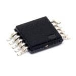
| 封装/箱体 | MSOP-10 |
| 接口类型 | I2C, SPI |
| 最大工作温度 | + 105 C |
| 最小工作温度 | - 40 C |
| 标准包装 | 50 |
| 电压参考 | 2.5 V |
| 电源电压-最大 | 5.5 V |
| 电源电压-最小 | 2.7 V |
| 稳定时间 | 5 ns |
| 类型 | Precision DAC |
| 结构 | Segment |
| 转换器数量 | 1 |
| 输出类型 | Voltage Buffered |
| 配用 | /product-detail/zh/EVAL-AD5693RSDZ/EVAL-AD5693RSDZ-ND/4863483 |


- 商务部:美国ITC正式对集成电路等产品启动337调查
- 曝三星4nm工艺存在良率问题 高通将骁龙8 Gen1或转产台积电
- 太阳诱电将投资9.5亿元在常州建新厂生产MLCC 预计2023年完工
- 英特尔发布欧洲新工厂建设计划 深化IDM 2.0 战略
- 台积电先进制程称霸业界 有大客户加持明年业绩稳了
- 达到5530亿美元!SIA预计今年全球半导体销售额将创下新高
- 英特尔拟将自动驾驶子公司Mobileye上市 估值或超500亿美元
- 三星加码芯片和SET,合并消费电子和移动部门,撤换高东真等 CEO
- 三星电子宣布重大人事变动 还合并消费电子和移动部门
- 海关总署:前11个月进口集成电路产品价值2.52万亿元 增长14.8%


PDF Datasheet 数据手册内容提取
Tiny 16-/14-/12-Bit I2C nanoDAC+, with ±2 LSB INL (16-Bit) and 2 ppm/°C Reference Data Sheet AD5693R/AD5692R/AD5691R/AD5693 FEATURES FUNCTIONAL BLOCK DIAGRAM Ultrasmall package: 2 mm × 2 mm, 8-lead LFCSP VLOGIC VREF VDD High relative accuracy (INL): ±2 LSB maximum at 16 bits AD5693R/AD5692R/AD5691R LDAC PORWEESRE-TON 2R.E5VF AADD55669932RR// Low drift, 2.5 V reference: 2 ppm/°C typical AD5691R Selectable span output: 2.5 V or 5 V REF DAC OUTPUT AD5693 RESET REGISTER 16-/1D4-A/1C2-BIT BUFFER VOUT External reference only Selectable span output: V or 2 × V REF REF INPUT POWER-DOWN Total unadjusted error (TUE): ±0.06% of FSR maximum CONTROL LOGIC CONTROL LOGIC RESISTOR NETWORK Offset error: ±1.5 mV maximum Gain error: ±0.05 % of FSR maximum Low glitch: 0.1 nV-sec SDA SCL A0 GND 12077-001 High drive capability: 20 mA Figure 1. MSOP Low power: 1.2 mW at 3.3 V 1.8 V VLOGIC compatible LDAC OR VLOGIC OR RESET1 VREF VDD Wide operating temperature range: −40°C to +105°C AD5693R/ POWER-ON 2.5V REF2 APPLICATIONS RESET AD5692R/ AD5691R/ Process controls AD5693 REF Data acquisition systems DAC OUTPUT REGISTER 16-/14-/12-BIT BUFFER VOUT Digital gain and offset adjustment DAC Programmable voltage sources Optical modules INPUT POWER-DOWN CONTROL LOGIC CONTROL LOGIC RESISTOR GENERAL DESCRIPTION NETWORK The AD5693R/AD5692R/AD5691R/AD5693, members of the nanoDAC+® family, are low power, single-channel, 16-/14-/12-bit buffered voltage output DACs. The devices, except the AD5693, SDA SCL A0 GND 2in pclpumde/ °aCn denriafbt.l eTdh bey o duetpfauutl st pinatne rcnaanl b2e.5 p Vro rgerfaemremnceed, otoff ebrei n0g V to 12NNOOTT AAVLLA IPLIANBSL AEV IANI LTAHBE LAED I5N6 9A3L.L 8-LEAD LFCSP MODELS. 12077-002 Figure 2. LFCSP V or 0 V to 2 × V . All devices operate from a single 2.7 V to REF REF 5.5 V supply and are guaranteed monotonic by design. The Table 1. Related Devices devices are available in a 2.00 mm × 2.00 mm, 8-lead LFCSP or Interface Reference 16-Bit 14-Bit 12-Bit a 10-lead MSOP. SPI Internal AD5683R AD5682R AD5681R The internal power-on reset circuit ensures that the DAC register External AD5683 is written to zero scale at power-up while the internal output I2C Internal AD5693R AD5692R AD5691R buffer is configured in normal mode. The AD5693R/AD5692R/ External AD5693 AD5691R/AD5693 contain a power-down mode that reduces the PRODUCT HIGHLIGHTS current consumption of the device to 2 µA (maximum) at 5 V and provides software selectable output loads. 1. High relative accuracy (INL): ±2 LSB maximum The AD5693R/AD5692R/AD5691R/AD5693 use an I2C (AD5693R/AD5693, 16-bit). 2. Low drift, 2.5 V on-chip reference: 2 ppm/°C typical and interface. Some device options also include an asynchronous 5 ppm/°C maximum temperature coefficient. RESET pin and a V pin, allowing 1.8 V compatibility. LOGIC 3. 2 mm × 2 mm, 8-lead LFCSP and 10-lead MSOP. Rev. D Document Feedback Information furnished by Analog Devices is believed to be accurate and reliable. However, no responsibility is assumed by Analog Devices for its use, nor for any infringements of patents or other One Technology Way, P.O. Box 9106, Norwood, MA 02062-9106, U.S.A. rights of third parties that may result from its use. Specifications subject to change without notice. No license is granted by implication or otherwise under any patent or patent rights of Analog Devices. Tel: 781.329.4700 ©2014–2017 Analog Devices, Inc. All rights reserved. Trademarks and registered trademarks are the property of their respective owners. Technical Support www.analog.com
AD5693R/AD5692R/AD5691R/AD5693 Data Sheet TABLE OF CONTENTS Features .............................................................................................. 1 Digital-to-Analog Converter .................................................... 19 Applications ....................................................................................... 1 Transfer Function ....................................................................... 19 General Description ......................................................................... 1 DAC Architecture ....................................................................... 19 Functional Block Diagram .............................................................. 1 Serial Interface ................................................................................ 20 Product Highlights ........................................................................... 1 I2C Serial Data Interface ............................................................ 20 Revision History ............................................................................... 2 I2C Address .................................................................................. 20 Specifications ..................................................................................... 3 Write Operation.......................................................................... 20 AC Characteristics ........................................................................ 5 Read Operation........................................................................... 22 Timing Characteristics ................................................................ 5 Load DAC (Hardware LDAC Pin) ........................................... 23 Absolute Maximum Ratings ............................................................ 7 Hardware RESET ........................................................................ 23 Thermal Resistance ...................................................................... 7 Thermal Hysteresis .................................................................... 23 ESD Caution .................................................................................. 7 Power-Up Sequence ................................................................... 23 Pin Configurations and Function Descriptions ........................... 8 Recommended Regulator .......................................................... 24 Typical Performance Characteristics ........................................... 12 Layout Guidelines....................................................................... 24 Terminology .................................................................................... 18 Outline Dimensions ....................................................................... 25 Theory of Operation ...................................................................... 19 Ordering Guide .......................................................................... 26 REVISION HISTORY 2/2017—Rev. C to Rev. D 5/2014—Rev. 0 to Rev. A Changes to Features Section............................................................ 1 Added AD5693 ................................................................... Universal Changes to Specifications Section .................................................. 3 Changes to Features, General Description, Figure 2, Table 1, Changes to V Parameter, Table 2 ............................................ 4 and Product Highlights .................................................................... 1 LOGIC Changes to AC Characteristics Section and Timing Added AD5693 Parameter, Table 1 and AD5693 Parameter, Characteristics Section ..................................................................... 5 Table 1 ................................................................................................. 3 Changes to Table 5 ............................................................................ 7 Changes to Endnote 1, Specifications Section, Table 1 ................ 4 Changes to RESET Pin Description, Table 7................................. 8 Change to Total Harmonic Distortion, AC Characteristics, Changes to RESET Pin Description, Table 10 ............................ 11 Table 3 and Endnote 2, Table 3 ........................................................ 5 Changes to Figure 49 ...................................................................... 22 Changes to Endnote 7, Timing Characteristics, Table 4 .............. 5 Change to Pin 9, Description, Table 7 ............................................ 8 5/2016—Rev. B to Rev. C Changes to Figure 6 and Table 8 ...................................................... 9 Changed V = 1.8 V to 5.5 V to V = 1.8 V − 10% to 5 V + Change to Figure 11 ....................................................................... 10 LOGIC LOGIC 10% .................................................................................. Throughout Change to Figure 18 ....................................................................... 11 Changes to Features Section............................................................ 1 Change to the External Reference Section .................................. 17 Changes to V Parameter, Table 2 ............................................ 4 Change to Figure 46 ....................................................................... 19 LOGIC Changes to Table 7 ............................................................................ 8 Change to Figure 48 ....................................................................... 20 Changes to Table 9 .......................................................................... 10 Change to Figure 50 ....................................................................... 21 Changes to Terminology Section.................................................. 18 Changes to Ordering Guide .......................................................... 23 11/2014—Rev. A to Rev. B 2/2014—Revision 0: Initial Version Changes to Figure 2 .......................................................................... 1 Changes to Table 8 ............................................................................ 9 Change to Figure 7 ......................................................................... 10 Added Table 9; Renumbered Sequentially .................................. 10 Added Figure 8; Renumbered Sequentially, and Table 10 ......... 11 Added Recommended Regulator Section ................................... 24 Changes to Ordering Guide .......................................................... 26 Rev. D | Page 2 of 26
Data Sheet AD5693R/AD5692R/AD5691R/AD5693 SPECIFICATIONS V = 2.7 V to 5.5 V, R = 2 kΩ to GND, C = 200 pF to GND, V = 2.5 V to V − 0.2 V, V = 1.62 V to 5.5 V, −40°C < T < +105°C, DD L L REF DD LOGIC A unless otherwise noted. Table 2. Parameter Min Typ Max Unit Test Conditions/Comments STATIC PERFORMANCE1 AD5693R Resolution 16 Bits Relative Accuracy (INL) A Grade ±8 LSB B Grade ±2 LSB Gain = 2 ±3 LSB Gain = 1 Differential Nonlinearity ±1 LSB Guaranteed monotonic by design AD5692R Resolution 14 Bits Relative Accuracy ±4 LSB Differential Nonlinearity ±1 LSB Guaranteed monotonic by design AD5691R Resolution 12 Bits Relative Accuracy A Grade ±2 LSB B Grade ±1 LSB Differential Nonlinearity ±1 LSB Guaranteed monotonic by design AD5693 Resolution 16 Bits Relative Accuracy (INL) ±2 LSB Gain = 2 ±3 LSB Gain = 1 Differential Nonlinearity ±1 LSB Guaranteed monotonic by design Zero Code Error 1.25 mV All 0s loaded to DAC register Offset Error ±1.5 mV Full-Scale Error ±0.075 % of FSR All 1s loaded to DAC register Gain Error ±0.05 % of FSR Total Unadjusted Error ±0.16 % of FSR Internal reference, gain = 1 ±0.14 % of FSR Internal reference, gain = 2 ±0.075 % of FSR External reference, gain = 1 ±0.06 % of FSR External reference, gain = 2 Zero Code Error Drift ±1 µV/°C Offset Error Drift ±1 µV/°C Gain Temperature Coefficient ±1 ppm/°C DC Power Supply Rejection Ratio 0.2 mV/V DAC code = midscale, V = 5 V ±10% DD OUTPUT CHARACTERISTICS Output Voltage Range 0 V V Gain = 0 REF 0 2 × V V Gain = 1 REF Capacitive Load Stability 2 nF R = ∞ L 10 nF R = 2 kΩ L Resistive Load 1 kΩ C = 0 µF L Load Regulation 10 µV/mA V = 5 V, DAC code = midscale, −30 mA ≤ I ≤ +30 mA DD OUT 10 µV/mA V = 3 V, DAC code = midscale, −20 mA ≤ I ≤ +20 mA DD OUT Short-Circuit Current 20 50 mA Load Impedance at Rails2 20 Ω Rev. D | Page 3 of 26
AD5693R/AD5692R/AD5691R/AD5693 Data Sheet Parameter Min Typ Max Unit Test Conditions/Comments REFERENCE OUTPUT Output Voltage 2.4975 2.5025 V At ambient temperature Voltage Reference TC3 See the Terminology section A Grade 5 20 ppm/°C B Grade 2 5 ppm/°C Output Impedance 0.05 Ω Output Voltage Noise 16.5 µV p-p 0.1 Hz to 10 Hz Output Voltage Noise Density 240 nV/√Hz At ambient temperature, f = 10 kHz, C = 10 nF L Capacitive Load Stability 5 µF R = 2 kΩ L Load Regulation Sourcing 50 µV/mA At ambient temperature, V ≥ 3 V DD Load Regulation Sinking 30 µV/mA At ambient temperature Output Current Load Capability ±5 mA V ≥ 3 V DD Line Regulation 80 µV/V At ambient temperature Thermal Hysteresis 125 ppm First cycle 25 ppm Additional cycles REFERENCE INPUT Reference Current 35 µA V = V = V = 5.5 V, gain = 1 REF DD LOGIC 57 µA V = V = V = 5.5 V, gain = 2 REF DD LOGIC Reference Input Range4 V V DD Reference Input Impedance 120 kΩ Gain = 1 60 kΩ Gain = 2 LOGIC INPUTS IIN, Input Current ±1 µA Per pin ±3 µA SDA and SCL pins V , Input Low Voltage4 0.3 × V V INL DD V , Input High Voltage4 0.7 × V V INH DD C , Pin Capacitance 2 pF IN LOGIC OUTPUTS (SDA)4 Output Low Voltage, V 0.4 V I = 200 μA OL SINK Output High Voltage, V V − 0.4 V I = 200 μA OH DD SOURCE Pin Capacitance 4 pF POWER REQUIREMENTS V 5 1.62 5.5 V LOGIC I 5 0.25 3 µA V = V or V = GND LOGIC IH LOGIC IL V 2.7 5.5 V Gain = 1 DD V + 1.5 5.5 V Gain = 2 REF I 6 V = V , V = GND DD IH DD IL Normal Mode7 350 500 µA Internal reference enabled 110 180 µA Internal reference disabled Power-Down Modes8 2 µA 1 Linearity calculated using a reduced code range: AD5693R/AD5693 (Code 512 to Code 65,535); AD5692R (Code 128 to Code 16,384); AD5691R (Code 32 to Code 4096). Output unloaded. 2 When drawing a load current at either rail, the output voltage headroom, with respect to that rail, is limited by the 20 Ω typical channel resistance of the output devices; for example, when sinking 1 mA, the minimum output voltage with 20 Ω, 1 mA generates 20 mV. See Figure 36 for more details. 3 Voltage reference temperature coefficient is calculated as per the box method. See the Terminology section for more information. 4 Substitute VLOGIC for VDD if the device includes a VLOGIC pin. 5 The VLOGIC pin is not available on all models. 6 If the VLOGIC pin is not available, IDD = IDD + ILOGIC. 7 Interface inactive. DAC active. DAC output unloaded. 8 DAC powered down. Rev. D | Page 4 of 26
Data Sheet AD5693R/AD5692R/AD5691R/AD5693 AC CHARACTERISTICS V = 2.7 V to 5.5 V, R = 2 kΩ to GND, C = 200 pF to GND, V = 2.5 V to V − 0.2 V, V = 1.62 V to 5.5 V, −40°C < T < +105°C, DD L L REF DD LOGIC A typical at 25°C, unless otherwise noted. Table 3. Parameter Typ Max Unit Conditions/Comments Output Voltage Settling Time1, 2 5 7 µs Gain = 1 Slew Rate 0.7 V/µs Digital-to-Analog Glitch Impulse1 0.1 nV-s ±1 LSB change around major carry, gain = 2 Digital Feedthrough1 0.1 nV-s Total Harmonic Distortion1 −80 dB At ambient temperature, BW = 20 kHz, V = 5 V, f = 1 kHz DD OUT Output Noise Spectral Density1 300 nV/√Hz DAC code = midscale, 10 kHz Output Noise 6 µV p-p 0.1 Hz to 10 Hz; internal reference SNR 90 dB At ambient temperature, bandwidth (BW) = 20 kHz, V =5 V, f = 1 kHz DD OUT SFDR 83 dB At ambient temperature, BW = 20 kHz, V =5 V, f = 1 kHz DD OUT SINAD 80 dB At ambient temperature, BW = 20 kHz, V =5 V, f = 1 kHz DD OUT 1 See the Terminology section. 2 For the AD5693R/AD5693, to ±2 LSB. For the AD5692R, to ±1 LSB. For the AD5691R, to ±0.5 LSB TIMING CHARACTERISTICS V = 2.7 V to 5.5 V, V = 1.62 V to 5.5 V, −40°C < T < +105°C, unless otherwise noted. DD LOGIC A Table 4. Parameter1 Min Typ Max Unit Description f 2 400 kHz Serial clock frequency SCL t 0.6 µs SCL high time, t 1 HIGH t 1.3 µs SCL low time, t 2 LOW t 100 ns Data setup time, t 3 SU; DAT t 3 0 0.9 µs Data hold time, t 4 HD; DAT t 0.6 µs Setup time for a repeated start condition, t 5 SU; STA t 0.6 µs Hold time (repeated) start condition, t 6 HD; STA t 1.3 µs Bus free time between a stop and a start condition, t 7 BUF t 0.6 µs Setup time for a stop condition, t 8 SU; STO t 20 300 ns Rise time of SDA signal, t 9 r t 4 20 × (V /5.5 V) 300 ns Fall time of SDA signal, t 10 DD f t 20 300 ns Rise time of SCL signal, t 11 r t 4 20 × (V /5.5 V) 300 ns Fall time of SCL signal, t 12 DD f t 5 0 50 ns Pulse width of suppressed spike (not shown in Figure 3) SP t13 400 ns LDAC falling edge to SCL falling edge t14 400 ns LDAC pulse width (synchronous mode) t15 20 ns LDAC pulse width (asynchronous mode) t16 75 ns RESET pulse width t 6 600 µs Reference power-up (not shown in Figure 3) REF_POWER_UP t 7 6 µs Exit shutdown (not shown in Figure 3) SHUTDOWN 1 Maximum bus capacitance is limited to 400 pF. All input signals are specified with tR = tF = 1 ns/V (10% to 90% of VDD) and timed from a voltage level of (VIL + VIH)/2. 2 The SDA and SCL timing is measured with the input filters enabled. Switching off the input filters improves the transfer rate; however, it has a negative effect on the EMC behavior of the device. 3 The master should add at least 300 ns for the SDA signal (with respect to the VOH (min) of the SCL signal) to bridge the undefined region of the falling edge of SCL. 4 Substitute VLOGIC for VDD on devices that include a VLOGIC pin. 5 Not applicable for standard mode. 6 Expect the same timing when powering up the device after VDD is equal to 2.7 V. 7 Time to exit power-down to normal mode of AD5693R/AD5692R/AD5691R/AD5693 operation. Rev. D | Page 5 of 26
AD5693R/AD5692R/AD5691R/AD5693 Data Sheet Timing Diagrams t12 t11 t6 t8 t 2 SCL t10 t9 t1 t5 t t 3 4 SDA t 7 START REPEAT START STOP RECPOENAODTRI TSITOANRT CONDITION CONDITION 12077-003 Figure 3. I2C Serial Interface Timing Diagram SCL SDA ACK STOP CONDITION t 14 t t 13 15 LDAC SYNCHRONOUS ASYNCHRONOUS DAC UPDATE DAC UPDATE t 16 RESET 12077-004 Figure 4. I2C RESET and LDAC Timing Rev. D | Page 6 of 26
Data Sheet AD5693R/AD5692R/AD5691R/AD5693 ABSOLUTE MAXIMUM RATINGS T = 25°C, unless otherwise noted. THERMAL RESISTANCE A θ is defined by the JEDEC JESD51 standard, and the value is Table 5. JA dependent on the test board and test environment. Parameter Rating VDD to GND −0.3 V to +7 V Table 6. Thermal Resistance1 V to GND −0.3 V to +7 V LOGIC Package Type θ θ Unit JA JC V to GND −0.3 V to V + 0.3 V or +7 V OUT DD 8-Lead LFCSP 90 25 °C/W (whichever is less) 10-Lead MSOP 135 N/A °C/W V to GND −0.3 V to V + 0.3 V or +7 V REF DD (whichever is less) 1 JEDEC 2S2P test board, still air (0 m/sec airflow). Digital Input Voltage to GND1 −0.3 V to VDD + 0.3 V or +7 V (whichever is less) ESD CAUTION Operating Temperature Range Industrial −40°C to +105°C Storage Temperature Range −65°C to +150°C Junction Temperature (T max) 135°C J Power Dissipation (TJ max − TA)/θJA 1 Substitute VDD with VLOGIC on devices that include a VLOGIC pin. Stresses at or above those listed under Absolute Maximum Ratings may cause permanent damage to the product. This is a stress rating only; functional operation of the product at these or any other conditions above those indicated in the operational section of this specification is not implied. Operation beyond the maximum operating conditions for extended periods may affect product reliability. Rev. D | Page 7 of 26
AD5693R/AD5692R/AD5691R/AD5693 Data Sheet PIN CONFIGURATIONS AND FUNCTION DESCRIPTIONS VDD 1 10 VOUT VLOGIC 2 AD5693R/ 9 VREF AD5691R RESET 3 8 SDA TOP VIEW LGDANCD 45 (Not to Scale) 76 SAC0L 12077-005 Figure 5. AD5693R/AD5691R Pin Configuration, 10-Lead MSOP Table 7. AD5693R/AD5691R Pin Function Descriptions, 10-Lead MSOP Pin No. Mnemonic Description 1 V Power Supply Input. These devices can be operated from 2.7 V to 5.5 V. Decouple the supply to GND. DD 2 V Digital Power Supply. Voltage ranges from 1.62 V to 5.5 V. Decouple the supply to GND. LOGIC 3 RESET Hardware Reset Pin. The RESET input is low level sensitive. When RESET is low, the device is reset and external pins are ignored. The input and DAC registers are loaded with zero code value and control register loaded with default values. Tie this pin to V if not used. If this pin is forced low at power-up, the power-on reset (POR) LOGIC circuit does not initialize the device correctly until this pin is released. 4 LDAC Load DAC. Transfers the content of the input register to the DAC register. It can be operated in two modes, asynchronously and synchronously, as shown in Figure 4. This pin can be tied permanently low, and the DAC updates when new data is written to the input register. 5 GND Ground Reference. 6 A0 Programmable Address for Multiple Package Decoding. The address pin can be updated on-the-fly. 7 SCL Serial Clock Line. 8 SDA Serial Data Input/Output. 9 V Reference Input/Output. In the AD5693R/AD5691R, this is a reference output pin by default. It is recommended REF to use a 10 nF decoupling capacitor for the internal reference. 10 V Analog Output Voltage from the DAC. The output amplifier has rail-to-rail operation. OUT Rev. D | Page 8 of 26
Data Sheet AD5693R/AD5692R/AD5691R/AD5693 VDD 1 AD5693R/ 8 VOUT AD5692R/ LDAC 2 AD5691R/ 7 VREF AD5693 GND 3 6 SDA TOP VIEW (Not to Scale) A0 4 5 SCL N1.O CTOENSNECT THE EXPOSED PAD TO GND. 12077-006 Figure 6. AD5693R/AD5692R/AD5691R/AD5693 Pin Configuration, 8-Lead LFCSP, LDAC Option Table 8. AD5693R/AD5692R/AD5691R/AD5693 Pin Function Descriptions, 8-Lead LFCSP, LDAC Option Pin No. Mnemonic Description 1 V Power Supply Input. These devices can be operated from 2.7 V to 5.5 V. Decouple the supply to GND. DD 2 LDAC Load DAC. Transfers the content of the input register to the DAC register. It can be operated in two modes, asynchronously and synchronously, as shown in Figure 4. This pin can be tied permanently low and the DAC updates when new data is written to the input register. 3 GND Ground Reference. 4 A0 Programmable Address for Multiple Package Decoding. The address pin can be updated on-the-fly. 5 SCL Serial Clock Line. 6 SDA Serial Data Input/Output. 7 V Reference Input/Output. In the AD5693R/AD5692R/AD5691R, this is a reference output pin by default. In the AD5693, REF this pin is a reference input only. It is recommended to use a 10 nF decoupling capacitor for the internal reference. 8 V Analog Output Voltage from the DAC. The output amplifier has rail-to-rail operation. OUT EPAD Exposed Pad. Connect the exposed pad to GND. Rev. D | Page 9 of 26
AD5693R/AD5692R/AD5691R/AD5693 Data Sheet VDD 1 8 VOUT VLOGIC 2 AD5693R-1 7 VREF AD5691R-1 GND 3 6 SDA TOP VIEW (Not to Scale) A0 4 5 SCL N1.O CTOENSNECT THE EXPOSED PAD TO GND. 12077-007 Figure 7. AD5693R-1/AD5691R-1 Pin Configuration, 8-Lead LFCSP, VLOGIC Option Table 9. AD5693R-1/AD5691R-1 Pin Function Descriptions, 8-Lead LFCSP, V Option LOGIC Pin No. Mnemonic Description 1 V Power Supply Input. These devices can be operated from 2.7 V to 5.5 V. Decouple the supply to GND. DD 2 V Digital Power Supply. Voltage ranges from 1.62 V to 5.5 V. Decouple the supply to GND. LOGIC 3 GND Ground Reference. 4 A0 Programmable Address for Multiple Package Decoding. The address pin can be updated on-the-fly. 5 SCL Serial Clock Line. 6 SDA Serial Data Input/Output. 7 V Reference Input/Output. In the AD5693R-1/AD5691R-1, this is a reference output pin by default. It is REF recommended to use a 10 nF decoupling capacitor for the internal reference. 8 V Analog Output Voltage from the DAC. The output amplifier has rail-to-rail operation. OUT EPAD Exposed Pad. Connect the exposed pad to GND. Rev. D | Page 10 of 26
Data Sheet AD5693R/AD5692R/AD5691R/AD5693 VDD 1 8 VOUT RESET 2 AD5693R-2 7 VREF GND 3 6 SDA TOP VIEW (Not to Scale) A0 4 5 SCL N1.O CTOENSNECT THE EXPOSED PAD TO GND. 12077-107 Figure 8. AD5693R-2 Pin Configuration, 8-Lead LFCSP, RESET Option Table 10. AD5693R-2 Pin Function Descriptions, 8-Lead LFCSP, RESET Option Pin No. Mnemonic Description 1 V Power Supply Input. These devices can be operated from 2.7 V to 5.5 V. Decouple the supply to GND. DD 2 RESET Hardware Reset Pin. The RESET input is low level sensitive. When RESET is low, the device is reset and external pins are ignored. The input and DAC registers are loaded with zero code value and the control register is loaded with default values. Tie this pin to V if not used. If this pin is forced low at power-up, the power-on reset (POR) circuit DD does not initialize the device correctly until this pin is released. 3 GND Ground Reference. 4 A0 Programmable Address for Multiple Package Decoding. The address pin can be updated on-the-fly. 5 SCL Serial Clock Line. 6 SDA Serial Data Input/Output. 7 V Reference Input/Output. In the AD5693R-2, this is a reference output pin by default. It is recommended to use a REF 10 nF decoupling capacitor for the internal reference. 8 V Analog Output Voltage from the DAC. The output amplifier has rail-to-rail operation. OUT EPAD Exposed Pad. Connect the exposed pad to GND. Rev. D | Page 11 of 26
AD5693R/AD5692R/AD5691R/AD5693 Data Sheet TYPICAL PERFORMANCE CHARACTERISTICS 2 2 VDD = 5V VDD = 5V TA = 25°C TA = 25°C VREF = 2.5V VREF = 2.5V 1 1 B) B) NL (LS 0 NL (LS 0 I D –1 –1 –20 10000 20000 300C0O0DE40000 50000 6000065535 12077-009 –20 10000 20000 300C0O0DE40000 50000 6000065535 12077-012 Figure 9. AD5693R/AD5693 INL Figure 12. AD5693R/AD5693 DNL 2 1.0 VDD = 5V VDD = 5V TA = 25°C 0.8 TA = 25°C VREF = 2.5V VREF = 2.5V 0.6 1 0.4 B) B) 0.2 NL (LS 0 NL (LS 0 I D–0.2 –0.4 –1 –0.6 –0.8 –20 2000 4000 6000 8C0O0D0E10000 12000 14000 16383 12077-010 –1.00 2000 4000 6000 8C0O0D0E10000 12000 14000 16383 12077-013 Figure 10. AD5692R INL Figure 13. AD5692R DNL 2.0 1.0 VDD = 5V VDD = 5V 1.5 TVAR E=F 2=5 °2C.5V 0.8 TVAR E=F 2=5 °2C.5V 0.6 1.0 0.4 0.5 B) B) 0.2 NL (LS 0 NL (LS 0 I D–0.2 –0.5 –0.4 –1.0 –0.6 –1.5 –0.8 –2.00 500 1000 1500 2C0O00DE2500 3000 3500 4000 12077-011 –1.00 500 1000 1500 2C0O00DE2500 3000 3500 4000 12077-014 Figure 11. AD5691R INL Figure 14. AD5691R DNL Rev. D | Page 12 of 26
Data Sheet AD5693R/AD5692R/AD5691R/AD5693 1.2 1.4 VDD = 5V U1_DNL U2_DNL VDD = 5V VREF = 2.5V U3_DNL U1_INL TA = 25°C 1.0 1.2 U2_INL U3_INL B) B) 1.0 S 0.8 S L L OR ( OR ( 0.8 R 0.6 R R R DNL E 0.4 UU13__DDNNLL__IINNTT__RREEFF UU21__DDNNLL__EINXTT__RREEFF DNL E 0.6 ND UU21__DINNLL__INETX_TR_ERFEF UU32__DINNLL__INETX_TR_ERFEF ND 0.4 A U3_INL_INT_REF U1_INL_EXT_REF A L 0.2 U2_INL_EXT_REF U3_INL_EXT_REF L N N 0.2 I I 0 0 –0.2 –40 –20 0 TEMP2E0RATU4R0E (°C)60 80 105 12077-015 –0.22 3 VREF (V) 4 5 12077-018 Figure 15. INL and DNL Error vs. Temperature (AD5693R/AD5693) Figure 18. INL and DNL Error vs. VREF (AD5693R/AD5693) 1.4 0.02 U1_DNL_INT_REF U2_DNL_INT_REF TA = 25°C (AD5693R/AD5693) U3_DNL_INT_REF U1_DNL_EXT_REF (AD5692R) 1.2 UU21__DINNLL__INETX_TR_REFEF UU32__DINNLL__INETX_TR_REFEF (AD5691R) U3_INL_INT_REF U1_INL_EXT_REF 0.01 B) 1.0 U2_INL_EXT_REF U3_INL_EXT_REF S L D DNL ERROR ( 000...468 TUE (% FSR)–0.010 N A –0.02 L N 0.2 I –0.03 0 –0.2 –0.04 2.70 3.30 3.75 VDD 4(V.2)5 4.75 5.25 12077-016 000 120500000000 2410000000000 3610050C00000O0DE4820000000000 15200500000000 1632000000000016465035983535 12077-019 Figure 16. INL and DNL Error vs. VDD Figure 19. TUE vs. Code 0.06 0.04 U1_EXT_REF VDD = 5V TA = 25°C U2_EXT_REF GAIN = 1 GAIN = 1 UU31__EINXTT__RREEFF VREF = 2.5V 0.03 VREF = 2.5V 0.04 U2_INT_REF U3_INT_REF 0.02 R) 0.02 R) S S F F % % 0.01 E ( E ( TU 0 TU 0 –0.02 –0.01 U1_INT_REF U1_EXT_REF U2_INT_REF U2_EXT_REF U3_INT_REF U3_EXT_REF –0.04 –40 0 TEMPERATUR40E (°C) 80 12077-017 –0.02 2.70 3.30 3.75 VDD 4(V.2)5 4.75 5.25 12077-020 Figure 17. TUE vs. Temperature Figure 20. TUE vs. VDD Rev. D | Page 13 of 26
AD5693R/AD5692R/AD5691R/AD5693 Data Sheet 0.03 0.030 TA = 25°C 0.025 GAIN = 1 0.02 VREF = 2.5V 0.020 0.01 0.015 R) R) 0.010 S S F 0 F % % 0.005 ROR (–0.01 ROR ( 0 ER ER–0.005 U1_INT_REF –0.02 U2_INT_REF –0.010 U3_INT_REF –0.015 –0.03 U1_EXT_REF VDD = 5V U1_INT_REF U1_EXT_REF U2_EXT_REF GAIN = 1 –0.020 U2_INT_REF U2_EXT_REF U3_EXT_REF VREF = 2.5V U3_INT_REF U3_EXT_REF –0.04 –40 0 TEMPERATUR40E (°C) 80 12077-021 –0.025 2.70 3.30 3.75 VD4D.2 5(V) 4.75 5.25 5.50 12077-024 Figure 21. Gain Error and Full-Scale Error vs. Temperature Figure 24. Gain Error and Full-Scale Error vs. VDD 350 500 VDD = 5V U1_INT_REF TA = 25°C GAIN = 1 U2_INT_REF GAIN = 1 300 VREF = 2.5V U3_INT_REF VREF = 2.5V 400 U1_EXT_REF U2_EXT_REF 250 U3_EXT_REF R (µV) 200 R (µV) 300 O O RR 150 RR E E 200 100 U1_INT_REF U2_INT_REF U3_INT_REF 100 50 U1_EXT_REF U2_EXT_REF U3_EXT_REF 0 –40 –20 0 TEMP2E0RATU4R0E (°C)60 80 105 12077-022 0 2.70 3.30 3.75 VD4D.2 5(V) 4.75 5.25 5.50 12077-025 Figure 22. Zero Code Error and Offset Error vs. Temperature Figure 25. Zero Code Error and Offset Error vs. VDD 2.505 4.5 U1 VDD = 5V VDD = 5V U2 4.0 TA = 25°C U3 GAIN = 1 2.503 3.5 S 3.0 T 2.501 HI V) F 2.5 (EF R O VR BE 2.0 2.499 M U N 1.5 1.0 2.497 0.5 2.495–40 1T0EMPERATURE (°C)60 12077-023 02.500012.500042.500072.500102.500132.500162.500192.500222.500252.500282.500312.500342.500372.500402.50043V2.50046R2.50049EF2.50052 (2.50055V)2.500582.500612.500642.500672.500702.500732.500762.500792.500822.500852.500882.500912.500942.500972.50100 12077-026 Figure 23. Internal Reference Voltage vs. Temperature (Grade B) Figure 26. Reference Output Spread Rev. D | Page 14 of 26
Data Sheet AD5693R/AD5692R/AD5691R/AD5693 2.50015 2.5009 TA = 25°C TA = 25°C 5.5V 5.0V 2.50010 3.0V 2.5008 2.7V 2.50005 2.5007 V) 2.50000 V) V (REF2.49995 V (REF 2.5006 2.5005 2.49990 D11 2.5004 2.49985 D12 D13 2.499802.5 3.5 VDD (V) 4.5 5.5 12077-027 2.500–30.005 –0.003 L–O0.A0D01 CURRE0N.T00 (1A) 0.003 0.005 12077-030 Figure 27. Internal Reference Voltage vs. VDD Figure 30. Internal Reference Voltage vs. Load Current 1800 T TA = 25°C VDD = 5V VDD = 5V 1600 TA = 25°C Hz) V/√ 1400 n D ( 1200 S N CE 1000 1 N E ER 800 F E L R 600 A N R 400 E T N I 200 CH1 10µV M1.00s A CH1 2.00µV 12077-028 010 100 FR1kEQUENCY 1(H0kz) 100k 1M 12077-031 Figure 28. Internal Reference Noise, 0.1 Hz to 10 Hz Figure 31. Internal Reference Noise Spectral Density vs. Frequency T TA = 25°C T TA = 25°C VDD = 5V VDD = 5V 1 1 CH1 10µV M1.00s A CH1 2.00µV 12077-029 CH1 10µV M1.00s A CH1 2.00µV 12077-032 Figure 29. 0.1 Hz to 10 Hz Output Noise Plot, Internal Reference On Figure 32. 0.1 Hz to 10 Hz Output Noise Plot, External Reference Rev. D | Page 15 of 26
AD5693R/AD5692R/AD5691R/AD5693 Data Sheet 1200 1.4 1000 FMZUEIDRLSLOC-SSACCLAAELLEE VTGADA DI=N =2 =55 °V1C 1.0 SSSIOINNUKKRIINNCGGIN,, GVV,DD VDD D==D 35 =VV 5V TA = 25°C SOURCING, VDD = 3V 0.6 800 nV/√Hz) 600 (V)UT 0.2 SD ( ΔVO–0.2 N 400 –0.6 200 –1.0 010 100 FR1kEQUENCY 1(H0kz) 100k 1M 12077-033 –1.40 0.0L1OAD CURRENT (A0).02 0.03 12077-036 Figure 33. Noise Spectral Density vs. Frequency, Gain = 1 Figure 36. Headroom/Footroom vs. Load Current 6 7 0xFFFF VDD = 5V 0xFFFF VDD = 5V 5 00xxC8000000 TGAA I=N 2 =5 °1C 6 00xxC8000000 TGAA I=N 2 =5 °2C 0x4000 0x4000 0x0000 5 0x0000 4 4 V) 3 V) 3 (UT (UT VO 2 VO 2 1 1 0 0 –1 –1–50 LOAD CUR0RENT (mA) 50 12077-034 –2–50 LOAD CUR0RENT (mA) 50 12077-037 Figure 34. Source and Sink Capability, Gain = 1 Figure 37. Source and Sink Capability, Gain = 2 500 0.0015 VDD = 5V GAIN = 1 VDD = 5V 450 0.0010 GAIN = 2 TA = 25°C REFERENCE = 2.5V 400 CODE = 0x7FFF TO 0x8000 0.0005 350 300 0 A) ZS_INT_REF_GAIN = 1 ZS_INT_REF_GAIN = 2 V) (µD250 FS_EXT_REF_GAIN = 2 FS_INT_REF_GAIN = 1 (UT–0.0005 ID200 FS_INT_REF_GAIN = 2 FS_EXT_REF_GAIN = 1 VO –0.0010 150 –0.0015 100 50 –0.0020 0 –40 –20 0 TEMP2E0RATU4R0E (°C)60 80 105 12077-035 –0.00250 1 2 3TIME (µs4) 5 6 7 12077-038 Figure 35. IDD vs. Temperature Figure 38. Digital-to-Analog Glitch Impulse Rev. D | Page 16 of 26
Data Sheet AD5693R/AD5692R/AD5691R/AD5693 2.5 4.5 0nF 0nF 0.2nF 4.0 0.2nF 1nF 1nF 2.0 4.7nF 3.5 4.7nF 10nF 10nF 3.0 1.5 V) V) 2.5 (UT (UT VO VO 2.0 1.0 1.5 0.5 VTAD D= =2 55°VC 1.0 VTAD D= =2 55°VC GAIN = 1 GAIN = 2 0.5 RL = 2kΩ RL = 2kΩ INTERNAL REFERENCE = 2.5V INTERNAL REFERENCE = 2.5V 00 TIM0E.0 (1ms) 0.02 12077-039 00 TIM0E.0 (1ms) 0.02 12077-042 Figure 39. Capacitive Load vs. Settling Time, Gain = 1 Figure 42. Capacitive Load vs. Settling Time, Gain = 2 20 0 VDD = 5V GAIN = 2 TA = 25°C GAIN = 1 V) INTERNAL REFERENCE = 2.5V –10 B d N ( –30 –20 O RTI B) O d –30 ST H ( C DI –80 WIDT –40 NI D O N M A –50 R B A H L –130 –60 A OT VDD = 5V T –70 TA = 25°C VOUT = MIDSCALE EXTERNAL REFERENCE = 2.5V, ±0.1V p-p –1800 5 FREQUE1N0CY (kHz) 15 20 12077-040 –801k 10k FREQU1E0N0kCY (Hz) 1M 10M 12077-043 Figure 40. Total Harmonic Distortion at 1 kHz Figure 43. Multiplying Bandwidth, External Reference = 2.5 V, ±0.1 V p-p, 10 kHz to 10 MHz 6 0.06 3 VDD = 5V TA = 25°C MIDSCALE, GAIN = 2 5 0.05 4 0.04 2 VDD V (V)DD 32 00..0032 V (V)OUT V (V)OUT SYNC MIDSCALE, GAIN = 1 1 1 0.01 VOUT 0 0 –10 1 2 3 TIME4 (ms) 5 6 7 8–0.01 12077-041 0–5 0 TIME5 (µs) 10 15 12077-044 Figure 41. Power-On Reset to 0 V Figure 44. Exiting Power-Down to Midscale Rev. D | Page 17 of 26
AD5693R/AD5692R/AD5691R/AD5693 Data Sheet TERMINOLOGY Relative Accuracy or Integral Nonlinearity (INL) Output Voltage Settling Time For the DAC, relative accuracy or integral nonlinearity is a This is the amount of time it takes for the output of a DAC to measurement of the maximum deviation, in LSBs, from a settle to a specified level for a ¼ to ¾ full-scale input change. straight line passing through the endpoints of the DAC transfer Digital-to-Analog Glitch Impulse function. For typical INL vs. code plots, see Figure 9, Figure 10, Digital-to-analog glitch impulse is the impulse injected into the and Figure 11. analog output when the input code in the DAC register changes Differential Nonlinearity (DNL) state. It is normally specified as the area of the glitch in nV-sec, Differential nonlinearity is the difference between the measured and is measured when the digital input code is changed by change and the ideal 1 LSB change between any two adjacent codes. 1 LSB at the major carry transition (0x7FFF to 0x8000) A specified differential nonlinearity of ±1 LSB maximum ensures Digital Feedthrough monotonicity. This DAC is guaranteed monotonic by design. For Digital feedthrough is a measure of the impulse injected into typical DNL vs. code plots, see Figure 12, Figure 13, and Figure 14. the analog output of the DAC from the digital inputs of the Zero Code Error DAC, but is measured when the DAC output is not updated. It Zero code error is a measurement of the output error when zero is specified in nV-sec, and measured with a full-scale code change code (0x0000) is loaded to the DAC register. Ideally, the output on the data bus, that is, from all 0s to all 1s and vice versa. is 0 V. The zero code error is always positive in the AD5693R/ Noise Spectral Density AD5692R/AD5691R/AD5693 because the output of the DAC Noise spectral density is a measurement of the internally cannot go below 0 V due to a combination of the offset errors in generated random noise. Random noise is characterized as a the DAC and the output amplifier. Zero code error is expressed spectral density (nV/√Hz). It is measured by loading the DAC to in mV. For plots of zero code error, see in Figure 22 and Figure 25. midscale and measuring noise at the output. It is measured in Full-Scale Error nV/√Hz. For plots of noise spectral density, see Figure 29, Full-scale error is a measurement of the output error when Figure 32, and Figure 33. The noise spectral density for the full-scale code (0xFFFF) is loaded to the DAC register. Ideally, reference is shown in Figure 28 and Figure 31. the output is V − 1 LSB or |2 × V | − 1 LSB. Full-scale error is REF REF Multiplying Bandwidth expressed in percent of full-scale range. For plots of full-scale error The amplifiers within the DAC have a finite bandwidth. The vs. temperature, see Figure 21 and Figure 24. multiplying bandwidth is a measure of these finite bandwidths. A Gain Error sine wave on the reference (with full-scale code loaded to the DAC) Gain error is a measure of the span error of the DAC. It is the appears on the output. The multiplying bandwidth is the frequency deviation in slope of the DAC transfer characteristic from the at which the output amplitude falls to 3 dB below the input. ideal expressed as % of FSR. Total Harmonic Distortion (THD) Zero Code Error Drift THD is the difference between an ideal sine wave and its attenuated Zero code error drift is a measurement of the change in zero version using the DAC. The sine wave is used as the reference code error with a change in temperature. It is expressed in µV/°C. for the DAC, and THD is a measurement of the harmonics present on the DAC output. It is measured in dB. Gain Temperature Coefficient Gain temperature coefficient is a measurement of the change in gain Voltage Reference Temperature Coefficient (TC) error with changes in temperature. It is expressed in ppm of FSR/°C. Voltage reference TC is a measure of the change in the reference output voltage with a change in temperature. The reference TC Offset Error is calculated using the box method, which defines the TC as the Offset error is a measure of the difference between V (actual) OUT maximum change in the reference output over a given tempera- and V (ideal) expressed in mV in the linear region of the OUT ture range expressed in ppm/°C as follows: transfer function. Offset error is measured on the AD5693R with Code 512 loaded in the DAC register (Code 256 for the AD5692R V −V and Code 128 for the AD5693R/AD5693). It can be negative or TC= REFmax REFmin ×106 positive. VREFnom×TempRange where: DC Power Supply Rejection Ratio (PSRR) V is the maximum reference output measured over the PSRR indicates how the output of the DAC is affected by changes REFmax total temperature range. in the supply voltage. PSRR is the ratio of the change in V to OUT V is the minimum reference output measured over the total a change in V for full-scale output of the DAC. It is measured REFmin DD temperature range. in mV/V. V is held at 2 V, and V is varied by ±10%. REF DD V is the nominal reference output voltage, 2.5 V. REFnom TempRange is the specified temperature range, −40°C to +105°C. Rev. D | Page 18 of 26
Data Sheet AD5693R/AD5692R/AD5691R/AD5693 THEORY OF OPERATION DIGITAL-TO-ANALOG CONVERTER Because each resistance in the string has same value, R, the The AD5693R/AD5692R/AD5691R/AD5693 are single 16-bit, string DAC is guaranteed monotonic. 14-bit, and 12-bit, serial input, voltage output DACs with a 2.5 V VREF internal reference. The devices operate from supply voltages of 2.7 V to 5.5 V. Data is written to the AD5693R/AD5692R/AD5691R/ R AD5693 in a 24-bit word format via an I2C serial interface. The AD5693R/AD5692R/AD5691R/AD5693 incorporate a R power-on reset circuit that ensures that the DAC output powers up to zero scale. The devices also have a software power-down mode R TO OUTPUT BUFFER that reduces the current consumption to 2 µA maximum. TRANSFER FUNCTION The internal reference is on by default. The input coding to the DAC is straight binary. The ideal output voltage is given by the R following equations: For the AD5693R/AD5693, R VOUT(D) = Gain × VREF × D 12077-046 65,536 Figure 46. Simplified Resistor String Structure For the AD5692R, Internal Reference D The AD5693R/AD5692R/AD5691R on-chip reference is on at VOUT(D) = Gain × VREF × power-up but can be disabled via a write to the control register. 16,384 The AD5693R/AD5692R/AD5691R each have a 2.5 V, 2 ppm/°C For the AD5691R, reference, giving a full-scale output of 2.5 V or 5 V, depending V (D) = Gain × V × D on the state of the gain bit. OUT REF 4096 The internal reference is available at the VREF pin. It is internally buffered and capable of driving external loads of up to 5 mA. where: External Reference D is the decimal equivalent of the binary code that is loaded to the DAC register. The VREF pin is an input pin in the AD5693. The VREF pin can also Gain is the gain of the output amplifier and it is set to ×1 by be configured as an input pin on the AD5693R/AD5692R/ default. The gain can also be set to ×2 using the gain bit in the AD5691R, allowing the use of an external reference if the control register. application requires it. DAC ARCHITECTURE In the AD5693R/AD5692R/AD5691R, the default condition of the on-chip reference is on at power-up. Before connecting an The AD5693R/AD5692R/AD5691R/AD5693 implement a external reference to the pin, disable the internal reference by segmented string DAC architecture with an internal output buffer. writing to the REF bit (Bit DB12) in the control register. Figure 45 shows the internal block diagram. Output Buffer VREF 2.5V The output buffer is designed as an input/output rail-to-rail REF buffer, which gives a maximum output voltage range of up to REF (+) V . The gain bit sets the segmented string DAC gain to ×1 or INPUT DAC RESISTOR DD REGISTER REGISTER STRING VOUT ×2, as shown in Table 14. REF (–) GND 12077-045 aTnhde tohuet pouffts betu affnedr vgoalitna geerr iosr ds.e termined by VREF, the gain bit, Figure 45. DAC Channel Architecture Block Diagram The output buffer can drive a 10 nF capacitance with a 2 kΩ The simplified segmented resistor string DAC structure is resistor in parallel, as shown in Figure 39 and Figure 42. If shown in Figure 46. The code loaded to the DAC register a higher capacitance load is required, use the snubber method determines the switch on the string that is connected to the or a shunt resistor to isolate the load from the output amplifier. output buffer. The slew rate is 0.7 V/µs with a ¼ to ¾ scale settling time of 5 µs. Rev. D | Page 19 of 26
AD5693R/AD5692R/AD5691R/AD5693 Data Sheet SERIAL INTERFACE The AD5693R/AD5692R/AD5691R/AD5693 have 2-wire, I2C- I2C ADDRESS compatible serial interfaces. These devices can be connected to The AD5693R/AD5692R/AD5691R/AD5693 have a 7-bit slave an I2C bus as a slave device, under the control of a master address. The five MSBs are 10011. The second last bit set by the device. See Figure 3 for a timing diagram of a typical write state of the A0 address pin and the LSB is 0. The ability to make sequence. hardwired changes to A0 lets the user have two of these devices The AD5693R/AD5692R/AD5691R/AD5693 support standard on one bus, as outlined in Table 11. Additionally, the pin can be (100 kHz) and fast (400 kHz) data transfer modes. Support is updated before starting the transmission, allowing multiple not provided for 10-bit addressing and general call addressing. devices in the same bus by connecting the pin to a GPIO or a I2C SERIAL DATA INTERFACE multiplexer. The 2-wire serial bus protocol operates as follows: Table 11. Device Address Selection A0 Pin Connection A0 I2C Address 1. The master initiates data transfer by establishing a start GND 0 1001100 condition when a high-to-low transition on the SDA line V (V on LFCSP Package) 1 1001110 occurs while SCL is high. The following byte is the address LOGIC DD byte, which consists of the 7-bit slave address. The slave WRITE OPERATION address corresponding to the transmitted address responds by pulling SDA low during the 9th clock pulse (this is When writing to the AD5693R/AD5692R/AD5691R/AD5693, called the acknowledge (ACK) bit). At this stage, all other the user must begin with a start condition followed by an address devices on the bus remain idle while the selected device byte (R/W = 0), after which the DAC acknowledges that it is pre- waits for data to be written to, or read from, its shift pared to receive data by pulling SDA low, as shown in Figure 47. register. The AD5693R/AD5692R/AD5691R/AD5693 require a 2. Data is transmitted over the serial bus in sequences of nine command byte that controls various DAC functions (see Table 12) clock pulses (eight data bits followed by an acknowledge and two bytes of data for the DAC. All these data bytes are bit). The transitions on the SDA line must occur during the acknowledged by the AD5693R/AD5692R/AD5691R/AD5693. A low period of SCL and remain stable during the high stop condition follows. The write sequence is shown in Figure 47. period of SCL. 3. When all data bits have been read or written, a stop condition is established. In write mode, the master pulls the SDA line high during the 10th clock pulse to establish a stop condition. In read mode, the master issues a no acknowledge for the ninth clock pulse (that is, the SDA line remains high). The master then brings the SDA line low before the 10th clock pulse, and then high during the 10th clock pulse to establish a stop condition. 1 9 1 9 SCL SDA 1 0 0 1 1 A0 0 R/W DB7 DB6 DB5 DB4 DB3 DB2 DB1 DB0 START BY ACK BY ACK BY MASTER AD5693R/AD5692R/AD5691R/AD5693 AD5693R/AD5692R/AD5691R/AD5693 FRAME 1 FRAME 2 SLAVEADDRESS COMMAND BYTE 1 9 1 9 SCL (CONTINUED) SDA (CONTINUED) DB7 DB6 DB5 DB4 DB3 DB2 DB1 DB0 DB7 DB6 DB5 DB4 DB3 DB2 DB1 DB0 ACK BY ACK BY STOP BY DATAFR HAIGMHE B3YTEAD5693R/AD5692R/AD5691R/AD5693 DAATFDAR 5L6AO9M3WER /B4AYDT5E692R/AD5691R/AD5693 MASTER 12077-047 Figure 47. I2C Write Operation Rev. D | Page 20 of 26
Data Sheet AD5693R/AD5692R/AD5691R/AD5693 Table 12. Command Table1 Command Byte Data High Byte Data Low Byte DB7 DB6 DB5 DB4 [DB3:DB0] [DB7:DB3] [DB2:DB0] [DB7:DB4] DB3 DB2 DB1 DB0 Operation 0 0 0 0 XXXX XXXXX XXX XXXX X X X NOP: do nothing. 0 0 0 1 XXXX DB15:DB11 DB10:DB8 DB7:DB4 DB32 DB22 DB12, 3 DB02, 3 Write input register. 0 0 1 0 XXXX XXXXX XXX XXXX X X X X Update DAC register (LDAC software). 0 0 1 1 XXXX DB15:DB11 DB10:DB8 DB7:DB4 DB32 DB22 DB12, 3 DB02, 3 Write DAC and input registers. 0 1 0 0 XXXX DB15:DB11 000 0000 0 0 0 0 Write control register. 1 X is don’t care. 2 This bit is a don’t care for the AD5691R. 3 This bit is a don’t care for the AD5692R. Write Input Register REF Bit The input register allows the preloading of a new value for the In the AD5693R/AD5692R/AD5691R only, the on-chip reference DAC register. The transfer from the input register to the DAC is on at power-up by default. This reference can be turned on or register can be triggered by hardware, the LDAC pin, or by off by setting a software programmable bit, DB12, in the control software using Command 2. register. Table 15 shows how the state of the bit corresponds to If new data is loaded into the DAC register, the DAC register the mode of operation. automatically overwrites the input register. To reduce the power consumption, it is recommended to disable Update DAC Register the internal reference if the device is placed in power-down mode. This command transfers the contents of the input register to the Table 15. Reference Bit DAC register and, consequently, the V pin is updated. The OUT REF Reference Function data contained in the serial write is ignored. 0 Reference enabled (default) This operation is equivalent to a software LDAC. 1 Reference disabled Write DAC Register PD0 and PD1 Bits This command updates the DAC output on completion of the write operation. The input register is refreshed automatically The AD5693R/AD5692R/AD5691R/AD5693 contain two separate modes of operation that are accessed by writing to the with the DAC register value. control register. Write Control Register In normal mode, the output buffer is directly connected to the The control register is used to set the power-down and gain V pin. OUT functions. It is also used to enable/disable the internal reference and perform a software reset. See Table 13 for the control In power-down mode, the output buffer is internally disabled register functionality. and the VOUT pin output impedance can be selected to a well known value, as shown in Table 16. Table 13. Control Register Bits D15 D14 D13 D12 D11 Table 16. Operation Modes Reset PD1 PD0 REF Gain Operating Mode PD1 PD0 Normal Mode 0 0 Gain Bit Power-Down Modes 1 kΩ Output Impedance 0 1 The gain bit selects the gain of the output amplifier. Table 14 100 kΩ Output Impedance 1 0 shows how the output voltage range corresponds to the state of Three-State Output Impedance 1 1 the gain bit. Table 14. Gain Bit In power-down mode, the device disables the output buffer but Gain Output Voltage Range does not disable the internal reference. To achieve maximum 0 0 V to V (default) power savings, it is recommended to disable the internal reference. REF 1 0 V to 2 × VREF Disabling both the internal reference and the output buffer results in the supply current falling to 2 μA at 5 V. Rev. D | Page 21 of 26
AD5693R/AD5692R/AD5691R/AD5693 Data Sheet The output stage is shown in Figure 48. Reset Bit The AD5693R/AD5692R/AD5691R/AD5693 control register contains a software reset bit that resets the DAC to zero-scale and DAC AMPLIFIER VOUT resets the input, DAC, and control registers to their default values. A software reset is initiated by setting the RESET bit in the control register to 1. When the software reset has completed, POWER-DOWN the reset bit is cleared to 0 automatically. CIRCUITRY RESISTOR NETWORK 12077-048 READ OPERATION When reading the input register back from the AD5693R/ Figure 48. Output Stage During Power-Down AD5692R/AD5691R/AD5693 DACs, the user begins with an The output amplifier is shut down when the power-down mode address byte (R/W = 1), after which the DAC acknowledges that is activated. However, unless the internal reference is powered it is prepared to receive data by pulling SDA low. Two bytes of down (using Bit DB12 in the control register), the bias data containing the contents of the input register are then read generator, reference, and resistor string remain on. The supply from the DAC, as shown in Figure 49. A NACK condition from current falls to 2 μA at 5 V. The contents of the DAC register are the master followed by a STOP condition completes the read unaffected when in power-down mode, and the DAC register can sequence. continue to be updated. The time that is required to exit power- down is typically 4 µs for V = 5 V, or 600 µs if the reference is DD disabled. 1 9 1 9 SCL SDA 1 0 0 1 1 A0 0 R/W DB7 DB6 DB5 DB4 DB3 DB2 DB1 DB0 START BY ACK BY ACK BY MASTER MASTER AD5693R/AD5692R/AD5691R/AD5693 FRAME 1 FRAME 2 SLAVEADDRESS COMMAND BYTE 1 9 SCL (CONTINUED) SDA (CONTINUED) DB7 DB6 DB5 DB4 DB3 DB2 DB1 DB0 NACK BY STOP BY DATAFR HAIGMHE B3YTE MASTER MASTER 12077-049 Figure 49. I2C Read Operation Rev. D | Page 22 of 26
Data Sheet AD5693R/AD5692R/AD5691R/AD5693 LOAD DAC (HARDWARE LDAC PIN) THERMAL HYSTERESIS The AD5693R/AD5692R/AD5691R/AD5693 DAC has a double Thermal hysteresis is the voltage difference induced on the buffered interface consisting of an input register and a DAC reference voltage by sweeping the temperature from ambient register. The LDAC pin transfers data from the input register to to cold, to hot, and then back to ambient. the DAC register, and the output is updated. The thermal hysteresis data is shown in Figure 50. It is measured by Synchronous DAC Update sweeping the temperature from ambient to −40°C, then to +105°C, and finally returning to ambient. The V delta is measured If the LDAC pin is held low while the input register is written, REF between the two ambient measurements; the result is shown in the DAC register, input register, and output are updated on the solid lines in Figure 50. The same temperature sweep and last SCL falling edge before the ACK bit, as shown in Figure 4. measurements were immediately repeated; the results are Asynchronous DAC Update shown in dashed lines in Figure 50. LDAC is held high while data is transmitted to the device. The 6 FIRST TEMPERATURE SWEEP DAC output is updated by taking LDAC low after the stop SUBSEQUENT SWEEPS condition has been generated. The output DAC is updated on 5 the falling edge of the LDAC pin. If LDAC is pulsed while the S 4 device is accessed, the pulse is ignored. HIT F HARDWARE RESET R O 3 E B RESET is an active low signal that resets the DAC output to zero- UM N 2 scale and sets the input, DAC, and control registers to their default values. It is necessary to keep RESET low for 75 ns to 1 complete the operation. When the RESET signal is returned high, tWheh oilue ttphuet RreEmSEaTin sp iant zise rloow s,c tahlee uAnDti5l a6 9n3eRw/ AvaDlu5e6 i9s2 pRr/oAgrDam56m91eRd./ –0100 –80 –60 D–4IS0TOR–T2IO0N (pp0m) 20 40 60 12077-051 AD5693 ignore any new command. If the RESET pin is held Figure 50. Thermal Hysteresis low at power-up, the internal reference is not initialized POWER-UP SEQUENCE correctly until the RESET pin is released. Because diodes limit the voltage compliance at the digital pins and analog pins, it is important to power GND first before applying any voltage to V , V , and V . Otherwise, the DD OUT LOGIC diode is forward-biased such that V is powered uninten- DD tionally. The ideal power-up sequence is GND, V , V , DD LOGIC VREF, followed by the digital inputs. Rev. D | Page 23 of 26
AD5693R/AD5692R/AD5691R/AD5693 Data Sheet RECOMMENDED REGULATOR In systems where many devices are on one board, it is often useful to provide some heat sinking capability to allow The AD5693R/AD5692R/AD5691R/AD5693 use a 5 V (V ) DD the power to dissipate easily. supply as well as a digital logic supply (V ). LOGIC The LFCSP package of the AD5693R/AD5692R/AD5691R/ The analog and digital supplies required for the AD5693R/ AD5693 has an exposed pad beneath the device. Connect this AD5692R/AD5691R/AD5693 can be generated using Analog pad to the GND supply of the device. For optimum performance, Devices, Inc., low dropout (LDO) regulators such as the ADP7118 use special consideration when designing the motherboard and and the ADP162, respectively, for analog and digital supplies. mounting the package. For enhanced thermal, electrical, and LAYOUT GUIDELINES board level performance, solder the exposed pad on the bottom In any circuit where accuracy is important, careful consideration of of the package to the corresponding thermal land pad on the the power supply and ground return layout helps to ensure the PCB. Design thermal vias into the PCB land pad area to further rated performance. Design the printed circuit board (PCB) on improve heat dissipation. which the ADCs are mounted such that the AD5693R/AD5692R/ The GND plane on the device can be increased (as shown in AD5691R/AD5693 lie on the analog plane. Figure 51) to provide a natural heat sinking effect. Ensure that the AD5693R/AD5692R/AD5691R/AD5693 have AD5693R/ ample supply bypassing of 10 µF, in parallel with a 0.1 µF capacitor AD5692R/ AD5691R/ on each supply that is located as near the package as possible AD5693 (ideally, right up against the device). The 10 µF capacitors are of the tantalum bead type. Ensure that the 0.1 µF capacitor has low effective series resistance (ESR) and low effective series GND inductance (ESI), such as the common ceramic types, which PLANE provide a low impedance path to ground at high frequencies to handle transient currents due to internal logic switching. BOARD 12077-052 Figure 51. Pad Connection to Board Rev. D | Page 24 of 26
Data Sheet AD5693R/AD5692R/AD5691R/AD5693 OUTLINE DIMENSIONS 1.70 1.60 2.10 1.50 2.00 SQ 1.90 0.50 BSC 5 8 0.15 REF PIN 1 INDEX EXPOSED 1.10 AREA PAD 1.00 0.425 0.90 0.350 0.275 4 1 PIN 1 TOP VIEW BOTTOM VIEW INDICATOR (R 0.15) 0.60 FOR PROPER CONNECTION OF 0.55 0.05 MAX THE EXPOSED PAD, REFER TO THE PIN CONFIGURATION AND 0.50 0.02 NOM FUNCTION DESCRIPTIONS SECTION OF THIS DATA SHEET. SEPALTAINNGE 000...322050 0.20 REF 01-14-2013-C Figure 52. 8-Lead Lead Frame Chip Scale Package [LFCSP_UD] 2.00 mm × 2.00 mm Body, Ultra Thin, Dual Lead (CP-8-10) Dimensions shown in millimeters 3.10 3.00 2.90 10 6 5.15 3.10 4.90 3.00 4.65 2.90 1 5 PIN1 IDENTIFIER 0.50BSC 0.95 15°MAX 0.85 1.10MAX 0.75 0.70 0.15 0.30 6° 0.23 0.55 0.05 0.15 0° 0.13 0.40 COPLANARITY 0.10 A COMPLIANTTOJEDECSTANDARDSMO-187-BA 091709- Figure 53. 10-Lead Mini Small Outline Package [MSOP] (RM-10) Dimensions shown in millimeters Rev. D | Page 25 of 26
AD5693R/AD5692R/AD5691R/AD5693 Data Sheet ORDERING GUIDE Package Package Model1 Resolution (Bits) Pinout Temperature Range Performance Description Option Branding AD5693RACPZ-RL7 16 LDAC −40°C to +105°C A Grade 8-Lead LFCSP_UD CP-8-10 AB AD5693RACPZ-1RL7 16 V −40°C to +105°C A Grade 8-Lead LFCSP_UD CP-8-10 AC LOGIC AD5693RARMZ 16 −40°C to +105°C A Grade 10-Lead MSOP RM-10 DJU AD5693RARMZ-RL7 16 −40°C to +105°C A Grade 10-Lead MSOP RM-10 DJU AD5693RBCPZ-2RL7 16 RESET −40°C to +105°C B Grade 8-Lead LFCSP_UD CP-8-10 AD AD5693RBRMZ 16 −40°C to +105°C B Grade 10-Lead MSOP RM-10 DJV AD5693RBRMZ-RL7 16 −40°C to +105°C B Grade 10-Lead MSOP RM-10 DJV AD5693BCPZ-RL7 16 LDAC −40°C to +105°C B Grade 8-Lead LFCSP_UD CP-8-10 AA AD5692RACPZ-RL7 14 LDAC −40°C to +105°C A Grade 8-Lead LFCSP_UD CP-8-10 4M AD5691RACPZ-1RL7 12 V −40°C to +105°C A Grade 8-Lead LFCSP_UD CP-8-10 5W LOGIC AD5691RBCPZ-RL7 12 LDAC −40°C to +105°C B Grade 8-Lead LFCSP_UD CP-8-10 6M AD5691RBRMZ 12 −40°C to +105°C B Grade 10-Lead MSOP RM-10 DK2 AD5691RBRMZ-RL7 12 −40°C to +105°C B Grade 10-Lead MSOP RM-10 DK2 EVAL-AD5693RSDZ Evaluation Board 1 Z = RoHS Compliant Part. I2C refers to a communications protocol originally developed by Philips Semiconductors (now NXP Semiconductors). ©2014–2017 Analog Devices, Inc. All rights reserved. Trademarks and registered trademarks are the property of their respective owners. D12077-0-2/17(D) Rev. D | Page 26 of 26
Mouser Electronics Authorized Distributor Click to View Pricing, Inventory, Delivery & Lifecycle Information: A nalog Devices Inc.: AD5691RACPZ-1RL7 AD5691RBCPZ-RL7 AD5691RBRMZ AD5692RACPZ-RL7 AD5693RACPZ-RL7 AD5693RARMZ AD5693RBRMZ EVAL-AD5693RSDZ AD5693BCPZ-RL7 AD5691RBRMZ-RL7 AD5693RARMZ- RL7 AD5693RBRMZ-RL7 AD5693RBCPZ-2RL7 AD5693RACPZ-1RL7