ICGOO在线商城 > 集成电路(IC) > 数据采集 - 数模转换器 > TLV5638QDRG4
 Datasheet下载
- 型号: TLV5638QDRG4
- 制造商: Texas Instruments
- 库位|库存: xxxx|xxxx
- 要求:
| 数量阶梯 | 香港交货 | 国内含税 |
| +xxxx | $xxxx | ¥xxxx |
查看当月历史价格
查看今年历史价格
TLV5638QDRG4产品简介:
ICGOO电子元器件商城为您提供TLV5638QDRG4由Texas Instruments设计生产,在icgoo商城现货销售,并且可以通过原厂、代理商等渠道进行代购。 TLV5638QDRG4价格参考。Texas InstrumentsTLV5638QDRG4封装/规格:数据采集 - 数模转换器, 12 Bit Digital to Analog Converter 2 8-SOIC。您可以下载TLV5638QDRG4参考资料、Datasheet数据手册功能说明书,资料中有TLV5638QDRG4 详细功能的应用电路图电压和使用方法及教程。
TLV5638QDRG4是德州仪器(Texas Instruments)生产的一款双通道、12位数模转换器(DAC),具有串行接口,属于数据采集-数模转换器类别。该器件采用2.7V至5.5V宽电源电压工作,功耗低,适合电池供电系统。

其主要应用场景包括:

1. 汽车电子系统:由于该型号带有“Q”标识,符合AEC-Q100标准,适用于汽车级应用,如车载传感器信号调节、电机控制反馈、仪表盘驱动等需要可靠性和温度稳定性的场合。

2. 工业控制与自动化:在PLC(可编程逻辑控制器)、过程控制系统中,用于将数字控制信号转换为模拟电压,驱动执行器或校准电路。

3. 便携式测试设备:因其低功耗和小封装(SOIC-14),广泛应用于手持式数据采集仪、现场测试仪器中,实现高精度模拟输出。

4. 通信系统:可用于调制解调、偏置控制或信道均衡中的模拟信号生成。

5. 消费类电子产品:如音频设备中的音量控制、背光调节等需要精确模拟电压输出的场景。

TLV5638QDRG4集成了内部参考电压,简化了设计,并支持高速SPI/QSPI兼容接口,便于与微控制器连接。其高集成度、可靠性和宽电压范围,使其在要求严苛的嵌入式系统中表现出色。
| 参数 | 数值 |
| 产品目录 | 集成电路 (IC) |
| 描述 | IC DAC 12BIT SRL 8SOIC |
| 产品分类 | |
| 品牌 | Texas Instruments |
| 数据手册 | |
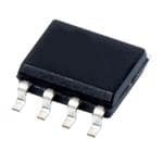
| 产品图片 |
|
| 产品型号 | TLV5638QDRG4 |
| rohs | 无铅 / 符合限制有害物质指令(RoHS)规范要求 |
| 产品系列 | - |
| 产品培训模块 | http://www.digikey.cn/PTM/IndividualPTM.page?site=cn&lang=zhs&ptm=13240 |
| 位数 | 12 |
| 供应商器件封装 | 8-SOIC |
| 其它名称 | 296-29421-6 |
| 制造商产品页 | http://www.ti.com/general/docs/suppproductinfo.tsp?distId=10&orderablePartNumber=TLV5638QDRG4 |
| 包装 | Digi-Reel® |
| 安装类型 | 表面贴装 |
| 封装/外壳 | 8-SOIC(0.154",3.90mm 宽) |
| 工作温度 | -40°C ~ 125°C |
| 建立时间 | 3.5µs |
| 数据接口 | MICROWIRE™,QSPI™,串行,SPI™ |
| 标准包装 | 1 |
| 电压源 | 单电源 |
| 转换器数 | 2 |
| 输出数和类型 | 2 电压,单极 |
| 采样率(每秒) | - |


- 商务部:美国ITC正式对集成电路等产品启动337调查
- 曝三星4nm工艺存在良率问题 高通将骁龙8 Gen1或转产台积电
- 太阳诱电将投资9.5亿元在常州建新厂生产MLCC 预计2023年完工
- 英特尔发布欧洲新工厂建设计划 深化IDM 2.0 战略
- 台积电先进制程称霸业界 有大客户加持明年业绩稳了
- 达到5530亿美元!SIA预计今年全球半导体销售额将创下新高
- 英特尔拟将自动驾驶子公司Mobileye上市 估值或超500亿美元
- 三星加码芯片和SET,合并消费电子和移动部门,撤换高东真等 CEO
- 三星电子宣布重大人事变动 还合并消费电子和移动部门
- 海关总署:前11个月进口集成电路产品价值2.52万亿元 增长14.8%


PDF Datasheet 数据手册内容提取
TLV5638 www.ti.com SLAS225C–JUNE1999–REVISEDJANUARY2004 2.7-V TO 5.5-V LOW-POWER DUAL 12-BIT DIGITAL-TO-ANALOG CONVERTER WITH INTERNAL REFERENCE AND POWER DOWN FEATURES D, JG PACKAGE • Dual12-BitVoltageOutputDAC (TOP VIEW) • ProgrammableInternalReference • ProgrammableSettlingTime: DIN 1 8 VDD SCLK 2 7 OUTB – 1µsinFastMode, CS 3 6 REF – 3.5µsinSlowMode OUTA 4 5 AGND • CompatibleWithTMS320andSPI™Serial Ports • DifferentialNonlinearity<0.5LSBTyp FK PACKAGE • MonotonicOverTemperature (TOP VIEW) D C N C DC APPLICATIONS N DI N V N • DigitalServoControlLoops 3 2 1 20 19 • DigitalOffsetandGainAdjustment NC 4 18 NC • IndustrialProcessControl SCLK 5 17 OUTB • MachineandMotionControlDevices NC 6 16 NC • MassStorageDevices CS 7 15 REF NC 8 14 NC 9 10 11 12 13 C A C D C N T N N N U G O A DESCRIPTION TheTLV5638isadual12-bitvoltageoutputDACwithaflexible3-wireserialinterface. The serial interface allows glueless interface to TMS320, SPI™, QSPI™, and Microwire™ serial ports. It is programmed with a 16-bit serial stringcontaining4controland12databits. The resistor string output voltage is buffered by a x2 gain rail-to-rail output buffer. The buffer features a Class AB output stage to improve stability and reduce settling time. The programmable settling time of the DAC allows the designer to optimize speed vs power dissipation. With its on-chip programmable precision voltage reference, the TLV5638simplifiesoverallsystemdesign. Because of its ability to source up to 1 mA, the reference can also be used as a system reference. Implemented with a CMOS process, the device is designed for single supply operation from 2.7 V to 5.5 V. It is available in an 8-pin SOIC package to reduce board space in standard commercial, industrial, and automotive temperature ranges.ItisalsoavailableinJGandFKpackagesinthemilitarytemperaturerange. Pleasebeawarethatanimportantnoticeconcerningavailability,standardwarranty,anduseincriticalapplicationsofTexas Instrumentssemiconductorproductsanddisclaimerstheretoappearsattheendofthisdatasheet. SPI,QSPIaretrademarksofMotorola,Inc. MicrowireisatrademarkofNationalSemiconductorCorporation. PRODUCTIONDATAinformationiscurrentasofpublicationdate. Copyright©1999–2004,TexasInstrumentsIncorporated Products conform to specifications per the terms of the Texas Instruments standard warranty. Production processing does not necessarilyincludetestingofallparameters.
TLV5638 www.ti.com SLAS225C–JUNE1999–REVISEDJANUARY2004 This integrated circuit can be damaged by ESD. Texas Instruments recommends that all integrated circuits be handled with appropriate precautions. Failure to observe proper handling and installation procedurescancausedamage. ESD damage can range from subtle performance degradation to complete device failure. Precision integrated circuits may be more susceptible to damage because very small parametric changes could causethedevicenottomeetitspublishedspecifications. AVAILABLEOPTIONS PACKAGE TA SOIC CERAMICDIP 20PADLCCC (D) (JG) (FK) 0°Cto70°C TLV5638CD — — 40°Cto85°C TLV5638ID — — TLV5638QD 40°Cto125°C — — TLV5638QDR 55°Cto125°C — TLV5638MJG TLV5638MFK FUNCTIONALBLOCKDIAGRAM REF AGND VDD PGA With Output Enable Voltage Bandgap Power Power-On and Speed Reset Control 2 2 2-Bit Control Latch x2 OUTA DIN 12 12-Bit 12 DAC A Latch SCLK Serial Interface 12 and Buffer CS Control 12 12 12-Bit DAC B Latch x2 OUTB 2
TLV5638 www.ti.com SLAS225C–JUNE1999–REVISEDJANUARY2004 TerminalFunctions TERMINAL I/O/P DESCRIPTION NAME NO. AGND 5 P Ground CS 3 I Chipselect.Digitalinputactivelow,usedtoenable/disableinputs DIN 1 I Digitalserialdatainput OUTA 4 O DACAanalogvoltageoutput OUTB 7 O DACBanalogvoltageoutput REF 6 I/O Analogreferencevoltageinput/output SCLK 2 I Digitalserialclockinput V 8 P Positivepowersupply DD ABSOLUTE MAXIMUM RATINGS overoperatingfree-airtemperaturerange(unlessotherwisenoted)(1) UNIT Supplyvoltage(V toAGND) 7V DD Referenceinputvoltagerange -0.3VtoV +0.3V DD Digitalinputvoltagerange -0.3VtoV +0.3V DD Operatingfree-airtemperaturerange,T TLV5638C 0°Cto70°C A TLV5638I -40°Cto85°C TLV5638Q -40°Cto125°C TLV5638M -55°Cto125°C Storagetemperaturerange,T -65°Cto150°C stg Leadtemperature1,6mm(1/16inch)fromcasefor10seconds 260°C (1) Stressesbeyondthoselistedunder,,absolutemaximumratings”maycausepermanentdamagetothedevice.Thesearestressratings only,andfunctionaloperationofthedeviceattheseoranyotherconditionsbeyondthoseindicatedunder,,recommendedoperating conditions”isnotimplied.Exposuretoabsolute-maximum-ratedconditionsforextendedperiodsmayaffectdevicereliability. DISSIPATION RATING TABLE T £ 25°C DERATINGFACTOR T =70°C T =85°C T =125°C PACKAGE A A A A POWERRATING ABOVET =25°C(1) POWERRATING POWERRATING POWERRATING A D 635mW 5.08mW/°C 407mW 330mW 127mW FK 1375mW 11.00mW/°C 880mW 715mW 275mW JG 1050mW 8.40mW/°C 672mW 546mW 210mW (1) ThisistheinverseofthetraditionalJunction-to-AmbientthermalResistance(Rq ).ThermalResistancesarenotproductiontestedand JA areforinformationalpurposesonly. 3
TLV5638 www.ti.com SLAS225C–JUNE1999–REVISEDJANUARY2004 RECOMMENDED OPERATING CONDITIONS MIN NOM MAX UNIT V =5V 4.5 5 5.5 V DD Supplyvoltage,V DD V =3V 2.7 3 3.3 V DD Poweronreset,POR 0.55(1) 2(1) V V =2.7V 2 V DD High-leveldigitalinputvoltage,V IH V =5.5V 2.4 DD V =2.7V 0.6 V DD Low-leveldigitalinputvoltage,V TLV5638CandTLV5638I 1 IL V =5.5V V DD TLV5638QandTLV5638M 0.8 Referencevoltage,V toREFterminal V =5V (2) AGND 2.048 V -1.5 V ref DD DD Referencevoltage,V toREFterminal V =3V (2) AGND 1.024 V -1.5 V ref DD DD Loadresistance,R 2 kW L Loadcapacitance,C 100 pF L Clockfrequency,f 20 MHz CLK TLV5638C 0 70 TLV5638I 40 85 Operatingfree-airtemperature,T °C A TLV5638Q 40 125 TLV5638M 55 125 (1) ThisparameterisnottestedforQandMsuffixdevices. (2) Duetothex2outputbuffer,areferenceinputvoltage‡ (V -0.4V)/2causesclippingofthetransferfunction.Theoutputbufferofthe DD internalreferencemustbedisabled,ifanexternalreferenceisused. ELECTRICAL CHARACTERISTICS overrecommendedoperatingconditions,V =2.048V,V =1.024V(unlessotherwisenoted) ref ref POWERSUPPLY TLV5638C,I PARAMETER TESTCONDITIONS TLV5638M UNIT MIN TYP MAX V =5V, Fast 4.3 7 DD mA Int.ref. Slow 2.2 3.6 V =3V, Fast 3.8 6.3 DD mA Noload, Int.ref. Slow 1.8 3.0 I Powersupplycurrent Allinputs=AGNDorV , DD DD DAClatch=0x800 V =5V, Fast 3.9 6.3 DD mA Ext.ref. Slow 1.8 3.0 V =3V, Fast 3.5 5.7 DD mA Ext.ref. Slow 1.5 2.6 Power-downsupplycurrent 0.01 10 µA Zeroscale, (1) 65 PSRR Powersupplyrejectionratio dB Fullscale, (2) 65 (1) PowersupplyrejectionratioatzeroscaleismeasuredbyvaryingV andisgivenby:PSRR=20log[(E (V max)- DD ZS DD E (V min))/V max] ZS DD DD (2) PowersupplyrejectionratioatfullscaleismeasuredbyvaryingV andisgivenby:PSRR=20log[(E (V max)- DD G DD E (V min))/V max] G DD DD 4
TLV5638 www.ti.com SLAS225C–JUNE1999–REVISEDJANUARY2004 ELECTRICAL CHARACTERISTICS (Continued) overrecommendedoperatingconditions,V =2.048V,V =1.024V(unlessotherwisenoted) ref ref STATICDACSPECIFICATIONS PARAMETER TESTCONDITIONS MIN TYP MAX UNIT Resolution 12 bits CandI ±1.7 ±4 LSB Integralnonlinearity,endpointad- suffixes INL See (1) justed QandM ±1.7 ±6 LSB suffixes DNL Differentialnonlinearity See (2) ±0.4 ±1 LSB Zero-scaleerror(offseterroratzero E See (3) ±24 mV ZS scale) Zero-scale-errortemperaturecoef- E TC See (4) 10 ppm/°C ZS ficient %full E Gainerror See(5) ±0.6 G scaleV E T Gainerrortemperaturecoefficient See (6) 10 ppm/°C G C OUTPUTSPECIFICATIONS V Outputvoltage R =10kW 0 V -0.4 V O L DD Outputloadregulationaccuracy V =4.096V,2.048V,R =2kW ±0.25 %full O L scaleV REFERENCEPINCONFIGUREDASOUTPUT(REF) Vref(OUTL) Lowreferencevoltage 1.003 1.024 1.045 V Vref(OUTH) Highreferencevoltage V >4.75V 2.027 2.048 2.069 V DD Iref(source) Outputsourcecurrent 1 mA Iref(sink) Outputsinkcurrent -1 mA Loadcapacitance 100 pF PSRR Powersupplyrejectionratio -65 dB REFERENCEPINCONFIGUREDASINPUT(REF) V Inputvoltage 0 V -1.5 V I DD R Inputresistance 10 MW I C Inputcapacitance 5 pF I Fast 1.3 MHz Referenceinputbandwidth REF=0.2V +1.024Vdc pp Slow 525 kHz Referencefeedthrough REF=1V at1.024Vdc(7) -80 dB pp DIGITALINPUTS I HIgh-leveldigitalinputcurrent V =V 1 µA IH I DD I Low-leveldigitalinputcurrent V =0V -1 µA IL I C Inputcapacitance 8 pF i (1) Therelativeaccuracyorintegralnonlinearity(INL)sometimesreferredtoaslinearityerror,isthemaximumdeviationoftheoutputfrom thelinebetweenzeroandfullscaleexcludingtheeffectsofzerocodeandfull-scaleerrors.Testedfromcode32to4095. (2) Thedifferentialnonlinearity(DNL)sometimesreferredtoasdifferentialerror,isthedifferencebetweenthemeasuredandideal1LSB amplitudechangeofanytwoadjacentcodes.Monotonicmeanstheoutputvoltagechangesinthesamedirection(orremainsconstant) asachangeinthedigitalinputcode. (3) Zero-scaleerroristhedeviationfromzerovoltageoutputwhenthedigitalinputcodeiszero. (4) Zero-scale-errortemperaturecoefficientisgivenby:E TC=[E (T )-E (T )]/V ×106/(T -T ). ZS ZS max ZS min ref max min (5) Gainerroristhedeviationfromtheidealoutput(2V -1LSB)withanoutputloadof10kW excludingtheeffectsofthezero-error. ref (6) Gaintemperaturecoefficientisgivenby:E TC=[E (T )-E (T )]/V ×106/(T -T ). G G max G min ref max min (7) ReferencefeedthroughismeasuredattheDACoutputwithaninputcode=0x000. 5
TLV5638 www.ti.com SLAS225C–JUNE1999–REVISEDJANUARY2004 ELECTRICAL CHARACTERISTICS (Continued) overrecommendedoperatingconditions,V =2.048V,V =1.024V(unlessotherwisenoted) ref ref ANALOGOUTPUTDYNAMICPERFORMANCE PARAMETER TESTCONDITIONS MIN TYP MAX UNIT Fast 1 3 t Outputsettlingtime,fullscale R =10kW ,C =100pF,See(1) µs s(FS) L L Slow 3.5 7 Fast 0.5 1.5 t Outputsettlingtime,codetocode R =10kW ,C =100pF,See (2) µs s(CC) L L Slow 1 2 Fast 12 SR Slewrate R =10kW ,C =100pF,See (3) V/µs L L Slow 1.8 Glitchenergy DIN=0to1,FCLK=100kHz,CS=V 5 nV-s DD SNR Signal-to-noiseratio 69 74 S/(N+D) Signal-to-noise+distortion f =480kSPS,f =1kHz,R =10kW , 58 67 s out L dB THD Totalharmonicdistortion CL=100pF 69 57 Spuriousfreedynamicrange 57 72 (1) Settlingtimeisthetimefortheoutputsignaltoremainwithin±0.5LSBofthefinalmeasuredvalueforadigitalinputcodechangeof 0x020to0xFDFand0xFDFto0x020respectively.Nottested,assuredbydesign. (2) Settlingtimeisthetimefortheoutputsignaltoremainwithin±0.5LSBofthefinalmeasuredvalueforadigitalinputcodechangeof onecount.Nottested,assuredbydesign. (3) SlewratedeterminesthetimeittakesforachangeoftheDACoutputfrom10%to90%full-scalevoltage. DIGITAL INPUT TIMING REQUIREMENTS MIN NOM MAX UNIT t Setuptime,CSlowbeforefirstnegativeSCLKedge 10 ns su(CS-CK) t Setuptime,16thnegativeSCLKedge(whenD0issampled)beforeCSrisingedge 10 ns su(C16-CS) t SCLKpulsewidthhigh 25 ns wH t SCLKpulsewidthlow 25 ns wL t Setuptime,datareadybeforeSCLKfallingedge 10 ns su(D) t Holdtime,dataheldvalidafterSCLKfallingedge 5 ns h(D) PARAMETER MEASURMENT INFORMATION twL twH SCLK X 1 2 3 4 5 15 16 X tsu(D) th(D) DIN X D15 D14 D13 D12 D1 D0 X tsu(C16-CS) tsu(CS-CK) CS Figure1.TimingDiagram 6
TLV5638 www.ti.com SLAS225C–JUNE1999–REVISEDJANUARY2004 TYPICAL CHARACTERISTICS POWER DOWN SUPPLY CURRENT SUPPLY CURRENT vs vs TIME FREE-AIR TEMPERATURE 2.6 4.5 2.4 A 4 m 2.2 ent – 2 – mA 3.5 Fast Mode y Curr 11..86 urrent 3 pl C p 1.4 y n Su 1.2 uppl 2.5 w S Do 1 – 2 wer 0.8 IDD Slow Mode Po 0.6 1.5 – D 0.4 VDD = 5 V ID 1 Vref = Int. 2 V 0.2 Input Code = Full Scale (Both DACs) 0 0.5 0 10 20 30 40 50 60 70 80 –40–30–20–10 0 10 20 30 40 50 60 70 80 90 t – Time – m s TA – Free-Air Temperature – °C Figure2. Figure3. SUPPLY CURRENT OUTPUT VOLTAGE vs vs FREE-AIR TEMPERATURE LOAD CURRENT 4.5 2.064 VDD = 3 V VDD = 3 V 4 Vref = Int. 1 V Fast Mode Vref = Int. 1 V Input Code = Full Scale (Both DACs) 2.062 Input Code = 4095 A m – 3.5 y Current 3 Fast Mode oltage – V 2.20.5086 Slow Mode – Suppl 2.52 Output V 2.056 DD Slow Mode – I O2.054 1.5 V 2.052 1 0.5 2.05 –40–30–20–10 0 10 20 30 40 50 60 70 80 90 0 0.5 1 1.5 2 2.5 3 3.5 4 TA – Free-Air Temperature – °C Source Current – mA Figure4. Figure5. 7
TLV5638 www.ti.com SLAS225C–JUNE1999–REVISEDJANUARY2004 TYPICAL CHARACTERISTICS (continued) OUTPUT VOLTAGE OUTPUT VOLTAGE vs vs LOAD CURRENT LOAD CURRENT 4.128 3 VDD = 5 V VDD = 3 V Fast Mode Vref = Int. 2 V Vref = Int. 1 V 4.126 Input Code = 4095 2.5 Input Code = 0 V 4.124 V Fast Mode – – 2 e e g Slow Mode g a a olt 4.122 olt ut V ut V 1.5 p p ut 4.12 ut O O – – 1 O4.118 O V V 0.5 4.116 Slow Mode 4.114 0 0 0.5 1 1.5 2 2.5 3 3.5 4 0 0.5 1 1.5 2 2.5 3 3.5 4 Source Current – mA Sink Current – mA Figure6. Figure7. OUTPUT VOLTAGE TOTAL HARMONIC DISTORTION AND NOISE vs vs LOAD CURRENT FREQUENCY 5 B 0 VDD = 5 V – d VDD = 5 V 4.5 Vref = Int. 2 V e –10 Vref = 1 V dc + 1 V p/p Sinewave Input Code = 0 ois Output Full Scale 4 N –20 d – V 3.5 n an –30 e Fast Mode o oltag 3 storti –40 ut V 2.5 c Di –50 Outp 2 moni –60 – ar Slow Mode O 1.5 H –70 V al 1 Tot –80 Fast Mode – N 0.5 + –90 Slow Mode D H 0 T –100 0 0.5 1 1.5 2 2.5 3 3.5 4 100 1000 10000 100000 Sink Current – mA f – Frequency – Hz Figure8. Figure9. 8
TLV5638 www.ti.com SLAS225C–JUNE1999–REVISEDJANUARY2004 TYPICAL CHARACTERISTICS (continued) TOTAL HARMONIC DISTORTION vs FREQUENCY 0 VDD = 5 V –10 Vref = 1 V dc + 1 V p/p Sinewave B Output Full Scale d – –20 n o rti –30 o st Di –40 c oni –50 m r Ha –60 al ot –70 Slow Mode T – D –80 H T Fast Mode –90 –100 100 1000 10000 100000 f – Frequency – Hz Figure10. INTEGRAL NONLINEARITY ERROR B S 4 L – r 3 o r Er 2 y rit 1 a e n 0 nli No –1 ral –2 g e nt –3 L – I –4 N 0 1024 2048 3072 4096 I Digital Code Figure11. DIFFERENTIAL NONLINEARITY ERROR B S L 1 r – 0.8 o r 0.6 r E y 0.4 aril 0.2 e nlin 0 o –0.2 N al –0.4 nti –0.6 e r e –0.8 Diff –1 – 0 1024 2048 3072 4096 L N Digital Code D Figure12. 9
TLV5638 www.ti.com SLAS225C–JUNE1999–REVISEDJANUARY2004 APPLICATION INFORMATION GENERAL FUNCTION The TLV5638 is a dual 12-bit, single supply DAC, based on a resistor string architecture. It consists of a serial interface, a speed and power-down control logic, a programmable internal reference, a resistor string, and a rail-to-railoutputbuffer. Theoutputvoltage(fullscaledeterminedbyreference)isgivenby: CODE 2REF [V] 0x1000 Where REF is the reference voltage and CODE is the digital input value in the range 0x000 to 0xFFF. A power onresetinitiallyputstheinternallatchestoadefinedstate(allbitszero). SERIAL INTERFACE A falling edge of CS starts shifting the data bit-per-bit (starting with the MSB) to the internal register on the falling edges of SCLK. After 16 bits have been transferred or CS rises, the content of the shift register is moved to the targetlatches(DACA,DACB,BUFFER,CONTROL),dependingonthecontrolbitswithinthedataword. Figure13showsexamplesofhowtoconnecttheTLV5638toTMS320,SPI™,andMicrowire™. TMS320 TLV5638 SPI TLV5638 Microwire TLV5638 DSP FSX CS I/O CS I/O CS DX DIN MOSI DIN SO DIN CLKX SCLK SCK SCLK SK SCLK Figure13.Three-WireInterface Notes on SPI™ and Microwire™: Before the controller starts the data transfer, the software has to generate a falling edge on the pin connected to CS. If the word width is 8 bits (SPI™ and Microwire™), two write operations must be performed to program the TLV5638. After the write operation(s), the holding registers or the control registerareupdatedautomaticallyonthe16thpositiveclockedge. SERIAL CLOCK FREQUENCY AND UPDATE RATE Themaximumserialclockfrequencyisgivenby: f (cid:2) 1 (cid:2)20MHz sclkmax t (cid:1)t whmin wlmin Themaximumupdaterateis: 1 fupdatemax(cid:2) (cid:2)1.25MHz 16(cid:3)twhmin(cid:1)twlmin(cid:4) Note, that the maximum update rate is just a theoretical value for the serial interface, as the settling time of the TLV5638hastobeconsidered,too. 10
TLV5638 www.ti.com SLAS225C–JUNE1999–REVISEDJANUARY2004 APPLICATION INFORMATION (continued) DATA FORMAT The16-bitdatawordfortheTLV5638consistsoftwoparts: • Programbits(D15..D12) • Newdata(D11..D0) D15 D14 D13 D12 D11 D10 D9 D8 D7 D6 D5 D4 D3 D2 D1 D0 R1 SPD PWR R0 12Databits SPD:Speedcontrolbit 1fi fastmode 0fi slowmode PWR:Powercontrolbit 1fi powerdown 0fi normaloperation Thefollowingtableliststhepossiblecombinationoftheregisterselectbits: REGISTERED SELECT BITS R1 R0 REGISTER 0 0 WritedatatoDACBandBUFFER 0 1 WritedatatoBUFFER 1 0 WritedatatoDACAandupdateDACBwithBUFFERcontent 1 1 Writedatatocontrolregister The meaning of the 12 data bits depends on the register. If one of the DAC registers or the BUFFER is selected, thenthe12databitsdeterminethenewDACvalue: DATA BITS: DAC A, DAC B and BUFFER D11 D10 D9 D8 D7 D6 D5 D4 D3 D2 D1 D0 NewDACValue Ifcontrolisselected,thenD1,D0ofthe12databitsareusedtoprogramthereferencevoltage: DATA BITS: CONTROL D11 D10 D9 D8 D7 D6 D5 D4 D3 D2 D1 D0 X X X X X X X X X X REF1 REF0 REF1andREF0determinethereferencesourceand,ifinternalreferenceisselected,thereferencevoltage. REFERENCE BITS REF1 REF0 REFERENCE 0 0 External 0 1 1.024V 1 0 2.048V 1 1 External CAUTION: If external reference voltage is applied to the REF pin, external reference MUST beselected. 11
TLV5638 www.ti.com SLAS225C–JUNE1999–REVISEDJANUARY2004 EXAMPLES OF OPERATION: 1. SetDACAoutput,selectfastmode,selectinternalreferenceat2.048V: a. Setreferencevoltageto2.048V(CONTROLregister) D15 D14 D13 D12 D11 D10 D9 D8 D7 D6 D5 D4 D3 D2 D1 D0 1 1 0 1 0 0 0 0 0 0 0 0 0 0 1 0 b. WritenewDACAvalueandupdateDACAoutput: D15 D14 D13 D12 D11 D10 D9 D8 D7 D6 D5 D4 D3 D2 D1 D0 1 1 0 0 NewDACAoutputvalue TheDACAoutputisupdatedontherisingclockedgeafterD0issampled. To output data consecutively using the same DAC configuration, it is not necessary to program the CONTROLregisteragain. 2. SetDACBoutput,selectfastmode,selectexternalreference: a. Selectexternalreference(CONTROLregister): D15 D14 D13 D12 D11 D10 D9 D8 D7 D6 D5 D4 D3 D2 D1 D0 1 1 0 1 0 0 0 0 0 0 0 0 0 0 0 0 b. WritenewDACBvaluetoBUFFERandupdateDACBoutput: D15 D14 D13 D12 D11 D10 D9 D8 D7 D6 D5 D4 D3 D2 D1 D0 0 1 0 0 NewBUFFERcontentandDACBoutputvalue TheDACAoutputisupdatedontherisingclockedgeafterD0issampled. To output data consecutively using the same DAC configuration, it is not necessary to program the CONTROLregisteragain. 3. Set DAC A value, set DAC B value, update both simultaneously, select slow mode, select internal reference at1.024V: a. Setreferencevoltageto1.024V(CONTROLregister) D15 D14 D13 D12 D11 D10 D9 D8 D7 D6 D5 D4 D3 D2 D1 D0 1 0 0 1 0 0 0 0 0 0 0 0 0 0 0 1 b. WritedataforDACBtoBUFFER: D15 D14 D13 D12 D11 D10 D9 D8 D7 D6 D5 D4 D3 D2 D1 D0 0 0 0 1 NewDACBvalue c. WritenewDACAvalueandupdateDACAandBsimultaneously: D15 D14 D13 D12 D11 D10 D9 D8 D7 D6 D5 D4 D3 D2 D1 D0 1 0 0 0 NewDACAvalue BothoutputsareupdatedontherisingclockedgeafterD0fromtheDACAdatawordissampled. To output data consecutively using the same DAC configuration, it is not necessary to program the CONTROLregisteragain. 1. Setpower-downmode: D15 D14 D13 D12 D11 D10 D9 D8 D7 D6 D5 D4 D3 D2 D1 D0 X X 1 X X X X X X X X X X X X X X=Don'tcare 12
TLV5638 www.ti.com SLAS225C–JUNE1999–REVISEDJANUARY2004 LINEARITY, OFFSET, AND GAIN ERROR USING SINGLE ENDED SUPPLIES Whenanamplifierisoperatedfromasingle supply, the voltage offset can still be either positive or negative. With a positive offset, the output voltage changes on the first code change. With a negative offset, the output voltage maynotchangewiththefirstcode,dependingonthemagnitudeoftheoffsetvoltage. The output amplifier attempts to drive the output to a negative voltage. However, because the most negative supplyrailisground,theoutputcannotdrivebelowgroundandclampstheoutputat0V. The output voltage then remains at zero until the input code value produces a sufficient positive output voltage to overcomethenegativeoffsetvoltage,resultinginthetransferfunctionshowninFigure14. Output Voltage 0 V DAC Code Negative Offset Figure14.EffectofNegativeOffset(SingleSupply) This offset error, not the linearity error, produces this breakpoint. The transfer function would have followed the dottedlineiftheoutputbuffercoulddrivebelowthegroundrail. For a DAC, linearity is measured between zero-input code (all inputs 0) and full-scale code (all inputs 1) after offset and full scale are adjusted out or accounted for in some way. However, single supply operation does not allow for adjustment when the offset is negative due to the breakpoint in the transfer function. So the linearity is measuredbetweenfull-scalecodeandthelowestcodethatproducesapositiveoutputvoltage. 13
TLV5638 www.ti.com SLAS225C–JUNE1999–REVISEDJANUARY2004 DEFINITIONS OF SPECIFICATIONS AND TERMINOLOGY IntegralNonlinearity(INL) The relative accuracy or integral nonlinearity (INL), sometimes referred to as linearity error, is the maximum deviation of the output from the line between zero and full scale excluding the effects of zero code and full-scale errors. DifferentialNonlinearity(DNL) The differential nonlinearity (DNL), sometimes referred to as differential error, is the difference between the measured and ideal 1 LSB amplitude change of any two adjacent codes. Monotonic means the output voltage changesinthesamedirection(orremainsconstant)asachangeinthedigitalinputcode. Zero-ScaleError(E ) ZS Zero-scaleerrorisdefinedasthedeviationoftheoutputfrom0Vatadigitalinputvalueof0. GainError(E ) G GainerroristheerrorinslopeoftheDACtransferfunction. TotalHarmonicDistortion(THD) THDistheratioofthermsvalueof the first six harmonic components to the value of the fundamental signal. The valueforTHDisexpressedindecibels. Signal-to-NoiseRatio+Distortion(S/N+D) S/N+Distheratioofthermsvalueoftheoutputsignaltothermssumofallotherspectral components below the Nyquistfrequency,includingharmonicsbutexcludingdc.ThevalueforS/N+Disexpressedindecibels. SpuriousFreeDynamicRange(SFDR) Spurious free dynamic range is the difference between the rms value of the output signal and the rms value of thelargestspurioussignalwithinaspecifiedbandwidth.ThevalueforSFDRisexpressedindecibels. 14
PACKAGE OPTION ADDENDUM www.ti.com 6-Feb-2020 PACKAGING INFORMATION Orderable Device Status Package Type Package Pins Package Eco Plan Lead/Ball Finish MSL Peak Temp Op Temp (°C) Device Marking Samples (1) Drawing Qty (2) (6) (3) (4/5) 5962-9957601Q2A ACTIVE LCCC FK 20 1 TBD POST-PLATE N / A for Pkg Type -55 to 125 5962- 9957601Q2A TLV5638 MFKB 5962-9957601QPA ACTIVE CDIP JG 8 1 TBD Call TI N / A for Pkg Type -55 to 125 9957601QPA TLV5638M TLV5638CD ACTIVE SOIC D 8 75 Green (RoHS NIPDAU Level-1-260C-UNLIM 0 to 70 5638C & no Sb/Br) TLV5638CDG4 ACTIVE SOIC D 8 75 Green (RoHS NIPDAU Level-1-260C-UNLIM 0 to 70 5638C & no Sb/Br) TLV5638CDR ACTIVE SOIC D 8 2500 Green (RoHS NIPDAU Level-1-260C-UNLIM 0 to 70 5638C & no Sb/Br) TLV5638CDRG4 ACTIVE SOIC D 8 2500 Green (RoHS NIPDAU Level-1-260C-UNLIM 0 to 70 5638C & no Sb/Br) TLV5638ID ACTIVE SOIC D 8 75 Green (RoHS NIPDAU Level-1-260C-UNLIM -40 to 85 5638I & no Sb/Br) TLV5638IDG4 ACTIVE SOIC D 8 75 Green (RoHS NIPDAU Level-1-260C-UNLIM -40 to 85 5638I & no Sb/Br) TLV5638IDR ACTIVE SOIC D 8 2500 Green (RoHS NIPDAU Level-1-260C-UNLIM -40 to 85 5638I & no Sb/Br) TLV5638IDRG4 ACTIVE SOIC D 8 2500 Green (RoHS NIPDAU Level-1-260C-UNLIM -40 to 85 5638I & no Sb/Br) TLV5638MFKB ACTIVE LCCC FK 20 1 TBD POST-PLATE N / A for Pkg Type -55 to 125 5962- 9957601Q2A TLV5638 MFKB TLV5638MJGB ACTIVE CDIP JG 8 1 TBD Call TI N / A for Pkg Type -55 to 125 9957601QPA TLV5638M TLV5638QD ACTIVE SOIC D 8 75 Green (RoHS NIPDAU Level-1-260C-UNLIM -40 to 125 V5638 & no Sb/Br) TLV5638QDG4 ACTIVE SOIC D 8 75 Green (RoHS NIPDAU Level-1-260C-UNLIM V5638 & no Sb/Br) TLV5638QDR ACTIVE SOIC D 8 2500 Green (RoHS NIPDAU Level-1-260C-UNLIM -40 to 125 V5638 & no Sb/Br) Addendum-Page 1
PACKAGE OPTION ADDENDUM www.ti.com 6-Feb-2020 Orderable Device Status Package Type Package Pins Package Eco Plan Lead/Ball Finish MSL Peak Temp Op Temp (°C) Device Marking Samples (1) Drawing Qty (2) (6) (3) (4/5) TLV5638QDRG4 ACTIVE SOIC D 8 2500 Green (RoHS NIPDAU Level-1-260C-UNLIM V5638 & no Sb/Br) (1) The marketing status values are defined as follows: ACTIVE: Product device recommended for new designs. LIFEBUY: TI has announced that the device will be discontinued, and a lifetime-buy period is in effect. NRND: Not recommended for new designs. Device is in production to support existing customers, but TI does not recommend using this part in a new design. PREVIEW: Device has been announced but is not in production. Samples may or may not be available. OBSOLETE: TI has discontinued the production of the device. (2) RoHS: TI defines "RoHS" to mean semiconductor products that are compliant with the current EU RoHS requirements for all 10 RoHS substances, including the requirement that RoHS substance do not exceed 0.1% by weight in homogeneous materials. Where designed to be soldered at high temperatures, "RoHS" products are suitable for use in specified lead-free processes. TI may reference these types of products as "Pb-Free". RoHS Exempt: TI defines "RoHS Exempt" to mean products that contain lead but are compliant with EU RoHS pursuant to a specific EU RoHS exemption. Green: TI defines "Green" to mean the content of Chlorine (Cl) and Bromine (Br) based flame retardants meet JS709B low halogen requirements of <=1000ppm threshold. Antimony trioxide based flame retardants must also meet the <=1000ppm threshold requirement. (3) MSL, Peak Temp. - The Moisture Sensitivity Level rating according to the JEDEC industry standard classifications, and peak solder temperature. (4) There may be additional marking, which relates to the logo, the lot trace code information, or the environmental category on the device. (5) Multiple Device Markings will be inside parentheses. Only one Device Marking contained in parentheses and separated by a "~" will appear on a device. If a line is indented then it is a continuation of the previous line and the two combined represent the entire Device Marking for that device. (6) Lead/Ball Finish - Orderable Devices may have multiple material finish options. Finish options are separated by a vertical ruled line. Lead/Ball Finish values may wrap to two lines if the finish value exceeds the maximum column width. Important Information and Disclaimer:The information provided on this page represents TI's knowledge and belief as of the date that it is provided. TI bases its knowledge and belief on information provided by third parties, and makes no representation or warranty as to the accuracy of such information. Efforts are underway to better integrate information from third parties. TI has taken and continues to take reasonable steps to provide representative and accurate information but may not have conducted destructive testing or chemical analysis on incoming materials and chemicals. TI and TI suppliers consider certain information to be proprietary, and thus CAS numbers and other limited information may not be available for release. In no event shall TI's liability arising out of such information exceed the total purchase price of the TI part(s) at issue in this document sold by TI to Customer on an annual basis. OTHER QUALIFIED VERSIONS OF TLV5638, TLV5638M : •Catalog: TLV5638 Addendum-Page 2
PACKAGE OPTION ADDENDUM www.ti.com 6-Feb-2020 •Enhanced Product: TLV5638-EP, TLV5638-EP •Military: TLV5638M NOTE: Qualified Version Definitions: •Catalog - TI's standard catalog product •Enhanced Product - Supports Defense, Aerospace and Medical Applications •Military - QML certified for Military and Defense Applications Addendum-Page 3
PACKAGE MATERIALS INFORMATION www.ti.com 31-May-2019 TAPE AND REEL INFORMATION *Alldimensionsarenominal Device Package Package Pins SPQ Reel Reel A0 B0 K0 P1 W Pin1 Type Drawing Diameter Width (mm) (mm) (mm) (mm) (mm) Quadrant (mm) W1(mm) TLV5638CDR SOIC D 8 2500 330.0 12.4 6.4 5.2 2.1 8.0 12.0 Q1 TLV5638IDR SOIC D 8 2500 330.0 12.4 6.4 5.2 2.1 8.0 12.0 Q1 TLV5638QDR SOIC D 8 2500 330.0 12.4 6.4 5.2 2.1 8.0 12.0 Q1 PackMaterials-Page1
PACKAGE MATERIALS INFORMATION www.ti.com 31-May-2019 *Alldimensionsarenominal Device PackageType PackageDrawing Pins SPQ Length(mm) Width(mm) Height(mm) TLV5638CDR SOIC D 8 2500 350.0 350.0 43.0 TLV5638IDR SOIC D 8 2500 367.0 367.0 35.0 TLV5638QDR SOIC D 8 2500 350.0 350.0 43.0 PackMaterials-Page2
None
PACKAGE OUTLINE D0008A SOIC - 1.75 mm max height SCALE 2.800 SMALL OUTLINE INTEGRATED CIRCUIT C SEATING PLANE .228-.244 TYP [5.80-6.19] .004 [0.1] C A PIN 1 ID AREA 6X .050 [1.27] 8 1 2X .189-.197 [4.81-5.00] .150 NOTE 3 [3.81] 4X (0 -15 ) 4 5 8X .012-.020 B .150-.157 [0.31-0.51] .069 MAX [3.81-3.98] .010 [0.25] C A B [1.75] NOTE 4 .005-.010 TYP [0.13-0.25] 4X (0 -15 ) SEE DETAIL A .010 [0.25] .004-.010 0 - 8 [0.11-0.25] .016-.050 [0.41-1.27] DETAIL A (.041) TYPICAL [1.04] 4214825/C 02/2019 NOTES: 1. Linear dimensions are in inches [millimeters]. Dimensions in parenthesis are for reference only. Controlling dimensions are in inches. Dimensioning and tolerancing per ASME Y14.5M. 2. This drawing is subject to change without notice. 3. This dimension does not include mold flash, protrusions, or gate burrs. Mold flash, protrusions, or gate burrs shall not exceed .006 [0.15] per side. 4. This dimension does not include interlead flash. 5. Reference JEDEC registration MS-012, variation AA. www.ti.com
EXAMPLE BOARD LAYOUT D0008A SOIC - 1.75 mm max height SMALL OUTLINE INTEGRATED CIRCUIT 8X (.061 ) [1.55] SYMM SEE DETAILS 1 8 8X (.024) [0.6] SYMM (R.002 ) TYP [0.05] 5 4 6X (.050 ) [1.27] (.213) [5.4] LAND PATTERN EXAMPLE EXPOSED METAL SHOWN SCALE:8X SOLDER MASK SOLDER MASK METAL OPENING OPENING METAL UNDER SOLDER MASK EXPOSED METAL EXPOSED METAL .0028 MAX .0028 MIN [0.07] [0.07] ALL AROUND ALL AROUND NON SOLDER MASK SOLDER MASK DEFINED DEFINED SOLDER MASK DETAILS 4214825/C 02/2019 NOTES: (continued) 6. Publication IPC-7351 may have alternate designs. 7. Solder mask tolerances between and around signal pads can vary based on board fabrication site. www.ti.com
EXAMPLE STENCIL DESIGN D0008A SOIC - 1.75 mm max height SMALL OUTLINE INTEGRATED CIRCUIT 8X (.061 ) [1.55] SYMM 1 8 8X (.024) [0.6] SYMM (R.002 ) TYP [0.05] 5 4 6X (.050 ) [1.27] (.213) [5.4] SOLDER PASTE EXAMPLE BASED ON .005 INCH [0.125 MM] THICK STENCIL SCALE:8X 4214825/C 02/2019 NOTES: (continued) 8. Laser cutting apertures with trapezoidal walls and rounded corners may offer better paste release. IPC-7525 may have alternate design recommendations. 9. Board assembly site may have different recommendations for stencil design. www.ti.com
MECHANICAL DATA MCER001A – JANUARY 1995 – REVISED JANUARY 1997 JG (R-GDIP-T8) CERAMIC DUAL-IN-LINE 0.400 (10,16) 0.355 (9,00) 8 5 0.280 (7,11) 0.245 (6,22) 1 4 0.065 (1,65) 0.045 (1,14) 0.063 (1,60) 0.020 (0,51) MIN 0.310 (7,87) 0.015 (0,38) 0.290 (7,37) 0.200 (5,08) MAX Seating Plane 0.130 (3,30) MIN 0.023 (0,58) 0°–15° 0.015 (0,38) 0.100 (2,54) 0.014 (0,36) 0.008 (0,20) 4040107/C 08/96 NOTES: A. All linear dimensions are in inches (millimeters). B. This drawing is subject to change without notice. C. This package can be hermetically sealed with a ceramic lid using glass frit. D. Index point is provided on cap for terminal identification. E. Falls within MIL STD 1835 GDIP1-T8 • POST OFFICE BOX 655303 DALLAS, TEXAS 75265
IMPORTANTNOTICEANDDISCLAIMER TI PROVIDES TECHNICAL AND RELIABILITY DATA (INCLUDING DATASHEETS), DESIGN RESOURCES (INCLUDING REFERENCE DESIGNS), APPLICATION OR OTHER DESIGN ADVICE, WEB TOOLS, SAFETY INFORMATION, AND OTHER RESOURCES “AS IS” AND WITH ALL FAULTS, AND DISCLAIMS ALL WARRANTIES, EXPRESS AND IMPLIED, INCLUDING WITHOUT LIMITATION ANY IMPLIED WARRANTIES OF MERCHANTABILITY, FITNESS FOR A PARTICULAR PURPOSE OR NON-INFRINGEMENT OF THIRD PARTY INTELLECTUAL PROPERTY RIGHTS. These resources are intended for skilled developers designing with TI products. You are solely responsible for (1) selecting the appropriate TI products for your application, (2) designing, validating and testing your application, and (3) ensuring your application meets applicable standards, and any other safety, security, or other requirements. These resources are subject to change without notice. TI grants you permission to use these resources only for development of an application that uses the TI products described in the resource. Other reproduction and display of these resources is prohibited. No license is granted to any other TI intellectual property right or to any third party intellectual property right. TI disclaims responsibility for, and you will fully indemnify TI and its representatives against, any claims, damages, costs, losses, and liabilities arising out of your use of these resources. TI’s products are provided subject to TI’s Terms of Sale (www.ti.com/legal/termsofsale.html) or other applicable terms available either on ti.com or provided in conjunction with such TI products. TI’s provision of these resources does not expand or otherwise alter TI’s applicable warranties or warranty disclaimers for TI products. Mailing Address: Texas Instruments, Post Office Box 655303, Dallas, Texas 75265 Copyright © 2020, Texas Instruments Incorporated