ICGOO在线商城 > 集成电路(IC) > 数据采集 - 数模转换器 > AD5530BRUZ
 Datasheet下载
- 型号: AD5530BRUZ
- 制造商: Analog
- 库位|库存: xxxx|xxxx
- 要求:
| 数量阶梯 | 香港交货 | 国内含税 |
| +xxxx | $xxxx | ¥xxxx |
查看当月历史价格
查看今年历史价格
AD5530BRUZ产品简介:
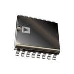
ICGOO电子元器件商城为您提供AD5530BRUZ由Analog设计生产,在icgoo商城现货销售,并且可以通过原厂、代理商等渠道进行代购。 AD5530BRUZ价格参考。AnalogAD5530BRUZ封装/规格:数据采集 - 数模转换器, 12 位 数模转换器 1 16-TSSOP。您可以下载AD5530BRUZ参考资料、Datasheet数据手册功能说明书,资料中有AD5530BRUZ 详细功能的应用电路图电压和使用方法及教程。
AD5530BRUZ 是由 Analog Devices Inc.(亚德诺半导体)生产的一款高性能数模转换器(DAC),属于数据采集 - 数模转换器类别。其应用场景广泛,主要集中在需要高精度、低噪声和高速性能的领域。以下是该型号的主要应用场景:

1. 工业自动化与控制
   AD5530BRUZ 可用于工业自动化中的精密控制任务,例如伺服电机控制、机器人运动控制以及过程控制系统。其高分辨率和低噪声特性使其能够精确地生成模拟信号以驱动执行器或调节设备。

2. 测试与测量设备
   在高端测试仪器中,如信号发生器、数字万用表和示波器校准设备,AD5530BRUZ 提供了高精度的输出能力,确保测试结果的准确性和可靠性。

3. 通信系统
   该器件适用于无线通信基站、软件定义无线电(SDR)和其他通信设备中的信号生成模块。它能够产生高质量的射频或中频信号,支持复杂的调制方案。

4. 医疗设备
   在医疗成像设备(如超声波、CT 和 MRI)以及患者监护仪中,AD5530BRUZ 的高精度特性可用于生成稳定的激励信号或控制信号,从而提高诊断和监测的准确性。

5. 音频处理
   对于专业音频设备,如数字混音台、音频接口和高保真音响系统,AD5530BRUZ 能够提供纯净的音频信号输出,满足对音质要求极高的应用需求。

6. 航空航天与国防
   在雷达系统、导航设备和卫星通信中,AD5530BRUZ 的稳定性和可靠性使其成为理想选择,用于生成精确的控制信号或模拟复杂的工作环境。

总结来说,AD5530BRUZ 凭借其卓越的性能参数,特别适合需要高精度、低失真和宽动态范围的应用场景,覆盖工业、通信、医疗、音频及国防等多个领域。
| 参数 | 数值 |
| 产品目录 | 集成电路 (IC)半导体 |
| 描述 | IC DAC 12BIT SRL IN/VOUT 16TSSOP数模转换器- DAC 12-BIT VTG OUTPUT IC |
| 产品分类 | |
| 品牌 | Analog Devices |
| 产品手册 | |
| 产品图片 |
|
| rohs | 符合RoHS无铅 / 符合限制有害物质指令(RoHS)规范要求 |
| 产品系列 | 数据转换器IC,数模转换器- DAC,Analog Devices AD5530BRUZ- |
| 数据手册 | |
| 产品型号 | AD5530BRUZ |
| 产品培训模块 | http://www.digikey.cn/PTM/IndividualPTM.page?site=cn&lang=zhs&ptm=19145http://www.digikey.cn/PTM/IndividualPTM.page?site=cn&lang=zhs&ptm=18614http://www.digikey.cn/PTM/IndividualPTM.page?site=cn&lang=zhs&ptm=26125http://www.digikey.cn/PTM/IndividualPTM.page?site=cn&lang=zhs&ptm=26140http://www.digikey.cn/PTM/IndividualPTM.page?site=cn&lang=zhs&ptm=26150http://www.digikey.cn/PTM/IndividualPTM.page?site=cn&lang=zhs&ptm=26147 |
| 产品目录页面 | |
| 产品种类 | 数模转换器- DAC |
| 位数 | 12 |
| 供应商器件封装 | 16-TSSOP |
| 分辨率 | 12 bit |
| 包装 | 管件 |
| 商标 | Analog Devices |
| 安装类型 | 表面贴装 |
| 安装风格 | SMD/SMT |
| 封装 | Tube |
| 封装/外壳 | 16-TSSOP(0.173",4.40mm 宽) |
| 封装/箱体 | TSSOP-16 |
| 工作温度 | -40°C ~ 85°C |
| 工厂包装数量 | 96 |
| 建立时间 | 20µs |
| 接口类型 | SPI |
| 数据接口 | 串行 |
| 最大功率耗散 | 60 mW |
| 最大工作温度 | + 85 C |
| 最小工作温度 | - 40 C |
| 标准包装 | 96 |
| 电压参考 | External |
| 电压源 | 模拟和数字 |
| 电源电压-最大 | 16.5 V |
| 电源电压-最小 | 10.8 V |
| 积分非线性 | +/- 1 LSB |
| 稳定时间 | 20 us |
| 系列 | AD5530 |
| 结构 | R-2R |
| 转换器数 | 1 |
| 转换器数量 | 1 |
| 输出数和类型 | 1 电压,双极 |
| 输出类型 | Voltage |
| 采样比 | 50 kSPs |
| 采样率(每秒) | 50k |


- 商务部:美国ITC正式对集成电路等产品启动337调查
- 曝三星4nm工艺存在良率问题 高通将骁龙8 Gen1或转产台积电
- 太阳诱电将投资9.5亿元在常州建新厂生产MLCC 预计2023年完工
- 英特尔发布欧洲新工厂建设计划 深化IDM 2.0 战略
- 台积电先进制程称霸业界 有大客户加持明年业绩稳了
- 达到5530亿美元!SIA预计今年全球半导体销售额将创下新高
- 英特尔拟将自动驾驶子公司Mobileye上市 估值或超500亿美元
- 三星加码芯片和SET,合并消费电子和移动部门,撤换高东真等 CEO
- 三星电子宣布重大人事变动 还合并消费电子和移动部门
- 海关总署:前11个月进口集成电路产品价值2.52万亿元 增长14.8%


PDF Datasheet 数据手册内容提取
Serial Input, Voltage Output 12-/14-Bit Digital-to-Analog Converters AD5530/AD5531 FEATURES FUNCTIONAL BLOCK DIAGRAM Pin-compatible 12-, 14-bit digital-to-analog converters VSS VDD Serial input, voltage output AD5530/AD5531 REFIN Maximum output voltage range of ±10 V Data readback R R 12-D/1A4C-BIT VOUT 3-wire serial interface REFAGND R Clear function to a user-defined voltage R LDAC Power-down function DAC REGISTER DUTGND RBEN CLR Serial data output for daisy-chaining 16-lead TSSOP SDIN SHIFT REGISTER CPOONWTREORL-D LOOWGNIC PD APPLICATIONS GND SCLK SYNC SDO 00938-001 Industrial automation Figure 1. Automatic test equipment Process control General-purpose instrumentation GENERAL DESCRIPTION The AD5530/AD5531 are single 12- and 14-bit (respectively) The DAC output is buffered by a gain of two amplifier and serial input, voltage output digital-to-analog converters (DAC). referenced to the potential at DUTGND. LDAC can be used to update the output of the DAC asynchronously. A power-down They utilize a versatile 3-wire interface that is compatible with SPI®, QSPI™, MICROWIRE™, and DSP interface standards. Data pin (PD) allows the DAC to be put into a low power state, and is presented to the part in a 16-bit serial word format. Serial a CLR pin allows the output to be cleared to a user-defined data is available on the SDO pin for daisy-chaining purposes. voltage, the potential at DUTGND. Data readback allows the user to read the contents of the DAC The AD5530/AD5531 are available in 16-lead TSSOP. register via the SDO pin. Rev. B Information furnished by Analog Devices is believed to be accurate and reliable. However, no responsibility is assumed by Analog Devices for its use, nor for any infringements of patents or other One Technology Way, P.O. Box 9106, Norwood, MA 02062-9106, U.S.A. rights of third parties that may result from its use. Specifications subject to change without notice. No license is granted by implication or otherwise under any patent or patent rights of Analog Devices. Tel: 781.329.4700 www.analog.com Trademarks and registered trademarks are the property of their respective owners. Fax: 781.461.3113 ©2007 Analog Devices, Inc. All rights reserved.
AD5530/AD5531 TABLE OF CONTENTS Features..............................................................................................1 PD Function................................................................................13 Applications.......................................................................................1 Readback Function....................................................................13 Functional Block Diagram..............................................................1 CLR Function..............................................................................13 General Description.........................................................................1 Output Voltage............................................................................14 Revision History...............................................................................2 Bipolar Configuration................................................................14 Specifications.....................................................................................3 Microprocessor Interfacing...........................................................15 AC Performance Characteristics................................................5 AD5530/AD5531 to ADSP-21xx..............................................15 Standalone Timing Characteristics............................................5 AD5530/AD5531 to 8051 Interface.........................................15 Daisy-Chaining and Readback Timing Characteristics..........6 AD5530/AD5531 to MC68HC11 Interface............................15 Absolute Maximum Ratings............................................................7 Applications Information..............................................................17 ESD Caution..................................................................................7 Optocoupler Interface................................................................17 Pin Configuration and Function Descriptions.............................8 Serial Interface to Multiple AD5530s or AD5531s................17 Typical Performance Characteristics.............................................9 Daisy-Chaining Interface with Multiple AD5530s or Terminology....................................................................................12 AD5531s......................................................................................17 Theory of Operation......................................................................13 Outline Dimensions.......................................................................18 DAC Architecture.......................................................................13 Ordering Guide..........................................................................18 Serial Interface............................................................................13 REVISION HISTORY 1/07—Rev. A to Rev. B Updated Format..................................................................Universal Changes to Figure 28......................................................................17 3/06—Rev. 0 to Rev. A Change to Table 3.............................................................................5 Change to Figure 4...........................................................................8 Change to Output Voltage Section...............................................14 Change to Ordering Guide............................................................18 5/02—Revision 0: Initial Version Rev. B | Page 2 of 20
AD5530/AD5531 SPECIFICATIONS V = 15 V ± 10%; V = −15 V ± 10%; GND = 0 V; R = 5 kΩ and C = 220 pF to GND. All specifications T to T , unless otherwise noted. DD SS L L MIN MAX Table 1. Parameter1 AD5530 AD5531 Unit Test Conditions/Comments ACCURACY Resolution 12 14 Bits Relative Accuracy ±1 ±2 LSB max Differential Nonlinearity ±1 ±1 LSB max Guaranteed monotonic over temperature Zero-Scale Error ±2 ±8 LSB max Typically within ±1 LSB Full-Scale Error ±2 ±8 LSB max Typically within ±1 LSB Gain Error ±1 ±4 LSB typ Gain Temperature Coefficient2 0.5 0.5 ppm FSR/°C typ 10 10 ppm FSR/°C max REFERENCE INPUTS2 Reference Input Range 0 to 5 0 to 5 V min to V max Max output range ±10 V DC Input Resistance 100 100 MΩ typ Input Current ±1 ±1 μA max Per input, typically ±20 nA DUTGND INPUT2 DC Input Impedance 60 60 kΩ typ Max Input Current ±0.3 ±0.3 mA typ Input Range −4 to +4 −4 to +4 V min to V max Max output range ±10 V O/P CHARACTERISTICS2 Output Voltage Swing ±10 ±10 V max Short-Circuit Current 15 15 mA max Resistive Load 5 5 kΩ min To 0 V Capacitive Load 1200 1200 pF max To 0 V DC Output Impedance 0.5 0.5 Ω max DIGITAL I/O V , Input High Voltage 2.4 2.4 V min INH V , Input Low Voltage 0.8 0.8 V max INL I , Input Current ±10 ±10 μA max Total for all pins INH C , Input Capacitance2 10 10 pF max 3 pF typical IN SDO V , Output Low Voltage 0.4 0.4 V max I = 1 mA OL SINK POWER REQUIREMENTS V /V +15/−15 +15/−15 V nom ±10% for specified performance DD SS Power Supply Sensitivity ΔFull Scale/ΔV 110 110 dB typ DD ΔFull Scale/ΔV 100 100 dB typ SS I 2 2 mA max Outputs unloaded DD I 2 2 mA max Outputs unloaded SS I in Power-Down 150 150 μA max Typically 50 μA DD 1 Temperature range for B Version: −40°C to +85°C. 2 Guaranteed by design, not subject to production test. Rev. B | Page 3 of 20
AD5530/AD5531 V = 12 V ± 10%; V = −12 V ± 10%; GND = 0 V; R = 5 kΩ and C = 220 pF to GND; T = T to T , unless otherwise noted. DD SS L L A MIN MAX Table 2. Parameter1 AD5530 AD5531 Unit Test Conditions/Comments ACCURACY Resolution 12 14 Bits Relative Accuracy ±1 ±2 LSB max Differential Nonlinearity ±1 ±1 LSB max Guaranteed monotonic over temperature Zero-Scale Error ±2 ±8 LSB max Typically within ±1 LSB Full-Scale Error ±2 ±8 LSB max Typically within ±1 LSB Gain Error ±1 ±4 LSB typ Gain Temperature Coefficient2 0.5 0.5 ppm FSR/°C typ 10 10 ppm FSR/°C max REFERENCE INPUTS2 Reference Input Range 0 to 4.096 0 to 4.096 V min to V max Max output range ±8.192 V DC Input Resistance 100 100 MΩ typ Input Current ±1 ±1 μA max Per input, typically ±20 nA DUTGND INPUT2 DC Input Impedance 60 60 kΩ typ Max Input Current ±0.3 ±0.3 mA typ Input Range −3 to +3 −3 to +3 V min to V max Max output range ±8.192 V O/P CHARACTERISTICS2 Output Voltage Swing ±8.192 ±8.192 V max Short-Circuit Current 15 15 mA max Resistive Load 5 5 kΩ min To 0 V Capacitive Load 1200 1200 pF max To 0 V DC Output Impedance 0.5 0.5 Ω max DIGITAL I/O V , Input High Voltage 2.4 2.4 V min INH V , Input Low Voltage 0.8 0.8 V max INL I , Input Current ±10 ±10 μA max Total for all pins INH C , Input Capacitance2 10 10 pF max 3 pF typical IN SDO V , Output Low Voltage 0.4 0.4 V max I = 1 mA OL SINK POWER REQUIREMENTS V /V +12/−12 +12/−12 V nom ±10% for specified performance DD SS Power Supply Sensitivity ΔFull Scale/ΔV 110 110 dB typ DD ΔFull Scale/ΔV 100 100 dB typ SS I 2 2 mA max Outputs unloaded DD I 2 2 mA max Outputs unloaded SS I in Power-Down 150 150 μA max Typically 50 μA DD 1 Temperature range for B Version: −40°C to +85°C. 2 Guaranteed by design, not subject to production test. Rev. B | Page 4 of 20
AD5530/AD5531 AC PERFORMANCE CHARACTERISTICS V = 10.8 V to 16.5 V, V = −10.8 V to −16.5 V; GND = 0 V; R = 5 kΩ and C = 220 pF to GND. All specifications T to T , unless DD SS L L MIN MAX otherwise noted. Table 3. Parameter B Version Unit Test Conditions/Comments DYNAMIC PERFORMANCE Output Voltage Settling Time 20 μs typ Full-scale change to ±½ LSB. DAC latch contents alternately loaded with all 0s and all 1s. Slew Rate 1.3 V/μs typ Digital-to-Analog Glitch Impulse 120 nV-s typ DAC latch alternately loaded with 0x0FFF and 0x1000. Not dependent on load conditions. Digital Feedthrough 0.5 nV-s typ Effect of input bus activity on DAC output under test. Output Noise Spectral Density @ 1 kHz 100 nV/√Hz typ All 1s loaded to DAC. STANDALONE TIMING CHARACTERISTICS V = 10.8 V to 16.5 V, V = −10.8 V to −16.5 V; GND = 0 V; R = 5 kΩ and C = 220 pF to GND. All specifications T to T , unless DD SS L L MIN MAX otherwise noted. Table 4. Parameter1, 2 Limit at T , T Unit Description MIN MAX f 7 MHz max SCLK frequency MAX t 140 ns min SCLK cycle time 1 t 60 ns min SCLK low time 2 t 60 ns min SCLK high time 3 t 50 ns min SYNC to SCLK falling edge setup time 4 t 40 ns min SCLK falling edge to SYNC rising edge 5 t 50 ns min Min SYNC high time 6 t 40 ns min Data setup time 7 t 15 ns min Data hold time 8 t 5 ns min SYNC high to LDAC low 9 t 50 ns min LDAC pulse width 10 t 5 ns min LDAC high to SYNC low 11 t12 50 ns min CLR pulse width 1 Guaranteed by design, not subject to production test. 2 Sample tested during initial release and after any redesign or process change that can affect this parameter. All input signals are measured with tR = tF = 5 ns (10% to 90% of VDD) and timed from a voltage level of (VIL + VIH)/2. t t 1 3 SCLK t4 t t2 5 SYNC t 6 t t 7 8 MSB LSB SDIN DB15 DB14 DB11 DB0 t 9 t 11 LDAC1 t 10 t 12 CLR1LDAC CAN BE TIED PERMANENTLY LOW, IF REQUIRED. 00938-002 Figure 2. Timing Diagram for Standalone Mode Rev. B | Page 5 of 20
AD5530/AD5531 DAISY-CHAINING AND READBACK TIMING CHARACTERISTICS V = 10.8 V to 16.5 V, V = −10.8 V to −16.5 V; GND = 0 V; R = 5 kΩ and C = 220 pF to GND. All specifications T to T , unless DD SS L L MIN MAX otherwise noted. Table 5. Parameter1, 2, 3 Limit at T , T Unit Description MIN MAX f 2 MHz max SCLK frequency MAX t 500 ns min SCLK cycle time 1 t 200 ns min SCLK low time 2 t 200 ns min SCLK high time 3 t 50 ns min SYNC to SCLK falling edge setup time 4 t 40 ns min SCLK falling edge to SYNC rising edge 5 t 50 ns min Min SYNC high time 6 t 40 ns min Data setup time 7 t 15 ns min Data hold time 8 t 50 ns min CLR pulse width 12 t 130 ns min SCLK falling edge to SDO valid 13 t 50 ns max SCLK falling edge to SDO invalid 14 t 50 ns min RBEN to SCLK falling edge setup time 15 t 50 ns min RBEN hold time 16 t 100 ns min RBEN falling edge to SDO valid 17 1 Guaranteed by design, not subject to production test. 2 Sample tested during initial release and after any redesign or process change that can affect this parameter. All input signals are measured with tR = tF = 5 ns (10% to 90% of VDD) and timed from a voltage level of (VIL + VIH)/2. 3 SDO; RPULLUP = 5 kΩ, CL = 15 pF t1 t3 SCLK t4 t5 t2 SYNC t 6 t t MSB 7 8 LSB SDIN DB15 DB14 DB11 DB0 t13 MSB t14 LSB SDO (DAISY- DB15 DB11 DB0 CHAINING) t 15 RBEN t16 t17 t13 t 14 (READBASCDKO) MSB 0 0 RB13 LRSBB0 00938-003 Figure 3. Timing Diagram for Daisy-Chaining and Readback Mode Rev. B | Page 6 of 20
AD5530/AD5531 ABSOLUTE MAXIMUM RATINGS T = 25°C, unless otherwise noted. A Stresses above those listed under Absolute Maximum Ratings may cause permanent damage to the device. This is a stress Table 6. rating only; functional operation of the device at these or any Parameter Rating other conditions above those indicated in the operational V to GND −0.3 V to +17 V DD section of this specification is not implied. Exposure to absolute V to GND +0.3 V to −17 V SS maximum rating conditions for extended periods may affect Digital Inputs to GND −0.3 V to V + 0.3 V DD device reliability. SDO to GND −0.3 V to +6.5 V REFIN to REFAGND −0.3 V to +17 V REFIN to GND VSS − 0.3 V to VDD + 0.3 V ESD CAUTION REFAGND to GND V − 0.3 V to V + 0.3 V SS DD DUTGND to GND V − 0.3 V to V + 0.3 V SS DD Operating Temperature Range Industrial (B Version) −40°C to +85°C Storage Temperature Range −65°C to +150°C Maximum Junction Temperature (T ) 150°C J MAX Package Power Dissipation (T – T )/θ J MAX A JA Thermal Impedance θ JA TSSOP (RU-16) 150.4°C/W Lead Temperature (Soldering 10 sec) 300°C IR Reflow, Peak Temperature (<20 sec) 235°C Rev. B | Page 7 of 20
AD5530/AD5531 PIN CONFIGURATION AND FUNCTION DESCRIPTIONS REFAGND 1 16 VDD REFIN 2 15 VOUT LDAC 3 AD5530/ 14 DUTGND AD5531 SDIN 4 13 VSS TOP VIEW SYNC 5 (Not to Scale) 12 NC RBEN 6 11 GND SCLK 7 10 PD SDO 8NC = NO CONNECT9 CLR 00938-004 Figure 4. Pin Configuration Table 7. Pin Function Descriptions Pin No. Mnemonic Description 1 REFAGND For bipolar ±10 V output range, this pin should be tied to 0 V. 2 REFIN This is the voltage reference input for the DAC. Connect to external 5 V reference for specified bipolar ±10 V output. 3 LDAC Load DAC Logic Input (Active Low). When taken low, the contents of the shift register are transferred to the DAC register. LDAC can be tied permanently low, enabling the outputs to be updated on the rising edge of SYNC. 4 SDIN Serial Data Input. This device accepts 16-bit words. Data is clocked into the input register on the falling edge of SCLK. 5 SYNC Active Low Control Input. Data is clocked into the shift register on the falling edges of SCLK. 6 RBEN Active Low Readback Enable Function. This function allows the contents of the DAC register to be read. Data from the DAC register is shifted out on the SDO pin on each rising edge of SCLK. 7 SCLK Clock Input. Data is clocked into the input register on the falling edge of SCLK. 8 SDO Serial Data Out. This pin is used to clock out the serial data previously written to the input shift register or can be used in conjunction with RBEN to read back the data from the DAC register. This is an open drain output; it should be pulled high with an external pull-up resistor. In standalone mode, SDO should be tied to GND or left high impedance. 9 CLR Level Sensitive, Active Low Input. A falling edge of CLR resets V to DUTGND. The contents of the registers OUT are untouched. 10 PD This allows the DAC to be put into a power-down state. 11 GND Ground Reference. 12 NC Do not connect anything to this pin. 13 V Negative Analog Supply Voltage. −12 V ± 10% or −15 V ± 10%, for specified performance. SS 14 DUTGND V is referenced to the voltage applied to this pin. OUT 15 V DAC Output. OUT 16 V Positive Analog Supply Voltage. 12 V ± 10% or 15 V ± 10%, for specified performance. DD Rev. B | Page 8 of 20
AD5530/AD5531 TYPICAL PERFORMANCE CHARACTERISTICS 1.0 1.00 VDD = +15V VDD = +15V 0.8 VRSESF I=N – =1 5+V5V 0.75 VRSESF I=N – =1 5+V5V 0.6 REFAGND = 0V REFAGND = 0V TA = 25°C 0.50 TA = 25°C 0.4 0.25 0.2 SB 0 SB 0 L L –0.2 –0.25 –0.4 –0.50 –0.6 ––10..08 00938-005 ––10..0705 00938-008 0 500 1000 1500 2000 2500 3000 3500 4000 0 2000 4000 6000 8000 10000 12000 14000 16000 CODE CODE Figure 5. AD5530 Typical INL Plot Figure 8. AD5531 Typical DNL Plot 0.5 2.0 VDD = +15V VDD = +15V 0.4 VRSESF I=N – =1 5+V5V 1.5 VRSESF I=N – =1 5+V5V 0.3 REFAGND = 0V REFAGND = 0V TA = 25°C 1.0 0.2 0.1 B) 0.5 S L SB 0 R ( 0 L O R –0.1 R E –0.5 –0.2 –1.0 –0.3 ––00..54 00938-006 ––21..05 00938-009 0 500 1000 1500 2000 2500 3000 3500 4000 –40 –20 0 20 40 60 80 CODE TEMPERATURE (°C) Figure 6. AD5530 Typical DNL Plot Figure 9. AD5531 Typical INL Error vs. Temperature 1.0 2.0 VDD = +15V VDD = +15V 0.8 VSS = –15V 1.5 VRSESF I=N – =1 5+V5V 0.6 RREEFFIANG =N +D5 =V 0V REFAGND = 0V 1.0 TA = 25°C 0.4 0.5 SB) 0.2 L LSB 0 RROR ( –0.20 E –0.5 –0.4 –1.0 –0.6 ––21..05 00938-007 ––10..08–40 –20 0 20 40 60 80 00938-010 0 2000 4000 6000 8000 10000 12000 14000 16000 TEMPERATURE (°C) CODE Figure 7. AD5531 Typical INL Plot Figure 10. AD5531 Typical DNL Error vs. Temperature Rev. B | Page 9 of 20
AD5530/AD5531 3 0.03 VDD = +15V VSS = –15V REFIN = 0V 2 TA = 25°C –40°C POSITIVE INL 1 0.02 B) ROR (LS 0 NEGATIVE INL (mA)DD +25°C +85°C R I E –1 0.01 –2 –3 00938-011 0 00938-014 2.0 2.5 3.0 3.5 4.0 4.5 5.0 5.5 6.0 10 11 12 13 14 15 16 17 REFIN VOLTAGE (V) SUPPLY VOLTAGE (V) Figure 11. AD5531 Typical INL Error vs. Reference Voltage Figure 14. IDD in Power-Down vs. Supply 0 12 VDD = +15V VSS = –15V REFIN = +5V 8 –0.5 REFAGND = 0V 4 B) –1.0 LS V) RROR ( –1.5 V (OUT 0 E –4 VDD = +15V –2.0 –8 VRSESF I=N – =1 5+V5V –2.5 00938-012 –12 RTAE F=A 2G5°NCD = 0V 00938-015 –40 –20 0 20 40 60 80 0 5 10 15 20 25 TEMPERATURE (°C) TIME (µs) Figure 12. Typical Full-Scale and Offset Error vs. Temperature Figure 15. Settling Time 1.50 0 –0.02 1.45 +85°C –0.04 1.40 A) –0.06 m ENT ( 1.35 +25°C (V)UT–0.08 R O R V CU 1.30 –40°C –0.10 –0.12 VDD = +15V 1.25 VSS = –15V REFIN = +5V 1.20 00938-013 ––00..1164 RTAE F=A 2G5°NCD = 0V 00938-016 10 11 12 13 14 15 16 17 VDD/VSS (V) TIME (750ns/DIV) Figure 13. IDD vs. VDD/VSS Figure 16. Typical Digital-to-Analog Glitch Impulse Rev. B | Page 10 of 20
AD5530/AD5531 VOUT VVDSSD == –+1155VV REFIN = +5V REFAGND = 0V TA = 25°C PD 2V/DIV 2V/DIV 00938-017 Figure 17. Typical Power-Down Time Rev. B | Page 11 of 20
AD5530/AD5531 TERMINOLOGY Gain Error Relative Accuracy Gain error is the difference between the actual and ideal analog Relative accuracy or endpoint linearity is a measure of the output range, expressed as a percent of the full-scale range. It is maximum deviation, in LSBs, from a straight line passing the deviation in slope of the DAC transfer characteristic from ideal. through the endpoints of the DAC transfer function. Output Voltage Settling Time Differential Nonlinearity This is the amount of time it takes for the output to settle to a Differential nonlinearity is the difference between the measured specified level for a full-scale input change. change and the ideal 1 LSB change between any two adjacent codes. A specified differential nonlinearity of ±1 LSB maximum Digital-to-Analog Glitch Impulse ensures monotonicity. Digital-to-analog glitch impulse is the impulse injected into the analog output when the input code in the DAC register changes Zero-Scale Error state. It is specified as the area of the glitch in nV-s and is Zero-scale error is a measure of the output error when all 0s are measured when the digital input code is changed by 1 LSB at loaded to the DAC latch. the major carry transition. Full-Scale Error Digital Feedthrough This is the error in DAC output voltage when all 1s are loaded Digital feedthrough is a measure of the impulse injected into into the DAC latch. Ideally the output voltage, with all 1s loaded the analog output of the DAC from the digital inputs of the into the DAC latch, should be 2 V − 1 LSB. REF DAC, but is measured when the DAC output is not updated. It is specified in nV-s and is measured with a full-scale code change on the data bus, that is, from all 0s to all 1s and vice versa. Rev. B | Page 12 of 20
AD5530/AD5531 THEORY OF OPERATION DAC ARCHITECTURE REFIN 12-/14-BIT DAC OUTPUT The AD5530/AD5531 are pin-compatible 12- and 14-bit DACs. The AD5530 consists of a straight 12-bit R-2R voltage mode 14 DAC, and the AD5531 consists of a 14-bit R-2R section. Using a 5 V reference connected to the REFIN pin and REFAGND tied LDAC DAC REGISTER to 0 V, a bipolar ±10 V voltage output results. The DAC coding 14 is straight binary. SERIAL INTERFACE SYNC SYNC REGISTER Serial data on the SDIN input is loaded to the input register 14 oupnedreart itohne tcroanntsrfoelr so fa S1C6L-bKit, wSYoNrdC t,o a tnhde LADDA5C53. A0/ AwDrit5e5 31. SDIN 16R-EBGITIS STHEIRFT SDO 00938-020 Figure 2 and Figure 3 show the timing diagrams. Figure 18 and Figure 20. Simplified Serial Interface Figure 19 show the contents of the input shift register. Twelve or 14 bits of the serial word are data bits; the rest are don’t cares. Data written to the part via SDIN is available on the SDO pin 16 DB15 (MSB) DB0 (LSB) clocks later if the readback function is not used. SDO data is X X D11 D10 D9 D8 D7 DDA6TAD 5BITDS4 D3 D2 D1 D0 X X 00938-018 cPloDc kFeUd NouCt oTnIO thNe falling edge of the serial clock with some delay. Figure 18. AD5530 Input Shift Register Contents The PD pin allows the user to place the device into power-down DB15 (MSB) DB0 (LSB) mode. While in this mode, power consumption is at a minimum; X X D13 D12 D11 D10 D9 D8DADT7A DB6ITSD5 D4 D3 D2 D1 D0 00938-019 nthoet dafefveiccte t dhrea cwosn otennlyts 5 o0f μthAe oDf AcuCr rreengits. tTerh. e PD function does Figure 19. AD5531 Input Shift Register Contents READBACK FUNCTION The serial word is framed by the signal, SYNC. After a high-to- low transition on SYNC, data is latched into the input shift The AD5530/AD5531 allows the data contained in the DAC register on the falling edges of SCLK. There are two ways the register to be read back if required. The pins involved are the DAC register and output can be updated. The LDAC signal is RBEN and SDO (serial data out). When RBEN is taken low, on the next falling edge of SCLK, the contents of the DAC register examined on the falling edge of SYNC; depending on its status, are transferred to the shift register. RBEN can be used to frame either a synchronous or asynchronous update is selected. If the readback data by leaving it low for 16 clock cycles, or it can LDAC is low, then the DAC register and output are updated on be asserted high after the required hold time. The shift register the low-to-high transition of SYNC. Alternatively, if LDAC is contains the DAC register data and this is shifted out on the high upon sampling, the DAC register is not loaded with the SDO line on each falling edge of SCLK with some delay. This new data on a rising edge of SYNC. The contents of the DAC ensures the data on the serial data output pin is valid for the register and the output voltage are updated by bringing LDAC falling edge of the receiving part. The two MSBs of the 16-bit low any time after the 16-bit data transfer is complete. LDAC word are 0s. can be tied permanently low if required. A simplified diagram CLR FUNCTION of the input loading circuitry is illustrated in Figure 20. The falling edge of CLR causes V to be reset to the same OUT potential as DUTGND. The contents of the registers remain unchanged, so the user can reload the previous data with LDAC after CLR is asserted high. Alternatively, if LDAC is tied low, the output is loaded with the contents of the DAC register auto- matically after CLR is brought high. Rev. B | Page 13 of 20
AD5530/AD5531 OUTPUT VOLTAGE +15V The DAC transfer function is as follows: VOUT = 2 × [2 × ((REFIN − REFAGND) × 2DN ) + 2 × 9 AD5286 6 REFINVOUT VOUT V(–O1U0TV TO +10V) 5 R1 AD5530/ REFAGND − REFIN] − DUTGND 10kΩ AD55311 C1 where: 1µF 4 DUTGND D is the decimal data-word loaded to the DAC register. REFAGND GND N is the resolution of the DAC. VSS SIGNAL SIGNAL BIPOLAR CONFIGURATION GND GND Fcoignufrigeu 2r1a tsihoonw. Rs EthFeI NA Dis5 d5r3iv0e/An Dby5 5th3e1 AinD a5 b8i6p,o 5l aVr crierfceureitn ce, 1ADDITIONAL PINS OMITTED FOR CL–1A5RVITY. 00938-021 Figure 21. Bipolar ±10 V Operation and the REFAGND and DUTGND pins are tied to GND. This results in a bipolar output voltage ranging from −10 V to +10 V. 2 REFIN Resistor R1 is provided (if required) for gain adjust. Figure 22 shows the transfer function of the DAC when REFAGND is tied E G A to 0 V. T L O V UT 0V P T U O C A D –2 REFIN DAC INPUT CODE 000 001 (3)FFF 00938-022 Figure 22. Output Voltage vs. DAC Input Codes (Hex) Rev. B | Page 14 of 20
AD5530/AD5531 MICROPROCESSOR INTERFACING Microprocessor interfacing to the AD5530/AD5531 is via a The 8051 provides the LSB of its SBUF register as the first bit in serial bus that uses standard protocol compatible with micro- the data stream. The user has to ensure that the data in the SBUF controllers and DSP processors. The communications channel register is arranged correctly because the DAC expects MSB first. is a 3-wire (minimum) interface consisting of a clock signal, a 80C51/80L511 AD5530/ data signal, and a synchronization signal. The AD5530/AD5531 AD55311 requires a 16-bit data-word with data valid on the falling edge P3.4 LDAC of SCLK. P3.3 SYNC For all the interfaces, the DAC output update can be done RxD SDIN automatically when all the data is clocked in or asynchronously TxD SCLK uTnhde ecro tnhtee nctosn otrf othl oe fD LADCA Cre.g ister can be read using the 1ADDITIONAL PINS OMITTED FOR CLARITY. 00938-024 Figure 24. AD5530/AD5531 to 8051 Interface readback function. RBEN is used to frame the readback data, When data is to be transmitted to the DAC, P3.3 is taken low. which is clocked out on SDO. Figure 23, Figure 24, and Figure 25 Data on RxD is clocked out of the microcontroller on the rising show these DACs interfacing with a simple 4-wire interface. edge of TxD and is valid on the falling edge. As a result no glue The serial interface of the AD5530/AD5531 can be operated logic is required between this DAC and microcontroller interface. from a minimum of three wires. The 8051 transmits data in 8-bit bytes with only eight falling AD5530/AD5531 TO ADSP-21xx clock edges occurring in the transmit cycle. As the DAC expects An interface between the AD5530/AD5531 and the ADSP-21xx a 16-bit word, P3.3 must be left low after the first 8 bits are is shown in Figure 23. In the interface example shown, SPORT0 transferred. After the second byte has been transferred, the P3.3 is used to transfer data to the DAC. The SPORT control register line is taken high. The DAC can be updated using LDAC via should be configured as follows: internal clock operation, P3.4 of the 8051. alternate framing mode; active low framing signal. AD5530/AD5531 TO MC68HC11 INTERFACE Transmission is initiated by writing a word to the Tx register Figure 25 shows an example of a serial interface between the after the SPORT has been enabled. As the data is clocked out of AD5530/AD5531 and the MC68HC11 microcontroller. SCK of the DSP on the rising edge of SCLK, no glue logic is required to the MC68HC11 drives the SCLK of the DAC, and the MOSI interface the DSP to the DAC. In the interface shown, the DAC output drives the serial data lines, SDIN. SYNC is driven from output is updated using the LDAC pin via the DSP. Alternatively, one of the port lines, in this case PC7. the LDAC input could be tied permanently low and then the update takes place automatically when TFS is taken high. MC68HC111 AD5530/ AD55311 ADSP-2101/ AD5530/ ADSP-21031 AD55311 PC6 LDAC PC7 SYNC FO LDAC MOSI SDIN TFS SYNC SCK SCLK 1ADDITIONSACLLD PKTINS OMITTED FOSSRDC CILNLKARITY. 00938-023 Fig1AuDreD I2T5IO. ANDAL5 5P3IN0S/A ODM5I5T3TE1 Dto F MORC 6C8LHARCI1T1Y .Interfa00938-025c e Figure 23. AD5530/AD5531 to ADSP-21xx Interface The MC68HC11 is configured for master mode, MSTR = 1, CPOL = 0, and CPHA = 1. When data is transferred to the part, AD5530/AD5531 TO 8051 INTERFACE PC7 is taken low and data is transmitted MSB first. Data A serial interface between the AD5530/AD5531 and the 8051 is appearing on the MOSI output is valid on the falling edge of SCK. shown in Figure 24. TxD of the 8051 drives SCLK of the Eight falling clock edges occur in the transmit cycle, so to load the AD5530/AD5531, while RxD drives the serial data line, SDIN. required 16-bit word, PC7 is not brought high until the second P3.3 and P3.4 are bit-programmable pins on the serial port and 8-bit word has been transferred to the DAC input shift register. are used to drive SYNC and LDAC, respectively. Rev. B | Page 15 of 20
AD5530/AD5531 LDAC is controlled by the PC6 port output. The DAC can be data back from the DAC register, the SDO line can be updated after each 2-byte transfer by bringing LDAC low. This connected to MISO of the MC68HC11, with RBEN tied to example does not show other serial lines for the DAC. If CLR another port output controlling and framing the readback were used, it could be controlled by port output PC5. To read data transfer. Rev. B | Page 16 of 20
AD5530/AD5531 APPLICATIONS INFORMATION OPTOCOUPLER INTERFACE SERIAL INTERFACE TO MULTIPLE AD5530s OR AD5531s In many process control applications, it is necessary to provide an isolation barrier between the controller and the unit being Figure 27 shows how the SYNC pin is used to address multiple controlled. Opto-isolators can provide voltage isolation in AD5530/AD5531s. All devices receive the same serial clock and excess of 3 kV. The serial loading structure of the AD5530/ serial data, but only one device receives the SYNC signal at any AD5531 makes it ideal for opto-isolated interfaces because the one time. The DAC addressed is determined by the decoder. number of interface lines is kept to a minimum. Figure 26 There is some feedthrough from the digital input lines, the shows a 4-channel isolated interface to the AD5530/AD5531. effects of which can be minimized by using a burst clock. To reduce the number of opto-isolators, if simultaneous updating is not required, then the LDAC pin can be tied permanently low. SCLK AD5530/AD55311 VCC SYNC SDIN SDIN VOUT SCLK µCONTROLLER VCC CONTROL OUT TO LDAC ENABLE EN AD5530/AD55311 SYNC DECODER1 SYNC OUT TO SYNC CODED SDIN VOUT ADDRESS DGND SCLK SERIAL CLOCK OUT TO SCLK 1ADDITIONAL PINS AD5530/AD55311 OMITTED FOR CLARITY. SYNC SERIAL DATA OUT TO SDIN SDIN VOUT SCLK OPTOCOUPLER 00938-026 AD5530/AD55311 Figure 26. Opto-Isolated Interface SYNC SDIN VOUT SCLK 00938-027 Figure 27. Addressing Multiple AD5530/AD5531s DAISY-CHAINING INTERFACE WITH MULTIPLE AD5530s OR AD5531s A number of these DAC parts can be daisy-chained together using the SDO pin. Figure 28 illustrates such a configuration. VDD R R R AD5530/AD55311 AD5530/AD55311 AD5530/AD55311 SCLK SCLK SCLK SCLK SDIN SDIN SDO SDIN SDO SDIN SDO SYNC SYNC SYNC SYNC TO OTHER SERIAL DEVICES 1ADDITIONAL PINS OMITTED FOR CLARITY. 00938-028 Figure 28. Daisy-Chaining Multiple AD5530/AD5531s Rev. B | Page 17 of 20
AD5530/AD5531 OUTLINE DIMENSIONS 5.10 5.00 4.90 16 9 4.50 6.40 4.40 BSC 4.30 1 8 PIN 1 1.20 MAX 0.15 0.20 0.05 0.09 0.75 0.30 8° 0.60 B0.S6C5 0.19 SEATING 0° 0.45 PLANE COPLANARITY 0.10 COMPLIANT TO JEDEC STANDARDS MO-153-AB Figure 29. 16-Lead Thin Shrink Small Outline Package (TSSOP) (RU-16) Dimensions shown in millimeters ORDERING GUIDE Model Temperature Range Resolution INL (LSBs) DNL (LSBs) Package Description Package Option AD5530BRU −40°C to +85°C 12 ±1 ±1 16-Lead TSSOP RU-16 AD5530BRU-REEL −40°C to +85°C 12 ±1 ±1 16-Lead TSSOP RU-16 AD5530BRU-REEL7 −40°C to +85°C 12 ±1 ±1 16-Lead TSSOP RU-16 AD5530BRUZ1 −40°C to +85°C 12 ±1 ±1 16-Lead TSSOP RU-16 AD5530BRUZ-REEL1 −40°C to +85°C 12 ±1 ±1 16-Lead TSSOP RU-16 AD5530BRUZ-REEL71 −40°C to +85°C 12 ±1 ±1 16-Lead TSSOP RU-16 AD5531BRU −40°C to +85°C 14 ±2 ±1 16-Lead TSSOP RU-16 AD5531BRU-REEL −40°C to +85°C 14 ±2 ±1 16-Lead TSSOP RU-16 AD5531BRU-REEL7 −40°C to +85°C 14 ±2 ±1 16-Lead TSSOP RU-16 AD5531BRUZ1 −40°C to +85°C 14 ±2 ±1 16-Lead TSSOP RU-16 AD5531BRUZ-REEL1 −40°C to +85°C 14 ±2 ±1 16-Lead TSSOP RU-16 AD5531BRUZ-REEL71 −40°C to +85°C 14 ±2 ±1 16-Lead TSSOP RU-16 1 Z = Pb-free part. Rev. B | Page 18 of 20
AD5530/AD5531 NOTES Rev. B | Page 19 of 20
AD5530/AD5531 NOTES ©2007 Analog Devices, Inc. All rights reserved. Trademarks and registered trademarks are the property of their respective owners. C00938-0-1/07(B) Rev. B | Page 20 of 20
Mouser Electronics Authorized Distributor Click to View Pricing, Inventory, Delivery & Lifecycle Information: A nalog Devices Inc.: AD5530BRUZ-REEL7 AD5531BRUZ-REEL AD5530BRUZ AD5531BRU-REEL7 AD5531BRUZ AD5531BRU AD5531BRUZ-REEL7