ICGOO在线商城 > 集成电路(IC) > 数据采集 - 数模转换器 > AD5668BRUZ-3
 Datasheet下载
- 型号: AD5668BRUZ-3
- 制造商: Analog
- 库位|库存: xxxx|xxxx
- 要求:
| 数量阶梯 | 香港交货 | 国内含税 |
| +xxxx | $xxxx | ¥xxxx |
查看当月历史价格
查看今年历史价格
AD5668BRUZ-3产品简介:
ICGOO电子元器件商城为您提供AD5668BRUZ-3由Analog设计生产,在icgoo商城现货销售,并且可以通过原厂、代理商等渠道进行代购。 AD5668BRUZ-3价格参考。AnalogAD5668BRUZ-3封装/规格:数据采集 - 数模转换器, 16 位 数模转换器 8 16-TSSOP。您可以下载AD5668BRUZ-3参考资料、Datasheet数据手册功能说明书,资料中有AD5668BRUZ-3 详细功能的应用电路图电压和使用方法及教程。
AD5668BRUZ-3是由Analog Devices Inc.(亚德诺半导体公司)生产的一款高精度、低功耗的数模转换器(DAC),属于数据采集系统中的关键组件。该型号具备多个通道,能够实现多路信号的精确转换,广泛应用于需要高分辨率和稳定性的工业控制、医疗设备、通信系统等领域。

 应用场景:

1. 工业自动化与控制系统:
   AD5668BRUZ-3在工业自动化中用于精确控制各种模拟信号输出,如电机驱动、阀门控制等。它能够将数字信号转换为模拟电压或电流,从而实现对机械设备的精准调节。其高分辨率和稳定性确保了系统的可靠性和精度,适用于工厂自动化、机器人控制等场合。

2. 医疗设备:
   在医疗设备中,AD5668BRUZ-3可以用于生成精确的模拟信号,例如心电图机、超声波设备中的信号调理电路。其低功耗和高精度特性使得它特别适合便携式医疗设备,确保测量结果的准确性,同时延长电池寿命。

3. 通信系统:
   该器件可用于通信设备中的信号调制与解调,尤其是在无线通信基站、卫星通信等需要高精度信号处理的场景中。AD5668BRUZ-3的多通道设计允许同时处理多个信号源,提高了系统的灵活性和效率。

4. 测试与测量仪器:
   测试设备如示波器、信号发生器等需要高精度的数模转换来生成标准波形或进行信号校准。AD5668BRUZ-3凭借其出色的线性度和低噪声性能,成为这些仪器的理想选择,确保测试结果的准确性和可靠性。

5. 消费电子:
   在一些高端音频设备、智能家居控制器等消费电子产品中,AD5668BRUZ-3可以提供高质量的模拟信号输出,提升用户体验。例如,在音频设备中,它可以用于生成纯净的音频信号,减少失真,提高音质表现。

总之,AD5668BRUZ-3以其高精度、低功耗和多通道特性,适用于多种对信号精度要求较高的应用场景,特别是在工业、医疗、通信和测试测量领域。
| 参数 | 数值 |
| 产品目录 | 集成电路 (IC)半导体 |
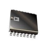
| 描述 | IC DAC 16BIT OCT 2.5V 16TSSOP数模转换器- DAC Octal 16-bit 8CH SPI VOUT |
| 产品分类 | |
| 品牌 | Analog Devices |
| 产品手册 | |
| 产品图片 |
|
| rohs | 符合RoHS无铅 / 符合限制有害物质指令(RoHS)规范要求 |
| 产品系列 | 数据转换器IC,数模转换器- DAC,Analog Devices AD5668BRUZ-3denseDAC |
| 数据手册 | |
| 产品型号 | AD5668BRUZ-3 |
| PCN设计/规格 | |
| 产品培训模块 | http://www.digikey.cn/PTM/IndividualPTM.page?site=cn&lang=zhs&ptm=26125http://www.digikey.cn/PTM/IndividualPTM.page?site=cn&lang=zhs&ptm=26140http://www.digikey.cn/PTM/IndividualPTM.page?site=cn&lang=zhs&ptm=26150http://www.digikey.cn/PTM/IndividualPTM.page?site=cn&lang=zhs&ptm=26147 |
| 产品目录页面 | |
| 产品种类 | 数模转换器- DAC |
| 位数 | 16 |
| 供应商器件封装 | 16-TSSOP |
| 其它名称 | AD5668BRUZ3 |
| 分辨率 | 16 bit |
| 包装 | 管件 |
| 商标 | Analog Devices |
| 安装类型 | 表面贴装 |
| 安装风格 | SMD/SMT |
| 封装 | Tube |
| 封装/外壳 | 16-TSSOP(0.173",4.40mm 宽) |
| 封装/箱体 | TSSOP-16 |
| 工作温度 | -40°C ~ 105°C |
| 工厂包装数量 | 96 |
| 建立时间 | 2.5µs |
| 接口类型 | SPI |
| 数据接口 | DSP,MICROWIRE™,QSPI™,串行,SPI™ |
| 最大功率耗散 | 2.15 mW |
| 最大工作温度 | + 105 C |
| 最小工作温度 | - 40 C |
| 标准包装 | 1 |
| 电压参考 | Internal, External |
| 电压源 | 单电源 |
| 电源电压-最大 | 5.5 V |
| 电源电压-最小 | 2.7 V |
| 积分非线性 | +/- 16 LSB |
| 稳定时间 | 6 us |
| 系列 | AD5668 |
| 结构 | Resistor String |
| 转换器数 | 8 |
| 转换器数量 | 8 |
| 输出数和类型 | 8 电压,单极 |
| 输出类型 | Voltage |
| 采样比 | 95 kSPs |
| 采样率(每秒) | - |


- 商务部:美国ITC正式对集成电路等产品启动337调查
- 曝三星4nm工艺存在良率问题 高通将骁龙8 Gen1或转产台积电
- 太阳诱电将投资9.5亿元在常州建新厂生产MLCC 预计2023年完工
- 英特尔发布欧洲新工厂建设计划 深化IDM 2.0 战略
- 台积电先进制程称霸业界 有大客户加持明年业绩稳了
- 达到5530亿美元!SIA预计今年全球半导体销售额将创下新高
- 英特尔拟将自动驾驶子公司Mobileye上市 估值或超500亿美元
- 三星加码芯片和SET,合并消费电子和移动部门,撤换高东真等 CEO
- 三星电子宣布重大人事变动 还合并消费电子和移动部门
- 海关总署:前11个月进口集成电路产品价值2.52万亿元 增长14.8%


PDF Datasheet 数据手册内容提取
Octal, 16-Bit DAC with 5 ppm/°C On-Chip Reference in 16-Lead TSSOP Enhanced Product AD5668-EP FEATURES FUNCTIONAL BLOCK DIAGRAM Enhanced product features VDD VREFIN/VREFOUT Supports defense and aerospace applications (AQEC) AD5668-EP 1.25RVE/F2.5V Military temperature range (−55°C to +125°C) LDAC REINGPISUTTER REGDIASCTER SDTARCIN AG BUFFER VOUTA Controlled manufacturing baseline One assembly/test site REINGPISUTTER REGDIASCTER SDTARCIN BG BUFFER VOUTB One fabrication site SCLK REINGPISUTTER REGDIASCTER SDTARCIN CG BUFFER VOUTC Product change notification SYNC INTLEORGFIACCE REINGPISUTTER REGDIASCTER SDTARCIN DG BUFFER VOUTD Qualification data available on request Low power, smallest pin-compatible octal DAC: 16 bits DIN REINGPISUTTER REGDIASCTER SDTARCIN EG BUFFER VOUTE 16-lead TSSOP REINGPISUTTER REGDIASCTER SDTARCIN FG BUFFER VOUTF On-chip 1.25 V, 5 ppm/°C reference REINGPISUTTER REGDIASCTER SDTARCIN GG BUFFER VOUTG Power down to 400 nA at 5 V, 200 nA at 3 V 2.7 V to 5.5 V power supply REINGPISUTTER REGDIASCTER SDTARCIN HG BUFFER VOUTH Guaranteed monotonic by design PORWEESRE-TON POWLEORG-DICOWN P3o pwoewre-or-nd roewsent f tuon zcetiroon ssc ale or midscale 1RU-16 PALCDKAACG1EC OLNRL1Y GND 09463-001 Figure 1. Hardware LDAC and LDAC override function CLR function to programmable code Rail-to-rail operation APPLICATIONS Process control Data acquisition systems Portable battery-powered instruments GENERAL DESCRIPTION The AD5668-EP is a low power, octal, 16-bit, buffered voltage- DAC channels to simultaneously update. There is also an output digital-to-analog converter (DAC). It operates from a asynchronous CLR that updates all DACs to a user- single 2.7 V to 5.5 V supply and is guaranteed monotonic programmable code—zero scale, midscale, or full scale. by design. The AD5668-EP uses a versatile 3-wire serial interface that The AD5668-EP has an on-chip reference with an internal gain operates at clock rates up to 50 MHz and is compatible with of 2. The AD5668-EP has a 1.25 V, 5 ppm/°C reference, giving a standard SPI, QSPI, MICROWIRE, and DSP interface standards. full-scale output range of 2.5 V. The on-board reference is off at Additional application and technical information can be found power-up, allowing the use of an external reference, and the in the AD5668 data sheet. internal reference is enabled via a software write. PRODUCT HIGHLIGHTS The part incorporates a power-on-reset circuit that ensures that 1. Octal, 16-bit DAC. the DAC output powers up to 0 V and remains powered up at this 2. On-chip 1.25 V/2.5 V, 5 ppm/°C reference. level until a valid write takes place. The part contains a power- 3. Available in 16-lead TSSOP. down feature that reduces the current consumption of the device 4. Power-on reset to 0 V or midscale. to 400 nA at 5 V and provides software-selectable output loads 5. Power-down capability. When powered down, the DAC while in power-down mode for any or all DAC channels. The typically consumes 200 nA at 3 V and 400 nA at 5 V. outputs of all DACs can be updated simultaneously using the LDAC function, with the added functionality of user-selectable Rev. B Document Feedback Information furnished by Analog Devices is believed to be accurate and reliable. However, no responsibility is assumed by Analog Devices for its use, nor for any infringements of patents or other One Technology Way, P.O. Box 9106, Norwood, MA 02062-9106, U.S.A. rights of third parties that may result from its use. Specifications subject to change without notice. No license is granted by implication or otherwise under any patent or patent rights of Analog Devices. Tel: 781.329.4700 ©2010–2018 Analog Devices, Inc. All rights reserved. Trademarks and registered trademarks are the property of their respective owners. Technical Support www.analog.com
AD5668-EP Enhanced Product TABLE OF CONTENTS Features .............................................................................................. 1 Timing Characteristics .................................................................5 Applications ....................................................................................... 1 Absolute Maximum Ratings ............................................................6 Functional Block Diagram .............................................................. 1 ESD Caution...................................................................................6 General Description ......................................................................... 1 Pin Configuration and Function Descriptions ..............................7 Product Highlights ........................................................................... 1 Typical Performance Characteristics ..............................................8 Revision History ............................................................................... 2 Outline Dimensions ....................................................................... 14 Specifications ..................................................................................... 3 Ordering Guide .......................................................................... 14 AC Characteristics ........................................................................ 4 REVISION HISTORY 1/2018—Rev. A to Rev. B Change to Features Section ............................................................. 1 Changes to Table 5 ............................................................................ 7 Changes to Figure 23 ...................................................................... 11 Moved Figure 33 ............................................................................. 13 Changes to Ordering Guide .......................................................... 14 1/2015—Rev. 0 to Rev. A Changes to Ordering Guide .......................................................... 14 10/2010—Revision 0: Initial Version Rev. B | Page 2 of 14
Enhanced Product AD5668-EP SPECIFICATIONS V = 4.5 V to 5.5 V, R = 2 kΩ to GND, C = 200 pF to GND, V = V . All specifications T to T , unless otherwise noted. DD L L REFIN DD MIN MAX Temperature range is −55°C to +125°C, typical at +25°C. Table 1. Parameter Min Typ Max Unit Conditions/Comments STATIC PERFORMANCE1 Resolution 16 Bits Relative Accuracy ±8 ±21 LSB See Figure 4 Differential Nonlinearity ±1 LSB Guaranteed monotonic by design (see Figure 7) Zero-Code Error 1 14 mV All 0s loaded to DAC register (see Figure 9) Zero-Code Error Drift ±2 µV/°C Full-Scale Error −0.2 −1 % FSR All 1s loaded to DAC register (see Figure 10) Gain Error ±1 % FSR Gain Temperature Coefficient ±2.5 ppm Of FSR/°C Offset Error ±1 ±14 mV DC Power Supply Rejection Ratio –80 dB V ± 10% DD DC Crosstalk (External Reference) 10 µV Due to full-scale output change, R = 2 kΩ to GND or V L DD 5 µV/mA Due to load current change 10 µV Due to powering down (per channel) DC Crosstalk (Internal Reference) 25 µV Due to full-scale output change, R = 2 kΩ to GND or V L DD 10 µV/mA Due to load current change OUTPUT CHARACTERISTICS2 Output Voltage Range 0 V V DD Capacitive Load Stability 2 nF R = ∞ L 10 nF R = 2 kΩ L DC Output Impedance 0.5 Ω Short-Circuit Current 30 mA V = 5 V DD Power-Up Time 4 µs Coming out of power-down mode, V = 5 V DD REFERENCE INPUTS Reference Current 40 55 µA V = V = 5.5 V (per DAC channel) REF DD Reference Input Range 0 V V DD Reference Input Impedance 14.6 kΩ REFERENCE OUTPUT Output Voltage 1.247 1.253 V At ambient Reference Temperature Coefficient2 ±5 ppm/°C Reference Output Impedance 7.5 kΩ LOGIC INPUTS2 Input Current ±3 µA All digital inputs Input Low Voltage, V 0.8 V V = 5 V INL DD Input High Voltage, V 2 V V = 5 V INH DD Pin Capacitance 3 pF POWER REQUIREMENTS V 4.5 5.5 V All digital inputs at 0 or V , DAC active, excludes load current DD DD I (Normal Mode)3 V = V and V = GND DD IH DD IL V = 4.5 V to 5.5 V 1.3 1.8 mA Internal reference off DD V = 4.5 V to 5.5 V 2 2.6 mA Internal reference on DD I (All Power-Down Modes)4 DD V = 4.5 V to 5.5 V 0.4 1 µA V = V and V = GND DD IH DD IL 1 Linearity calculated using a reduced code range of AD5668 (Code 512 to 65,024). Output unloaded. 2 Guaranteed by design and characterization; not production tested. 3 Interface inactive. All DACs active. DAC outputs unloaded. 4 All eight DACs powered down. Rev. B | Page 3 of 14
AD5668-EP Enhanced Product AC CHARACTERISTICS V = 2.7 V to 5.5 V, R = 2 kΩ to GND, C = 200 pF to GND, V = V . All specifications T to T , unless otherwise noted. DD L L REFIN DD MIN MAX Temperature range is −55°C to +125°C, typical at +25°C. Table 2. Parameter1 Min Typ Max Unit Conditions/Comments Output Voltage Settling Time 6 10 µs ¼ to ¾ scale settling to ±2 LSB Slew Rate 1.5 V/µs Digital-to-Analog Glitch Impulse 4 nV-sec 1 LSB change around major carry (see Figure 24) Digital Feedthrough 0.1 nV-sec Reference Feedthrough −90 dB V = 2 V ± 0.1 V p-p, frequency = 10 Hz to 20 MHz REF Digital Crosstalk 0.5 nV-sec Analog Crosstalk 2.5 nV-sec DAC-to-DAC Crosstalk 3 nV-sec Multiplying Bandwidth 340 kHz V = 2 V ± 0.2 V p-p REF Total Harmonic Distortion −80 dB V = 2 V ± 0.1 V p-p, frequency = 10 kHz REF Output Noise Spectral Density 120 nV/√Hz DAC code = 0x8400, 1 kHz 100 nV/√Hz DAC code = 0x8400, 10 kHz Output Noise 15 μV p-p 0.1 Hz to 10 Hz 1 Guaranteed by design and characterization; not production tested. Rev. B | Page 4 of 14
Enhanced Product AD5668-EP TIMING CHARACTERISTICS All input signals are specified with tr = tf = 1 ns/V (10% to 90% of V ) and timed from a voltage level of (V + V )/2. See Figure 2. DD IL IH V = 2.7 V to 5.5 V. All specifications T to T , unless otherwise noted. DD MIN MAX Table 3. Limit at T , T MIN MAX Parameter V = 2.7 V to 5.5 V Unit Conditions/Comments DD t 1 20 ns min SCLK cycle time 1 t 8 ns min SCLK high time 2 t 8 ns min SCLK low time 3 t 13 ns min SYNC to SCLK falling edge set-up time 4 t 4 ns min Data setup time 5 t 4 ns min Data hold time 6 t 0 ns min SCLK falling edge to SYNC rising edge 7 t 15 ns min Minimum SYNC high time 8 t 13 ns min SYNC rising edge to SCLK fall ignore 9 t 0 ns min SCLK falling edge to SYNC fall ignore 10 t 10 ns min LDAC pulse width low 11 t 15 ns min SCLK falling edge to LDAC rising edge 12 t 5 ns min CLR pulse width low 13 t 0 ns min SCLK falling edge to LDAC falling edge 14 t 300 ns typ CLR pulse activation time 15 1 Maximum SCLK frequency is 50 MHz at VDD = 2.7 V to 5.5 V. Guaranteed by design and characterization; not production tested. t10 t1 t9 SCLK t8 t4 t3 t2 t7 SYNC t6 t5 DIN DB31 DB0 t14 t11 LDAC1 t12 LDAC2 CLR t13 VOUT t15 12ASYSNYCNCHRHORONNOOUUS SL DLDAACC U UPDPDAATET EM MOODDE.E. 09463-002 Figure 2. Serial Write Operation Rev. B | Page 5 of 14
AD5668-EP Enhanced Product ABSOLUTE MAXIMUM RATINGS T = 25°C, unless otherwise noted. Stresses at or above those listed under Absolute Maximum A Ratings may cause permanent damage to the product. This is a Table 4. stress rating only; functional operation of the product at these Parameter Rating or any other conditions above those indicated in the operational V to GND −0.3 V to +7 V DD section of this specification is not implied. Operation beyond Digital Input Voltage to GND −0.3 V to V + 0.3 V DD the maximum operating conditions for extended periods may V to GND −0.3 V to V + 0.3 V OUT DD affect product reliability. V /V to GND −0.3 V to V + 0.3 V REFIN REFOUT DD Operating Temperature Range ESD CAUTION Industrial −55°C to +125°C Storage Temperature Range −65°C to +150°C Junction Temperature (T ) 150°C JMAX TSSOP Package Power Dissipation (TJ MAX − TA)/θJA θ Thermal Impedance 150.4°C/W JA Reflow Soldering Peak Temperature SnPb 240°C Pb-Free 260°C Rev. B | Page 6 of 14
Enhanced Product AD5668-EP PIN CONFIGURATION AND FUNCTION DESCRIPTIONS LDAC 1 16 SCLK SYNC 2 15 DIN VDD 3 14 GND VOUTA 4 AD5668-EP 13 VOUTB TOP VIEW VOUTC 5 (Not to Scale) 12 VOUTD VOUTE 6 11 VOUTF VOUTG 7 10 VOUTH VREFIN/VREFOUT 8 9 CLR 09463-003 Figure 3. Pin Configuration Table 5. Pin Function Descriptions Pin Number Mnemonic Description 1 LDAC Active Low Control Input. Pulsing this pin low allows any or all DAC registers to be updated if the input registers have new data. This allows all DAC outputs to update simultaneously. Alternatively, this pin can permanently be tied low. 2 SYNC Active Low Control Input. This is the frame synchronization signal for the input data. When SYNC goes low, it powers on the SCLK and DIN buffers and enables the input shift register. Data is transferred in on the falling edges of the next 32 clocks. If SYNC is taken high before the 32nd falling edge, the rising edge of SYNC acts as an interrupt and the write sequence is ignored by the device. 3 V Power Supply Input. This device can be operated from 2.7 V to 5.5 V, and it is recommended the supply be DD decoupled with a 10 µF capacitor in parallel with a 0.1 µF capacitor to GND. 4 V A Analog Output Voltage from DAC A. The output amplifier has rail-to-rail operation. OUT 5 V C Analog Output Voltage from DAC C. The output amplifier has rail-to-rail operation. OUT 6 V E Analog Output Voltage from DAC E. The output amplifier has rail-to-rail operation. OUT 7 V G Analog Output Voltage from DAC G. The output amplifier has rail-to-rail operation. OUT 8 V / Common Pin for Reference Input and Reference Output. When using the internal reference, this is the REFIN V reference output pin. When using an external reference, this is the reference input pin. The default for this REFOUT pin is a reference input. 9 CLR Asynchronous Clear Input. The CLR input is falling edge sensitive. When CLR is low, all LDAC pulses are ignored. When CLR is activated, the input register and the DAC register are updated with the data contained in the CLR code register: zero, midscale, or full-scale. Default setting clears the output to 0 V. 10 V H Analog Output Voltage from DAC H. The output amplifier has rail-to-rail operation. OUT 11 V F Analog Output Voltage from DAC F. The output amplifier has rail-to-rail operation. OUT 12 V D Analog Output Voltage from DAC D. The output amplifier has rail-to-rail operation. OUT 13 V B Analog Output Voltage from DAC B. The output amplifier has rail-to-rail operation. OUT 14 GND Ground Reference Point for All Circuitry on the Device. 15 DIN Serial Data Input. This device has a 32-bit shift register. Data is clocked into the register on the falling edge of the serial clock input. 16 SCLK Serial Clock Input. Data is clocked into the input shift register on the falling edge of the serial clock input. Data can be transferred at rates of up to 50 MHz. Rev. B | Page 7 of 14
AD5668-EP Enhanced Product TYPICAL PERFORMANCE CHARACTERISTICS 10 1.0 8 VTAD D= =2 5V°RCEF = 5V 0.8 VVDRDEF =O U3TV = 1.25V 6 TA = 25°C 0.6 4 0.4 B) B) S 2 S L L 0.2 R ( R ( RO 0 RO 0 R R E –2 E L L –0.2 N N I–4 D –0.4 –6 –0.6 –8 –0.8 –100 5k 10k 15k 20k 25k 3C0kOD3E5k 40k 45k 50k 55k 60k 65k 09463-004 –1.00 5000 10000 15000 20000 25000 30000COD35000E 40000 45000 50000 55000 60000 6500009463-007 Figure 4. INL—External Reference Figure 7. DNL 1.0 10 VDD = 3V 0.8 8 VREFOUT = 1.25V TA = 25°C 0.6 6 0.4 4 OR (LSB) 20 R (% FSR) 0.20 FULL-SCALE ERROR GAIN ERROR R O L ER –2 ERR –0.2 N I –4 –0.4 –0.6 –6 –0.8 –8 –100 5000 10000 15000 20000 25000 30000COD35000E 40000 45000 50000 55000 60000 6500009463-005 –1.0–55 –35 –15 5TEMP2E5RATU4R5E (°C6)5 85 105 125 09463-008 Figure 5. INL Figure 8. Gain Error and Full-Scale Error vs. Temperature 1.0 1.5 VDD = VREF = 5V 0.8 TA = 25°C 1.0 0.6 0.5 0.4 B) ZERO-SCALE ERROR LS 0.2 V) 0 ROR ( 0 OR (m –0.5 NL ER –0.2 ERR –1.0 OFFSET ERROR D –0.4 –1.5 –0.6 –2.0 –0.8 –1.00 10k 20k 30CkODE 40k 50k 60k 09463-006 –2.5–55 –35 –15 5TEMP2E5RATU4R5E (°C6)5 85 105 125 09463-009 Figure 6. DNL—External Reference Figure 9. Zero-Scale Error and Offset Error vs. Temperature Rev. B | Page 8 of 14
Enhanced Product AD5668-EP 1.0 14 VDD = 3.6V VDD = 5.5V 12 0.5 GAIN ERROR 10 % FSR) 0 FULL-SCALE ERROR ENCY 8 VREFOUT = 1.25V VREFOUT = 2.5V R ( –0.5 QU O E 6 R R R F E –1.0 4 –1.5 2 –2.02.7 3.2 3.7 VDD 4(V.2) 4.7 5.2 09463-010 02.022.042.062.082.102.122ID.1D4 (m2.A16)2.182.202.222.242.262.28 09463-013 Figure 10. Gain Error and Full-Scale Error vs. Supply Voltage (VDD) Figure 13. IDD Histogram with Internal Reference 1.0 0.5 TA = 25°C DAC LOADED WITH DAC LOADED WITH 0.4 FULL-SCALE ZERO-SCALE 0.5 ZERO-SCALE ERROR SOURCING CURRENT SINKING CURRENT 0.3 0 V) 0.2 V) GE ( 0.1 VDD= 3V ERROR (m ––10..05 OR VOLTA –0.10 VREFOUT = 1.25V R R –1.5 E –0.2 –0.3 VDD= 5V –2.0 OFFSET ERROR VREFOUT = 2.5V –0.4 –2.52.7 3.2 3.7 VDD 4(V.2) 4.7 5.2 09463-011 –0.5–10 –8 –6 –4 C–2URRE0NT (mA2) 4 6 8 10 09463-014 Figure 11. Zero-Scale Error and Offset Error vs. Supply Voltage (VDD) Figure 14. Headroom at Rails vs. Source and Sink 20 6 1168 VVDDDD == 35..65VV 5 VTVADR DE=F =O2 5U5°VTC = 2.5V FULL SCALE 14 4 3/4 SCALE NCY 12 V) 3 MIDSCALE REQUE 108 V (OUT 2 F 1/4 SCALE 6 1 4 2 0 ZERO SCALE 01.201.221.241.261.281.30ID1D.3 (2m1A.3)41.361.381.401.421.44 09463-012 –1–30 –20 –10 CURRE0NT (mA) 10 20 30 09463-015 Figure 12. IDD Histogram with External Reference Figure 15. Source and Sink Capability Rev. B | Page 9 of 14
AD5668-EP Enhanced Product 2.0 8 TA = 25°C VDD = VREF = 5V TA = 25°C 1.8 7 1.6 6 1.4 1.2 5 I (mA)DD01..80 VDD = VREF = 3V I (mA)DD 34 VDD = 5V 0.6 2 0.4 0.2 1 0512 10512 20512 30C51O2DE 40512 50512 60512 09463-017 00 VDD1 = 3V 2 VLOG3IC (V) 4 5 6 09463-020 Figure 16. Supply Current (IDD) vs. Code Figure 19. Supply Current (IDD) vs. Logic Input Voltage (VLOGIC) 1.6 VDD = VREFIN = 5.5V 1.4 1.2 1.0 VDD = VREFIN = 3.6V VTAD D= =2 5V°RCEF = 5V (mA)DD0.8 F0OAxUNU0LDT0L P02-0US0T0CTp OALF LO0TExAO FDC FEGOFDNDF DEW CITHHA 2NkGΩE I 0.6 0.4 VOUT= 909mV/DIV 1 0.2 0–40 –20 0 TEM2P0ERATU4R0E (°C)60 80 100 09463-018 TIME BASE = 4µs/DIV 09463-021 Figure 17. Supply Current (IDD) vs. Temperature Figure 20. Full-Scale Settling Time, 5 V 1.6 TA=25°C VDD = VREF = 5V 1.4 TA = 25°C 1.2 1.0 A) (mD 0.8 ID VDD 0.6 1 0.4 MAX(C2)* 420.0mV 0.2 2 VOUT 02.7 3.2 3.7 VDD 4(V.2) 4.7 5.2 09463-019 CH1 2.0V CH2 500mV MA 1C0H01µ s 1 215.M28SV/s 8.0ns/pt 09463-022 Figure 18. Supply Current (IDD) vs. Supply Voltage (VDD) Figure 21. Power-On Reset to 0 V Rev. B | Page 10 of 14
Enhanced Product AD5668-EP 2.5000 VDD = VREF = 5V 2.4995 TA = 25°C 2.4990 2.4985 2.4980 VDD V) 1 (UT 2.4975 O V 2.4970 2.4965 2.4960 VDD = 5V 2 2.4955 VREFOUT = 2.5V VOUT T4nAs =/S 2A5M°CPLE NUMBER CH1 2.0V CH2 1.0V MA 1C0H01µ s 1 215.M28SV/s 8.0ns/pt 09463-023 2.49500 64 128 192 SA2M5P6LE 320 384 448 512 09463-026 Figure 22. Power-On Reset to Midscale Figure 25. Analog Crosstalk 2.4900 SYNC 2.4895 1 SCLK 2.4890 3 2.4885 V) 2.4880 (UT O2.4875 V 2.4870 VOUT VDD = 5V 2.4865 VDD = 5V 2 2.4860 VREFOUT = 2.5V TA = 25°C CCHH13 55..00VV CH2 500mV M400ns A CH1 1.4V 09463-024 2.48550 64 128 192 SA2M5P6LE 342n0s/SAM3P84LE NU4M48BER512 09463-027 Figure 23. Exiting Power-Down to Midscale Figure 26. DAC-to-DAC Crosstalk 2.505 222...555000234 TVVADR DE=F =O2 5U5°TVC = 2.5V VTDADA DC= =2L 5VO°RACEDFE =D 5 WVITH MIDSCALE 2.501 4ns/SAMPLE NUMBER 2.500 GLITCH IMPULSE = 3.55nV-s 2.499 1 LSB CHANGE AROUND 2.498 MIDSCALE (0x8000 TO 0x7FFF) 2.497 (V)OUT222...444999456 V/DIV 1 V µ 2.493 2 2.492 2.491 2.490 2.489 2.488 2.487 22..4488560 64 128 192 SA2M5P6LE 320 384 448 512 09463-025 4s/DIV 09463-028 Figure 24. Digital-to-Analog Glitch Impulse (Negative) Figure 27. 0.1 Hz to 10 Hz Output Noise Plot, External Reference Rev. B | Page 11 of 14
AD5668-EP Enhanced Product –20 TVVADR DE=F =O2 5U5°TVC = 2.5V –30 TVDADA DC= =2L 55O°VACDED WITH FULL SCALE DAC LOADED WITH MIDSCALE VREF = 2V ± 0.3V p-p –40 –50 V 0µV/DI1 (dB) –60 1 –70 –80 –90 5s/DIV 09463-029 –100 2k F4RkEQUENCY 6(Hkz) 8k 10k 09463-032 Figure 28. 0.1 Hz to 10 Hz Output Noise Plot, Internal Reference Figure 31. Total Harmonic Distortion 16 VDD = 3V VREF = VDD VTAR E=F O25U°TC = 1.25V 14 TA = 25°C DAC LOADED WITH MIDSCALE VDD=3V 12 V s) µV/DI1 ME (µ10 5 TI 8 VDD=5V 6 4s/DIV 09463-030 40 1 2 3 CA4PACITA5NCE 6(nF) 7 8 9 10 09463-033 Figure 29. 0.1 Hz to 10 Hz Output Noise Plot, Internal Reference Figure 32. Settling Time vs. Capacitive Load 800 TA = 25°C MIDSCALE LOADED 700 600 Hz) V/ 500 n E ( S OI 400 N T PU 300 UT VDD= 5V O 200 VREFOUT = 2.5V 100 VDD= 3V VREFOUT = 1.25V 0100 1k FREQU1E0NkCY (Hz) 100k 1M 09463-031 Figure 30. Noise Spectral Density, Internal Reference Rev. B | Page 12 of 14
Enhanced Product AD5668-EP 5 VDD = 5V 0 TA = 25°C CLR 3 –5 –10 VOUTF –15 B) d ( –20 –25 VOUTB –30 44 –35 2 CH3 5.0V CCHH42 11..00VV M200ns A CH3 1.10V 09463-034 –4010k 100kFREQUENCY (Hz)1M 10M 09463-035 Figure 33. Hardware CLR Figure 34. Multiplying Bandwidth Rev. B | Page 13 of 14
AD5668-EP Enhanced Product OUTLINE DIMENSIONS 5.10 5.00 4.90 16 9 4.50 6.40 4.40 BSC 4.30 1 8 PIN 1 1.20 MAX 0.15 0.20 0.05 0.09 0.75 0.30 8° 0.60 B0.S6C5 0.19 SEATING 0° 0.45 PLANE COPLANARITY 0.10 COMPLIANT TO JEDEC STANDARDS MO-153-AB Figure 35. 16-Lead Thin Shrink Small Outline Package [TSSOP] (RU-16) Dimensions shown in millimeters ORDERING GUIDE Power-On Internal Package Model1 Reset to Code Accuracy LSB (INL) Reference (V) Temperature Range Package Description Option AD5668SRU-EP-1 Zero ±21 1.25 −55°C to +125°C 16-Lead TSSOP RU-16 AD5668SRU-EP-1RL7 Zero ±21 1.25 −55°C to +125°C 16-Lead TSSOP RU-16 AD5668SRUZ-EP-1 Zero ±21 1.25 −55°C to +125°C 16-Lead TSSOP RU-16 AD5668SRUZ-EP-1RL7 Zero ±21 1.25 −55°C to +125°C 16-Lead TSSOP RU-16 1 Z= RoHS Compliant Part. ©2010–2018 Analog Devices, Inc. All rights reserved. Trademarks and registered trademarks are the property of their respective owners. D09463-0-1/18(B) Rev. B | Page 14 of 14
Mouser Electronics Authorized Distributor Click to View Pricing, Inventory, Delivery & Lifecycle Information: A nalog Devices Inc.: EVAL-AD5668SDCZ EVAL-AD5668SDRZ AD5668BRUZ-3 AD5668ARUZ-3 AD5668BCPZ-1500RL7 AD5668BCPZ-1-RL7 AD5668BRUZ-1REEL7 AD5668BRUZ-3REEL7 AD5668BRUZ-2 AD5668ACPZ-2-RL7 AD5668BRUZ-1 AD5668ARUZ-2 AD5668ARUZ-3REEL7 AD5668SRU-EP-1RL7 AD5668ARUZ-2REEL7 AD5668BRUZ-2REEL7 AD5668BCBZ-1-RL7 AD5668ACPZ-3-RL7 AD5668BCPZ-2-RL7 AD5668BCBZ-3-RL7 AD5668SRU-EP-1 AD5668SRUZ-EP-1RL7 AD5668SRUZ-EP-1