ICGOO在线商城 > 集成电路(IC) > 数据采集 - 数模转换器 > TLC5620ID
 Datasheet下载
- 型号: TLC5620ID
- 制造商: Texas Instruments
- 库位|库存: xxxx|xxxx
- 要求:
| 数量阶梯 | 香港交货 | 国内含税 |
| +xxxx | $xxxx | ¥xxxx |
查看当月历史价格
查看今年历史价格
TLC5620ID产品简介:
ICGOO电子元器件商城为您提供TLC5620ID由Texas Instruments设计生产,在icgoo商城现货销售,并且可以通过原厂、代理商等渠道进行代购。 TLC5620ID价格参考。Texas InstrumentsTLC5620ID封装/规格:数据采集 - 数模转换器, 8 位 数模转换器 4 14-SOIC。您可以下载TLC5620ID参考资料、Datasheet数据手册功能说明书,资料中有TLC5620ID 详细功能的应用电路图电压和使用方法及教程。
Texas Instruments(德州仪器)的TLC5620ID是一款8位数模转换器(DAC),广泛应用于各种数据采集系统中。它具有低功耗、高精度和多通道的特点,适用于需要将数字信号转换为模拟信号的场景。以下是TLC5620ID的一些典型应用场景:

1. 工业自动化与控制:在工业控制系统中,TLC5620ID可以用于将来自微控制器或处理器的数字指令转换为模拟信号,以驱动执行器、传感器或其他模拟设备。例如,在温度控制、压力调节和电机控制等应用中,TLC5620ID能够精确地生成所需的模拟电压或电流信号。

2. 通信系统:在通信设备中,TLC5620ID可用于生成调制信号或参考电压。它可以作为信号发生器的一部分,帮助实现调幅(AM)、调频(FM)等调制方式,或者用于生成基准电压以确保系统的稳定性和准确性。

3. 音频处理:TLC5620ID还可以应用于音频设备中,如音响系统、耳机放大器和语音识别设备。通过将数字音频信号转换为模拟音频信号,TLC5620ID可以驱动扬声器或耳机,提供高质量的音频输出。

4. 医疗设备:在医疗领域,TLC5620ID可用于心电图机、超声波设备和其他诊断仪器中。它能够将数字信号转换为模拟信号,以便进行进一步的信号处理和显示。此外,TLC5620ID的低功耗特性使得它非常适合便携式医疗设备。

5. 测试与测量仪器:在实验室和生产环境中,TLC5620ID常用于校准和测试设备中。它可以生成精确的模拟信号,用于验证传感器、示波器和其他测量仪器的性能。此外,TLC5620ID的多通道设计使其能够在同一设备中同时处理多个信号源。

总之,TLC5620ID凭借其高性能和灵活性,适用于多种数据采集和信号处理场景,尤其适合那些需要高效、精确地进行数模转换的应用。
| 参数 | 数值 |
| 产品目录 | 集成电路 (IC)半导体 |
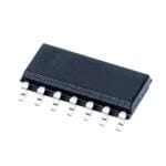
| 描述 | IC QUAD 8-BIT D/A CONV 14-SOIC数模转换器- DAC Quad 8bit DigitAL/AN |
| 产品分类 | |
| 品牌 | Texas Instruments |
| 产品手册 | |
| 产品图片 |
|
| rohs | 符合RoHS无铅 / 符合限制有害物质指令(RoHS)规范要求 |
| 产品系列 | 数据转换器IC,数模转换器- DAC,Texas Instruments TLC5620ID- |
| 数据手册 | |
| 产品型号 | TLC5620ID |
| 产品培训模块 | http://www.digikey.cn/PTM/IndividualPTM.page?site=cn&lang=zhs&ptm=13240 |
| 产品目录页面 | |
| 产品种类 | 数模转换器- DAC |
| 位数 | 8 |
| 供应商器件封装 | 14-SOIC |
| 其它名称 | 296-1339-5 |
| 分辨率 | 8 bit |
| 制造商产品页 | http://www.ti.com/general/docs/suppproductinfo.tsp?distId=10&orderablePartNumber=TLC5620ID |
| 包装 | 管件 |
| 单位重量 | 133.400 mg |
| 商标 | Texas Instruments |
| 安装类型 | 表面贴装 |
| 安装风格 | SMD/SMT |
| 封装 | Tube |
| 封装/外壳 | 14-SOIC(0.154",3.90mm 宽) |
| 封装/箱体 | SOIC-14 |
| 工作温度 | -40°C ~ 85°C |
| 工厂包装数量 | 50 |
| 建立时间 | 10µs |
| 接口类型 | Serial (3-Wire) |
| 数据接口 | 串行 |
| 最大工作温度 | + 85 C |
| 最小工作温度 | - 40 C |
| 标准包装 | 50 |
| 电压参考 | External |
| 电压源 | 单电源 |
| 电源电压-最大 | 5.25 V |
| 电源电压-最小 | 4.75 V |
| 积分非线性 | +/- 1 LSB |
| 稳定时间 | 10 us |
| 系列 | TLC5620 |
| 结构 | Resistor-String |
| 转换器数 | 4 |
| 转换器数量 | 4 |
| 输出数和类型 | 4 电压,单极 |
| 输出类型 | Voltage |
| 采样比 | 48 kSPs |
| 采样率(每秒) | 48k |


- 商务部:美国ITC正式对集成电路等产品启动337调查
- 曝三星4nm工艺存在良率问题 高通将骁龙8 Gen1或转产台积电
- 太阳诱电将投资9.5亿元在常州建新厂生产MLCC 预计2023年完工
- 英特尔发布欧洲新工厂建设计划 深化IDM 2.0 战略
- 台积电先进制程称霸业界 有大客户加持明年业绩稳了
- 达到5530亿美元!SIA预计今年全球半导体销售额将创下新高
- 英特尔拟将自动驾驶子公司Mobileye上市 估值或超500亿美元
- 三星加码芯片和SET,合并消费电子和移动部门,撤换高东真等 CEO
- 三星电子宣布重大人事变动 还合并消费电子和移动部门
- 海关总署:前11个月进口集成电路产品价值2.52万亿元 增长14.8%


PDF Datasheet 数据手册内容提取
TLC5620C, TLC5620I QUADRUPLE 8-BIT DIGITAL-TO-ANALOG CONVERTERS SLAS081E – NOVEMBER 1994 – REVISED NOVEMBER 2001 (cid:0) Four 8-Bit Voltage Output DACs N OR D PACKAGE (cid:0) (TOP VIEW) 5-V Single-Supply Operation (cid:0) Serial Interface GND 1 14 VDD (cid:0) High-Impedance Reference Inputs REFA 2 13 LDAC (cid:0) Programmable 1 or 2 Times Output Range REFB 3 12 DACA (cid:0) REFC 4 11 DACB Simultaneous Update Facility (cid:0) REFD 5 10 DACC Internal Power-On Reset DATA 6 9 DACD (cid:0) Low-Power Consumption CLK 7 8 LOAD (cid:0) Half-Buffered Output applications (cid:0) Programmable Voltage Sources (cid:0) Digitally Controlled Amplifiers/Attenuators (cid:0) Mobile Communications (cid:0) Automatic Test Equipment (cid:0) Process Monitoring and Control (cid:0) Signal Synthesis description The TLC5620C and TLC5620I are quadruple 8-bit voltage output digital-to-analog converters (DACs) with buffered reference inputs (high impedance). The DACs produce an output voltage that ranges between either one or two times the reference voltages and GND, and the DACs are monotonic. The device is simple to use, running from a single supply of 5 V. A power-on reset function is incorporated to ensure repeatable start-up conditions. Digital control of the TLC5620C and TLC5620I are over a simple three-wire serial bus that is CMOS compatible and easily interfaced to all popular microprocessor and microcontroller devices. The 11-bit command word comprises eightbits of data, two DAC-select bits, and a range bit, the latter allowing selection between the times 1 or times 2 output range. The DAC registers are double buffered, allowing a complete set of new values to be written to the device, then all DAC outputs are updated simultaneously through control of LDAC. The digital inputs feature Schmitt triggers for high noise immunity. The 14-terminal small-outline (D) package allows digital control of analog functions in space-critical applications. The TLC5620C is characterized for operation from 0°C to 70°C. The TLC5620I is characterized for operation from –40°C to 85°C. The TLC5620C and TLC5620I do not require external trimming. AVAILABLE OPTIONS PACKAGE SMALL OUTLINE PLASTIC DIP TA (D) (N) 0°C to 70°C TLC5620CD TLC5620CN –40°C to 85°C TLC5620ID TLC5620IN Please be aware that an important notice concerning availability, standard warranty, and use in critical applications of TexasInstruments semiconductor products and disclaimers thereto appears at the end of this data sheet. PRODUCTION DATA information is current as of publication date. Copyright 2001, Texas Instruments Incorporated Products conform to specifications per the terms of Texas Instruments standard warranty. Production processing does not necessarily include testing of all parameters. POST OFFICE BOX 655303 • DALLAS, TEXAS 75265 1
TLC5620C, TLC5620I QUADRUPLE 8-BIT DIGITAL-TO-ANALOG CONVERTERS SLAS081E – NOVEMBER 1994 – REVISED NOVEMBER 2001 functional block diagram 2 REFA + – DAC + 12 8 Latch Latch 8 × 2 – DACA 3 REFB + – DAC + 11 8 Latch Latch 8 × 2 – DACB 4 REFC + – DAC + 10 8 Latch Latch 8 × 2 – DACC 5 REFD + – DAC + 9 8 Latch Latch 8 × 2 – DACD 7 CLK 6 Serial Power-On DATA 13 8 Interface Reset LOAD LDAC Terminal Functions TERMINAL II//OO DDEESSCCRRIIPPTTIIOONN NAME NO. CLK 7 I Serial interface clock. The input digital data is shifted into the serial interface register on the falling edge of the clock applied to the CLK terminal. DACA 12 O DAC A analog output DACB 11 O DAC B analog output DACC 10 O DAC C analog output DACD 9 O DAC D analog output DATA 6 I Serial interface digital data input. The digital code for the DAC is clocked into the serial interface register serially. Each data bit is clocked into the register on the falling edge of the clock signal. GND 1 I Ground return and reference terminal LDAC 13 I Load DAC. When the LDAC signal is high, no DAC output updates occur when the input digital data is read into the serial interface. The DAC outputs are only updated when LDAC is taken from high to low. LOAD 8 I Serial Interface load control. When LDAC is low, the falling edge of the LOAD signal latches the digital data into the output latch and immediately produces the analog voltage at the DAC output terminal. REFA 2 I Reference voltage input to DAC A. This voltage defines the output analog range. REFB 3 I Reference voltage input to DAC B. This voltage defines the output analog range. REFC 4 I Reference voltage input to DAC C. This voltage defines the output analog range. REFD 5 I Reference voltage input to DAC D. This voltage defines the output analog range. VDD 14 I Positive supply voltage 2 POST OFFICE BOX 655303 • DALLAS, TEXAS 75265
TLC5620C, TLC5620I QUADRUPLE 8-BIT DIGITAL-TO-ANALOG CONVERTERS SLAS081E – NOVEMBER 1994 – REVISED NOVEMBER 2001 detailed description The TLC5620 is implemented using four resistor-string DACs. The core of each DAC is a single resistor with 256 taps, corresponding to the 256 possible codes listed in Table 1. One end of each resistor string is connected to the GND terminal and the other end is fed from the output of the reference input buffer. Monotonicity is maintained by use of the resistor strings. Linearity depends upon the matching of the resistor elements and upon the performance of the output buffer. Since the inputs are buffered, the DACs always present a high-impedance load to the reference source. Each DAC output is buffered by a configurable-gain output amplifier that can be programmed to times 1 or times 2 gain. On power up, the DACs are reset to CODE 0. Each output voltage is given by: V (DACA|B|C|D)(cid:2)REF(cid:0)CODE(cid:0)(1(cid:1)RNG bit value) O 256 where CODE is in the range 0 to 255 and the range (RNG) bit is 0 or 1 within the serial control word. Table 1. Ideal Output Transfer D7 D6 D5 D4 D3 D2 D1 D0 OUTPUT VOLTAGE 0 0 0 0 0 0 0 0 GND 0 0 0 0 0 0 0 1 (1/256) × REF (1+RNG) • • • • • • • • • • • • • • • • • • 0 1 1 1 1 1 1 1 (127/256) × REF (1+RNG) 1 0 0 0 0 0 0 0 (128/256) × REF (1+RNG) • • • • • • • • • • • • • • • • • • 1 1 1 1 1 1 1 1 (255/256) × REF (1+RNG) data interface With LOAD high, data is clocked into the DATA terminal on each falling edge of CLK. Once all data bits have been clocked in, LOAD is pulsed low to transfer the data from the serial input register to the selected DAC as shown in Figure 1. When LDAC is low, the selected DAC output voltage is updated when LOAD goes low. When LDAC is high during serial programming, the new value is stored within the device and can be transferred to the DAC output at a later time by pulsing LDAC low as shown in Figure 2. Data is entered most significant bit (MSB) first. Data transfers using two 8-clock cycle periods are shown in Figures 3 and 4. CLK tsu(DATA-CLK) tsu(LOAD-CLK) tv(DATA-CLK) DATA A1 A0 RNG D7 D6 D5 D4 D3 D2 D1 D0 tsu(CLK-LOAD) tw(LOAD) LOAD DAC Update Figure 1. LOAD-Controlled Update (LDAC = Low) POST OFFICE BOX 655303 • DALLAS, TEXAS 75265 3
TLC5620C, TLC5620I QUADRUPLE 8-BIT DIGITAL-TO-ANALOG CONVERTERS SLAS081E – NOVEMBER 1994 – REVISED NOVEMBER 2001 CLK tsu(DATA-CLK) tv(DATA-CLK) DATA A1 A0 RNG D7 D6 D5 D4 D3 D2 D1 D0 tsu(LOAD-LDAC) LOAD tw(LDAC) LDAC DAC Update Figure 2. LDAC-Controlled Update CLK Low CLK ÎÎÎÎÎÎ ÎÎÎ ÎÎÎ DATA A1 A0 RNG D7 D6 D5 D4 D3 D2 D1 D0 LOAD LDAC Figure 3. Load-Controlled Update Using 8-Bit Serial Word (LDAC = Low) CLK Low CLK ÎÎÎÎÎÎÎ ÎÎÎÎ ÎÎÎÎ DATA A1 A0 RNG D7 D6 D5 D4 D3 D2 D1 D0 LOAD LDAC Figure 4. LDAC-Controlled Update Using 8-Bit Serial Word Table 2 lists the A1 and A0 bits and the selection of the updated DACs. The RNG bit controls the DAC output range. When RNG = low, the output range is between the applied reference voltage and GND, and when RNG = high, the range is between twice the applied reference voltage and GND. Table 2. Serial Input Decode A1 A0 DAC UPDATED 0 0 DACA 0 1 DACB 1 0 DACC 1 1 DACD 4 POST OFFICE BOX 655303 • DALLAS, TEXAS 75265
TLC5620C, TLC5620I QUADRUPLE 8-BIT DIGITAL-TO-ANALOG CONVERTERS SLAS081E – NOVEMBER 1994 – REVISED NOVEMBER 2001 linearity, offset, and gain error using single-end supplies When an amplifier is operated from a single supply, the voltage offset can still be either positive or negative. With a positive offset voltage, the output voltage changes on the first code change. With a negative offset the output voltage may not change with the first code depending on the magnitude of the offset voltage. The output amplifier attempts to drive the output to a negative voltage. However, because the most negative supply rail is ground, the output cannot drive below ground and clamps the output at 0 V. The output voltage then remains at zero until the input code value produces a sufficient positive output voltage to overcome the negative offset voltage, resulting in the transfer function shown in Figure 5. Output Voltage 0 V DAC Code Negative Offset Figure 5. Effect of Negative Offset (Single Supply) This offset error, not the linearity error, produces this breakpoint. The transfer function would have followed the dotted line if the output buffer could drive below ground. For a DAC, linearity is measured between zero-input code (all inputs 0) and full-scale code (all inputs 1) after offset and full scale are adjusted out or accounted for in some way. However, single-supply operation does not allow for adjustment when the offset is negative due to the breakpoint in the transfer function. So the linearity is measured between full-scale code and the lowest code that produces a positive output voltage. The code is calculated from the maximum specification for the negative offset voltage. POST OFFICE BOX 655303 • DALLAS, TEXAS 75265 5
TLC5620C, TLC5620I QUADRUPLE 8-BIT DIGITAL-TO-ANALOG CONVERTERS SLAS081E – NOVEMBER 1994 – REVISED NOVEMBER 2001 equivalent inputs and outputs INPUT CIRCUIT OUTPUT CIRCUIT VDD VDD _ Input from Decoded DAC + DAC Register String Vref × 1 Voltage Output Input Output 84 kΩ To DAC Resistor Range × 2 ISINK String Select 60 µA 84 kΩ Typical GND GND absolute maximum ratings over operating free-air temperature range (unless otherwise noted)† Supply voltage (V – GND) . . . . . . . . . . . . . . . . . . . . . . . . . . . . . . . . . . . . . . . . . . . . . . . . . . . . . . . . . . . . . . . . . 7 V DD Digital input voltage range . . . . . . . . . . . . . . . . . . . . . . . . . . . . . . . . . . . . . . . . . . . . . GND – 0.3 V to V + 0.3 V DD Reference input voltage range, V . . . . . . . . . . . . . . . . . . . . . . . . . . . . . . . . . . . . . . GND – 0.3 V to V + 0.3 V ID DD Operating free-air temperature range, T :TLC5620C . . . . . . . . . . . . . . . . . . . . . . . . . . . . . . . . . . . . 0°C to 70°C A TLC5620I . . . . . . . . . . . . . . . . . . . . . . . . . . . . . . . . . . . –40°C to 85°C Storage temperature range, T . . . . . . . . . . . . . . . . . . . . . . . . . . . . . . . . . . . . . . . . . . . . . . . . . . . –50°C to 150°C stg Lead temperature 1,6 mm (1/16 inch) from case for 10 seconds . . . . . . . . . . . . . . . . . . . . . . . . . . . . . . . 260°C †Stresses beyond those listed under “absolute maximum ratings” may cause permanent damage to the device. These are stress ratings only, and functional operation of the device at these or any other conditions beyond those indicated under “recommended operating conditions” is not implied. Exposure to absolute-maximum-rated conditions for extended periods may affect device reliability. recommended operating conditions MIN NOM MAX UNIT Supply voltage, VDD 4.75 5.25 V High-level input voltage, VIH 0.8 VDD V Low-level input voltage, VIL 0.8 V Reference voltage, Vref [A|B|C|D] VDD–1.5 V Analog full-scale output voltage, RL = 10 kΩ 3.5 V Load resistance, RL 10 kΩ Setup time, data input, tsu(DATA-CLK) (see Figures 1 and 2) 50 ns Valid time, data input valid after CLK↓, tv(DATA-CLK) (see Figures 1 and 2) 50 ns Setup time, CLK eleventh falling edge to LOAD, tsu(CLK-LOAD) (see Figure 1) 50 ns Setup time, LOAD↑ to CLK↓, tsu(LOAD-CLK) (see Figure 1) 50 ns Pulse duration, LOAD, tw(LOAD) (see Figure 1) 250 ns Pulse duration, LDAC, tw(LDAC) (see Figure 2) 250 ns Setup time, LOAD↑ to LDAC↓,tsu(LOAD-LDAC) (see Figure 2) 0 ns CLK frequency 1 MHz TLC5620C 0 70 °C OOppeerraattiinngg ffrreeee-aaiirr tteemmppeerraattuurree, TTAA TLC5620I –40 85 °C 6 POST OFFICE BOX 655303 • DALLAS, TEXAS 75265
TLC5620C, TLC5620I QUADRUPLE 8-BIT DIGITAL-TO-ANALOG CONVERTERS SLAS081E – NOVEMBER 1994 – REVISED NOVEMBER 2001 electrical characteristics over recommended operating free-air temperature range, V = 5 V ±5%, DD V = 2 V, × 1 gain output range (unless otherwise noted) ref PARAMETER TEST CONDITIONS MIN TYP MAX UNIT IIH High-level input current VI = VDD ±10 µA IIL Low-level input current VI = 0 V ±10 µA IO(sink) Output sink current 20 µA EEaacchh DDAACC oouuttppuutt IO(source) Output source current 2 mA Input capacitance 15 CCii ppFF Reference input capacitance 15 IDD Supply current VDD = 5 V 2 mA Iref Reference input current VDD = 5 V, Vref = 2 V ±10 µA EL Linearity error (end point corrected) Vref = 2 V, ×2 gain (see Note 1) ±1 LSB ED Differential-linearity error Vref = 2 V, ×2 gain (see Note 2) ±0.9 LSB EZS Zero-scale error Vref = 2 V, ×2 gain (see Note 3) 0 30 mV Zero-scale-error temperature coefficient Vref = 2 V, ×2 gain (see Note 4) 10 µV/°C EFS Full-scale error Vref = 2 V, ×2 gain (see Note 5) ±60 mV Full-scale-error temperature coefficient Vref = 2 V, ×2 gain (see Note 6) ±25 µV/°C PSRR Power-supply rejection ratio See Notes 7 and 8 0.5 mV/V NOTES: 1. Integral nonlinearity (INL) is the maximum deviation of the output from the line between zero and full scale (excluding the effects of zero code and full-scale errors). 2. Differential nonlinearity (DNL) is the difference between the measured and ideal 1 LSB amplitude change of any two adjacent codes. Monotonic means the output voltage changes in the same direction (or remains constant) as a change in the digital input code. 3. Zero-scale error is the deviation from zero voltage output when the digital input code is zero. 4. Zero-scale-error temperature coefficient is given by: ZSETC = [ZSE(Tmax) – ZSE(Tmin)]/Vref × 106/(Tmax – Tmin). 5. Full-scale error is the deviation from the ideal full-scale output (Vref – 1 LSB) with an output load of 10 kΩ. 6. Full-scale-error temperature coefficient is given by: FSETC = [FSE(Tmax) – FSE (Tmin)]/Vref × 106/(Tmax – Tmin). 7. Zero-scale-error rejection ratio (ZSE RR) is measured by varying the VDD from 4.5 V to 5.5 V dc and measuring the proportion of this signal imposed on the zero-code output voltage. 8. Full-scale-error rejection ratio (FSE RR) is measured by varying the VDD from 4.5 V to 5.5 V dc and measuring the proportion of this signal imposed on the full-scale output voltage. operating characteristics over recommended operating free-air temperature range, V = 5 V ±5%, DD V = 2 V, × 1 gain output range (unless otherwise noted) ref TEST CONDITIONS MIN TYP MAX UNIT Output slew rate CL = 100 pF, RL = 10 kΩ 1 V/µs Output settling time To ±0.5 LSB, CL = 100 pF, RL = 10 kΩ, See Note 9 10 µs Large-signal bandwidth Measured at –3 dB point 100 kHz Digital crosstalk CLK = 1-MHz square wave measured at DACA-DACD –50 dB Reference feedthrough See Note 10 –60 dB Channel-to-channel isolation See Note 11 –60 dB Reference input bandwidth See Note 12 100 kHz NOTES: 9. Settling time is the time between a LOAD falling edge and the DAC output reaching full scale voltage within +/–0.5 LSB starting from an initial output voltage equal to zero. 10. Reference feedthrough is measured at any DAC output with an input code = 00 hex with a Vref input = 1 V dc + 1 Vpp at 10 kHz. 11. Channel-to-channel isolation is measured by setting the input code of one DAC to FF hex and the code of all other DACs to 00 hex with Vref input = 1 V dc + 1 Vpp at 10 kHz. 12. Reference bandwidth is the –3 dB bandwidth with an input at Vref = 1.25 V dc + 2 Vpp and with a full-scale digital-input code. POST OFFICE BOX 655303 • DALLAS, TEXAS 75265 7
TLC5620C, TLC5620I QUADRUPLE 8-BIT DIGITAL-TO-ANALOG CONVERTERS SLAS081E – NOVEMBER 1994 – REVISED NOVEMBER 2001 PARAMETER MEASUREMENT INFORMATION TLC5620 DACA DACB • • 10 kΩ CL = 100 pF • DACD Figure 6. Slew, Settling Time, and Linearity Measurements TYPICAL CHARACTERISTICS POSITIVE RISE AND SETTLING TIME NEGATIVE FALL AND SETTLING TIME LDAC LDAC 3 3 VDD = 5 V VDD = 5 V TA = 25°C e – V TCAo d=e 2 050° Cto FF Hex e – V CRoandge eF =F ×to2 00 Hex ag 2 Range = ×2 ag 2 Vref = 2 V olt Vref = 2 V olt V V ut ut p p ut ut O 1 O 1 – – O O V V 0 0 0 2 4 6 8 10 12 14 16 18 0 2 4 6 8 10 12 14 16 18 t – Time – µs t – Time – µs Figure 7 Figure 8 8 POST OFFICE BOX 655303 • DALLAS, TEXAS 75265
TLC5620C, TLC5620I QUADRUPLE 8-BIT DIGITAL-TO-ANALOG CONVERTERS SLAS081E – NOVEMBER 1994 – REVISED NOVEMBER 2001 TYPICAL CHARACTERISTICS DAC OUTPUT VOLTAGE DAC OUTPUT VOLTAGE vs vs OUTPUT LOAD OUTPUT LOAD 4 5 4.8 3.5 V e – V 44..46 age – 3 ag olt Volt 4.2 ut V 2.5 put 4 utp 2 Out C O C 3.8 DA 1.5 DA – – 3.6 O O VDD = 5 V, V 1 V 3.4 Vref = 2.5 V, VDD = 5 V, Range = 2x Vref = 3.5 V, 0.5 3.2 Range = 1x 3 0 0 10 20 30 40 50 60 70 80 90 100 0 10 20 30 40 50 60 70 80 90 100 RL – Output Load – kΩ RL – Output Load – kΩ Figure 9 Figure 10 OUTPUT SOURCE CURRENT SUPPLY CURRENT vs vs OUTPUT VOLTAGE TEMPERATURE 8 1.2 VDD = 5 V A 7 TA = 25°C 1.15 m Vref = 2 V – Range = ×2 nt 6 Input Code = 255 A 1.1 re m VDD = 5 V ce Cur 5 rent – 1.05 RInapnugt eC =o d×e2 = 255 Vref 2 V ur ur ut So 4 ply C 1 p p ut 3 Su 0.95 – O – D ce) 2 ID 0.9 r u o s 0.85 O( 1 I 0.8 0 0 1 2 3 4 5 –50 0 50 100 VO – Output Voltage – V t – Temperature – °C Figure 11 Figure 12 POST OFFICE BOX 655303 • DALLAS, TEXAS 75265 9
TLC5620C, TLC5620I QUADRUPLE 8-BIT DIGITAL-TO-ANALOG CONVERTERS SLAS081E – NOVEMBER 1994 – REVISED NOVEMBER 2001 TYPICAL CHARACTERISTICS RELATIVE GAIN RELATIVE GAIN vs vs FREQUENCY FREQUENCY 0 10 –2 0 –4 Gain – dB ––68 Gain – dB ––1200 G – Relative –––111024 G – Relative ––3400 VTAD D= =25 5° CV Vref = 2 Vdc + 0.5 Vpp –16 VDD = 5 V Input Code = 255 TA = 25°C –50 –18 Vref = 1.25 Vdc + 2 Vpp Input Code = 255 –60 –20 1 10 100 1000 10000 1 10 100 1000 f – Frequency – kHz f – Frequency – kHz Figure 13 Figure 14 APPLICATION INFORMATION TLC5620 _ VO DACA + DACB • R • • DACD NOTE A: Resistor R (cid:0) 10 kΩ Figure 15. Output Buffering Scheme 10 POST OFFICE BOX 655303 • DALLAS, TEXAS 75265
TLC5620C, TLC5620I QUADRUPLE 8-BIT DIGITAL-TO-ANALOG CONVERTERS SLAS081E – NOVEMBER 1994 – REVISED NOVEMBER 2001 MECHANICAL DATA D (R-PDSO-G**) PLASTIC SMALL-OUTLINE PACKAGE 14 PIN SHOWN PINS ** 0.050 (1,27) 8 14 16 DIM 0.020 (0,51) 0.010 (0,25) M 0.197 0.344 0.394 0.014 (0,35) A MAX (5,00) (8,75) (10,00) 14 8 0.189 0.337 0.386 A MIN (4,80) (8,55) (9,80) 0.244 (6,20) 0.228 (5,80) 0.008 (0,20) NOM 0.157 (4,00) 0.150 (3,81) Gage Plane 1 7 A 0.010 (0,25) 0°–8° 0.044 (1,12) 0.016 (0,40) Seating Plane 0.010 (0,25) 0.004 (0,10) 0.069 (1,75) MAX 0.004 (0,10) 4040047/B 10/94 NOTES: A. All linear dimensions are in inches (millimeters). B. This drawing is subject to change without notice. C. Body dimensions do not include mold flash or protrusion not to exceed 0.006 (0,15). D. Four center pins are connected to die mount pad. E. Falls within JEDEC MS-012 POST OFFICE BOX 655303 • DALLAS, TEXAS 75265 11
TLC5620C, TLC5620I QUADRUPLE 8-BIT DIGITAL-TO-ANALOG CONVERTERS SLAS081E – NOVEMBER 1994 – REVISED NOVEMBER 2001 MECHANICAL DATA N (R-PDIP-T**) PLASTIC DUAL-IN-LINE PACKAGE 16 PIN SHOWN PINS ** 14 16 18 20 DIM 0.775 0.775 0.920 0.975 A A MAX (19,69) (19,69) (23.37) (24,77) 16 9 0.745 0.745 0.850 0.940 A MIN (18,92) (18,92) (21.59) (23,88) 0.260 (6,60) 0.240 (6,10) 1 8 0.070 (1,78) MAX 0.310 (7,87) 0.035 (0,89) MAX 0.020 (0,51) MIN 0.290 (7,37) 0.200 (5,08) MAX Seating Plane 0.125 (3,18) MIN 0.100 (2,54) 0°–15° 0.021 (0,53) 0.015 (0,38) 0.010 (0,25) M 0.010 (0,25) NOM 14/18 PIN ONLY 4040049/C 08/95 NOTES: A. All linear dimensions are in inches (millimeters). B. This drawing is subject to change without notice. C. Falls within JEDEC MS-001 (20-pin package is shorter than MS-001) 12 POST OFFICE BOX 655303 • DALLAS, TEXAS 75265
PACKAGE OPTION ADDENDUM www.ti.com 18-Sep-2008 PACKAGING INFORMATION OrderableDevice Status(1) Package Package Pins Package EcoPlan(2) Lead/BallFinish MSLPeakTemp(3) Type Drawing Qty TLC5620CD ACTIVE SOIC D 14 50 Green(RoHS& CUNIPDAU Level-1-260C-UNLIM noSb/Br) TLC5620CDG4 ACTIVE SOIC D 14 50 Green(RoHS& CUNIPDAU Level-1-260C-UNLIM noSb/Br) TLC5620CDR ACTIVE SOIC D 14 2500 Green(RoHS& CUNIPDAU Level-1-260C-UNLIM noSb/Br) TLC5620CDRG4 ACTIVE SOIC D 14 2500 Green(RoHS& CUNIPDAU Level-1-260C-UNLIM noSb/Br) TLC5620CN ACTIVE PDIP N 14 25 Pb-Free CUNIPDAU N/AforPkgType (RoHS) TLC5620CNE4 ACTIVE PDIP N 14 25 Pb-Free CUNIPDAU N/AforPkgType (RoHS) TLC5620ID ACTIVE SOIC D 14 50 Green(RoHS& CUNIPDAU Level-1-260C-UNLIM noSb/Br) TLC5620IDG4 ACTIVE SOIC D 14 50 Green(RoHS& CUNIPDAU Level-1-260C-UNLIM noSb/Br) TLC5620IDR ACTIVE SOIC D 14 2500 Green(RoHS& CUNIPDAU Level-1-260C-UNLIM noSb/Br) TLC5620IDRG4 ACTIVE SOIC D 14 2500 Green(RoHS& CUNIPDAU Level-1-260C-UNLIM noSb/Br) TLC5620IN ACTIVE PDIP N 14 25 Pb-Free CUNIPDAU N/AforPkgType (RoHS) TLC5620INE4 ACTIVE PDIP N 14 25 Pb-Free CUNIPDAU N/AforPkgType (RoHS) (1)Themarketingstatusvaluesaredefinedasfollows: ACTIVE:Productdevicerecommendedfornewdesigns. LIFEBUY:TIhasannouncedthatthedevicewillbediscontinued,andalifetime-buyperiodisineffect. NRND:Notrecommendedfornewdesigns.Deviceisinproductiontosupportexistingcustomers,butTIdoesnotrecommendusingthispartin anewdesign. PREVIEW:Devicehasbeenannouncedbutisnotinproduction.Samplesmayormaynotbeavailable. OBSOLETE:TIhasdiscontinuedtheproductionofthedevice. (2)EcoPlan-Theplannedeco-friendlyclassification:Pb-Free(RoHS),Pb-Free(RoHSExempt),orGreen(RoHS&noSb/Br)-pleasecheck http://www.ti.com/productcontentforthelatestavailabilityinformationandadditionalproductcontentdetails. TBD:ThePb-Free/Greenconversionplanhasnotbeendefined. Pb-Free(RoHS):TI'sterms"Lead-Free"or"Pb-Free"meansemiconductorproductsthatarecompatiblewiththecurrentRoHSrequirements forall6substances,includingtherequirementthatleadnotexceed0.1%byweightinhomogeneousmaterials.Wheredesignedtobesoldered athightemperatures,TIPb-Freeproductsaresuitableforuseinspecifiedlead-freeprocesses. Pb-Free(RoHSExempt):ThiscomponenthasaRoHSexemptionforeither1)lead-basedflip-chipsolderbumpsusedbetweenthedieand package, or 2) lead-based die adhesive used between the die and leadframe. The component is otherwise considered Pb-Free (RoHS compatible)asdefinedabove. Green(RoHS&noSb/Br):TIdefines"Green"tomeanPb-Free(RoHScompatible),andfreeofBromine(Br)andAntimony(Sb)basedflame retardants(BrorSbdonotexceed0.1%byweightinhomogeneousmaterial) (3) MSL, Peak Temp. -- The Moisture Sensitivity Level rating according to the JEDEC industry standard classifications, and peak solder temperature. Important Information and Disclaimer:The information provided on this page represents TI's knowledge and belief as of the date that it is provided. TI bases its knowledge and belief on information provided by third parties, and makes no representation or warranty as to the accuracy of such information. Efforts are underway to better integrate information from third parties. TI has taken and continues to take reasonable steps to provide representative and accurate information but may not have conducted destructive testing or chemical analysis on incomingmaterialsandchemicals.TIandTIsuppliersconsidercertaininformationtobeproprietary,andthusCASnumbersandotherlimited informationmaynotbeavailableforrelease. Addendum-Page1
PACKAGE OPTION ADDENDUM www.ti.com 18-Sep-2008 InnoeventshallTI'sliabilityarisingoutofsuchinformationexceedthetotalpurchasepriceoftheTIpart(s)atissueinthisdocumentsoldbyTI toCustomeronanannualbasis. Addendum-Page2
PACKAGE MATERIALS INFORMATION www.ti.com 11-Mar-2008 TAPE AND REEL INFORMATION *Alldimensionsarenominal Device Package Package Pins SPQ Reel Reel A0(mm) B0(mm) K0(mm) P1 W Pin1 Type Drawing Diameter Width (mm) (mm) Quadrant (mm) W1(mm) TLC5620CDR SOIC D 14 2500 330.0 16.4 6.5 9.0 2.1 8.0 16.0 Q1 TLC5620IDR SOIC D 14 2500 330.0 16.4 6.5 9.0 2.1 8.0 16.0 Q1 PackMaterials-Page1
PACKAGE MATERIALS INFORMATION www.ti.com 11-Mar-2008 *Alldimensionsarenominal Device PackageType PackageDrawing Pins SPQ Length(mm) Width(mm) Height(mm) TLC5620CDR SOIC D 14 2500 346.0 346.0 33.0 TLC5620IDR SOIC D 14 2500 346.0 346.0 33.0 PackMaterials-Page2
IMPORTANTNOTICE TexasInstrumentsIncorporatedanditssubsidiaries(TI)reservetherighttomakecorrections,modifications,enhancements,improvements, andotherchangestoitsproductsandservicesatanytimeandtodiscontinueanyproductorservicewithoutnotice.Customersshould obtainthelatestrelevantinformationbeforeplacingordersandshouldverifythatsuchinformationiscurrentandcomplete.Allproductsare soldsubjecttoTI’stermsandconditionsofsalesuppliedatthetimeoforderacknowledgment. TIwarrantsperformanceofitshardwareproductstothespecificationsapplicableatthetimeofsaleinaccordancewithTI’sstandard warranty.TestingandotherqualitycontroltechniquesareusedtotheextentTIdeemsnecessarytosupportthiswarranty.Exceptwhere mandatedbygovernmentrequirements,testingofallparametersofeachproductisnotnecessarilyperformed. TIassumesnoliabilityforapplicationsassistanceorcustomerproductdesign.Customersareresponsiblefortheirproductsand applicationsusingTIcomponents.Tominimizetherisksassociatedwithcustomerproductsandapplications,customersshouldprovide adequatedesignandoperatingsafeguards. TIdoesnotwarrantorrepresentthatanylicense,eitherexpressorimplied,isgrantedunderanyTIpatentright,copyright,maskworkright, orotherTIintellectualpropertyrightrelatingtoanycombination,machine,orprocessinwhichTIproductsorservicesareused.Information publishedbyTIregardingthird-partyproductsorservicesdoesnotconstitutealicensefromTItousesuchproductsorservicesora warrantyorendorsementthereof.Useofsuchinformationmayrequirealicensefromathirdpartyunderthepatentsorotherintellectual propertyofthethirdparty,oralicensefromTIunderthepatentsorotherintellectualpropertyofTI. ReproductionofTIinformationinTIdatabooksordatasheetsispermissibleonlyifreproductioniswithoutalterationandisaccompanied byallassociatedwarranties,conditions,limitations,andnotices.Reproductionofthisinformationwithalterationisanunfairanddeceptive businesspractice.TIisnotresponsibleorliableforsuchaltereddocumentation.Informationofthirdpartiesmaybesubjecttoadditional restrictions. ResaleofTIproductsorserviceswithstatementsdifferentfromorbeyondtheparametersstatedbyTIforthatproductorservicevoidsall expressandanyimpliedwarrantiesfortheassociatedTIproductorserviceandisanunfairanddeceptivebusinesspractice.TIisnot responsibleorliableforanysuchstatements. TIproductsarenotauthorizedforuseinsafety-criticalapplications(suchaslifesupport)whereafailureoftheTIproductwouldreasonably beexpectedtocauseseverepersonalinjuryordeath,unlessofficersofthepartieshaveexecutedanagreementspecificallygoverning suchuse.Buyersrepresentthattheyhaveallnecessaryexpertiseinthesafetyandregulatoryramificationsoftheirapplications,and acknowledgeandagreethattheyaresolelyresponsibleforalllegal,regulatoryandsafety-relatedrequirementsconcerningtheirproducts andanyuseofTIproductsinsuchsafety-criticalapplications,notwithstandinganyapplications-relatedinformationorsupportthatmaybe providedbyTI.Further,BuyersmustfullyindemnifyTIanditsrepresentativesagainstanydamagesarisingoutoftheuseofTIproductsin suchsafety-criticalapplications. TIproductsareneitherdesignednorintendedforuseinmilitary/aerospaceapplicationsorenvironmentsunlesstheTIproductsare specificallydesignatedbyTIasmilitary-gradeor"enhancedplastic."OnlyproductsdesignatedbyTIasmilitary-grademeetmilitary specifications.BuyersacknowledgeandagreethatanysuchuseofTIproductswhichTIhasnotdesignatedasmilitary-gradeissolelyat theBuyer'srisk,andthattheyaresolelyresponsibleforcompliancewithalllegalandregulatoryrequirementsinconnectionwithsuchuse. TIproductsareneitherdesignednorintendedforuseinautomotiveapplicationsorenvironmentsunlessthespecificTIproductsare designatedbyTIascompliantwithISO/TS16949requirements.Buyersacknowledgeandagreethat,iftheyuseanynon-designated productsinautomotiveapplications,TIwillnotberesponsibleforanyfailuretomeetsuchrequirements. FollowingareURLswhereyoucanobtaininformationonotherTexasInstrumentsproductsandapplicationsolutions: Products Applications Amplifiers amplifier.ti.com Audio www.ti.com/audio DataConverters dataconverter.ti.com Automotive www.ti.com/automotive DSP dsp.ti.com Broadband www.ti.com/broadband ClocksandTimers www.ti.com/clocks DigitalControl www.ti.com/digitalcontrol Interface interface.ti.com Medical www.ti.com/medical Logic logic.ti.com Military www.ti.com/military PowerMgmt power.ti.com OpticalNetworking www.ti.com/opticalnetwork Microcontrollers microcontroller.ti.com Security www.ti.com/security RFID www.ti-rfid.com Telephony www.ti.com/telephony RF/IFandZigBee®Solutions www.ti.com/lprf Video&Imaging www.ti.com/video Wireless www.ti.com/wireless MailingAddress:TexasInstruments,PostOfficeBox655303,Dallas,Texas75265 Copyright©2008,TexasInstrumentsIncorporated