ICGOO在线商城 > 74HCT9115D,112

 Datasheet下载
- 型号: 74HCT9115D,112
- 制造商: NXP Semiconductors
- 库位|库存: xxxx|xxxx
- 要求:
| 数量阶梯 | 香港交货 | 国内含税 |
| +xxxx | $xxxx | ¥xxxx |
查看当月历史价格
查看今年历史价格
74HCT9115D,112产品简介:
ICGOO电子元器件商城为您提供74HCT9115D,112由NXP Semiconductors设计生产,在icgoo商城现货销售,并且可以通过原厂、代理商等渠道进行代购。 提供74HCT9115D,112价格参考以及NXP Semiconductors74HCT9115D,112封装/规格参数等产品信息。 你可以下载74HCT9115D,112参考资料、Datasheet数据手册功能说明书, 资料中有74HCT9115D,112详细功能的应用电路图电压和使用方法及教程。
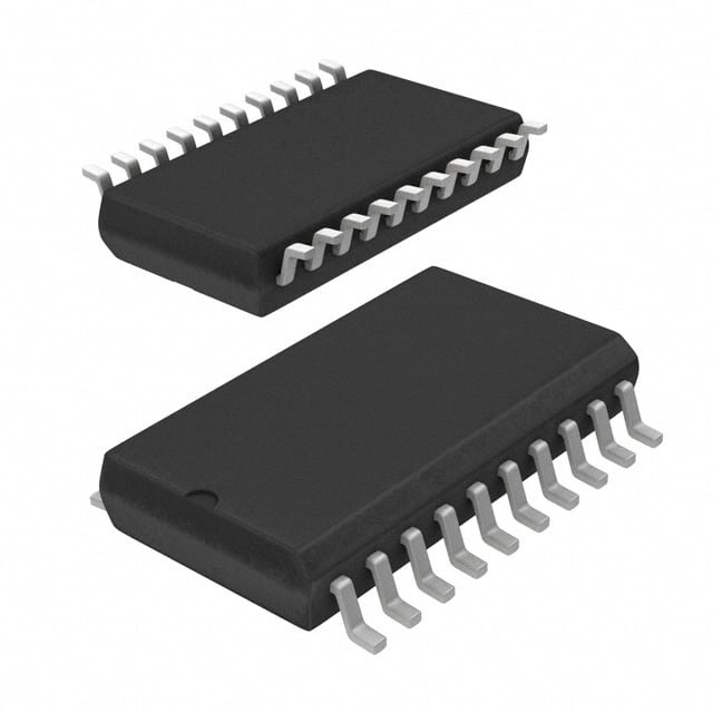
74HCT9115D,112 是恩智浦(NXP USA Inc.)推出的高速CMOS逻辑器件,属于缓冲器/驱动器/收发器类别。该芯片是一款8位双向总线收发器,带三态输出和方向控制(DIR)及输出使能(OE)引脚,采用TSSOP-20封装,兼容74HCT系列电平(输入兼容TTL,输出为CMOS电平,VCC=4.5–5.5V)。

典型应用场景包括:
✅ 微控制器系统总线扩展:在MCU(如ARM Cortex-M或传统8/16位单片机)与外设(如EEPROM、ADC、FPGA配置接口)之间提供双向数据隔离与驱动能力,增强总线负载驱动能力(IOH/IOL达±4mA)。
✅ 板级信号电平缓冲与方向切换:用于隔离不同功能模块间的数字信号(如CPU与协处理器通信),通过DIR引脚动态控制数据流向,避免总线冲突。
✅ 工业控制与嵌入式接口电路:在PLC模块、传感器集线器或通信网关中,实现RS-485/RS-232电平转换芯片前级的数据方向管理与信号整形。
✅ 兼容性升级替代:可直接替换74LS245、74HC245等老旧型号,提升噪声容限与功耗性能(静态电流低,抗干扰强)。

其三态输出特性支持多设备共享同一数据总线,广泛应用于需要灵活数据流向控制的中低速数字系统(工作频率典型值≤36MHz @ VCC=5V),不适用于高速SerDes或高频时钟转发场景。
| 参数 | 数值 |
| 产品目录 | 集成电路 (IC)半导体 |
| 描述 | IC BUFF NINE SCHMT TIG 20SOICW缓冲器和线路驱动器 NINE WIDE TRIG BUF |
| 产品分类 | |
| 品牌 | NXP Semiconductors |
| 产品手册 | |
| 产品图片 |
|
| rohs | 符合RoHS无铅 / 符合限制有害物质指令(RoHS)规范要求 |
| 产品系列 | 逻辑集成电路,缓冲器和线路驱动器,NXP Semiconductors 74HCT9115D,11274HCT |
| 数据手册 | |
| 产品型号 | 74HCT9115D,112 |
| PCN封装 | |
| PCN组件/产地 | |
| 产品培训模块 | http://www.digikey.cn/PTM/IndividualPTM.page?site=cn&lang=zhs&ptm=24983 |
| 产品目录页面 | |
| 产品种类 | 缓冲器和线路驱动器 |
| 传播延迟时间 | 13 ns |
| 低电平输出电流 | 4 mA |
| 供应商器件封装 | 20-SO |
| 元件数 | 9 |
| 其它名称 | 568-2917-5 |
| 包装 | 管件 |
| 商标 | NXP Semiconductors |
| 安装类型 | 表面贴装 |
| 安装风格 | SMD/SMT |
| 封装 | Tube |
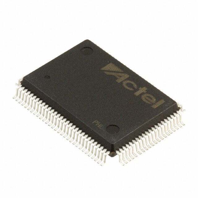
| 封装/外壳 | 20-SOIC(0.295",7.50mm 宽) |
| 封装/箱体 | SOIC-20 |
| 工作温度 | -40°C ~ 125°C |
| 工厂包装数量 | 1520 |
| 最大工作温度 | + 125 C |
| 最小工作温度 | - 40 C |
| 极性 | Non-Inverting |
| 标准包装 | 38 |
| 每元件位数 | 1 |
| 每芯片的通道数量 | 9 |
| 电压-电源 | 4.5 V ~ 5.5 V |
| 电流-输出高,低 | -,4mA |
| 电源电压-最大 | 5.5 V |
| 电源电压-最小 | 4.5 V |
| 输入线路数量 | 9 |
| 输出类型 | Open Drain |
| 输出线路数量 | 9 |
| 逻辑类型 | CMOS |
| 逻辑系列 | HCT |
| 零件号别名 | 74HCT9115D |
| 高电平输出电流 | - 4 mA |


- 商务部:美国ITC正式对集成电路等产品启动337调查
- 曝三星4nm工艺存在良率问题 高通将骁龙8 Gen1或转产台积电
- 太阳诱电将投资9.5亿元在常州建新厂生产MLCC 预计2023年完工
- 英特尔发布欧洲新工厂建设计划 深化IDM 2.0 战略
- 台积电先进制程称霸业界 有大客户加持明年业绩稳了
- 达到5530亿美元!SIA预计今年全球半导体销售额将创下新高
- 英特尔拟将自动驾驶子公司Mobileye上市 估值或超500亿美元
- 三星加码芯片和SET,合并消费电子和移动部门,撤换高东真等 CEO
- 三星电子宣布重大人事变动 还合并消费电子和移动部门
- 海关总署:前11个月进口集成电路产品价值2.52万亿元 增长14.8%


PDF Datasheet 数据手册内容提取
Important notice Dear Customer, On 7 February 2017 the former NXP Standard Product business became a new company with the tradename Nexperia. Nexperia is an industry leading supplier of Discrete, Logic and PowerMOS semiconductors with its focus on the automotive, industrial, computing, consumer and wearable application markets In data sheets and application notes which still contain NXP or Philips Semiconductors references, use the references to Nexperia, as shown below. Instead of http://www.nxp.com, http://www.philips.com/ or http://www.semiconductors.philips.com/, use http://www.nexperia.com Instead of sales.addresses@www.nxp.com or sales.addresses@www.semiconductors.philips.com, use salesaddresses@nexperia.com (email) Replace the copyright notice at the bottom of each page or elsewhere in the document, depending on the version, as shown below: - © NXP N.V. (year). All rights reserved or © Koninklijke Philips Electronics N.V. (year). All rights reserved Should be replaced with: - © Nexperia B.V. (year). All rights reserved. If you have any questions related to the data sheet, please contact our nearest sales office via e-mail or telephone (details via salesaddresses@nexperia.com). Thank you for your cooperation and understanding, Kind regards, Team Nexperia
INTEGRATED CIRCUITS DATA SHEET For a complete data sheet, please also download: •The IC06 74HC/HCT/HCU/HCMOS Logic Family Specifications •The IC06 74HC/HCT/HCU/HCMOS Logic Package Information •The IC06 74HC/HCT/HCU/HCMOS Logic Package Outlines 74HC/HCT9115 Nine wide Schmitt trigger buffer; open drain outputs Product specification December 1990 Supersedes data of March 1988 File under Integrated Circuits, IC06
Philips Semiconductors Product specification Nine wide Schmitt trigger buffer; 74HC/HCT9115 open drain outputs FEATURES The Schmitt trigger action in the data inputs transform slowly changing input signals into sharply defined • Schmitt trigger action on all data inputs jitter-free output signals. • Output capability: standard (open drain) The 74HC/HCT9115 have open-drain N-transistor • I category: MSI CC outputs, which are not clamped by a diode connected to V . In the OFF-state, i.e. when one input is HIGH, the CC GENERAL DESCRIPTION output may be pulled to any voltage between GND and V . This allows the device to be used as a Omax The 74HC/HCT9115 are high-speed Si-gate CMOS LOW-to-HIGH or HIGH-to-LOW level shifter. For digital devices and are pin compatible with low power Schottky operation and OR-tied output applications, these devices TTL (LSTTL). They are specified in compliance with must have a pull-up resistor to establish a logic HIGH level. JEDEC standard no. 7A. The “9115” is identical to the “9114” but has non-inverting The 74HC/HCT9115 are nine wide Schmitt trigger buffer outputs. with open drain outputs and Schmitt trigger inputs. QUICK REFERENCE DATA GND=0 V; T =25(cid:176) C; t =t =6 ns amb r f TYPICAL SYMBOL PARAMETER CONDITIONS UNIT HC HCT t / t propagation delay A to Y C =15 pF; V = 5 V 12 13 ns PHL PLZ n n L CC C input capacitance 3.5 3.5 pF I C power dissipation capacitance per buffer notes 1 and 2 5 5 pF PD Notes 1. C is used to determine the dynamic power dissipation (P inm W): PD D P =C · V 2· f +(cid:229) (C · V 2· f ) where: D PD CC i L CC o f =input frequency in MHz i f =output frequency in MHz o (cid:229) (C · V 2· f )=sum of outputs L CC o C =output load capacitance in pF L V =supply voltage in V CC 2. For HC the condition is V =GND to V I CC For HCT the condition is V =GND to V - 1.5 V I CC ORDERING INFORMATION See“74HC/HCT/HCU/HCMOS Logic Package Information”. December1990 2
Philips Semiconductors Product specification Nine wide Schmitt trigger buffer; 74HC/HCT9115 open drain outputs PIN DESCRIPTION PIN NO. SYMBOL NAME AND FUNCTION 1, 2, 3, 4, 5, 6, 7, 8, 9 A to A data inputs 0 8 10 GND ground (0 V) 19, 18, 17, 16, 15, 14, 13, 12, 11 Y to Y data outputs 0 8 20 V positive supply voltage CC alfpage 1 A0 Y0 19 fpage 1 19 A1 Y1 2 18 2 18 A2 Y2 3 17 3 17 4 A3 Y3 16 4 16 A4 Y4 5 15 5 15 A5 Y5 6 14 6 14 A6 Y6 7 13 7 13 A7 Y7 8 12 8 12 A8 Y8 9 11 9 11 MBA016 MBA013 Fig.1 Pin configuration. Fig.2 Logic diagram. Fig.3 IEC logic diagram. December1990 3
Philips Semiconductors Product specification Nine wide Schmitt trigger buffer; 74HC/HCT9115 open drain outputs handbook, halfpage Yn An GND MBA022 Fig.4 Functional diagram. Fig.5 Logic diagram (one Schmitt trigger). FUNCTION TABLE INPUTS OUTPUTS A Y n n L L H Z Notes 1. H=HIGH voltage level L=LOW voltage level Z=high impedance OFF-state December1990 4
Philips Semiconductors Product specification Nine wide Schmitt trigger buffer; 74HC/HCT9115 open drain outputs DC CHARACTERISTICS FOR 74HC For the DC characteristics see“74HC/HCT/HCU/HCMOS Logic Family Specifications”. Transfer characteristics are given below. Output capability: standard I category: MSI CC TRANSFER CHARACTERISTICS FOR 74HC Voltages are referred to GND (ground=0 V) T ((cid:176) C) TEST CONDITIONS amb 74HC SYMBOL PARAMETER UNIT V +25 - 40to+85 - 40to+125 CC WAVEFORMS (V) min. typ. max. min. max. min. max. VT+ positive-going threshold 0.70 1.13 1.50 0.70 1.50 0.70 1.50 V 2.0 Fig.6 1.75 2.37 3.15 1.75 3.15 1.75 3.15 4.5 2.30 3.11 4.20 2.30 4.20 2.30 4.20 6.0 VT- negative-going threshold 0.30 0.70 1.10 0.30 1.10 0.30 1.10 V 2.0 Fig.6 1.35 1.80 2.40 1.35 2.40 1.35 2.40 4.5 1.80 2.43 3.30 1.80 3.30 1.80 3.30 6.0 VH hysteresis (VT+- VT- ) 0.2 0.43 0.80 0.18 0.80 0.15 0.80 V 2.0 Fig.6 0.4 0.57 1.00 0.40 1.00 0.40 1.00 4.5 0.5 0.68 1.10 0.50 1.10 0.50 1.10 6.0 AC CHARACTERISTICS FOR 74HC GND=0 V; t =t =6 ns; C =50 pF r f L T ((cid:176) C) TEST CONDITIONS amb 74HC SYMBOL PARAMETER UNIT V +25 - 40to+85 - 40to+125 CC WAVEFORMS (V) min. typ. max. min. max. min. max. t / t propagation delay 36 115 140 165 ns 2.0 Fig.7 PHL PLZ A to Y 13 22 28 33 4.5 n n 10 19 24 28 6.0 t output transition time 19 75 95 110 ns 2.0 Fig.7 THL 7 15 19 22 4.5 6 13 16 19 6.0 December1990 5
Philips Semiconductors Product specification Nine wide Schmitt trigger buffer; 74HC/HCT9115 open drain outputs DC CHARACTERISTICS FOR 74HCT For the DC characteristics see“74HC/HCT/HCU/HCMOS Logic Family Specifications”. Transfer characteristics are given below. Output capability: standard I category: MSI CC Note to HCT types The value of additional quiescent supply current (D I ) for a unit load of 1 is given in the family specifications. CC To determineD I per input, multiply this value by the unit load coefficient shown in the table below. CC INPUT UNIT LOAD COEFFICIENT A 0.3 n TRANSFER CHARACTERISTICS FOR 74HCT Voltages are referred to GND (ground=0 V) T ((cid:176) C) TEST CONDITIONS amb 74HCT SYMBOL PARAMETER UNIT V +25 - 40to+85 - 40to+125 CC WAVEFORMS (V) min. typ. max. min. max. min. max. VT+ positive-going threshold 0.9 1.50 2.0 0.9 2.0 0.9 2.0 V 4.5 Fig.6 1.2 1.70 2.1 1.2 2.1 1.2 2.1 5.5 VT- negative-going threshold 0.7 1.06 1.4 0.7 1.4 0.7 1.4 V 4.5 Fig.6 0.8 1.27 1.7 0.8 1.7 0.8 2.7 5.5 VH hysteresis (VT+- VT- ) 0.2 0.44 0.8 0.2 0.8 0.2 0.8 V 4.5 Fig.6 0.2 0.44 0.8 0.2 0.8 0.2 0.8 5.5 AC CHARACTERISTICS FOR 74HCT GND=0 V; t =t =6 ns; C =50 pF r f L T ((cid:176) C) TEST CONDITIONS amb 74HCT SYMBOL PARAMETER UNIT V +25 - 40to+85 - 40to+125 CC WAVEFORMS (V) min. typ. max. min. max. min. max. t / t propagation delay 18 31 39 47 ns 4.5 Fig.7 PHL PLZ A to Y n n t output transition time 7 15 19 22 ns 4.5 Fig.7 THL December1990 6
Philips Semiconductors Product specification Nine wide Schmitt trigger buffer; 74HC/HCT9115 open drain outputs TRANSFER CHARACTERISTIC WAVEFORMS handbook, halfpage VO MBA325 VH VI V V T T Fig.6 Transfer characteristic. AC WAVEFORMS tr tf handbook, full pagewidth 90 % An INPUT VM(1) 10 % tPLZ tPZL Yn OUTPUT 10 % t MBA023 THL (1) HC : VM=50%; VI=GND to VCC. HCT: VM=1.3 V; VI=GND to 3 V. Fig.7 Waveforms showing the input (A ) to output (Y ) propagation delays and the output transition times. n n PACKAGE OUTLINES See“74HC/HCT/HCU/HCMOS Logic Package Outlines”. December1990 7