ICGOO在线商城 > 隔离器 > 光隔离器 - 晶体管,光电输出 > PS2561AL1-1-L-A
 Datasheet下载
- 型号: PS2561AL1-1-L-A
- 制造商: CEL
- 库位|库存: xxxx|xxxx
- 要求:
| 数量阶梯 | 香港交货 | 国内含税 |
| +xxxx | $xxxx | ¥xxxx |
查看当月历史价格
查看今年历史价格
PS2561AL1-1-L-A产品简介:
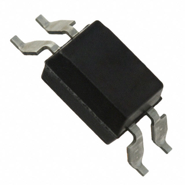
ICGOO电子元器件商城为您提供PS2561AL1-1-L-A由CEL设计生产,在icgoo商城现货销售,并且可以通过原厂、代理商等渠道进行代购。 PS2561AL1-1-L-A价格参考。CELPS2561AL1-1-L-A封装/规格:光隔离器 - 晶体管,光电输出, 光隔离器 晶体管 输出 5000Vrms 1 通道 4-DIP。您可以下载PS2561AL1-1-L-A参考资料、Datasheet数据手册功能说明书,资料中有PS2561AL1-1-L-A 详细功能的应用电路图电压和使用方法及教程。
CEL品牌的PS2561AL1-1-L-A光隔离器属于晶体管类型,具有光电输出功能。该型号主要用于需要电气隔离和信号传输的场合,具体应用场景如下:

1. 工业自动化与控制:
   - 在工业控制系统中,用于隔离传感器、执行器和其他电子设备之间的信号传输,防止干扰和噪声对系统稳定性的影响。
   - 适用于PLC(可编程逻辑控制器)、DCS(分布式控制系统)等设备中的信号隔离。

2. 电力系统保护:
   - 用于电力监控和保护装置中,实现高低压侧的电气隔离,确保安全性和可靠性。
   - 应用于断路器、继电器等设备的信号传输部分,防止高压侧对低压控制电路的干扰。

3. 通信设备:
   - 在通信基站、路由器、交换机等设备中,用于隔离不同电位的信号线路,提高通信系统的抗干扰能力。
   - 适用于光纤通信系统中的光电转换模块,确保信号的稳定传输。

4. 医疗设备:
   - 在医疗仪器中,如心电图机、监护仪等,用于隔离患者与设备之间的电气连接,确保患者安全。
   - 提供可靠的信号传输通道,避免外界电磁干扰影响测量精度。

5. 汽车电子:
   - 用于汽车电子控制系统中,如发动机控制单元(ECU)、车身控制系统等,实现传感器与控制单元之间的电气隔离。
   - 提高汽车电子系统的抗干扰能力和安全性,确保各子系统的正常工作。

6. 消费电子产品:
   - 在家用电器、智能穿戴设备等产品中,用于隔离电源和信号线路,防止电源波动对敏感电路的影响。
   - 提升产品的可靠性和用户体验,延长使用寿命。

总之,PS2561AL1-1-L-A光隔离器广泛应用于各种需要电气隔离和信号传输的场合,能够有效提高系统的抗干扰能力和安全性,确保信号的稳定传输。
| 参数 | 数值 |
| 产品目录 | |
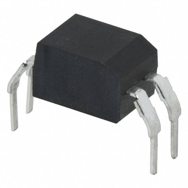
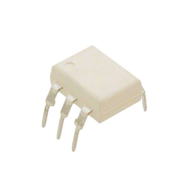
| 描述 | OPTOISOLATOR 5KV TRANS 4DIP晶体管输出光电耦合器 BV= 5000Vr.m.s. Creep 7mm Min. |
| 产品分类 | |
| 品牌 | CEL |
| 产品手册 | |
| 产品图片 |
|
| rohs | 符合RoHS无铅 / 符合限制有害物质指令(RoHS)规范要求 |
| 产品系列 | 光耦合器/光电耦合器,晶体管输出光电耦合器,CEL PS2561AL1-1-L-ANEPOC |
| 数据手册 | |
| 产品型号 | PS2561AL1-1-L-A |
| Vce饱和值(最大值) | 300mV |
| 上升/下降时间(典型值) | 3µs, 5µs |
| 产品培训模块 | http://www.digikey.cn/PTM/IndividualPTM.page?site=cn&lang=zhs&ptm=22067 |
| 产品目录页面 | |
| 产品种类 | Optocouplers |
| 供应商器件封装 | 4-DIP |
| 其它名称 | PS2561AL11LA |
| 其它图纸 |
|
| 包装 | 管件 |
| 商标 | CEL |
| 安装类型 | 通孔 |
| 封装 | Tube |
| 封装/外壳 | 4-DIP(0.400",10.16mm) |
| 封装/箱体 | DIP-4 |
| 工作温度 | -55°C ~ 100°C |
| 工厂包装数量 | 100 |
| 打开/关闭时间(典型值) | - |
| 最大上升时间 | 3 us |
| 最大下降时间 | 5 us |
| 最大功率耗散 | 150 mW |
| 最大反向二极管电压 | 6 V |
| 最大工作温度 | + 100 C |
| 最大正向二极管电压 | 1.4 V |
| 最大集电极/发射极电压 | 70 V |
| 最大集电极/发射极饱和电压 | 0.3 V |
| 最大集电极电流 | 30 mA |
| 最小工作温度 | - 55 C |
| 标准包装 | 100 |
| 正向电流 | 10 mA |
| 每芯片的通道数量 | 1 Channel |
| 电压-正向(Vf)(典型值) | 1.2V |
| 电压-输出(最大值) | 70V |
| 电压-隔离 | 5000Vrms |
| 电流-DC正向(If) | 30mA |
| 电流-输出/通道 | 30mA |
| 电流传输比(最大值) | 400% @ 5mA |
| 电流传输比(最小值) | 200% @ 5mA |
| 电流传递比 | 50 % to 400 % |
| 绝缘电压 | 5000 Vrms |
| 输入类型 | DC |
| 输出类型 | 晶体管 |
| 输出设备 | NPN Phototransistor |
| 通道数 | 1 |


.jpg)


- 商务部:美国ITC正式对集成电路等产品启动337调查
- 曝三星4nm工艺存在良率问题 高通将骁龙8 Gen1或转产台积电
- 太阳诱电将投资9.5亿元在常州建新厂生产MLCC 预计2023年完工
- 英特尔发布欧洲新工厂建设计划 深化IDM 2.0 战略
- 台积电先进制程称霸业界 有大客户加持明年业绩稳了
- 达到5530亿美元!SIA预计今年全球半导体销售额将创下新高
- 英特尔拟将自动驾驶子公司Mobileye上市 估值或超500亿美元
- 三星加码芯片和SET,合并消费电子和移动部门,撤换高东真等 CEO
- 三星电子宣布重大人事变动 还合并消费电子和移动部门
- 海关总署:前11个月进口集成电路产品价值2.52万亿元 增长14.8%
.jpg)

(B)(TU)-VG.jpg)
PDF Datasheet 数据手册内容提取
PHOTOCOUPLER PS2561A-1,PS2561AL-1,PS2561AL1-1,PS2561AL2-1 HIGH ISOLATION VOLTAGE SINGLE TRANSISTOR TYPE NEPOC Series MULTI PHOTOCOUPLER SERIES DESCRIPTION The PS2561A-1 is an optically coupled isolator containing a GaAs light emitting diode and an NPN silicon phototransistor to realize an excellent cost performance. The PS2561A-1 is in a plastic DIP (Dual In-line Package) and the PS2561AL-1 is lead bending type (Gull-wing) for surface mount. The PS2561AL1-1 is lead bending L1 type and the PS2561AL2-1 is lead bending L2 type (Gull-wing). FEATURES • High isolation voltage (BV = 5 000 Vr.m.s.) <R> • Ordering number of taping product: PS2561AL-1-F3 : 2 000 pcs/reel : PS2561AL2-1-E3: 1 000 pcs/reel • Pb-Free product <R> • Safety standards • UL approved: No. E72422 • CSA approved: No. CA 101391 (CA5A, CAN/CSA-C22.2 60065, 60950) • BSI approved: No. 7112/7420 • SEMKO approved: No. 903238 • NEMKO approved: No. P09210868 • DEMKO approved: No. 314999 • FIMKO approved: No. FI 25119 • DIN EN60747-5-2 (VDE0884 Part2) approved: No. 40008862 (Option) APPLICATIONS • Power supply • Telephone/FAX. • FA/OA equipment • Programmable logic controller Document No. PN10222EJ08V0DS (8th edition) Date Published September 2009 NS The mark <R> shows major revised points. The revised points can be easily searched by copying an "<R>" in the PDF file and specifying it in the "Find what:" field.
PS2561A-1,PS2561AL-1,PS2561AL1-1,PS2561AL2-1 PACKAGE DIMENSIONS (UNIT : mm) DIP Type Long Creepage Distance Lead Bending Type (Gull-Wing) Long Creepage Distance (Gull-Wing) PHOTOCOUPLER CONSTRUCTION Parameter Unit (MIN.) Air Distance 7 mm Outer Creepage Distance 7 mm Inner Creepage Distance 4 mm Isolation Thickness 0.4 mm 2 Data Sheet PN10222EJ08V0DS
PS2561A-1,PS2561AL-1,PS2561AL1-1,PS2561AL2-1 MARKING EXAMPLE Data Sheet PN10222EJ08V0DS 3
PS2561A-1,PS2561AL-1,PS2561AL1-1,PS2561AL2-1 <R> ORDERING INFORMATION Part Number Order Number Solder Plating Packing Style Safety Standard Application Part Specification Approval Number *1 PS2561A-1 PS2561A-1-A Pb-Free Magazine case 100 pcs Standard products PS2561A-1 PS2561AL-1 PS2561AL-1-A (UL, CSA, BSI, PS2561AL1-1 PS2561AL1-1-A SEMKO, NEMKO, PS2561AL2-1 PS2561AL2-1-A DEMKO, FIMKO PS2561AL-1-F3 PS2561AL-1-F3-A Embossed Tape 2 000 pcs/reel approved) PS2561AL2-1-E3 PS2561AL2-1-E3-A Embossed Tape 1 000 pcs/reel PS2561A-1-V PS2561A-1-V-A Magazine case 100 pcs DIN EN60747-5-2 PS2561AL-1-V PS2561AL-1-V-A (VDE0884 Part2) PS2561AL1-1-V PS2561AL1-1-V-A Approved (option) PS2561AL2-1-V PS2561AL2-1-V-A PS2561AL-1-V-F3 PS2561AL-1-V-F3-A Embossed Tape 2 000 pcs/reel PS2561AL2-1-V-E3 PS2561AL2-1-V-E3-A Embossed Tape 1 000 pcs/reel PS2561A-1 PS2561A-1Y-A Special version Magazine case 100 pcs Standard products PS2561A-1 PS2561AL-1 PS2561AL-1Y-A (Pb-Free and (UL, CSA, BSI, PS2561AL1-1 PS2561AL1-1Y-A Halogen Free) SEMKO, NEMKO, PS2561AL2-1 PS2561AL2-1Y-A DEMKO, FIMKO PS2561AL-1-F3 PS2561AL-1Y-F3-A Embossed Tape 2 000 pcs/reel approved) PS2561AL2-1-E3 PS2561AL2-1Y-E3-A Embossed Tape 1 000 pcs/reel PS2561A-1-V PS2561A-1Y-V-A Magazine case 100 pcs DIN EN60747-5-2 PS2561AL-1-V PS2561AL-1Y-V-A (VDE0884 Part2) PS2561AL1-1-V PS2561AL1-1Y-V-A Approved (option) PS2561AL2-1-V PS2561AL2-1Y-V-A PS2561AL-1-V-F3 PS2561AL-1Y-V-F3-A Embossed Tape 2 000 pcs/reel PS2561AL2-1-V-E3 PS2561AL2-1Y-V-E3-A Embossed Tape 1 000 pcs/reel *1 For the application of the Safety Standard, following part number should be used. 4 Data Sheet PN10222EJ08V0DS
PS2561A-1,PS2561AL-1,PS2561AL1-1,PS2561AL2-1 ABSOLUTE MAXIMUM RATINGS (TA = 25 C, unless otherwise specified) Parameter Symbol Ratings Unit Diode Reverse Voltage VR 6 V Forward Current (DC) IF 30 mA Power Dissipation Derating PD/ C 1.5 mW/ C Power Dissipation PD 150 mW Peak Forward Current*1 IFP 0.5 A Transistor Collector to Emitter Voltage VCEO 70 V Emitter to Collector Voltage VECO 5 V Collector Current IC 30 mA Power Dissipation Delay PC/ C 1.5 mW/ C Power Dissipation PC 150 mW Isolation Voltage*2 BV 5 000 Vr.m.s. Operating Ambient Temperature TA 55 to +100 C Storage Temperature Tstg 55 to +150 C *1 PW = 100 s, Duty Cycle = 1% *2 AC voltage for 1 minute at TA = 25 C, RH = 60% between input and output. Pins 1-2 shorted together, 3-4 shorted together. Data Sheet PN10222EJ08V0DS 5
PS2561A-1,PS2561AL-1,PS2561AL1-1,PS2561AL2-1 ELECTRICAL CHARACTERISTICS (TA = 25 C) Parameter Symbol Conditions MIN. TYP. MAX. Unit Diode Forward Voltage VF IF = 10 mA 1.2 1.4 V Reverse Current IR VR = 5 V 5 A Terminal Capacitance Ct V = 0 V, f = 1.0 MHz 10 pF Transistor Collector to Emitter Dark ICEO VCE = 70 V, IF = 0 mA 100 nA Current Coupled Current Transfer Ratio CTR IF = 5 mA, VCE = 5 V 50 400 % (IC/IF)*1 Collector Saturation VCE (sat) IF = 10 mA, IC = 2 mA 0.13 0.3 V Voltage Isolation Resistance RI-O VI-O = 1.0 kVDC 1011 Isolation Capacitance CI-O V = 0 V, f = 1.0 MHz 0.4 pF Rise Time*2 tr VCC = 10 V, IC = 2 mA, RL = 100 3 s Fall Time*2 tf 5 *1 CTR rank N : 50 to 400 (%) H : 80 to 160 (%) Q : 100 to 200 (%) W : 130 to 260 (%) L : 200 to 400 (%) *2 Test circuit for switching time 6 Data Sheet PN10222EJ08V0DS
PS2561A-1,PS2561AL-1,PS2561AL1-1,PS2561AL2-1 TYPICAL CHARACTERISTICS (TA = 25 C, unless otherwise specified) Remark The graphs indicate nominal characteristics. Data Sheet PN10222EJ08V0DS 7
PS2561A-1,PS2561AL-1,PS2561AL1-1,PS2561AL2-1 Remark The graphs indicate nominal characteristics. 8 Data Sheet PN10222EJ08V0DS
PS2561A-1,PS2561AL-1,PS2561AL1-1,PS2561AL2-1 <R> TAPING SPECIFICATIONS (UNIT : mm) Data Sheet PN10222EJ08V0DS 9
PS2561A-1,PS2561AL-1,PS2561AL1-1,PS2561AL2-1 10 Data Sheet PN10222EJ08V0DS
PS2561A-1,PS2561AL-1,PS2561AL1-1,PS2561AL2-1 NOTES ON HANDLING 1. Recommended soldering conditions (1) Infrared reflow soldering • Peak reflow temperature 260 C or below (package surface temperature) • Time of peak reflow temperature 10 seconds or less • Time of temperature higher than 220 C 60 seconds or less • Time to preheat temperature from 120 to 180 C 120 30 s • Number of reflows Three • Flux Rosin flux containing small amount of chlorine (The flux with a maximum chlorine content of 0.2 Wt% is recommended.) (2) Wave soldering • Temperature 260 C or below (molten solder temperature) • Time 10 seconds or less • Preheating conditions 120 C or below (package surface temperature) • Number of times One (Allowed to be dipped in solder including plastic mold portion.) • Flux Rosin flux containing small amount of chlorine (The flux with a maximum chlorine content of 0.2 Wt% is recommended.) (3) Soldering by soldering iron • Peak temperature (lead part temperature) 350 C or below • Time (each pins) 3 seconds or less • Flux Rosin flux containing small amount of chlorine (The flux with a maximum chlorine content of 0.2 Wt% is recommended.) (a) Soldering of leads should be made at the point 1.5 to 2.0 mm from the root of the lead. (b) Please be sure that the temperature of the package would not be heated over 100 C. Data Sheet PN10222EJ08V0DS 11
PS2561A-1,PS2561AL-1,PS2561AL1-1,PS2561AL2-1 (4) Cautions • Fluxes Avoid removing the residual flux with freon-based and chlorine-based cleaning solvent. 2. Cautions regarding noise Be aware that when voltage is applied suddenly between the photocoupler’s input and output or between collector-emitters at startup, the output transistor may enter the on state, even if the voltage is within the absolute maximum ratings. 3. Measurement conditions of current transfer ratios (CTR), which differ according to photocoupler Check the setting values before use, since the forward current conditions at CTR measurement differ according to product. When using products other than at the specified forward current, the characteristics curves may differ from the standard curves due to CTR value variations or the like. This tendency may sometimes be obvious, especially below IF = 1 mA. Therefore, check the characteristics under the actual operating conditions and thoroughly take variations or the like into consideration before use. USAGE CAUTIONS 1. Protect against static electricity when handling. 2. Avoid storage at a high temperature and high humidity. 12 Data Sheet PN10222EJ08V0DS
PS2561A-1,PS2561AL-1,PS2561AL1-1,PS2561AL2-1 SPECIFICATION OF VDE MARKS LICENSE DOCUMENT Parameter Symbol Spec. Unit Climatic test class (IEC 60068-1/DIN EN 60068-1) 55/100/21 Dielectric strength maximum operating isolation voltage UIORM 890 Vpeak Test voltage (partial discharge test, procedure a for type test and random test) Upr 1 335 Vpeak Upr = 1.5 UIORM, Pd 5 pC Test voltage (partial discharge test, procedure b for all devices) Upr 1 669 Vpeak Upr = 1.875 UIORM, Pd 5 pC Highest permissible overvoltage UTR 8 000 Vpeak Degree of pollution (DIN EN 60664-1 VDE0110 Part 1) 2 Comparative tracking index (IEC 60112/DIN EN 60112 (VDE 0303 Part 11)) CTI 175 Material group (DIN EN 60664-1 VDE0110 Part 1) III a Storage temperature range Tstg –55 to +150 C Operating temperature range TA –55 to +100 C Isolation resistance, minimum value VIO = 500 V dc at TA = 25 C Ris MIN. 1012 VIO = 500 V dc at TA MAX. at least 100 C Ris MIN. 1011 Safety maximum ratings (maximum permissible in case of fault, see thermal derating curve) Package temperature Tsi 175 C Current (input current IF, Psi = 0) Isi 400 mA Power (output or total power dissipation) Psi 700 mW Isolation resistance VIO = 500 V dc at TA = Tsi Ris MIN. 109 Data Sheet PN10222EJ08V0DS 13
PS2561A-1,PS2561AL-1,PS2561AL1-1,PS2561AL2-1 14 Data Sheet PN10222EJ08V0DS
PS2561A-1,PS2561AL-1,PS2561AL1-1,PS2561AL2-1 This product uses gallium arsenide (GaAs). Caution GaAs Products GaAs vapor and powder are hazardous to human health if inhaled or ingested, so please observe the following points. • Follow related laws and ordinances when disposing of the product. If there are no applicable laws and/or ordinances, dispose of the product as recommended below. 1. Commission a disposal company able to (with a license to) collect, transport and dispose of materials that contain arsenic and other such industrial waste materials. 2. Exclude the product from general industrial waste and household garbage, and ensure that the product is controlled (as industrial waste subject to special control) up until final disposal. • Do not burn, destroy, cut, crush, or chemically dissolve the product. • Do not lick the product or in any way allow it to enter the mouth.
Mouser Electronics Authorized Distributor Click to View Pricing, Inventory, Delivery & Lifecycle Information: C EL: PS2561AL-1-H-A PS2561A-1-F3-A PS2561A-1-A PS2561A-1-W-A PS2561AL-1-N-A PS2561AL-1-V-A PS2561AL-1-W-A PS2561AL1-1-V-A PS2561AL1-1-V-D-A PS2561AL2-1-E3-L-A PS2561AL-1-F3-L-A PS2561AL1- 1-L-A PS2561AL2-1-E3-H-A PS2561AL2-1-H-A PS2561AL2-1-V-E3-L-A PS2561A-1-V-H-A PS2561A-1-V-L-A PS2561AL1-1-V-W-A PS2561AL2-1-V-H-A PS2561AL2-1-V-W-A PS2561AL-1-V-F3-L-A PS2561A-1-H-A PS2561A- 1-H-V-A PS2561A-1-V-A PS2561AL-1-A PS2561AL-1-F3-A PS2561AL-1-Q-A PS2561AL-1-V-H-A PS2561AL1-1- F3-H-A PS2561AL1-1-H-A PS2561AL2-1-A PS2561AL2-1-V-A PS2561AL1-1-A PS2561AL-1-F3-H-A PS2561AL-1- F3-Q-A PS2561AL-1-F3-W-A PS2561AL-1-V-F3-A PS2561AL2-1-E3-Q-A PS2561AL2-1-Q-A