ICGOO在线商城 > 隔离器 > 光隔离器 - 晶体管,光电输出 > H11F1TVM

 Datasheet下载
- 型号: H11F1TVM
- 制造商: Fairchild Semiconductor
- 库位|库存: xxxx|xxxx
- 要求:
| 数量阶梯 | 香港交货 | 国内含税 |
| +xxxx | $xxxx | ¥xxxx |
查看当月历史价格
查看今年历史价格
H11F1TVM产品简介:
ICGOO电子元器件商城为您提供H11F1TVM由Fairchild Semiconductor设计生产,在icgoo商城现货销售,并且可以通过原厂、代理商等渠道进行代购。 H11F1TVM价格参考¥10.16-¥10.16。Fairchild SemiconductorH11F1TVM封装/规格:光隔离器 - 晶体管,光电输出, 光隔离器 MOSFET 输出 7500Vpk 1 通道 6-DIP。您可以下载H11F1TVM参考资料、Datasheet数据手册功能说明书,资料中有H11F1TVM 详细功能的应用电路图电压和使用方法及教程。
ON Semiconductor的H11F1TVM是一款光隔离器,属于光电晶体管输出类型。其主要应用场景包括以下几方面:

1. 工业控制:H11F1TVM可用于工业自动化设备中的信号隔离,例如可编程逻辑控制器(PLC)、传感器接口和电机驱动电路。它能够有效防止噪声干扰,确保控制信号的稳定传输。

2. 电源管理:在开关电源、逆变器和不间断电源(UPS)系统中,该器件可用于实现初级和次级电路之间的电气隔离,保护敏感电路免受高压影响。

3. 通信设备:在通信系统中,H11F1TVM可以用于隔离输入/输出信号,避免地环路问题,提高系统的抗干扰能力。

4. 医疗设备:在医疗电子领域,如心电图机、血压监测仪等设备中,该光隔离器可用于患者与设备之间的安全隔离,确保符合相关医疗安全标准。

5. 汽车电子:在汽车电子控制系统中,H11F1TVM可用于信号隔离,例如发动机控制单元(ECU)、车身控制系统等,以提高系统的可靠性和安全性。

6. 家用电器:在家电产品中,如洗衣机、空调和微波炉等,该器件可用于隔离主控板与功率驱动电路之间的信号,增强系统的稳定性。

H11F1TVM通过光耦合技术实现输入和输出之间的电气隔离,具有高可靠性、长寿命和良好的抗电磁干扰能力,适用于需要高隔离电压和低功耗的应用场合。
| 参数 | 数值 |
| 产品目录 | |
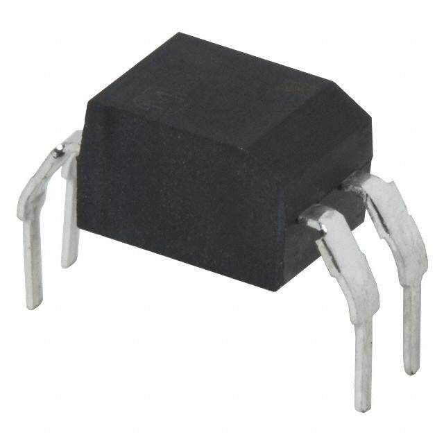
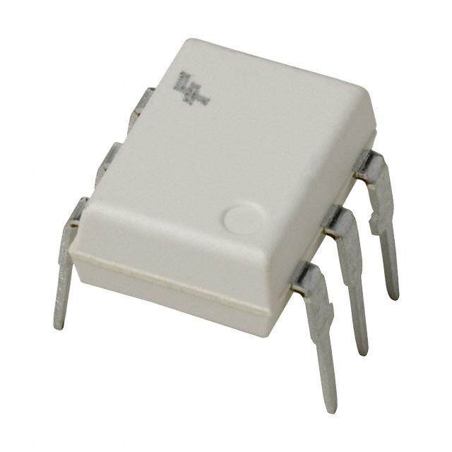
| 描述 | OPTOISOLTR 7.5KV PHOTO FET 6-DIP |
| 产品分类 | |
| 品牌 | Fairchild Semiconductor |
| 数据手册 | |
| 产品图片 |
|
| 产品型号 | H11F1TVM |
| rohs | 无铅 / 符合限制有害物质指令(RoHS)规范要求 |
| 产品系列 | - |
| Vce饱和值(最大值) | - |
| 上升/下降时间(典型值) | - |
| 产品目录页面 | |
| 供应商器件封装 | 6-DIP |
| 包装 | 管件 |
| 安装类型 | 通孔 |
| 封装/外壳 | 6-DIP(0.300",7.62mm) |
| 工作温度 | -40°C ~ 100°C |
| 打开/关闭时间(典型值) | 45µs, 45µs (最小值) |
| 标准包装 | 1,000 |
| 电压-正向(Vf)(典型值) | 1.3V |
| 电压-输出(最大值) | 30V |
| 电压-隔离 | 7500Vpk |
| 电流-DC正向(If) | 60mA |
| 电流-输出/通道 | - |
| 电流传输比(最大值) | - |
| 电流传输比(最小值) | - |
| 输入类型 | DC |
| 输出类型 | 光电 FET |
| 通道数 | 1 |


.jpg)

(B)(TU)-VG.jpg)

- 商务部:美国ITC正式对集成电路等产品启动337调查
- 曝三星4nm工艺存在良率问题 高通将骁龙8 Gen1或转产台积电
- 太阳诱电将投资9.5亿元在常州建新厂生产MLCC 预计2023年完工
- 英特尔发布欧洲新工厂建设计划 深化IDM 2.0 战略
- 台积电先进制程称霸业界 有大客户加持明年业绩稳了
- 达到5530亿美元!SIA预计今年全球半导体销售额将创下新高
- 英特尔拟将自动驾驶子公司Mobileye上市 估值或超500亿美元
- 三星加码芯片和SET,合并消费电子和移动部门,撤换高东真等 CEO
- 三星电子宣布重大人事变动 还合并消费电子和移动部门
- 海关总署:前11个月进口集成电路产品价值2.52万亿元 增长14.8%

.jpg)

.jpg)
PDF Datasheet 数据手册内容提取
Is Now Part of To learn more about ON Semiconductor, please visit our website at www.onsemi.com Please note: As part of the Fairchild Semiconductor integration, some of the Fairchild orderable part numbers will need to change in order to meet ON Semiconductor’s system requirements. Since the ON Semiconductor product management systems do not have the ability to manage part nomenclature that utilizes an underscore (_), the underscore (_) in the Fairchild part numbers will be changed to a dash (-). This document may contain device numbers with an underscore (_). Please check the ON Semiconductor website to verify the updated device numbers. The most current and up-to-date ordering information can be found at www.onsemi.com. Please email any questions regarding the system integration to Fairchild_questions@onsemi.com. ON Semiconductor and the ON Semiconductor logo are trademarks of Semiconductor Components Industries, LLC dba ON Semiconductor or its subsidiaries in the United States and/or other countries. ON Semiconductor owns the rights to a number of patents, trademarks, copyrights, trade secrets, and other intellectual property. A listing of ON Semiconductor’s product/patent coverage may be accessed at www.onsemi.com/site/pdf/Patent-Marking.pdf. ON Semiconductor reserves the right to make changes without further notice to any products herein. ON Semiconductor makes no warranty, representation or guarantee regarding the suitability of its products for any particular purpose, nor does ON Semiconductor assume any liability arising out of the application or use of any product or circuit, and specifically disclaims any and all liability, including without limitation special, consequential or incidental damages. Buyer is responsible for its products and applications using ON Semiconductor products, including compliance with all laws, regulations and safety requirements or standards, regardless of any support or applications information provided by ON Semiconductor. “Typical” parameters which may be provided in ON Semiconductor data sheets and/or specifications can and do vary in different applications and actual performance may vary over time. All operating parameters, including “Typicals” must be validated for each customer application by customer’s technical experts. ON Semiconductor does not convey any license under its patent rights nor the rights of others. ON Semiconductor products are not designed, intended, or authorized for use as a critical component in life support systems or any FDA Class 3 medical devices or medical devices with a same or similar classification in a foreign jurisdiction or any devices intended for implantation in the human body. Should Buyer purchase or use ON Semiconductor products for any such unintended or unauthorized application, Buyer shall indemnify and hold ON Semiconductor and its officers, employees, subsidiaries, affiliates, and distributors harmless against all claims, costs, damages, and expenses, and reasonable attorney fees arising out of, directly or indirectly, any claim of personal injury or death associated with such unintended or unauthorized use, even if such claim alleges that ON Semiconductor was negligent regarding the design or manufacture of the part. ON Semiconductor is an Equal Opportunity/Affirmative Action Employer. This literature is subject to all applicable copyright laws and is not for resale in any manner.
H 1 1 F May 2012 1 M , H 1 1 H11F1M, H11F2M, H11F3M F 2 M Photo FET Optocouplers , H 1 1 Features General Description F 3 M As a remote variable resistor: The H11FXM series consists of a Gallium-Aluminum- ■ ≤ 100Ω to ≥ 300MΩ Arsenide IRED emitting diode coupled to a symmetrical — ■ ≤ 15pF shunt capacitance bilateral silicon photo-detector. The detector is electri- P ■ ≥ 100GΩ I/O isolation resistance cally isolated from the input and performs like an ideal h o isolated FET designed for distortion-free control of low t As an analog switch: level AC and DC analog signals. The H11FXM series o ■ Extremely low offset voltage devices are mounted in dual in-line packages. F E ■ 60 Vpk-pk signal capability T ■ No charge injection or latch-up O p ■ UL recognized (File #E90700) t o c Applications o u p As a remote variable resistor: l ■ Isolated variable attenuator e r s ■ Automatic gain control ■ Active filter fine tuning/band switching As an analog switch: ■ Isolated sample and hold circuit ■ Multiplexed, optically isolated A/D conversion Schematic Package Outlines OUTPUT ANODE 1 6 TERM. CATHODE 2 5 OUTPUT 3 4 TERM. ©2007 Fairchild Semiconductor Corporation www.fairchildsemi.com H11F1M, H11F2M, H11F3M Rev. 1.0.5
H 1 Absolute Maximum Ratings (T = 25°C unless otherwise specified) 1 A F Stresses exceeding the absolute maximum ratings may damage the device. The device may not function or be 1 M operable above the recommended operating conditions and stressing the parts to these levels is not recommended. , In addition, extended exposure to stresses above the recommended operating conditions may affect device reliability. H The absolute maximum ratings are stress ratings only. 1 1 F Symbol Parameter Device Value Units 2M TOTAL DEVICE , H 1 T Storage Temperature All -40 to +150 °C STG 1 F TOPR Operating Temperature All -40 to +100 °C 3 M T Lead Solder Temperature All 260 for 10 sec °C SOL — EMITTER P I Continuous Forward Current All 60 mA h F o V Reverse Voltage All 5 V t R o I Forward Current – Peak (10µs pulse, 1% duty cycle) All 1 A F F(pk) E P LED Power Dissipation 25°C Ambient All 100 mW T D O Derate Linearly from 25°C 1.33 mW/°C p DETECTOR to c P Detector Power Dissipation @ 25°C All 300 mW o D u Derate linearly from 25°C 4.0 mW/°C p l e BV4-6 Breakdown Voltage (either polarity) H11F1M, ±30 V r s H11F2M H11F3M ±15 V I Continuous Detector Current (either polarity) All ±100 mA 4-6 ©2007 Fairchild Semiconductor Corporation www.fairchildsemi.com H11F1M, H11F2M, H11F3M Rev. 1.0.5 2
H 1 Electrical Characteristics (TA = 25°C unless otherwise specified.) 1F 1 Individual Component Characteristics M , Symbol Parameter Test Conditions Device Min. Typ.* Max. Unit H 1 EMITTER 1 F V Input Forward Voltage I = 16mA All 1.3 1.75 V 2 F F M IR Reverse Leakage Current VR = 5V All 10 µA , H C Capacitance V = 0 V, f = 1.0MHz All 50 pF 1 J 1 F OUTPUT DETECTOR 3 M BV Breakdown Voltage I = 10µA, I = 0 H11F1M, H11F2M 30 V 4-6 4-6 F Either Polarity — H11F3M 15 P I4-6 Off-State Dark Current V4-6 = 15 V, IF = 0 All 50 nA h o V4-6 = 15 V, IF = 0, All 50 µA to TA = 100°C F R Off-State Resistance V = 15 V, I = 0 All 300 MΩ E 4-6 4-6 F T C4-6 Capacitance V4-6 = 15 V, IF = 0, All 15 pF O f = 1MHz p t o c Transfer Characteristics o u p Symbol Characteristics Test Conditions Device Min Typ* Max Units l e DC CHARACTERISTICS rs R On-State Resistance I = 16mA, H11F1M 200 Ω 4-6 F I = 100µA 4-6 H11F2M 330 H11F3M 470 R On-State Resistance I = 16mA, H11F1M 200 Ω 6-4 F I = 100µA 6-4 H11F2M 330 H11F3M 470 Resistance, non-linearity I = 16mA, All 2 % F and assymetry I = 25µA RMS, 4-6 f = 1kHz AC CHARACTERISTICS t Turn-On Time R = 50Ω, I = 16mA, All 45 µs on L F V = 5V 4-6 t Turn-Off Time R = 50Ω, I = 16mA, All 45 µs off L F V = 5V 4-6 Isolation Characteristics Symbol Characteristic Test Conditions Device Min. Typ.* Max. Units V Isolation Voltage f = 60Hz, t = 1 sec. All 7500 V PEAK ISO AC R Isolation Resistance V = 500 VDC All 1011 Ω ISO I-O C Isolation Capacitance f = 1MHz All 0.2 pF ISO *All Typical values at T = 25°C A ©2007 Fairchild Semiconductor Corporation www.fairchildsemi.com H11F1M, H11F2M, H11F3M Rev. 1.0.5 3
H 1 Safety and Insulation Ratings 1 F 1 As per IEC 60747-5-2, this optocoupler is suitable for “safe electrical insulation” only within the safety limit data. M Compliance with the safety ratings shall be ensured by means of protective circuits. , H Symbol Parameter Min. Typ. Max. Unit 1 1 F Installation Classifications per DIN VDE 0110/1.89 2 Table 1 M , For Rated Main Voltage < 150Vrms I-IV H 1 For Rated Main voltage < 300Vrms I-IV 1 F Climatic Classification 55/100/21 3 M Pollution Degree (DIN VDE 0110/1.89) 2 — CTI Comparative Tracking Index 175 P V Input to Output Test Voltage, Method b, V x 1.875 1594 V h PR IORM peak o = VPR, 100% Production Test with tm = 1 sec, Partial to Discharge < 5pC F E Input to Output Test Voltage, Method a, V x 1.5 = 1275 V IORM peak T VPR, Type and Sample Test with tm = 60 sec, Partial O Discharge < 5pC p t V Max. Working Insulation Voltage 850 V o IORM peak c V Highest Allowable Over Voltage 6000 V o IOTM peak u External Creepage 7 mm p l e External Clearance 7 mm r s Insulation Thickness 0.5 mm RIO Insulation Resistance at Ts, V = 500V 109 Ω IO ©2007 Fairchild Semiconductor Corporation www.fairchildsemi.com H11F1M, H11F2M, H11F3M Rev. 1.0.5 4
H 1 Typical Performance Curves 1 F 1 M Figure 1. Resistance vs. Input Current Figure 2. Output Characteristics , H 800 1 IF = 18mA 1 F 600 IF = 14mA 2 ED RESISTANCE 10 μCURRENT (A) 4200000 IF = 2mA IIIFFF === 1620mmmAAA M, H11F3 RMALIZ 1 UTPUT -200 IF = 6mA M — O O IF = 10mA n) – N I – 46 -400 IF = 14mA Ph r(o Normalized to: -600 IF = 18mA ot o IIF46 = = 1 56μmAA RMS -800 F 0.1 E 1 1 0 100 -0.2 -0.1 0.0 0.1 0.2 T IF – INPUT CURRENT (mA) V46 – OUTPUT VOLTAGE (V) O p Figure 3. LED Forward Voltage vs. Forward Current Figure 4. Off-state Current vs. Ambient Temperature to c 2.0 10000 o NORMALIZED TO: u V46 = 15V p 1.8 IF = 0mA le GE (V) 1.6 URRENT 1000 TA = 25°C rs A C LT K O R V A RD 1.4 TA = -40°C D D 100 A E W Z V – FORF 11..20 TTAA == 12050°°°CC I – NORMALI46 10 0.8 1 0.1 1 10 100 0 20 40 60 80 100 IF – LED FORWARD CURRENT (mA) TA – AMBIENT TEMPERATURE (°C) Figure 5. Resistive Non-Linearity vs. D.C. Bias 5 %) E ( 4 C N A T S SI 3 E R N E I G 2 N HA I4-6 = 10μA RMS C r(on) = 200Ω – on) 1 r( 0 1 50 100 150 200 250 300 350 V4-6 – D.C. BIAS VOLTAGE (mV) ©2007 Fairchild Semiconductor Corporation www.fairchildsemi.com H11F1M, H11F2M, H11F3M Rev. 1.0.5 5
H 1 Typical Applications 1 F 1 As a Variable Resistor As an Analog Signal Switch M , ISOLATED VARIABLE ATTENUATORS ISOLATED SAMPLE AND HOLD CIRCUIT H 1 550000KK 1 + F VIN 2 - VIN H11F1MVOUT VIN H11F1M 50 VOUT VIN H11F1M VOUT IF M, H LOIFW FREQUENCY IF HIGH FREQUENCY IF C VOUT t 11F @10KHzDFOYNRA 0M ≤I CIF R≤A 3N0GmEA 70db @1MHz DFOYNRA 0M ≤I CIF R≤A 3N0GmEA 50db 3M Distortion free attenuation of low level A.C. signals is accom- Accuracy and range are improved over conventional FET — plished by varying the IRED current, I Note the wide dynamic switches because the H11FXM has no charge injection from F range and absence of coupling capacitors; D.C. level shifting or the control sig nal. The H11FXM also provides switching of P parasitic feedback to the controlling function. either polarity input signal up to 30V mag.nitude. h o t o AUTOMATIC GAIN CONTROL MULTIPLEXED, OPTICALLY-ISOLATED A/D CONVERSION F E CALL V1 T H11F1M CALL O VIN + VOUT V1 H74A1 ACQDUAISTAITIONVn pto V2 MSB MSB c - Vn CONVAE/DRTER LSB H74A1 DATANPUT PCROLOONCGTREICOSSL ou H11F1M 500K LSIB SYSTEM p l H11F1M e IF rs AGC SIGNAL This simple circuit provides over 70db of stable gain control for The optical isolation, linearity and low offset voltage of the an AGC signal range of from 0 to 30mA. This basic circuit can H11FXM allows the remote multiplexing of low level analog signals be used to provide programmable fade and attack for electronic from such transducers as thermocouplers, Hall effect devices, music. strain gauges, etc. to a single A/D converter. ACTIVE FILTER FINE TUNING/BAND SWITCHING TEST EQUIPMENT - KELVIN CONTACT POLARITY IF1 IF2 H11F1M H11F1M H11F1M H11F1M IF IF A C A1 A2 A3 ITESDUTENVDIECRE PASREANMSEINTGER PAO &LIAF B RT FOITOYR 1 TEST BOARD C & D FOR POLARITY 2 B D IF H11F1M IF H11F1M IF1 ADJUSTS f1, IF2 ADJUSTS f2 In many test equipment designs the auto polarity function uses The linearity of resistance and the low offset voltage of the reed relay contacts to switch the Kelvin Contact polarity. These H11FXM allows the remote tuning or band-switching of a ctive reeds are normally one of the highest maintenance cost items filters without switching glitches or distortion. This schematic due to sticking contacts and mechanical problems. The totally illustrates the concept, with current to the H11F1M IRED ’s solid-State H11FXM eliminates these troubles while providing controlling the filter’s transfer characteristic. faster switching. ©2007 Fairchild Semiconductor Corporation www.fairchildsemi.com H11F1M, H11F2M, H11F3M Rev. 1.0.5 6
H 1 Ordering Information 1 F 1 Order Entry Identifier M Option (Example) Description , H 1 No option H11F1M Standard Through Hole Device 1 F S H11F1SM Surface Mount Lead Bend 2 M SR2 H11F1SR2M Surface Mount; Tape and Reel , H V H11F1VM IEC60747-5-2 approval 1 1 TV H11F1TVM IEC60747-5-2 approval, 0.4" Lead Spacing F 3 SV H11F1SVM IEC60747-5-2 approval, Surface Mount M — SR2V H11F1SR2VM IEC60747-5-2 approval, Surface Mount, Tape and Reel P h o Marking Information to F E T O p t o 1 c o u p H11F1 2 le r s V X YY Q 6 3 4 5 Definitions 1 Fairchild logo 2 Device number VDE mark (Note: Only appears on parts ordered with VDE 3 option – See order entry table) 4 One digit year code, e.g., ‘7’ 5 Two digit work week ranging from ‘01’ to ‘53’ 6 Assembly package code ©2007 Fairchild Semiconductor Corporation www.fairchildsemi.com H11F1M, H11F2M, H11F3M Rev. 1.0.5 7
H 1 Carrier Tape Specification 1 F 1 M 12.0 ± 0.1 , 4.5 ± 0.20 H 1 2.0 ± 0.05 Ø1.5 MIN 1 F 0.30 ± 0.05 4.0 ± 0.1 1.75 ± 0.10 2M , H 1 11.5 ± 1.0 1 F 21.0 ± 0.1 24.0 ± 0.3 3M 9.1 ± 0.20 — P h o 0.1 MAX 10.1 ± 0.20 Ø1.5 ± 0.1/-0 t o User Direction of Feed F E T O p t o c o u p l e r s ©2007 Fairchild Semiconductor Corporation www.fairchildsemi.com H11F1M, H11F2M, H11F3M Rev. 1.0.5 8
H 1 Reflow Profile 1 F 1 M Max. Ramp-up Rate = 3°C/S TP Max. Ramp-down Rate = 6°C/S , 260 H 240 tP 11 TL F 220 2 200 Tsmax M C) 180 Preheat Area tL , H 1 °( 160 1 e Tsmin F r 140 3 u ts M t 120 a r — e 100 p m 80 P h e T 60 o t 40 o F 20 E T 0 O 120 240 360 p t Time 25°C to Peak o c Time (seconds) o u p l e r s Profile Freature Pb-Free Assembly Profile Temperature Min. (Tsmin) 150°C Temperature Max. (Tsmax) 200°C Time (t ) from (Tsmin to Tsmax) 60–120 seconds S Ramp-up Rate (t to t ) 3°C/second max. L P Liquidous Temperature (T ) 217°C L Time (t ) Maintained Above (T ) 60–150 seconds L L Peak Body Package Temperature 260°C +0°C / –5°C Time (t ) within 5°C of 260°C 30 seconds P Ramp-down Rate (T to T ) 6°C/second max. P L Time 25°C to Peak Temperature 8 minutes max. ©2007 Fairchild Semiconductor Corporation www.fairchildsemi.com H11F1M, H11F2M, H11F3M Rev. 1.0.5 9
None
None
None
ON Semiconductor and are trademarks of Semiconductor Components Industries, LLC dba ON Semiconductor or its subsidiaries in the United States and/or other countries. ON Semiconductor owns the rights to a number of patents, trademarks, copyrights, trade secrets, and other intellectual property. A listing of ON Semiconductor’s product/patent coverage may be accessed at www.onsemi.com/site/pdf/Patent−Marking.pdf. ON Semiconductor reserves the right to make changes without further notice to any products herein. ON Semiconductor makes no warranty, representation or guarantee regarding the suitability of its products for any particular purpose, nor does ON Semiconductor assume any liability arising out of the application or use of any product or circuit, and specifically disclaims any and all liability, including without limitation special, consequential or incidental damages. Buyer is responsible for its products and applications using ON Semiconductor products, including compliance with all laws, regulations and safety requirements or standards, regardless of any support or applications information provided by ON Semiconductor. “Typical” parameters which may be provided in ON Semiconductor data sheets and/or specifications can and do vary in different applications and actual performance may vary over time. All operating parameters, including “Typicals” must be validated for each customer application by customer’s technical experts. ON Semiconductor does not convey any license under its patent rights nor the rights of others. ON Semiconductor products are not designed, intended, or authorized for use as a critical component in life support systems or any FDA Class 3 medical devices or medical devices with a same or similar classification in a foreign jurisdiction or any devices intended for implantation in the human body. Should Buyer purchase or use ON Semiconductor products for any such unintended or unauthorized application, Buyer shall indemnify and hold ON Semiconductor and its officers, employees, subsidiaries, affiliates, and distributors harmless against all claims, costs, damages, and expenses, and reasonable attorney fees arising out of, directly or indirectly, any claim of personal injury or death associated with such unintended or unauthorized use, even if such claim alleges that ON Semiconductor was negligent regarding the design or manufacture of the part. ON Semiconductor is an Equal Opportunity/Affirmative Action Employer. This literature is subject to all applicable copyright laws and is not for resale in any manner. PUBLICATION ORDERING INFORMATION LITERATURE FULFILLMENT: N. American Technical Support: 800−282−9855 Toll Free ON Semiconductor Website: www.onsemi.com Literature Distribution Center for ON Semiconductor USA/Canada 19521 E. 32nd Pkwy, Aurora, Colorado 80011 USA Europe, Middle East and Africa Technical Support: Order Literature: http://www.onsemi.com/orderlit Phone: 303−675−2175 or 800−344−3860 Toll Free USA/Canada Phone: 421 33 790 2910 Fax: 303−675−2176 or 800−344−3867 Toll Free USA/Canada Japan Customer Focus Center For additional information, please contact your local Email: orderlit@onsemi.com Phone: 81−3−5817−1050 Sales Representative © Semiconductor Components Industries, LLC www.onsemi.com www.onsemi.com 1
Mouser Electronics Authorized Distributor Click to View Pricing, Inventory, Delivery & Lifecycle Information: O N Semiconductor: H11F1SR2M H11F1VM H11F1M H11F1SM H11F1TVM