ICGOO在线商城 > 集成电路(IC) > 嵌入式 - CPLD(复杂可编程逻辑器件) > XCR3128XL-10VQ100C
 Datasheet下载
- 型号: XCR3128XL-10VQ100C
- 制造商: Xilinx
- 库位|库存: xxxx|xxxx
- 要求:
| 数量阶梯 | 香港交货 | 国内含税 |
| +xxxx | $xxxx | ¥xxxx |
查看当月历史价格
查看今年历史价格
XCR3128XL-10VQ100C产品简介:
ICGOO电子元器件商城为您提供XCR3128XL-10VQ100C由Xilinx设计生产,在icgoo商城现货销售,并且可以通过原厂、代理商等渠道进行代购。 XCR3128XL-10VQ100C价格参考¥64.64-¥77.56。XilinxXCR3128XL-10VQ100C封装/规格:嵌入式 - CPLD(复杂可编程逻辑器件), 。您可以下载XCR3128XL-10VQ100C参考资料、Datasheet数据手册功能说明书,资料中有XCR3128XL-10VQ100C 详细功能的应用电路图电压和使用方法及教程。
Xilinx Inc. 的 XCR3128XL-10VQ100C 是一款基于 Flash 技术的复杂可编程逻辑器件(CPLD),属于 CoolRunner 系列。该型号的应用场景广泛,主要适用于需要低功耗、高可靠性和即时启动功能的设计领域。以下是其典型应用场景:

1. 工业自动化
   - 用于控制系统的信号处理和接口设计,例如 PLC(可编程逻辑控制器)中的逻辑控制或数据采集模块。
   - 提供灵活的输入/输出配置,支持多种通信协议(如 RS-232、RS-485 和 SPI)。

2. 消费电子
   - 在家用电器中实现电源管理、按键检测和显示驱动等功能。
   - 作为桥接芯片连接不同类型的外设接口,简化系统设计。

3. 通信设备
   - 用于小型通信设备中的协议转换、时钟管理和数据同步。
   - 支持多路复用/解复用功能,优化信号传输效率。

4. 汽车电子
   - 实现车载系统的传感器信号调理和控制逻辑。
   - 提供 CAN 总线或其他车载网络的接口扩展。

5. 医疗设备
   - 用于便携式医疗设备中的信号预处理和控制逻辑。
   - 支持低功耗模式以延长电池寿命。

6. 嵌入式系统
   - 作为微处理器或 FPGA 的辅助逻辑单元,完成地址译码、中断控制和状态机设计。
   - 提供即时启动能力,确保系统上电后快速进入工作状态。

7. 安防监控
   - 用于摄像头和其他监控设备中的图像信号预处理和格式转换。
   - 实现硬件加速功能以提高系统性能。

8. 航空航天与国防
   - 由于其非易失性和高可靠性,适用于极端环境下的关键任务应用。
   - 用于实时数据处理和故障诊断系统。

XCR3128XL-10VQ100C 的优势在于其较低的功耗、较高的集成度以及无需外部配置存储器的特性,使其成为许多资源受限但对稳定性要求较高的应用场景的理想选择。
| 参数 | 数值 |
| 产品目录 | 集成电路 (IC) |
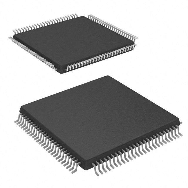
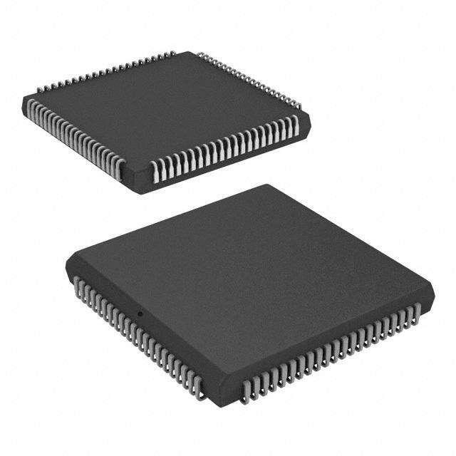
| 描述 | IC CPLD 128MC 9.1NS 100VQFP |
| 产品分类 | |
| I/O数 | 84 |
| 品牌 | Xilinx Inc |
| 数据手册 | |
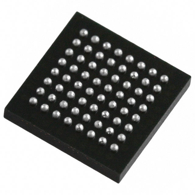
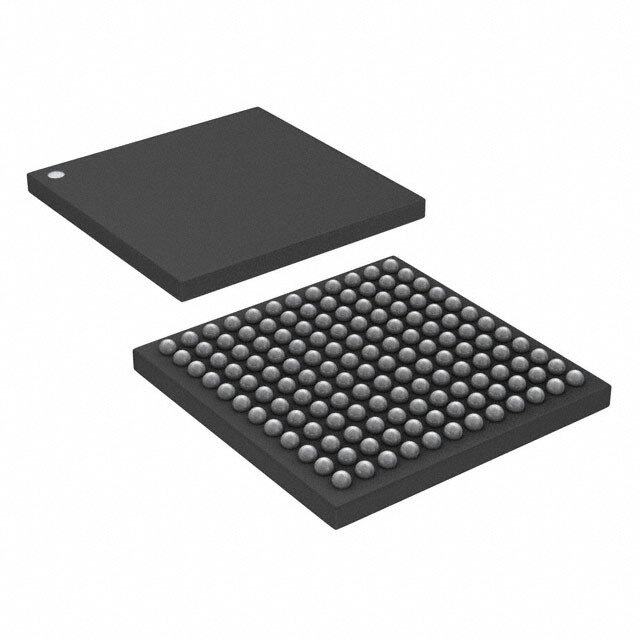
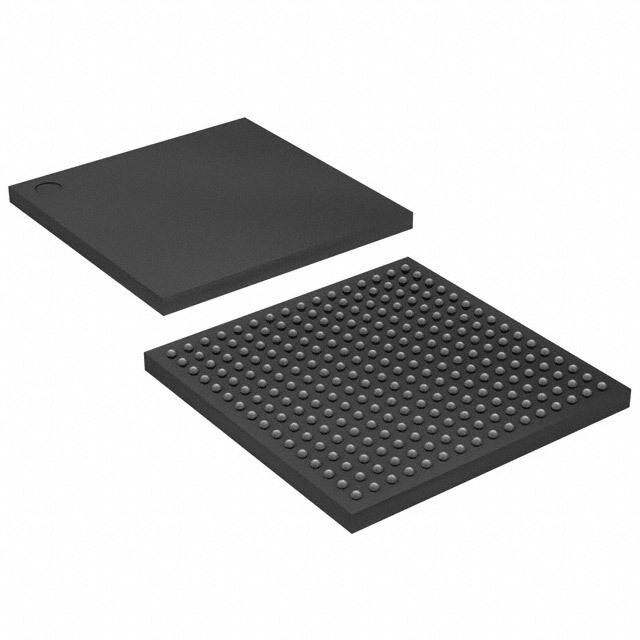
| 产品图片 |
|
| 产品型号 | XCR3128XL-10VQ100C |
| rohs | 含铅 / 不符合限制有害物质指令(RoHS)规范要求 |
| 产品系列 | CoolRunner XPLA3 |
| 产品目录页面 | |
| 供应商器件封装 | 100-VQFP(14x14) |
| 其它名称 | 122-1282 |
| 包装 | 托盘 |
| 可编程类型 | 系统内可编程(最少 1K 次编程/擦除循环) |
| 安装类型 | 表面贴装 |
| 宏单元数 | 128 |
| 封装/外壳 | 100-TQFP |
| 工作温度 | 0°C ~ 70°C |
| 延迟时间tpd(1)最大值 | 9.1ns |
| 栅极数 | 3000 |
| 标准包装 | 90 |
| 电源电压-内部 | 3 V ~ 3.6 V |
| 逻辑元件/块数 | 8 |


- 商务部:美国ITC正式对集成电路等产品启动337调查
- 曝三星4nm工艺存在良率问题 高通将骁龙8 Gen1或转产台积电
- 太阳诱电将投资9.5亿元在常州建新厂生产MLCC 预计2023年完工
- 英特尔发布欧洲新工厂建设计划 深化IDM 2.0 战略
- 台积电先进制程称霸业界 有大客户加持明年业绩稳了
- 达到5530亿美元!SIA预计今年全球半导体销售额将创下新高
- 英特尔拟将自动驾驶子公司Mobileye上市 估值或超500亿美元
- 三星加码芯片和SET,合并消费电子和移动部门,撤换高东真等 CEO
- 三星电子宣布重大人事变动 还合并消费电子和移动部门
- 海关总署:前11个月进口集成电路产品价值2.52万亿元 增长14.8%

PDF Datasheet 数据手册内容提取
0 R XCR3128XL 128 Macrocell CPLD DS016 (v2.6) March 31, 2006 Product Specification 0 14 Features Description • Low power 3.3V 128 macrocell CPLD The CoolRunner™ XPLA3 XCR3128XL device is a 3.3V • 5.5 ns pin-to-pin logic delays 128 macrocell CPLD targeted at power sensitive designs that require leading edge programmable logic solutions. A • System frequencies up to 175MHz total of eight function blocks provide 3,000 usable gates. • 128 macrocells with 3,000 usable gates Pin-to-pin propagation delays are as fast as 5.5ns with a • Available in small footprint packages maximum system frequency of 175MHz. - 144-pin TQFP (108 user I/O pins) TotalCMOS Design Technique for Fast - 144-ball CS BGA (108 user I/O) - 100-pin VQFP (84 user I/O) Zero Power • Optimized for 3.3V systems CoolRunner XPLA3 CPLDs offer a TotalCMOS™ solution, - Ultra low power operation both in process technology and design technique. Xilinx - Typical Standby Current of 17 μA at 25° C employs a cascade of CMOS gates to implement its sum of - 5V tolerant I/O pins with 3.3V core supply products instead of the traditional sense amp approach. - Advanced 0.35 micron five layer metal EEPROM This CMOS gate implementation allows Xilinx CPLDs to process offer devices that are both high performance and low power, breaking the paradigm that to have low power, you must - Fast Zero Power™ (FZP) CMOS design have low performance. Refer to Figure1 or Figure2 and technology Table1or Table2 showing the I vs. Frequency of the - 3.3V PCI electrical specification compatible outputs CC XCR3128XL TotalCMOS CPLD (data taken with eight (no internal clamp diode on any input or I/O) resetable up/down, 16-bit counters at 3.3V, 25°C). • Advanced system features - In-system programming 80 - Input registers - Predictable timing model 70 - Up to 23 available clocks per function block 60 - Excellent pin retention during design changes ) A - Full IEEE Standard 1149.1 boundary-scan (JTAG) m 50 ( - Four global clocks C C 40 - Eight product term control terms per function block al I • Fast ISP programming times pic 30 y • Port Enable pin for additional I/O T 20 • 2.7V to 3.6V supply voltage at industrial temperature range 10 • Programmable slew rate control per output 0 • Security bit prevents unauthorized access 0 20 40 60 80 100 120 140 160 • Refer to XPLA3 family data sheet (DS012) for Frequency (MHz) architecture description DS016_01_120902 Figure 1: Typical I vs. Frequency at V = 3.3V, 25°C CC CC Table 1: Typical I vs. Frequency at V = 3.3V, 25°C CC CC Frequency (MHz) 0 1 5 10 20 40 60 80 100 120 140 160 Typical I (mA) 0.017 0.5 2.48 4.97 9.89 19.7 29.5 39.1 48.7 58.0 67.3 76.8 CC © 2006 Xilinx, Inc. All rights reserved. All Xilinx trademarks, registered trademarks, patents, and disclaimers are as listed at http://www.xilinx.com/legal.htm. All other trademarks and registered trademarks are the property of their respective owners. All specifications are subject to change without notice. DS016 (v2.6) March 31, 2006 www.xilinx.com 1 Product Specification
XCR3128XL 128 Macrocell CPLD R DC Electrical Characteristics Over Recommended Operating Conditions(1) Symbol Parameter Test Conditions Typical Min. Max. Unit V (2) Output High voltage V = 3.0V to 3.6V, I = –8 mA 2.4 - V OH CC OH V = 2.7V to 3.0V, I = –8 mA 2.0 - V CC OH I = –500 μA 90% V (3) - V OH CC V Output Low voltage for 3.3V outputs I = 8 mA - 0.4 V OL OL I Input leakage current V = GND or V to 5.5V –10 10 μA IL IN CC I I/O High-Z leakage current V = GND or V to 5.5V –10 10 μA IH IN CC I (7) Standby current V = 3.6V 29 - 100 μA CCSB CC I Dynamic current(4,5) f = 1 MHz - 1 mA CC f = 50 MHz - 30 mA C Input pin capacitance(6) f = 1 MHz - 8 pF IN C Clock input capacitance(6) f = 1 MHz - 12 pF CLK C I/O pin capacitance(6) f = 1 MHz - 10 pF I/O Notes: 1. See the CoolRunner XPLA3 family data sheet (DS012) for recommended operating conditions. 2. See Figure2 for output drive characteristics of the XPLA3 family. 3. This parameter guaranteed by design and characterization, not by testing. 4. See Table1, Figure 1 for typical values. 5. This parameter measured with a 16-bit, resetable up/down counter loaded into every function block, with all outputs disabled and unloaded. Inputs are tied to V or ground. This parameter guaranteed by design and characterization, not testing. CC 6. Typical values, not tested. 7. Typical value at 70° C. 100 90 IOL(3.3V) 80 70 60 A 50 m IOH(3.3V) 40 30 IOH(2.7V) 20 10 0 0 0.5 1 1.5 2 2.5 3 3.5 4 4.5 5 Volts DS012_10_031802 Figure 2: Typical I/V Curve for the CoolRunner XPLA3 Family, 25°C 2 www.xilinx.com DS016 (v2.6) March 31, 2006 Product Specification
R XCR3128XL 128 Macrocell CPLD AC Electrical Characteristics Over Recommended Operating Conditions(1,2) -6 -7 -10 Symbol Parameter Min. Max. Min. Max. Min. Max. Unit T Propagation delay time (single p-term) - 5.5 - 7.0 - 9.1 ns PD1 T Propagation delay time (OR array)(3) - 6.0 - 7.5 - 10.0 ns PD2 T Clock to output (global synchronous pin clock) - 4.0 5.0 - 6.5 ns CO T Setup time (fast input register) 2.5 - 3.0 - 3.0 - ns SUF T (4) Setup time (single p-term) 3.5 - 4.3 - 5.4 - ns SU1 T Setup time (OR array) 4.0 - 4.8 - 6.3 - ns SU2 T (4) Hold time 0 - 0 - 0 - ns H T (4) Global Clock pulse width (High or Low) 2.5 - 3.0 - 4.0 - ns WLH T (4) P-term clock pulse width 4.0 - 5.0 - 6.0 - ns PLH T Asynchronous preset/reset pulse width (High or Low) 4.0 - 5.0 - 6.0 - ns APRPW T (4) Input rise time - 20 - 20 - 20 ns R T (4) Input fall time - 20 - 20 - 20 ns L f (4) Maximum system frequency - 175 - 119 - 95 MHz SYSTEM T (4) Configuration time(5) - 100 - 100 - 100 μs CONFIG T (4) ISP initialization time - 100 - 100 - 100 μs INIT T (4) P-term OE to output enabled - 7.5 - 9.3 - 11.2 ns POE T (4) P-term OE to output disabled(6) - 7.5 - 9.3 - 11.2 ns POD T (4) P-term clock to output - 7.0 - 8.3 - 10.7 ns PCO T (4) P-term set/reset to output valid - 8.0 - 9.3 - 11.2 ns PAO Notes: 1. Specifications measured with one output switching. 2. See the CoolRunner XPLA3 family data sheet (DS012) for recommended operating conditions. 3. See Figure6 for derating. 4. These parameters guaranteed by design and/or characterization, not testing. 5. Typical current draw during configuration is 9 mA at 3.6V. 6. Output C = 5 pF. L Internal Timing Parameters(1,2) -6 -7 -10 Symbol Parameter Min. Max. Min. Max. Min. Max. Unit Buffer Delays T Input buffer delay - 1.3 - 1.6 - 2.2 ns IN T Fast Input buffer delay - 2.3 - 3.0 - 3.1 ns FIN T Global Clock buffer delay - 0.8 - 1.0 - 1.3 ns GCK T Output buffer delay - 2.2 - 2.7 - 3.6 ns OUT T Output buffer enable/disable delay - 4.2 - 5.0 - 5.7 ns EN Internal Register and Combinatorial Delays T Latch transparent delay - 1.3 - 1.6 - 2.0 ns LDI T Register setup time 1.0 - 1.0 - 1.2 - ns SUI T Register hold time 0.3 - 0.5 - 0.7 - ns HI DS016 (v2.6) March 31, 2006 www.xilinx.com 3 Product Specification
XCR3128XL 128 Macrocell CPLD R -6 -7 -10 Symbol Parameter Min. Max. Min. Max. Min. Max. Unit T Register clock enable setup time 2.0 - 2.5 - 3.0 - ns ECSU T Register clock enable hold time 3.0 - 4.5 - 5.5 - ns ECHO T Register clock to output delay - 1.0 - 1.3 - 1.6 ns COI T Register async. S/R to output delay - 2.5 - 2.3 - 2.1 ns AOI T Register async. recovery - 4.0 - 5.0 - 6.0 ns RAI T Product term clock delay - 2.5 - 2.7 - 3.3 ns PTCK T Internal logic delay (single p-term) - 2.0 - 2.7 - 3.3 ns LOGI1 T Internal logic delay (PLA OR term) - 2.5 - 3.2 - 4.2 ns LOGI2 Feedback Delays T ZIA delay - 1.2 - 2.9 - 3.5 ns F Time Adders T Fold-back NAND delay - 2.0 - 2.5 - 3.0 ns LOGI3 T Universal delay - 1.7 - 2.2 - 2.7 ns UDA T Slew rate limited delay - 4.0 - 5.0 - 6.0 ns SLEW Notes: 1. These parameters guaranteed by design and/or characterization, not testing. 2. See the CoolRunner XPLA family data sheet (DS012) for timing model. 4 www.xilinx.com DS016 (v2.6) March 31, 2006 Product Specification
R XCR3128XL 128 Macrocell CPLD Switching Characteristics VCC S1 Component Values R1 390Ω R2 390Ω R1 C1 35 pF V IN V OUT Measurement S1 S2 R2 C1 TPOE (High) Open Closed TPOE (Low) Closed Open TP Closed Closed Note: For TPOD, C1 = 5 pF. Delay measured at S2 output level of VOL + 300 mV, VOH – 300 mV. DS016_03_102401 Figure 3: AC Load Circuit 6.0 +3.0V 90% 5.8 10% 5.6 0V ns 5.4 TR TL 1.5 ns 1.5 ns 5.2 Measurements: All circuit delays are measured at the +1.5V level of inputs and outputs, unless otherwise specified. 5.0 DS016_05_042800 Figure 5: Voltage Waveform 4.8 1 2 4 8 16 Number of Adjacent Outputs Switching DS016_04a_120902 Figure 4: Derating Curve for T PD2 DS016 (v2.6) March 31, 2006 www.xilinx.com 5 Product Specification
XCR3128XL 128 Macrocell CPLD R Pin Descriptions Table 3: XCR3128XL I/O Pins (Continued) Function Table 2: XCR3128XL User I/O Pins Block Macrocell VQ100 CS144 TQ144 VQ100 CS144 TQ144 3 1 - G13 90 Total User I/O Pins 84 108 108 3 2 62(1) G12(1) 89(1) 3 3 61 H13 88 Table 3: XCR3128XL I/O Pins 3 4 60 H12 87 Function Block Macrocell VQ100 CS144 TQ144 3 5 - H11 86 1 1 - B12 106 3 6 58 J13 84 1 2 73(1) D11(1) 104(1) 3 7 57 J12 83 3 8 - - - 1 3 72 D12 102 3 9 - - - 1 4 71 D13 101 3 10 - - - 1 5 70 E10 100 3 11 56 J11 82 1 6 69 E11 99 3 12 55 J10 81 1 7 68 E12 98 3 13 54 K13 80 1 8 - - - 3 14 53 K12 79 1 9 - - - 3 15 52 K11 78 1 10 - - - 3 16 - K10 77 1 11 67 E13 97 4 1 - M8 60 1 12 - F10 96 4 2 40 L8 61 1 13 65 F12 94 4 3 41 K8 62 1 14 64 F13 93 4 4 42 N9 63 1 15 63 G10 92 4 5 44 L9 65 1 16 - G11 91 4 6 45 K9 66 2 1 75 A13 107 4 7 46 N10 67 2 2 76 A12 109 4 8 - - - 2 3 77 B11 110 4 9 - - - 2 4 78 A11 111 4 10 - - - 2 5 79 D10 112 4 11 47 M10 68 2 6 80 C10 113 4 12 48 L10 69 2 7 81 B10 114 4 13 49 N11 70 2 8 - - - 4 14 50 M11 71 2 9 - - - 4 15 - L11 72 2 10 - - - 4 16 - M12 74 2 11 83 D9 116 5 1 2 A1 1 2 12 84 C9 117 5 2 1 A2 143 2 13 85 B9 118 5 3 100 C3 142 2 14 - A9 119 5 4 99 B3 141 2 15 - D8 120 5 5 98 A3 140 2 16 - C8 121 6 www.xilinx.com DS016 (v2.6) March 31, 2006 Product Specification
R XCR3128XL 128 Macrocell CPLD Table 3: XCR3128XL I/O Pins (Continued) Table 3: XCR3128XL I/O Pins (Continued) Function Function Block Macrocell VQ100 CS144 TQ144 Block Macrocell VQ100 CS144 TQ144 5 6 97 C4 139 7 11 30 N4 42 5 7 96 B4 138 7 12 29 M4 41 5 8 - - - 7 13 28 L4 40 5 9 - - - 7 14 27 K4 39 5 10 - - - 7 15 - N3 38 5 11 - A4 137 7 16 - M3 37 5 12 - D5 136 8 1 - H1 18 5 13 94 B5 134 8 2 15(1) H2(1) 20(1) 5 14 93 A5 133 8 3 16 H3 21 5 15 92 D6 132 8 4 17 H4 22 5 16 - C6 131 8 5 - J1 23 6 1 - B1 2 8 6 19 J3 25 6 2 4(1) D2(1) 4(1) 8 7 20 J4 26 6 3 5 D1 5 8 8 - - - 6 4 6 E4 6 8 9 - - - 6 5 7 E3 7 8 10 - - - 6 6 8 E2 8 8 11 21 K1 27 6 7 9 E1 9 8 12 22 K2 28 6 8 - - - 8 13 23 K3 29 6 9 - - - 8 14 24 L1 30 6 10 - - - 8 15 25 M2 31 6 11 10 F4 10 8 16 - N1 32 6 12 - F3 11 Notes: 1. JTAG pins 6 13 - F2 12 6 14 12 G2 14 6 15 13 G1 15 6 16 14 G3 16 7 1 - N7 56 7 2 37 M7 55 7 3 36 N6 54 7 4 35 M6 53 7 5 33 M5 46 7 6 32 L5 45 7 7 31 K5 44 7 8 - - - 7 9 - - - 7 10 - - - DS016 (v2.6) March 31, 2006 www.xilinx.com 7 Product Specification
XCR3128XL 128 Macrocell CPLD R Table 4: XCR3128XL Global, JTAG, Port Enable, Power, Table 4: XCR3128XL Global, JTAG, Port Enable, Power, and No Connect Pins and No Connect Pins Pin Type VQ100 CS144 TQ144 Pin Type VQ100 CS144 TQ144 IN0 / CLK0 90 D7 128 GND 26, 38, 43, A6, A8, C5, 3, 17, 33, 59, 74, 86, C13, D3, 52, 57, 59, IN1 / CLK1 89 C7 127 95 G4, H10, 64, 85, 105, IN2 / CLK2 88 A7 126 L6, L7, M9, 124, 129, N2, N8 135 IN3 / CLK3 87 B7 125 No Connects - B13, C1, 19, 34, 35, TCK 62 G12 89 C2, C11, 36, 43, 47, TDI 4 D2 4 C12, L2, L3, 48, 49, 75, TDO 73 D11 104 L12, M1, 103, 108, M13, N13 122 TMS 15 H2 20 Notes: PORT_EN 11(1) F1(1) 13(1) 1. Port Enable is brought High to enable JTAG pins when JTAG pins are used as I/O. See family data sheet (DS012) for full Vcc 3, 18, 34, A10, B2, B6, 24, 50, 51, explanation. 39, 51, 66, B8, D4, F11, 58, 73, 76, 82, 91 J2, K6, K7, 95, 115, L13, N5, 123, 130, N12 144 8 www.xilinx.com DS016 (v2.6) March 31, 2006 Product Specification
R XCR3128XL 128 Macrocell CPLD Device Part Marking and Ordering Combination Information R Device Type XCRxxxxXL Package TQ144 This line not Speed 7C related to device part number Operating Range 1 Sample package with part marking. Speed Device Ordering and (pin-to-pin Pkg. No. of Operating Part Marking Number delay) Symbol Pins Package Type Range(1) XCR3128XL-6VQ100C 6 ns VQ100 100 Very Thin Quad Flat Package (VQFP) C XCR3128XL-6VQG100C 6 ns VQG100 100 Very Thin Quad Flat Package (VQFP); Pb-Free C XCR3128XL-6CS144C 6 ns CS144 144 Chip Scale Package (CSP) C XCR3128XL-6CSG144C 6 ns CSG144 144 Chip Scale Package (CSP); Pb-Free C XCR3128XL-6TQ144C 6 ns TQ144 144 Thin Quad Flat Pack (TQFP) C XCR3128XL-6TQG144C 6 ns TQG144 144 Thin Quad Flat Pack (TQFP); Pb-Free C XCR3128XL-7VQ100C 7.5 ns VQ100 100 Very Thin Quad Flat Package (VQFP) C XCR3128XL-7VQG100C 7.5 ns VQG100 100 Very Thin Quad Flat Package (VQFP); Pb-Free C XCR3128XL-7CS144C 7.5 ns CS144 144 Chip Scale Package (CSP) C XCR3128XL-7CSG144C 7.5 ns CSG144 144 Chip Scale Package (CSP); Pb-Free C XCR3128XL-7TQ144C 7.5 ns TQ144 144 Thin Quad Flat Pack (TQFP) C XCR3128XL-7TQG144C 7.5 ns TQG144 144 Thin Quad Flat Pack (TQFP); Pb-Free C XCR3128XL-7VQ100I 7.5 ns VQ100 100 Very Thin Quad Flat Package (VQFP) I XCR3128XL-7VQG100I 7.5 ns VQG100 100 Very Thin Quad Flat Package (VQFP); Pb-Free I XCR3128XL-7CS144I 7.5 ns CS144 144 Chip Scale Package (CSP) I XCR3128XL-7CSG144I 7.5 ns CSG144 144 Chip Scale Package (CSP); Pb-Free I XCR3128XL-7TQ144I 7.5 ns TQ144 144 Thin Quad Flat Pack (TQFP) I XCR3128XL-7TQG144I 7.5 ns TQG144 144 Thin Quad Flat Pack (TQFP); Pb-Free I XCR3128XL-10VQ100C 10 ns VQ100 100 Very Thin Quad Flat Package (VQFP) C XCR3128XL-10VQG100C 10 ns VQG100 100 Very Thin Quad Flat Package (VQFP); Pb-Free C XCR3128XL-10CS144C 10 ns CS144 144 Chip Scale Package (CSP) C XCR3128XL-10CSG144C 10 ns CSG144 144 Chip Scale Package (CSP); Pb-Free C XCR3128XL-10TQ144C 10 ns TQ144 144 Thin Quad Flat Pack (TQFP) C XCR3128XL-10TQG144C 10 ns TQG144 144 Thin Quad Flat Pack (TQFP); Pb-Free C DS016 (v2.6) March 31, 2006 www.xilinx.com 9 Product Specification
XCR3128XL 128 Macrocell CPLD R Speed Device Ordering and (pin-to-pin Pkg. No. of Operating Part Marking Number delay) Symbol Pins Package Type Range(1) XCR3128XL-10VQ100I 10 ns VQ100 100 Very Thin Quad Flat Package (VQFP) I XCR3128XL-10VQG100I 10 ns VQG100 100 Very Thin Quad Flat Package (VQFP); Pb-Free I XCR3128XL-10CS144I 10 ns CS144 144 Chip Scale Package (CSP) I XCR3128XL-10CSG144I 10 ns CSG144 144 Chip Scale Package (CSP); Pb-Free I XCR3128XL-10TQ144I 10 ns TQ144 144 Thin Quad Flat Pack (TQFP) I XCR3128XL-10TQG144I 10 ns TQG144 144 Thin Quad Flat Pack (TQFP); Pb-Free I Notes: 1. C = Commercial: T = 0° to +70°C; I = Industrial: T = –40° to +85°C A A Warranty Disclaimer THESE PRODUCTS ARE SUBJECT TO THE TERMS OF THE XILINX LIMITED WARRANTY WHICH CAN BE VIEWED AT http://www.xilinx.com/warranty.htm. THIS LIMITED WARRANTY DOES NOT EXTEND TO ANY USE OF THE PRODUCTS IN AN APPLICATION OR ENVIRONMENT THAT IS NOT WITHIN THE SPECIFICATIONS STATED ON THE THEN-CURRENT XILINX DATA SHEET FOR THE PRODUCTS. PRODUCTS ARE NOT DESIGNED TO BE FAIL-SAFE AND ARE NOT WARRANTED FOR USE IN APPLICATIONS THAT POSE A RISK OF PHYSICAL HARM OR LOSS OF LIFE. USE OF PRODUCTS IN SUCH APPLICATIONS IS FULLY AT THE RISK OF CUSTOMER SUBJECT TO APPLICABLE LAWS AND REGULATIONS. Additional Information CoolRunner XPLA3 Data Sheets and Application Notes Device Package User Guide Device Packages Revision History The following table shows the revision history for this document. Date Version Revision 04/07/00 1.0 Initial Xilinx release. 05/03/00 1.1 Minor updates and added Boundary Scan to pinout table. 11/20/00 1.2 Updated pinout tables; corrected note in Table4 to read: "port enable pin is brought High". 12/08/00 1.3 Updated pinout tables. 01/17/01 1.4 Removed Timing Model. 04/11/01 1.5 Added Typical I/V curve, Figure2; added Table2: Total User I/O; changed V spec. OH 04/19/01 1.6 Updated Typical I/V curve, Figure2: added voltage levels. 08/10/01 1.7 Moved Figure1 and Table1 to first page. Changed VQ144 to VQ100 in Table2. 01/08/02 1.8 Updated T and T spec to match software timing. Added single p-term setup time (T ) to SUF FIN SU1 AC Table, renamed T to T for setup time through the OR array. Added T spec. Updated SU SU2 INIT T spec. Updated T spec to correct a typo. Updated AC Load Circuit diagram to more CONFIG HI closely resemble true test conditions, added note for T delay measurement. POD 01/27/03 1.9 Updated product availability and AC/DC parameters for -6 Commercial and -7 Industrial devices. Updated T (added T ), T , T , T . Updated I vs. Frequency Curve for -6 device; PCO PTCK CONFIG INIT F CC updated system frequency to 175 MHz; removed Advance Information from -6 device; updated Derating Curve for -6 device. Updated Ordering Information format. 10 www.xilinx.com DS016 (v2.6) March 31, 2006 Product Specification
R XCR3128XL 128 Macrocell CPLD Date Version Revision 07/15/03 2.0 Updated test conditions for I and I . IL IH 08/21/03 2.1 Updated Package Device Marking Pin 1 orientation. 02/13/04 2.2 Added soldering temperature. Added links to application notes and data sheets. 07/09/04 2.3 Updated the following specifications based on characterization of product after move to UMC fabrication for all family members: V , T . Deleted derating curve for T for MOSIV OH LOGI3 PD2 fabricated material. 11/11/04 2.4 Moved from Preliminary Product Specification to Product Specification. 04/08/05 2.5 Added I Typical and T specifications. Removed T specification. CCSB APRPW SOL 03/31/06 2.6 Added Warranty Disclaimer. Added Pb-Free information to ordering table. DS016 (v2.6) March 31, 2006 www.xilinx.com 11 Product Specification