ICGOO在线商城 > 74HCT126T14-13

 Datasheet下载
- 型号: 74HCT126T14-13
- 制造商: Diodes Inc.
- 库位|库存: xxxx|xxxx
- 要求:
| 数量阶梯 | 香港交货 | 国内含税 |
| +xxxx | $xxxx | ¥xxxx |
查看当月历史价格
查看今年历史价格
74HCT126T14-13产品简介:
ICGOO电子元器件商城为您提供74HCT126T14-13由Diodes Inc.设计生产,在icgoo商城现货销售,并且可以通过原厂、代理商等渠道进行代购。 提供74HCT126T14-13价格参考以及Diodes Inc.74HCT126T14-13封装/规格参数等产品信息。 你可以下载74HCT126T14-13参考资料、Datasheet数据手册功能说明书, 资料中有74HCT126T14-13详细功能的应用电路图电压和使用方法及教程。
| 参数 | 数值 |
| 产品目录 | 集成电路 (IC) |
| 描述 | IC GATE 2.5K TSSOP14 |
| 产品分类 | |
| 品牌 | Diodes Incorporated |
| 数据手册 | |
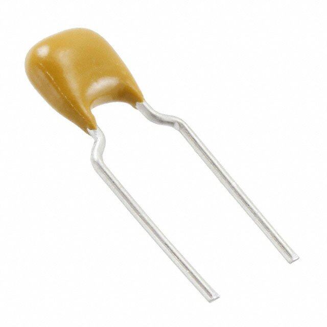
| 产品图片 |
|
| 产品型号 | 74HCT126T14-13 |
| rohs | 无铅 / 符合限制有害物质指令(RoHS)规范要求 |
| RoHS指令信息 | http://diodes.com/download/4349 |
| 产品系列 | 74HCT |
| 供应商器件封装 | 14-TSSOP |
| 元件数 | 4 |
| 其它名称 | 74HCT126T14-13DIDKR |
| 包装 | Digi-Reel® |
| 安装类型 | 表面贴装 |
| 封装/外壳 | 14-TSSOP(0.173",4.40mm 宽) |
| 工作温度 | -40°C ~ 125°C |
| 标准包装 | 1 |
| 每元件位数 | 1 |
| 电压-电源 | 4.5 V ~ 5.5 V |
| 电流-输出高,低 | 4mA,4mA |
| 逻辑类型 | 施密特触发器 - 缓冲器,驱动器 |


- 商务部:美国ITC正式对集成电路等产品启动337调查
- 曝三星4nm工艺存在良率问题 高通将骁龙8 Gen1或转产台积电
- 太阳诱电将投资9.5亿元在常州建新厂生产MLCC 预计2023年完工
- 英特尔发布欧洲新工厂建设计划 深化IDM 2.0 战略
- 台积电先进制程称霸业界 有大客户加持明年业绩稳了
- 达到5530亿美元!SIA预计今年全球半导体销售额将创下新高
- 英特尔拟将自动驾驶子公司Mobileye上市 估值或超500亿美元
- 三星加码芯片和SET,合并消费电子和移动部门,撤换高东真等 CEO
- 三星电子宣布重大人事变动 还合并消费电子和移动部门
- 海关总署:前11个月进口集成电路产品价值2.52万亿元 增长14.8%


PDF Datasheet 数据手册内容提取
74HCT126 QUADRUPLE 3-STATE BUFFERS OE HIGH Description Pin Assignments The 74HCT126 provides provides four independent buffer gates with 3-state outputs. Each buffer has a separate enable pin that if driven with a low logic level places the corresponding output in the high impedance state. The device is designed for operation with a power supply range of 4.5V to 5.5V. Features • Wide Supply Voltage Range from 4.5V to 5.5V • Pin Compatible with Low Power Schottky (LSTTL) • Inputs Are TTL Voltage Level Compatible • Sinks or sources 4mA at VCC = 4.5V • CMOS low power consumption • Schmitt Trigger Action at All Inputs • ESD Protection Exceeds JESD 22 (cid:131) 200-V Machine Model (A115-A) Applications (cid:131) 2000-V Human Body Model (A114-A) • General Purpose Logic (cid:131) Exceeds 1000-V Charged Device Model (C101C) • Wide array of products such as: • Range of Package Options SO-14 and TSSOP-14 (cid:131) PCs, networking, notebooks, netbooks • Totally Lead-Free & Fully RoHS Compliant (Notes 1 & 2) (cid:131) Computer peripherals, hard drives, CD/DVD ROM • Halogen and Antimony Free. “Green” Device (Note 3) (cid:131) TV, DVD, DVR, set top box Notes: 1. No purposely added lead. Fully EU Directive 2002/95/EC (RoHS) & 2011/65/EU (RoHS 2) compliant. 2. See http://www.diodes.com for more information about Diodes Incorporated’s definitions of Halogen- and Antimony-free, "Green" and Lead-free. 3. Halogen- and Antimony-free "Green” products are defined as those which contain <900ppm bromine, <900ppm chlorine (<1500ppm total Br + Cl) and <1000ppm antimony compounds. 74HCT126 1 of 8 January 2013 Document number: DS35337 Rev. 3 - 2 www.diodes.com © Diodes Incorporated
74HCT126 Pin Descriptions Pin Number Pin Name Description 1 1OE Data Enable Input (active high) 2 1A Data Input 3 1Y Data Output 4 2OE Data Enable Input (active high) 5 2A Data Input 6 2Y Data Output 7 GND Ground 8 3Y Data Output 9 3A Data Input 10 3OE Data Enable Input (active high) 11 4Y Data Output 12 4A Data Input 13 4OE Data Enable Input (active high) 14 VCC Supply Voltage Logic Diagram Function Table Inputs Output OE A Y H H H H L L L X Z 74HCT126 2 of 8 January 2013 Document number: DS35337 Rev. 3 - 2 www.diodes.com © Diodes Incorporated
74HCT126 Absolute Maximum Ratings (Note 4) (@TA = +25°C, unless otherwise specified.) Symbol Description Rating Unit ESD HBM Human Body Model ESD Protection 2 KV ESD CDM Charged Device Model ESD Protection 1 KV ESD MM Machine Model ESD Protection 200 V VCC Supply Voltage Range -0.5 to +7.0 V VI Input Voltage Range (Note 5) -0.5 to +7.0 V IIK Input Clamp Current VI < -0.5V or Vi > VCC +0.5V ±20 mA IOK Output Clamp Current VO < -0.5V or VO > VCC +0.5V ±20 mA IO Continuous Output Current -0.5V < VO VCC +0.5V +/-25 mA ICC Continuous Current Through VCC 50 mA IGND Continuous Current Through GND -50 mA TJ Operating Junction Temperature -40 to +150 °C TSTG Storage Temperature -65 to +150 °C PTOT Total Power Dissipation 500 mW Notes: 4. Stresses beyond the absolute maximum may result in immediate failure or reduced reliability. These are stress values and device operation should be within recommend values. 5. Input Voltage cannot exceed VCC to the extent the Maximum clamp current is exceeded. Recommended Operating Conditions (Note 6) (@TA = +25°C, unless otherwise specified.) Symbol Parameter Conditions Min Max Unit VCC Supply Voltage 4.5 5.5 V VI Input Voltage 0 VCC V VO Output Voltage 0 VCC V Δt/ΔV Input Transition Rise or Fall Rate VCC = 4.5V to 5.5V 500 ns/V TA Operating Free-Air Temperature -40 +125 °C Note: 6. Unused inputs should be held at VCC or Ground. Electrical Characteristics (@TA = +25°C, unless otherwise specified.) Symbol Parameter Test Conditions VCC TA = -40°C to +85°C TA = -40°C to +125°C Unit Min Max Min Max High-level Input VIH Voltage 4.5V to 5.5V 2.0 2.0 V Low-level Input VIL Voltage 4.5V to 5.5V 0.8 0.8 V High-level Output IOH = -20μA 4.5V 4.4 4.4 VOH Voltage IOH = -4mA 4.5V 3.84 3.70 V Low-level Output IOL = 20μA 4.5V 0.1 0.1 VOL Voltage IOL = 4.0mA 4.5V 0.33 0.4 V Z State Leakage IOZ Current VO = 0 to 5.5V 5.5V ± 5.0 ± 10 μA II Input Current VI = GND to 6.0V 6.0V ± 1 ± 1 μA ICC Supply Current VI = GND or VCC, IO = 0 6.0V 20 40 μA ΔICC ACdudrrietinotn al Supply OOnthee Irn Ppiunts a at tV VCCCC - o2r.1 GVN D 4.5V to 5.5V 675 735 μA 74HCT126 3 of 8 January 2013 Document number: DS35337 Rev. 3 - 2 www.diodes.com © Diodes Incorporated
74HCT126 Switching Characteristics Symbol Parameter Test Conditions VCC TA = +25°C -40°C to +85°C -40°C to +125°C Unit Min Typ Max Max Max Propagation tPD Delay AN to YN — 15 25 31 38 ns Enable Time tEN OEN to YN Figure 1 4.5V — 15 28 35 42 ns DisableTime CL = 50pF tDIS OEN to YN — 15 25 31 38 ns tt Transition Time — 5 12 15 18 ns Operating Characteristics (@TA = +25°C, unless otherwise specified.) Parameter Test Conditions VCC = 5.5V Unit Typ Power dissipation Cpd capacitance per gate f = 1MHz 24 pF CI Input Capacitance VI = VCC – or GND 3.5 pF Parameter Measurement Information TEST Condition tPLZ (see Notes D and E) Vload tPZL(see Notes D and F) Vload Inputs VCC VM VLOAD CL RL V∆ VI tr/tf 4.5V 1.5V ≤6ns 3.0V 2 X VCC 50pF 2KΩ 10% of VCC Voltage Waveform Pulse Duration Voltage Waveform Propagation Delay Times Notes: A. Includes test lead and test apparatus capacitance. B. All pulses are supplied at pulse repetition rate ≤ 1 MHz. C. The inputs are measured one at a time with one transition per measurement. D. For the open drain device tPLZ and tPZL are the same as tPD. E. tPZL is measured at VM. D. tPLZ is measured at VOL +V∆. F. A Thevenin equivalent load may be used in place of VCC X 2 and resistor divider. Figure 1 Load Circuit and Voltage Waveforms 74HCT126 4 of 8 January 2013 Document number: DS35337 Rev. 3 - 2 www.diodes.com © Diodes Incorporated
74HCT126 Ordering Information 7” Tape and Reel Device Package Code Packaging Quantity Part Number Suffix 74HCT126S14-13 S14 SO-14 2500/Tape & Reel -13 74HCT126T14-13 T14 TSSOP-14 2500/Tape & Reel -13 Marking Information (1) SO-14, TSSOP-14 Part Number Package 74HCT126S14 SO-14 74HCT126T14 TSSOP-14 74HCT126 5 of 8 January 2013 Document number: DS35337 Rev. 3 - 2 www.diodes.com © Diodes Incorporated
74HCT126 Package Outline Dimensions (All dimensions in mm.) Please see AP02002 at http://www.diodes.com/datasheets/ap02002.pdf for latest version. Package Type: SO-14 SO-14 Dim Min Max E H Gauge Plane A 1.47 1.73 A1 0.10 0.25 L θ A2 1.45 Typ B 0.33 0.51 Detail “A” D 8.53 8.74 E 3.80 3.99 7°(4x) D A2 A He 5.810. 27 Ty6p. 20 L 0.38 1.27 θ 0° 8° B e Detail “A” All Dimensions in mm A1 Package Type: TSSOP-14 TSSOP-14 5 Dim Min Max 02. a1 7° (4X) Pin# 1 Indent B L GSeaautgineg P Plalannee a2 0° 8° F1 A 4.9 5.10 2 a B 4.30 4.50 F C ⎯ 1.2 Detail ‘A’ D 0.8 1.05 F 1.00 Typ G K F1 0.45 0.75 A G 0.65 Typ K 0.19 0.30 a1 D L 6.40 Typ C All Dimensions in mm Detail ‘A’ 74HCT126 6 of 8 January 2013 Document number: DS35337 Rev. 3 - 2 www.diodes.com © Diodes Incorporated
74HCT126 Suggested Pad Layout Please see AP02001 at http://www.diodes.com/datasheets/ap02001.pdf for latest version. Package Type: SO-14 X Dimensions Value (in mm) X 0.60 Y 1.50 C1 5.4 C1 C2 1.27 C2 Y Package Type: TSSOP-14 X Dimensions Value (in mm) X 0.45 Y 1.45 C1 5.9 C1 C2 0.65 C2 Y 74HCT126 7 of 8 January 2013 Document number: DS35337 Rev. 3 - 2 www.diodes.com © Diodes Incorporated
74HCT126 IMPORTANT NOTICE DIODES INCORPORATED MAKES NO WARRANTY OF ANY KIND, EXPRESS OR IMPLIED, WITH REGARDS TO THIS DOCUMENT, INCLUDING, BUT NOT LIMITED TO, THE IMPLIED WARRANTIES OF MERCHANTABILITY AND FITNESS FOR A PARTICULAR PURPOSE (AND THEIR EQUIVALENTS UNDER THE LAWS OF ANY JURISDICTION). Diodes Incorporated and its subsidiaries reserve the right to make modifications, enhancements, improvements, corrections or other changes without further notice to this document and any product described herein. Diodes Incorporated does not assume any liability arising out of the application or use of this document or any product described herein; neither does Diodes Incorporated convey any license under its patent or trademark rights, nor the rights of others. Any Customer or user of this document or products described herein in such applications shall assume all risks of such use and will agree to hold Diodes Incorporated and all the companies whose products are represented on Diodes Incorporated website, harmless against all damages. Diodes Incorporated does not warrant or accept any liability whatsoever in respect of any products purchased through unauthorized sales channel. Should Customers purchase or use Diodes Incorporated products for any unintended or unauthorized application, Customers shall indemnify and hold Diodes Incorporated and its representatives harmless against all claims, damages, expenses, and attorney fees arising out of, directly or indirectly, any claim of personal injury or death associated with such unintended or unauthorized application. Products described herein may be covered by one or more United States, international or foreign patents pending. Product names and markings noted herein may also be covered by one or more United States, international or foreign trademarks. This document is written in English but may be translated into multiple languages for reference. Only the English version of this document is the final and determinative format released by Diodes Incorporated. LIFE SUPPORT Diodes Incorporated products are specifically not authorized for use as critical components in life support devices or systems without the express written approval of the Chief Executive Officer of Diodes Incorporated. As used herein: A. Life support devices or systems are devices or systems which: 1. are intended to implant into the body, or 2. support or sustain life and whose failure to perform when properly used in accordance with instructions for use provided in the labeling can be reasonably expected to result in significant injury to the user. B. A critical component is any component in a life support device or system whose failure to perform can be reasonably expected to cause the failure of the life support device or to affect its safety or effectiveness. Customers represent that they have all necessary expertise in the safety and regulatory ramifications of their life support devices or systems, and acknowledge and agree that they are solely responsible for all legal, regulatory and safety-related requirements concerning their products and any use of Diodes Incorporated products in such safety-critical, life support devices or systems, notwithstanding any devices- or systems-related information or support that may be provided by Diodes Incorporated. Further, Customers must fully indemnify Diodes Incorporated and its representatives against any damages arising out of the use of Diodes Incorporated products in such safety-critical, life support devices or systems. Copyright © 2013, Diodes Incorporated www.diodes.com 74HCT126 8 of 8 January 2013 Document number: DS35337 Rev. 3 - 2 www.diodes.com © Diodes Incorporated
Mouser Electronics Authorized Distributor Click to View Pricing, Inventory, Delivery & Lifecycle Information: D iodes Incorporated: 74HCT126T14-13 74HCT126S14-13