ICGOO在线商城 > 集成电路(IC) > PMIC - 稳压器 - 线性 > ADP1712AUJZ-R7
 Datasheet下载
- 型号: ADP1712AUJZ-R7
- 制造商: Analog
- 库位|库存: xxxx|xxxx
- 要求:
| 数量阶梯 | 香港交货 | 国内含税 |
| +xxxx | $xxxx | ¥xxxx |
查看当月历史价格
查看今年历史价格
ADP1712AUJZ-R7产品简介:
ICGOO电子元器件商城为您提供ADP1712AUJZ-R7由Analog设计生产,在icgoo商城现货销售,并且可以通过原厂、代理商等渠道进行代购。 ADP1712AUJZ-R7价格参考¥5.65-¥7.06。AnalogADP1712AUJZ-R7封装/规格:PMIC - 稳压器 - 线性, Linear Voltage Regulator IC Positive Adjustable 1 Output 300mA TSOT-5。您可以下载ADP1712AUJZ-R7参考资料、Datasheet数据手册功能说明书,资料中有ADP1712AUJZ-R7 详细功能的应用电路图电压和使用方法及教程。
ADP1712AUJZ-R7是Analog Devices Inc.推出的一款低压差线性稳压器(LDO),适用于对电源噪声敏感、空间受限且需要高稳定性的便携式电子设备。其典型应用场景包括智能手机、平板电脑、可穿戴设备(如智能手表和健康监测设备)以及物联网(IoT)终端节点。

该器件具有低静态电流(典型值40μA),有助于延长电池供电设备的续航时间,非常适合电池长期供电的应用。其超小封装(TSOT-23-5)节省PCB空间,适合高密度布局的便携产品。输出电压精度高达±2%,支持1.8V至3.3V的固定输出选项,可为微处理器、传感器、射频模块和低功耗FPGA等提供稳定、干净的电源。

此外,ADP1712具备良好的瞬态响应和低噪声特性(约30μVrms),适用于为高精度模拟电路(如ADC、DAC或传感器信号调理电路)供电,有效减少电源干扰。内置过温保护和过流保护功能,提升系统可靠性。在工业自动化、医疗监测设备及消费类电子产品中,ADP1712AUJZ-R7因其高效率、低噪声和小型化优势,成为理想的后级稳压解决方案。
| 参数 | 数值 |
| 产品目录 | 集成电路 (IC)半导体 |
| 描述 | IC REG LDO ADJ 0.3A TSOT23-5线性稳压器 IC 300mA LDO CMOS |
| 产品分类 | |
| 品牌 | Analog Devices Inc |
| 产品手册 | |
| 产品图片 |
|
| rohs | 符合RoHS无铅 / 符合限制有害物质指令(RoHS)规范要求 |
| 产品系列 | 电源管理 IC,线性稳压器,Analog Devices ADP1712AUJZ-R7- |
| 数据手册 | |
| 产品型号 | ADP1712AUJZ-R7 |
| 产品培训模块 | http://www.digikey.cn/PTM/IndividualPTM.page?site=cn&lang=zhs&ptm=19143 |
| 产品目录页面 | |
| 产品种类 | |
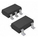
| 供应商器件封装 | TSOT-5 |
| 其它名称 | ADP1712AUJZ-R7TR |
| 包装 | 带卷 (TR) |
| 商标 | Analog Devices |
| 安装类型 | 表面贴装 |
| 安装风格 | SMD/SMT |
| 封装 | Reel |
| 封装/外壳 | SOT-23-5 细型,TSOT-23-5 |
| 封装/箱体 | TSOT-5 |
| 工作温度 | -40°C ~ 125°C |
| 工厂包装数量 | 3000 |
| 最大工作温度 | + 125 C |
| 最大输入电压 | 5.5 V |
| 最小工作温度 | - 40 C |
| 最小输入电压 | 2.5 V |
| 标准包装 | 3,000 |
| 电压-跌落(典型值) | 0.17V @ 300mA |
| 电压-输入 | 2.5 V ~ 5.5 V |
| 电压-输出 | 0.8 V ~ 5 V |
| 电流-输出 | 300mA |
| 电流-限制(最小值) | 380mA |
| 稳压器拓扑 | 正,可调式 |
| 稳压器数 | 1 |
| 系列 | ADP1712 |
| 视频文件 | http://www.digikey.cn/classic/video.aspx?PlayerID=1364138032001&width=640&height=505&videoID=2245193149001 |
| 输出电流 | 300 mA |
| 配用 | /product-detail/zh/ADP1712-3.3-EVALZ/ADP1712-3.3-EVALZ-ND/1680438/product-detail/zh/ADP1712-EVALZ/ADP1712-EVALZ-ND/1692337 |


- 商务部:美国ITC正式对集成电路等产品启动337调查
- 曝三星4nm工艺存在良率问题 高通将骁龙8 Gen1或转产台积电
- 太阳诱电将投资9.5亿元在常州建新厂生产MLCC 预计2023年完工
- 英特尔发布欧洲新工厂建设计划 深化IDM 2.0 战略
- 台积电先进制程称霸业界 有大客户加持明年业绩稳了
- 达到5530亿美元!SIA预计今年全球半导体销售额将创下新高
- 英特尔拟将自动驾驶子公司Mobileye上市 估值或超500亿美元
- 三星加码芯片和SET,合并消费电子和移动部门,撤换高东真等 CEO
- 三星电子宣布重大人事变动 还合并消费电子和移动部门
- 海关总署:前11个月进口集成电路产品价值2.52万亿元 增长14.8%


PDF Datasheet 数据手册内容提取
300 mA, Low Dropout CMOS Linear Regulator ADP1712/ADP1713/ADP1714 FEATURES TYPICAL APPLICATION CIRCUITS Maximum output current: 300 mA ADP1712 Input voltage range: 2.5 V to 5.5 V VIN = 5V VOUT = 3.3V 1 IN OUT 5 Light load efficient 2.2µF 2.2µF I = 75 μA with 100 μA load 2 GND GND LVoewry s lhouwt ddorowpno cuut rvroelntta:g <e1: 1μ7A0 mV @ 300 mA load 3 EN SS 4 10nF 06455-001 Initial accuracy: ±1% Figure 1. ADP1712 with Fixed Output Voltage and Soft-Start Capacitor, 3.3 V Accuracy over line, load, and temperature: ±2% ADP1712 16 fixed output voltage options with soft start: VIN = 5.5V ADJUSTABLE VOUT = 0.8V(1 + R1/R2) 0.75 V to 3.3 V (ADP1712) 1 IN OUT 5 Adjustable output voltage option: 0.8 V to 5.0 V 2.2µF 2.2µF 2 GND (ADP1712 Adjustable) R1 16 fixed output voltage options with reference bypass: 3 EN ADJ 4 160 f.i7x5ed V o tou t3p.u3t V v (oAltDaPg1e7 o1p3t)i ons with tracking: R2 06455-002 Figure 2. ADP1712 with Adjustable Output Voltage, 0.8 V to 5.0 V 0.75 V to 3.3 V (ADP1714) Low output noise: 40 μV rms ADP1713 High PSRR: 72 dB @ 1 kHz VIN = 3V VOUT = 0.75V 1 IN OUT 5 Stable with small 2.2 μF ceramic output capacitor 2.2µF 2 GND 2.2µF Excellent load/line transient response 10nF CLougrriec ncto lnimtroitl laendd e tnhaebrmle al overload protection 3 EN BYP 4 06455-003 Figure 3. ADP1713 with Fixed Output Voltage and Bypass Capacitor, 0.75 V 5-lead TSOT package ADP1714 APPLICATIONS VIN = 3V VOUT VOUT (V) 1 IN OUT 5 Mobile phones 2.2µF 2.2µF 3 Digital camera and audio devices 2 GND 2 Portable and battery-powered equipment 1 Post dc-dc regulation 3 EN TRK 4 0V TO 5V 0 1V2TRK3 (V4)5 06455-004 Figure 4. ADP1714 with Output Voltage Tracking GENERAL DESCRIPTION The ADP1712/ADP1713/ADP1714, available in a tiny, 5-lead soft-start time. The ADP1713 allows a reference bypass capacitor TSOT package, are low dropout linear regulators that operate to be connected, which reduces output voltage noise and from 2.5 V to 5.5 V and provide up to 300 mA of output current. improves power supply rejection. The ADP1714 includes a The low 170 mV dropout voltage at a 300 mA load improves tracking feature, which allows the output to follow an external efficiency and allows operation over a wide input voltage range. voltage rail or reference. Using a novel scaling architecture, ground current is a very low The ADP1712/ADP1713/ADP1714 are optimized for stable 75 μA when driving a 100 μA load, making the ADP1712/ operation with small 2.2 μF ceramic output capacitors, allowing ADP1713/ADP1714 ideal for battery-operated portable equipment. good transient performance while occupying minimal board The ADP1712/ADP1713/ADP1714 are available in 16 fixed space. An enable pin controls the output voltage on all devices, output voltage options. The ADP1712 is also available in an and an undervoltage lockout circuit disables the regulator if IN adjustable version, which allows output voltages that range from drops below a minimum threshold. The parts also have short 0.8 V to 5 V via an external divider. The ADP1712 fixed version circuit protection and thermal overload protection, which allows an external capacitor to be connected to program the prevent damage to the devices in adverse conditions. Rev. A Information furnished by Analog Devices is believed to be accurate and reliable. However, no responsibility is assumed by Analog Devices for its use, nor for any infringements of patents or other One Technology Way, P.O. Box 9106, Norwood, MA 02062-9106, U.S.A. rights of third parties that may result from its use. Specifications subject to change without notice. No license is granted by implication or otherwise under any patent or patent rights of Analog Devices. Tel: 781.329.4700 www.analog.com Trademarks and registered trademarks are the property of their respective owners. Fax: 781.461.3113 ©2007–2009 Analog Devices, Inc. All rights reserved.
ADP1712/ADP1713/ADP1714 TABLE OF CONTENTS Features .............................................................................................. 1 Adjustable Output Voltage (ADP1712 Adjustable) ............... 11 Applications ....................................................................................... 1 Bypass Capacitor (ADP1713) ................................................... 11 Typical Application Circuits ............................................................ 1 Track Mode (ADP1714) ............................................................ 11 General Description ......................................................................... 1 Enable Feature ............................................................................ 11 Revision History ............................................................................... 2 Undervoltage Lockout (UVLO) ............................................... 11 Specifications ..................................................................................... 3 Application Information ................................................................ 12 Absolute Maximum Ratings ............................................................ 5 Capacitor Selection .................................................................... 12 Thermal Resistance ...................................................................... 5 Current Limit and Thermal Overload Protection ................. 12 ESD Caution .................................................................................. 5 Thermal Considerations ............................................................ 13 Pin Configurations and Function Descriptions ........................... 6 Printed Circuit Board Layout Considerations ....................... 14 Typical Performance Characteristics ............................................. 7 Outline Dimensions ....................................................................... 15 Theory of Operation ...................................................................... 10 Ordering Guide .......................................................................... 15 Soft-Start Function (ADP1712) ................................................ 10 REVISION HISTORY 6/09—Rev. 0 to Rev. A Updated Outline Dimensions ....................................................... 15 Changes to Ordering Guide .......................................................... 15 1/07—Revision 0: Initial Version Rev. A | Page 2 of 16
ADP1712/ADP1713/ADP1714 SPECIFICATIONS V = (V + 0.5 V) or 2.5 V (whichever is greater), I = 10 mA, C = C = 2.2 μF, T = 25°C, unless otherwise noted. IN OUT OUT IN OUT A Table 1. Parameter Symbol Conditions Min Typ Max Unit INPUT VOLTAGE RANGE V T = –40°C to +125°C 2.5 5.5 V IN J OPERATING SUPPLY CURRENT I I = 0 μA 60 μA GND OUT I = 0 μA, T = –40°C to +125°C 70 μA OUT J I = 100 μA 75 μA OUT I = 100 μA, T = –40°C to +125°C 85 μA OUT J I = 100 mA 210 μA OUT I = 100 mA, T = –40°C to +125°C 250 μA OUT J I = 300 mA 365 μA OUT I = 300 mA, T = –40°C to +125°C 420 μA OUT J SHUTDOWN CURRENT I EN = GND 0.1 μA GND-SD EN = GND, T = –40°C to +125°C 1.0 μA J FIXED OUTPUT VOLTAGE V I = 10 mA –1 +1 % OUT OUT ACCURACY (ADP1712 FIXED, 100 μA < I < 300 mA, T = –40°C to +125°C –2 +2 % OUT J ADP1713, AND ADP1714) ADJUSTABLE OUTPUT VOLTAGE V I = 10 mA 0.792 0.8 0.808 V OUT OUT ACCURACY (ADP1712 ADJUSTABLE)1 100 μA < I < 300 mA, T = –40°C to +125°C 0.784 0.8 0.816 V OUT J LINE REGULATION ∆V /∆V V = (V + 0.5 V) to 5.5 V, T = –40°C to +125°C –0.25 +0.25 %/V OUT IN IN OUT J LOAD REGULATION2 ∆V /∆I I = 10 mA to 300 mA 0.001 %/mA OUT OUT OUT I = 10 mA to 300 mA, T = –40°C to +125°C 0.004 %/mA OUT J DROPOUT VOLTAGE3 V I = 100 mA, V ≥ 3.0 V 60 70 mV DROPOUT OUT OUT I = 100 mA, V ≥ 3.0 V, T = –40°C to +125°C 80 mV OUT OUT J I = 300 mA, V ≥ 3.0 V 170 205 mV OUT OUT I = 300 mA, V ≥ 3.0 V, T = –40°C to +125°C 230 mV OUT OUT J I = 100 mA, 2.5 V ≤ V < 3.0 V 70 85 mV OUT OUT I = 100 mA, 2.5 V ≤ V < 3.0 V, T = –40°C to 95 mV OUT OUT J +125°C I = 300 mA, 2.5 V ≤ V < 3.0 V 200 235 mV OUT OUT I = 300 mA, 2.5 V ≤ V < 3.0 V, T = –40°C to 270 mV OUT OUT J +125°C START-UP TIME4 T START-UP ADP1712 Adjustable and ADP1714 70 μs ADP1712 External Soft Start C = 10 nF 7.3 ms SS ADP1713 With 10 nF bypass capacitor 90 μs CURRENT LIMIT THRESHOLD5 I 380 500 700 mA LIMIT THERMAL SHUTDOWN THRESHOLD TSSD T J rising 150 °C THERMAL SHUTDOWN HYSTERESIS TSSD-HYS 15 °C SOFT-START SOURCE CURRENT SS SS = GND 0.8 1.2 1.5 μA I-SOURCE (ADP1712 WITH EXTERNAL SOFT START) UVLO ACTIVE THRESHOLD UVLO V falling 2 V ACTIVE IN UVLO INACTIVE THRESHOLD UVLO V rising 2.45 V INACTIVE IN UVLO HYSTERESIS UVLO 250 mV HYS V to V ACCURACY (ADP1714) V 0 V ≤ V ≤ (0.5 × V ), V ≤ 1.8 V, –40 +40 mV OUT TRK TRK-ERROR TRK OUT(NOM) OUT(NOM) T = –40°C to +125°C J 0 V ≤ V ≤ (0.5 × V ), V > 1.8 V, –80 +80 mV TRK OUT(NOM) OUT(NOM) T = –40°C to +125°C J Rev. A | Page 3 of 16
ADP1712/ADP1713/ADP1714 Parameter Symbol Conditions Min Typ Max Unit EN INPUT LOGIC HIGH V 2.5 V ≤ V ≤ 5.5 V 1.8 V IH IN EN INPUT LOGIC LOW V 2.5 V ≤ V ≤ 5.5 V 0.4 V IL IN EN INPUT LEAKAGE CURRENT V EN = IN or GND 0.1 1 μA I-LEAKAGE ADJ INPUT BIAS CURRENT ADJ 30 100 nA I-BIAS (ADP1712 ADJUSTABLE) OUTPUT NOISE OUT NOISE ADP1713 10 Hz to 100 kHz, V = 5.0 V, V = 0.75 V, 40 μV rms IN OUT with 10 nF bypass capacitor ADP1712 and ADP1714 10 Hz to 100 kHz, V = 5.0 V, V = 3.3 V 380 μV rms IN OUT POWER SUPPLY REJECTION RATIO PSRR ADP1713 1 kHz, V = 5.0 V, V = 0.75 V, with 10 nF 72 dB IN OUT bypass capacitor ADP1712 and ADP1714 1 kHz, V = 5.0 V, V = 3.3 V 65 dB IN OUT 1 Accuracy when OUT is connected directly to ADJ. When OUT voltage is set by external feedback resistors, absolute accuracy in adjust mode depends on the tolerances of resistors used. 2 Based on an end-point calculation using 10 mA and 300 mA loads. See Figure 10 for typical load regulation performance for loads less than 10 mA. 3 Dropout voltage is defined as the input-to-output voltage differential when the input voltage is set to the nominal output voltage. This applies only for output voltages above 2.5 V. 4 Start-up time is defined as the time between the rising edge of EN to OUT being at 95% of its nominal value. 5 Current limit threshold is defined as the current at which the output voltage drops to 90% of the specified typical value. For example, the current limit for a 1.0 V output voltage is defined as the current that causes the output voltage to drop to 90% of 1.0 V, or 0.9 V. Rev. A | Page 4 of 16
ADP1712/ADP1713/ADP1714 ABSOLUTE MAXIMUM RATINGS THERMAL RESISTANCE Table 2. θ is specified for the worst-case conditions, that is, a device Parameter Rating JA soldered in a circuit board for surface-mount packages. IN to GND –0.3 V to +6 V OUT to GND –0.3 V to IN Table 3. Thermal Resistance EN to GND –0.3 V to +6 V Package Type θ Unit JA SS/ADJ/BYP/TRK to GND –0.3 V to +6 V 5-Lead TSOT 170 °C/W Storage Temperature Range –65°C to +150°C Operating Junction Temperature Range –40°C to +125°C Lead Temperature, Soldering (10 sec) 300°C ESD CAUTION Soldering Conditions JEDEC J-STD-020 Stresses above those listed under Absolute Maximum Ratings may cause permanent damage to the device. This is a stress rating only; functional operation of the device at these or any other conditions above those indicated in the operational section of this specification is not implied. Exposure to absolute maximum rating conditions for extended periods may affect device reliability. Rev. A | Page 5 of 16
ADP1712/ADP1713/ADP1714 PIN CONFIGURATIONS AND FUNCTION DESCRIPTIONS IN 1 ADP1712 5 OUT IN 1 ADP1712 5 OUT IN 1 ADP1713 5 OUT IN 1 ADP1714 5 OUT FIXED ADJUSTABLE GND 2 GND 2 GND 2 TOP VIEW GND 2 TOP VIEW EN 3 (NToOt Pto V SIEcaWle) 4 SS 506455-00 EN 3 (NToOt Pto V SIEcaWle) 4 ADJ 06455-006 EN 3 (Not to Scale) 4 BYP 06455-007 EN 3 (Not to Scale) 4 TRK 06455-008 Figure 5. 5-Lead TSOT (UJ-Suffix) Figure 6. 5-Lead TSOT (UJ-Suffix) Figure 7. 5-Lead TSOT (UJ-Suffix) Figure 8. 5-Lead TSOT (UJ-Suffix) Table 4. Pin Function Descriptions ADP1712 ADP1712 Fixed Adjustable ADP1713 ADP1714 Pin No. Pin No. Pin No. Pin No. Mnemonic Description 1 1 1 1 IN Regulator Input Supply. Bypass IN to GND with a 2.2 μF or greater capacitor. 2 2 2 2 GND Ground. 3 3 3 3 EN Enable Input. Drive EN high to turn on the regulator; drive it low to turn off the regulator. For automatic startup, connect EN to IN. 4 SS Soft Start. Connect a capacitor between SS and GND to set the output start-up time. 4 ADJ Adjust. A resistor divider from OUT to ADJ sets the output voltage. 4 BYP Bypass. Connect a 1 nF or greater capacitor (10 nF recommended) between BYP and GND to reduce the internal reference noise for low noise applications. 4 TRK Track. The output follows the voltage placed on the TRK pin. (See the Theory of Operation section for a more detailed description.) 5 5 5 5 OUT Regulated Output Voltage. Bypass OUT to GND with a 2.2 μF or greater capacitor. Rev. A | Page 6 of 16
ADP1712/ADP1713/ADP1714 TYPICAL PERFORMANCE CHARACTERISTICS V = 3.8 V, I = 10 mA, C = C = 2.2 μF, T = 25°C, unless otherwise noted. IN OUT IN OUT A 3.32 450 400 ILOAD = 300mA 3.31 350 ILOAD = 200mA 3.30 300 V) A) 250 (UT3.29 (µD ILOAD = 100mA VO GN 200 I 3.28 ILOAD = 100µA 150 ILOAD = 10mA 3.27 IIILLLOOOAAADDD === 11100m0mAmAA 100 ILOAD = 1mA IILLOOAADD == 230000mmAA 50 ILOAD = 100µA 3.26 0 –40 10 TJ (°C) 60 110 06455-009 –40 10 TJ (°C) 60 110 06455-012 Figure 9. Output Voltage vs. Junction Temperature Figure 12. Ground Current vs. Junction Temperature 3.304 400 3.302 350 300 3.300 250 V) 3.298 A) (UT (µD 200 O N V 3.296 G I 150 3.294 100 3.292 50 3.290 0 0.1 1 ILOAD10 (mA) 100 1000 06455-010 0.1 1 ILOAD10 (mA) 100 1000 06455-013 Figure 10. Output Voltage vs. Load Current Figure 13. Ground Current vs. Load Current 3.305 500 450 3.300 400 ILOAD = 300mA 350 V) 3.295 A) 300 ILOAD = 200mA (UT (µD 250 VO GN ILOAD = 100mA 3.290 I 200 ILOAD = 100µA 150 ILOAD = 10mA ILOAD = 1mA ILOAD = 1mA 3.285 ILOAD = 10mA 100 ILOAD = 100mA ILOAD = 200mA 50 ILOAD = 100µA ILOAD = 300mA 3.280 0 3.3 3.8 4V.3IN (V) 4.8 5.3 06455-011 3.3 3.8 4V.3IN (V) 4.8 5.3 06455-014 Figure 11. Output Voltage vs. Input Voltage Figure 14. Ground Current vs. Input Voltage Rev. A | Page 7 of 16
ADP1712/ADP1713/ADP1714 180 160 140 120 V) m LOAD SWITCHED FROM 10mA TO 300mA (DROPOUT 10800 mV/DIV VOUT V 0 60 2 40 20 VIN = 5V VOUT = 3.3V CIN = 2.2μF 00.1 1 ILOAD10 (mA) 100 1000 06455-015 TIME (20μs/DIV) COUT = 2.2μF 06455-018 Figure 15. Dropout Voltage vs. Load Current Figure 18. Load Transient Response 3.35 3.30 3.25 LOAD SWITCHED FROM 10mA TO 300mA V) 3.20 V (OUT3.15 V/DIV VOUT m 0 2 3.10 ILOAD = 100µA ILOAD = 1mA ILOAD = 10mA 3.05 IIILLLOOOAAADDD === 123000000mmmAAA CVVIOINNU ==T 51=V0 3μ.F3V 3.003.20 3.25 3.30 3.35 V3IN.4 (0V) 3.45 3.50 3.55 3.60 06455-016 TIME (20μs/DIV) COUT = 10μF 06455-019 Figure 16. Output Voltage vs. Input Voltage (in Dropout) Figure 19. Load Transient Response 1000 900 ILOAD = 300mA 800 700 VIN STEP FROM 4V TO 5V 600 A) µ I (GND 543000000 1IL0OmAAD = 1IL0O0AmDA = 2IL0O0AmDA = 2V/DIV 1 CVVCILIOIOONNUUA ==TTD 5=1==V0 313μ.003Fμ0VFmA 200 V/DIV 2 VOUT m 100 ILOAD = 1mA 10 ILOAD = 100µA 0 3.20 3.25 3.30 3.35 V3IN.4 (0V) 3.45 3.50 3.55 3.60 06455-017 TIME (100μs/DIV) 06455-020 Figure 17. Ground Current vs. Input Voltage (in Dropout) Figure 20. Line Transient Response Rev. A | Page 8 of 16
ADP1712/ADP1713/ADP1714 16 –50 VRIPPLE = 50mV 14 CILOOUATD == 21.02mμFA FREQUENCY = 10kHz 12 –55 s) m ME ( 10 dB) VOUT = 2.4V P-UP TI 8 PSRR ( –60 AM 6 VOUT = 1.6V R 4 –65 2 VOUT = 0.8V 0 –70 0 5 10CSS (nF)15 20 25 06455-036 2.7 3.2 3.7VIN (V) 4.2 4.7 06455-038 Figure 21. Output Voltage Ramp-Up Time vs. Soft-Start Capacitor Value Figure 23. ADP1712 Adjustable Power Supply Rejection Ratio vs. Input Voltage –45 0 ––1200 CVVVRIOONIUUP =TTP L5==EV 02 =..72 55μ0VFmV –50 FVVCRRIONIEUP =TQP L5=UEV E2 =N.2 5Cμ0YFm =V 10kHz ILOAD = 100mA ILOAD = 100mA –30 ILOAD = 10mA R (dB) –40 RR (dB) –55 ILOAD = 10mA PSR –50 PS –60 –60 ILOAD = 1mA –70 –65 –80 ILOAD = 100µA –70 –9010 100 1kFREQU1E0NkCY (Hz)100k 1M 10M 06455-037 0.8 1.3 1.8 2.3VOUT 2(V.8) 3.3 3.8 4.3 06455-039 Figure 22. ADP1713 Power Supply Rejection Ratio vs. Frequency Figure 24. ADP1712 Adjustable Power Supply Rejection Ratio vs. (10 nF Bypass Capacitor) Output Voltage Rev. A | Page 9 of 16
ADP1712/ADP1713/ADP1714 THEORY OF OPERATION SOFT-START FUNCTION (ADP1712) The ADP1712/ADP1713/ADP1714 are low dropout linear regula- tors that use an advanced, proprietary architecture to provide high For applications that require a controlled startup, the ADP1712 power supply rejection ratio (PSRR) and excellent line and load provides a programmable soft-start function. Programmable soft transient response with just a small 2.2 μF ceramic output capac- start is useful for reducing inrush current upon startup and for pro- itor. All devices operate from a 2.5 V to 5.5 V input rail and provide viding voltage sequencing. To implement soft start, connect a small up to 300 mA of output current. Incorporating a novel scaling ceramic capacitor from SS to GND. Upon startup, a 1.2 μA current architecture, ground current is very low when driving light loads. source charges this capacitor. The ADP1712 start-up output voltage Ground current in the shutdown mode is typically less than 1 μA. is limited by the voltage at SS, providing a smooth ramp up to the nominal output voltage. The soft-start time is calculated by T = V ×(C /I ) (1) SS REF SS SS IN OUT where: T is the soft-start period. SS CURRENT VREF is the 0.8 V reference voltage. LIMIT THERMAL CSS is the soft-start capacitance from SS to GND. PROTECT I is the current sourced from SS (1.2 μA). SS SHUTDOWN When the ADP1712 is disabled (using EN), the soft-start capacitor AND UVLO SS/ ADJ/ is discharged to GND through an internal 100 Ω resistor. BYP/ EN TRK REFERENCE GND 06455-023 EN Figure 25. Internal Block Diagram Internally, the ADP1712/ADP1713/ADP1714 each consist of a V reference, an error amplifier, a feedback voltage divider, and a V/DI 1 PMOS pass transistor. Output current is delivered via the PMOS 2 pass device, which is controlled by the error amplifier. The error amplifier compares the reference voltage with the feedback volt- OUT VIN = 5V age from the output and amplifies the difference. If the feedback V VOUT = 3.3V voltage is lower than the reference voltage, the gate of the PMOS V/DI 2 CCOSSU T= =2 22n.2FμF dinecvriecaes eiss pthuell eodu tlpouwt evro, lwtahgiec.h I fa tlhloew fes emdboarcek c vuorrlteangte t ios phaigshs earn tdh an 2 TIME (4ms/DIV) ILOAD = 300mA 06455-040 Figure 26. OUT Ramp-Up with External Soft-Start Capacitor the reference voltage, the gate of the PMOS device is pulled higher, The ADP1712 adjustable version, ADP1713, and ADP1714 have allowing less current to pass and decreasing the output voltage. no pins for soft start, so the function is switched to an internal The ADP1712 is available in two versions, one with a fixed output soft-start capacitor. This sets the soft-start ramp-up period to voltage and one with an adjustable output voltage. The fixed output approximately 24 μs. voltage is set internally to one of sixteen values between 0.75 V and 3.3 V, using an internal feedback network. The adjustable output voltage can be set to between 0.8 V and 5.0 V by an external voltage divider connected from OUT to ADJ. The ADP1713 and ADP1714 EN are available in fixed output voltage options only. The ADP1712 fixed version allows an external soft-start capacitor to be connected braemtwpe ednu rthineg S sSt apritnu apn. Td hGeN ADD, Pw1h7i1ch3 caollnotwros las trhefee oreuntpcue tb vyoplatasgs e 2V/DIV 1 capacitor to be connected between the BYP pin and GND, which reduces output voltage noise and improves power supply rejection. Ttoh feo AlloDwP t1h7e1 v4o fletaatguer aets tah ter aTcRkK p ipni,n w. hich allows the output voltage V/DIV 2 OUT CVVIOONUU =TT 5==V 12..62VμF Ais hloigghic, othne t ohue tEpNut pisi no nd,e atenrdm winheesn i fE tNhe i so luotwpu, tth ies aocuttipveu.t Wis hoeffn. EN 1 TIME (20µs/DIV) ILOAD = 10mA 06455-041 Figure 27. OUT Ramp-Up with Internal Soft-Start Rev. A | Page 10 of 16
ADP1712/ADP1713/ADP1714 ADJUSTABLE OUTPUT VOLTAGE ENABLE FEATURE (ADP1712 ADJUSTABLE) The ADP1712/ADP1713/ADP1714 use the EN pin to enable The ADP1712 adjustable version can have its output voltage and disable the OUT pin under normal operating conditions. set over a 0.8 V to 5.0 V range. The output voltage is set by As shown in Figure 29, when a rising voltage on EN crosses the connecting a resistive voltage divider from OUT to ADJ. The active threshold, OUT turns on. When a falling voltage on EN output voltage is calculated using the equation crosses the inactive threshold, OUT turns off. V = 0.8 V (1 + R1/R2) (2) OUT where: R1 is the resistor from OUT to ADJ. EN R2 is the resistor from ADJ to GND. The maximum bias current into ADJ is 100 nA, so for less than 0.5% error due to the bias current, use values less than V DI OUT 60 kΩ for R2. mV/ 1 0 0 BYPASS CAPACITOR (ADP1713) 5 VIN=5V The ADP1713 allows for an external bypass capacitor to be VOUT=1.6V COUT=2.2μF cvleooanlktnaagegece t nceadopi tsaoec taithnoedr i oinmft e1pr rnnoaFvl e orsre fpgeorreweanetcere rs, u (w1p0hp ilncyFh r eirsjee drceutcicooenms .o mAue tlpnoudwte d) TIME(4ms/DIV) ILOAD=10mA 06455-025 Figure 29. ADP1712 Adjustable Typical EN Pin Operation must be connected between the BYP and GND pins. As can be seen, the EN pin has hysteresis built in. This prevents TRACK MODE (ADP1714) on/off oscillations that can occur due to noise on the EN pin as The ADP1714 includes a tracking mode feature. As shown in it passes through the threshold points. Figure 28, if the voltage applied at the TRK pin is less than the The EN pin active/inactive thresholds are derived from the IN nominal output voltage, OUT is equal to the voltage at TRK. voltage. Therefore, these thresholds vary with changing input Otherwise, OUT regulates to its nominal output value. voltage. Figure 30 shows typical EN active/inactive thresholds For example, consider an ADP1714 with a nominal output when the input voltage varies from 2.5 V to 5.5 V. voltage of 3 V. If the voltage applied to its TRK pin is greater than 1.4 3 V, OUT maintains a nominal output voltage of 3 V. If the volt- 1.3 age applied to TRK is reduced below 3 V, OUT tracks this voltage. OUT can track the TRK pin voltage from the nominal value all S (V) 1.2 D the way down to 0 V. A voltage divider is present from TRK to the L 1.1 EN ACTIVE O error amplifier input with a divider ratio equal to the divider ESH 1.0 HYSTERESIS from OUT to the error amplifier. This sets the output voltage HR equal to the tracking voltage. Both divider ratios are set by post- N T 0.9 E package trim, depending on the desired output voltage. AL 0.8 C PI EN INACTIVE 4 Y 0.7 T 0.6 3 0.5 2.50 2.75 3.00 3.25 3.50 3.75V4IN.0 (0V)4.25 4.50 4.75 5.00 5.25 5.50 06455-026 V) Figure 30. Typical EN Pin Thresholds vs. Input Voltage (UT 2 O UNDERVOLTAGE LOCKOUT (UVLO) V The ADP1712/ADP1713/ADP1714 have an undervoltage 1 lockout circuit, which monitors the voltage on the IN pin. When the voltage on IN drops below 2 V (minimum), the circuit activates, disabling the OUT pin. 0 0 1 2 VTRK (V) 3 4 5 06455-024 Figure 28. ADP1714 Output Voltage vs. Tracking Voltage with Nominal Output Voltage Set to 3 V Rev. A | Page 11 of 16
ADP1712/ADP1713/ADP1714 APPLICATION INFORMATION CAPACITOR SELECTION especially when long input traces or high source impedance are encountered. If greater than 2.2 μF of output capacitance is Output Capacitor required, increasing the input capacitor to match is recommended. The ADP1712/ADP1713/ADP1714 are designed for operation Input and Output Capacitor Properties with small, space-saving ceramic capacitors, but they function with most commonly used capacitors as long as care is taken about Any good quality ceramic capacitors can be used with the the effective series resistance (ESR) value. The ESR of the output ADP1712/ADP1713/ADP1714, as long as they meet the capacitor affects stability of the LDO control loop. A minimum of minimum capacitance and maximum ESR requirements. 2.2 μF capacitance with an ESR of 500 mΩ or less is recommended Ceramic capacitors are manufactured with a variety of to ensure stability of the ADP1712/ADP1713/ADP1714. Transient dielectrics, each with different behavior over temperature and response to changes in load current is also affected by output applied voltage. Capacitors must have a dielectric adequate to capacitance. Using a larger value of output capacitance improves ensure the minimum capacitance over the necessary temper- the transient response of the ADP1712/ADP1713/ADP1714 to ature range and dc bias conditions. X5R or X7R dielectrics with large changes in load current. Figure 31 and Figure 32 show the a voltage rating of 6.3 V or 10 V are recommended. Y5V and transient responses for output capacitance values of 2.2 μF and Z5U dielectrics are not recommended, due to their poor 10 μF, respectively. temperature and dc bias characteristics. CURRENT LIMIT AND THERMAL OVERLOAD PROTECTION The ADP1712/ADP1713/ADP1714 are protected against damage due to excessive power dissipation by current and thermal over- VOUT RESPONSE TO LOAD STEP load protection circuits. The ADP1712/ADP1713/ADP1714 are DIV FROM 10mA TO 300mA designed to current limit when the output load reaches 500 mA mV/ (typical). When the output load exceeds 500 mA, the output 0 2 voltage is reduced to maintain a constant current limit. Thermal overload protection is included, which limits the VIN = 5V junction temperature to a maximum of 150°C (typical). Under VOUT = 3.3V CIN = 2.2µF extreme conditions (that is, high ambient temperature and TIME (20μs/DIV) COUT = 2.2µF 06455-027 paboowveer 1d5is0s°ipCa,t tiohne) o, uwthpeunt tihs et ujurnnectdi oonf ft,e rmedpuercaintugr eth seta ortust tpou rti se Figure 31. Output Transient Response, COUT = 2.2 μF current to zero. When the junction temperature drops below 135°C (typical), the output is turned on again and output current is restored to its nominal value. Consider the case where a hard short from OUT to ground occurs. At first the ADP1712/ADP1713/ADP1714 current limit, so that only 500 mA is conducted into the short. If self heating of the junction is great enough to cause its temperature to rise above V VOUT RESPONSE TO LOAD STEP 150°C, thermal shutdown activates, turning off the output and DI FROM 10mA TO 300mA V/ reducing the output current to zero. As the junction temper- m 20 ature cools and drops below 135°C, the output turns on and conducts 500 mA into the short, again causing the junction temperature to rise above 150°C. This thermal oscillation VIN = 5V VOUT = 3.3V between 135°C and 150°C causes a current oscillation between TIME (20μs/DIV) CCIONU =T 1=0 1µ0FµF 06455-028 5re0m0 aminAs aant dth 0e mouAtp, uwth. ich continues as long as the short Figure 32. Output Transient Response, COUT = 10 μF Current and thermal limit protections are intended to protect the device against accidental overload conditions. For reliable Input Bypass Capacitor operation, device power dissipation needs to be externally Connecting a 2.2 μF capacitor from the IN pin to GND reduces limited so junction temperatures do not exceed 125°C. the circuit sensitivity to printed circuit board (PCB) layout, Rev. A | Page 12 of 16
ADP1712/ADP1713/ADP1714 THERMAL CONSIDERATIONS 140 MAX T (DO NOT OPERATE ABOVE THIS POINT) J To guarantee reliable operation, the junction temperature of the 120 ADP1712/ADP1713/ADP1714 must not exceed 125°C. To ensure the junction temperature stays below this maximum value, 100 the user needs to be aware of the parameters that contribute to junction temperature changes. These parameters include ambient C) 80 temperature, power dissipation in the power device, and thermal T (°J 60 resistances between the junction and ambient air (θ ). The θ JA JA number is dependent on the package assembly compounds used 40 and the amount of copper to which the GND pin of the package is soldered on the PCB. Table 5 shows typical θ values of the 20 JA 1mA 30mA 100mA 300mA 5lead TSOT package for various PCB copper sizes. 10mA 80mA 200mA (LOAD CURRENT) 0 TCoapblpee 5r. S ize (mm2) θJA (°C/W) 0.5 F1i.g0ure 13.35. 5002 .m0mV2IN2 o. 5–f PVCOBU3T .C 0(oVp)p3e.r5, TA =4 .205°C 4.5 5.0 06455-029 01 170 140 50 152 MAX T (DO NOT OPERATE ABOVE THIS POINT) J 100 146 120 300 134 500 131 100 1 Device soldered to minimum size pin traces. 80 C) The junction temperature of the ADP1712/ADP1713/ADP1714 T (°J 60 can be calculated from the following equation: T = T + (P × θ ) (3) 40 J A D JA where: 20 1mA 30mA 100mA 300mA TA is the ambient temperature. 10mA 80mA 200mA (LOAD CURRENT) 0 PD is PthD e= p [o(wVeINr –d iVssOiUpTa)t ×io InL OinAD t]h +e (dVieIN, g×i vIeGnND b) y (4) 0.5 1.0 1.5 2.0 VIN2. 5– VOU3T. 0(V) 3.5 4.0 4.5 5.0 06455-030 Figure 34. 100 mm2 of PCB Copper, TA = 25°C where: 140 ILOAD is the load current. MAX TJ (DO NOT OPERATE ABOVE THIS POINT) I is the ground current. GND 120 V and V are input voltage and output voltage, respectively. IN OUT 100 Power dissipation due to ground current is quite small and can be ignored. Therefore, the junction temperature equation 80 simplifies to the following: T (°C)J 60 T = T + {[(V – V ) × I ] × θ } (5) J A IN OUT LOAD JA As shown in Equation 4, for a given ambient temperature, input- 40 to-output voltage differential, and continuous load current, there exists a minimum copper size requirement for the PCB to 20 1mA 30mA 100mA 300mA ensure the junction temperature does not rise above 125°C. The 10mA 80mA 200mA (LOAD CURRENT) 0 fdoifllfoewreinntg a fmigbuireenst stheomwp ejurantcutrioesn, tloemadp ceurartruernet sc, ailncpuulatt-itoon-os ufotpru t 0.5 1.0 1.5 2.0 VIN2. 5– VOU3T. 0(V) 3.5 4.0 4.5 5.0 06455-031 voltage differentials, and areas of PCB copper. Figure 35. 0 mm2 of PCB Copper, TA = 25°C Rev. A | Page 13 of 16
ADP1712/ADP1713/ADP1714 140 PRINTED CIRCUIT BOARD LAYOUT MAX T (DO NOT OPERATE ABOVE THIS POINT) J CONSIDERATIONS 120 Heat dissipation from the package can be improved by increasing 100 the amount of copper attached to the pins of the ADP1712/ ADP1713/ADP1714. However, as can be seen from Table 5, a C) 80 point of diminishing returns eventually is reached, beyond T (°J 60 which an increase in the copper size does not yield significant heat dissipation benefits. 40 Place the input capacitor as close as possible to the IN and GND pins. Place the output capacitor as close as possible to the OUT 20 1mA 30mA 100mA 300mA and GND pins. For the ADP1712 adjustable version, place the 10mA 80mA 200mA (LOAD CURRENT) 0 soft-start capacitor as close as possible to the SS pin. For the 0.5 1.0 1.5 2.0 VIN2. 5– VOU3T. 0(V) 3.5 4.0 4.5 5.0 06455-032 AasD pPo1ss7i1b3le, ptola tchee t hBeY iPn tpeirnn.a Ul sreef oerf e0n4c0e2 b oyrp 0a6ss0 3ca spizaec ictoapr aacsi tcolorss e Figure 36. 500 mm2 of PCB Copper, TA = 50°C and resistors achieves the smallest possible footprint solution on 140 boards where area is limited. MAX T (DO NOT OPERATE ABOVE THIS POINT) J 120 GND(BOTTOM) GND(TOP) 100 80 C) T (°J 60 ADP1712/ ADP1713/ ADP1714 40 C1 C2 20 1mA 30mA 100mA 300mA 10mA 80mA 200mA (LOAD CURRENT) 0 0.5 1.0 1.5 2.0 VIN2. 5– VOU3T. 0(V) 3.5 4.0 4.5 5.0 06455-033 IN SASD/J/ OUT Figure 37. 100 mm2 of PCB Copper, TA = 50°C BTRYKP/ 140 C3 R1 MAX T (DO NOT OPERATE ABOVE THIS POINT) J EN 120 R2 100 C) 80 Figure 39. Example PCB Layout 06455-035 T (°J 60 40 20 1mA 30mA 100mA 300mA 10mA 80mA 200mA (LOAD CURRENT) 0 0.5 1.0 1.5 2.0 VIN2. 5– VOU3T. 0(V) 3.5 4.0 4.5 5.0 06455-034 Figure 38. 0 mm2 of PCB Copper, TA = 50°C Rev. A | Page 14 of 16
ADP1712/ADP1713/ADP1714 OUTLINE DIMENSIONS 2.90 BSC 5 4 1.60 BSC 2.80 BSC 1 2 3 0.95 BSC 1.90 *0.90 MAX BSC 0.70 MIN *1.00 MAX 0.20 0.08 8° 0.10 MAX 0.50 SEATING 4° 0.60 0.30 PLANE 0° 0.45 0.30 *CTHOEM PELXICAENPTT TIOON J OEDF EPCA CSTKAANGDEA HREDIGS HMTO A-1N9D3 -TAHBICWKINTHESS. 100708-A Figure 40. 5-Lead Thin Small Outline Transistor Package [TSOT] (UJ-5) Dimensions shown in millimeters ORDERING GUIDE Temperature Output Package Package Model Range Voltage (V) Description Option Branding ADP1712AUJZ-0.75R71 –40°C to +125°C 0.75 5-Lead TSOT UJ-5 L3S ADP1712AUJZ-0.8-R71 –40°C to +125°C 0.80 5-Lead TSOT UJ-5 L3T ADP1712AUJZ-0.85R71 –40°C to +125°C 0.85 5-Lead TSOT UJ-5 L3U ADP1712AUJZ-0.9-R71 –40°C to +125°C 0.90 5-Lead TSOT UJ-5 L3V ADP1712AUJZ-0.95R71 –40°C to +125°C 0.95 5-Lead TSOT UJ-5 L3W ADP1712AUJZ-1.0-R71 –40°C to +125°C 1.00 5-Lead TSOT UJ-5 L3X ADP1712AUJZ-1.05R71 –40°C to +125°C 1.05 5-Lead TSOT UJ-5 L3Y ADP1712AUJZ-1.1-R71 –40°C to +125°C 1.10 5-Lead TSOT UJ-5 L3Z ADP1712AUJZ-1.15R71 –40°C to +125°C 1.15 5-Lead TSOT UJ-5 L4H ADP1712AUJZ-1.2-R71 –40°C to +125°C 1.20 5-Lead TSOT UJ-5 L4J ADP1712AUJZ-1.3-R71 –40°C to +125°C 1.30 5-Lead TSOT UJ-5 L4K ADP1712AUJZ-1.5-R71 –40°C to +125°C 1.50 5-Lead TSOT UJ-5 L4L ADP1712AUJZ-1.8-R71 –40°C to +125°C 1.80 5-Lead TSOT UJ-5 L4M ADP1712AUJZ-2.5-R71 –40°C to +125°C 2.50 5-Lead TSOT UJ-5 L4N ADP1712AUJZ-3.0-R71 –40°C to +125°C 3.00 5-Lead TSOT UJ-5 L4P ADP1712AUJZ-3.3-R71 –40°C to +125°C 3.30 5-Lead TSOT UJ-5 L4Q ADP1712AUJZ-R71 –40°C to +125°C 0.8 to 5 5-Lead TSOT UJ-5 L4R ADP1713AUJZ-0.75R71 –40°C to +125°C 0.75 5-Lead TSOT UJ-5 L4U ADP1713AUJZ-0.8-R71 –40°C to +125°C 0.80 5-Lead TSOT UJ-5 L4V ADP1713AUJZ-0.85R71 –40°C to +125°C 0.85 5-Lead TSOT UJ-5 L4W ADP1713AUJZ-0.9-R71 –40°C to +125°C 0.90 5-Lead TSOT UJ-5 L4X ADP1713AUJZ-0.95R71 –40°C to +125°C 0.95 5-Lead TSOT UJ-5 L4Y ADP1713AUJZ-1.0-R71 –40°C to +125°C 1.00 5-Lead TSOT UJ-5 L4Z ADP1713AUJZ-1.05R71 –40°C to +125°C 1.05 5-Lead TSOT UJ-5 L50 ADP1713AUJZ-1.1-R71 –40°C to +125°C 1.10 5-Lead TSOT UJ-5 L51 ADP1713AUJZ-1.15R71 –40°C to +125°C 1.15 5-Lead TSOT UJ-5 L52 ADP1713AUJZ-1.2-R71 –40°C to +125°C 1.20 5-Lead TSOT UJ-5 L53 Rev. A | Page 15 of 16
ADP1712/ADP1713/ADP1714 Temperature Output Package Package Model Range Voltage (V) Description Option Branding ADP1713AUJZ-1.3-R71 –40°C to +125°C 1.30 5-Lead TSOT UJ-5 L54 ADP1713AUJZ-1.5-R71 –40°C to +125°C 1.50 5-Lead TSOT UJ-5 L55 ADP1713AUJZ-1.8-R71 –40°C to +125°C 1.80 5-Lead TSOT UJ-5 L56 ADP1713AUJZ-2.5-R71 –40°C to +125°C 2.50 5-Lead TSOT UJ-5 L57 ADP1713AUJZ-3.0-R71 –40°C to +125°C 3.00 5-Lead TSOT UJ-5 L58 ADP1713AUJZ-3.3-R71 –40°C to +125°C 3.30 5-Lead TSOT UJ-5 L59 ADP1714AUJZ-0.75R71 –40°C to +125°C 0.75 5-Lead TSOT UJ-5 L5A ADP1714AUJZ-0.8-R71 –40°C to +125°C 0.80 5-Lead TSOT UJ-5 L5C ADP1714AUJZ-0.85R71 –40°C to +125°C 0.85 5-Lead TSOT UJ-5 L5D ADP1714AUJZ-0.9-R71 –40°C to +125°C 0.90 5-Lead TSOT UJ-5 L5E ADP1714AUJZ-0.95R71 –40°C to +125°C 0.95 5-Lead TSOT UJ-5 L5F ADP1714AUJZ-1.0-R71 –40°C to +125°C 1.00 5-Lead TSOT UJ-5 L5G ADP1714AUJZ-1.05R71 –40°C to +125°C 1.05 5-Lead TSOT UJ-5 L5H ADP1714AUJZ-1.1-R71 –40°C to +125°C 1.10 5-Lead TSOT UJ-5 L5J ADP1714AUJZ-1.15R71 –40°C to +125°C 1.15 5-Lead TSOT UJ-5 L5K ADP1714AUJZ-1.2-R71 –40°C to +125°C 1.20 5-Lead TSOT UJ-5 L5L ADP1714AUJZ-1.3-R71 –40°C to +125°C 1.30 5-Lead TSOT UJ-5 L5M ADP1714AUJZ-1.5-R71 –40°C to +125°C 1.50 5-Lead TSOT UJ-5 L5N ADP1714AUJZ-1.8-R71 –40°C to +125°C 1.80 5-Lead TSOT UJ-5 L5P ADP1714AUJZ-2.5-R71 –40°C to +125°C 2.50 5-Lead TSOT UJ-5 L5Q ADP1714AUJZ-3.0-R71 –40°C to +125°C 3.00 5-Lead TSOT UJ-5 L5R ADP1714AUJZ-3.3-R71 –40°C to +125°C 3.30 5-Lead TSOT UJ-5 L5S ADP1712-3.3-EVALZ11 3.3 ADP1712 Fixed 3.3 V Output with Soft Start Evaluation Board ADP1712-EVALZ11 Adjustable, ADP1712 Adjustable Output Evaluation Board but set to 1.6 ADP1713-3.3-EVALZ11 3.3 ADP1713 Fixed 3.3 V Output with Bypass Evaluation Board ADP1714-3.3-EVALZ11 3.3 ADP1714 Fixed 3.3 V Output with Track Mode Evaluation Board 1 Z = RoHS Compliant Part. ©©22000077––22000099 AAnnaalloogg DDeevviicceess,, IInncc.. AAllll rriigghhttss rreesseerrvveedd.. TTrraaddeemmaarrkkss aanndd rreeggiisstteerreedd ttrraaddeemmaarrkkss aarree tthhee pprrooppeerrttyy ooff tthheeiirr rreessppeeccttiivvee oowwnneerrss.. DD0066445555--00--66//0099((AA)) Rev. A | Page 16 of 16