ICGOO在线商城 > 集成电路(IC) > 逻辑器件 - 转换器,电平移位器 > 74AVC20T245DGVRG4
 Datasheet下载
- 型号: 74AVC20T245DGVRG4
- 制造商: Texas Instruments
- 库位|库存: xxxx|xxxx
- 要求:
| 数量阶梯 | 香港交货 | 国内含税 |
| +xxxx | $xxxx | ¥xxxx |
查看当月历史价格
查看今年历史价格
74AVC20T245DGVRG4产品简介:
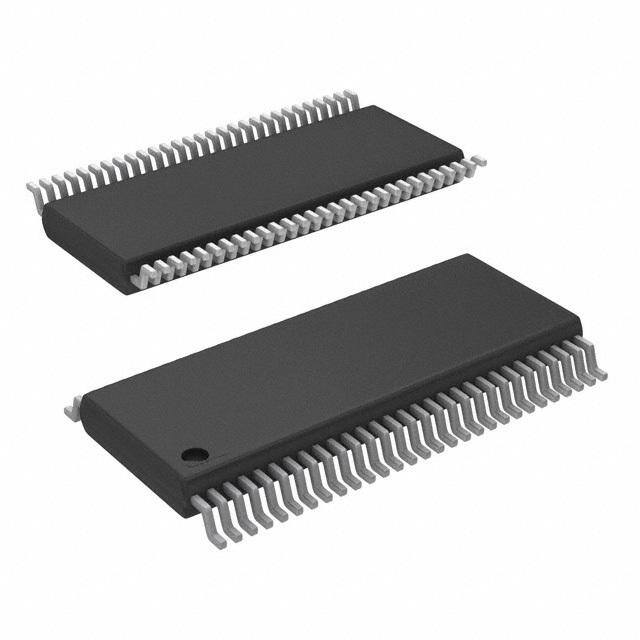
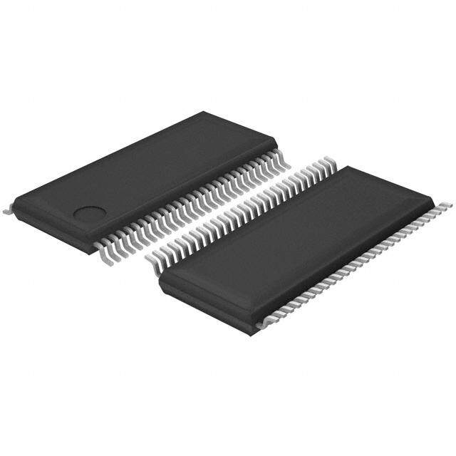
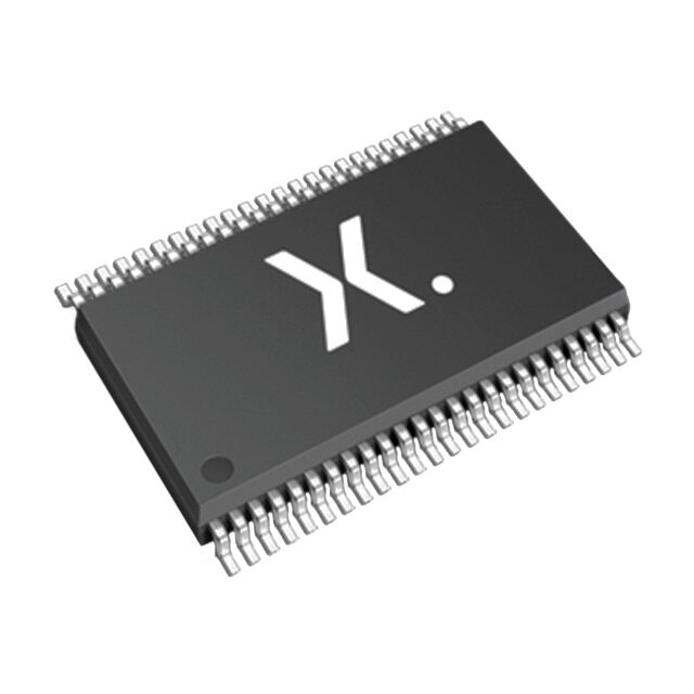
ICGOO电子元器件商城为您提供74AVC20T245DGVRG4由Texas Instruments设计生产,在icgoo商城现货销售,并且可以通过原厂、代理商等渠道进行代购。 74AVC20T245DGVRG4价格参考。Texas Instruments74AVC20T245DGVRG4封装/规格:逻辑器件 - 转换器,电平移位器, 双向 电压电平 转换器 2 电路 10 通道 380Mbps 56-TVSOP。您可以下载74AVC20T245DGVRG4参考资料、Datasheet数据手册功能说明书,资料中有74AVC20T245DGVRG4 详细功能的应用电路图电压和使用方法及教程。
74AVC20T245DGVRG4 是 Texas Instruments(德州仪器)生产的一款 20 位双电源电压电平移位器,属于逻辑器件中的电平转换器类别。该器件主要用于在不同电压域之间实现数据的双向传输。

其典型应用场景包括:

1. 多电压系统接口:在使用不同供电电压的数字电路之间进行信号转换,如将 1.2V 或 1.5V 的 FPGA、ASIC 或处理器接口与 3.3V 或 5V 外设连接。

2. 数据总线隔离与转换:适用于需要在两个不同电压域之间隔离并转换数据总线的应用,例如通信模块或嵌入式系统中。

3. 高性能计算设备:用于服务器、网络交换设备和存储系统中,以支持高速信号转换和增强系统兼容性。

4. 便携式电子产品:如智能手机和平板电脑中,用于低电压核心逻辑与较高电压外围设备之间的接口匹配。

该芯片具有宽电压范围(1.2V 至 3.6V)、高数据速率(可支持高达 210Mbps 的转换速度)以及低功耗特性,适合对性能和功耗都有要求的应用场景。
| 参数 | 数值 |
| 产品目录 | 集成电路 (IC)半导体 |
| 描述 | IC BUS TRANSCVR 20BIT 56TVSOP转换 - 电压电平 20B Dual Supply Bus Transceiver |
| 产品分类 | 逻辑 - 变换器集成电路 - IC |
| 品牌 | Texas Instruments |
| 产品手册 | |
| 产品图片 | |
| rohs | 符合RoHS无铅 / 符合限制有害物质指令(RoHS)规范要求 |
| 产品系列 | 逻辑集成电路,转换 - 电压电平,Texas Instruments 74AVC20T245DGVRG474AVC |
| 数据手册 | |
| 产品型号 | 74AVC20T245DGVRG4 |
| 产品种类 | 转换 - 电压电平 |
| 传播延迟时间 | 6.4 ns |
| 传播延迟(最大值) | 2.9ns |
| 位数 | 20 |
| 供应商器件封装 | 56-TVSOP |
| 包装 | 带卷 (TR) |
| 单位重量 | 145 mg |
| 商标 | Texas Instruments |
| 安装类型 | 表面贴装 |
| 安装风格 | SMD/SMT |
| 封装 | Reel |
| 封装/外壳 | 56-TFSOP(0.173",4.40mm 宽) |
| 封装/箱体 | TVSOP-56 |
| 工作温度 | -40°C ~ 85°C |
| 工厂包装数量 | 2000 |
| 差分-输入:输出 | 无/无 |
| 数据速率 | 380Mbps |
| 最大工作温度 | + 85 C |
| 最小工作温度 | - 40 C |
| 标准包装 | 2,000 |
| 电压-电源 | 1.2 V ~ 3.6 V |
| 电源电压-最大 | 3.6 V |
| 电源电压-最小 | 1.2 V |
| 系列 | SN74AVC20T245 |
| 输入类型 | 逻辑 |
| 输出/通道数 | 1 |
| 输出类型 | 3-State |
| 通道数 | 2 |
| 逻辑功能 | 变换器,双向,3 态 |


- 商务部:美国ITC正式对集成电路等产品启动337调查
- 曝三星4nm工艺存在良率问题 高通将骁龙8 Gen1或转产台积电
- 太阳诱电将投资9.5亿元在常州建新厂生产MLCC 预计2023年完工
- 英特尔发布欧洲新工厂建设计划 深化IDM 2.0 战略
- 台积电先进制程称霸业界 有大客户加持明年业绩稳了
- 达到5530亿美元!SIA预计今年全球半导体销售额将创下新高
- 英特尔拟将自动驾驶子公司Mobileye上市 估值或超500亿美元
- 三星加码芯片和SET,合并消费电子和移动部门,撤换高东真等 CEO
- 三星电子宣布重大人事变动 还合并消费电子和移动部门
- 海关总署:前11个月进口集成电路产品价值2.52万亿元 增长14.8%


PDF Datasheet 数据手册内容提取
(cid:1)(cid:2)(cid:3)(cid:4)(cid:5)(cid:6)(cid:7)(cid:8)(cid:9)(cid:10)(cid:8)(cid:4)(cid:11) (cid:8)(cid:9)(cid:12)(cid:13)(cid:14)(cid:10) (cid:15)(cid:16)(cid:5)(cid:17)(cid:12)(cid:1)(cid:16)(cid:18)(cid:18)(cid:17)(cid:19) (cid:13)(cid:16)(cid:1) (cid:10)(cid:20)(cid:5)(cid:2)(cid:1)(cid:7)(cid:21)(cid:14)(cid:6)(cid:21)(cid:20) (cid:22)(cid:14)(cid:10)(cid:23) (cid:7)(cid:24)(cid:2)(cid:25)(cid:14)(cid:26)(cid:16)(cid:20)(cid:5)(cid:13)(cid:17)(cid:21) (cid:6)(cid:24)(cid:17)(cid:10)(cid:5)(cid:26)(cid:21) (cid:10)(cid:20)(cid:5)(cid:2)(cid:1)(cid:17)(cid:5)(cid:10)(cid:14)(cid:24)(cid:2) (cid:5)(cid:2)(cid:15) (cid:27)(cid:12)(cid:1)(cid:10)(cid:5)(cid:10)(cid:21) (cid:24)(cid:16)(cid:10)(cid:18)(cid:16)(cid:10)(cid:1) SCES566F − MAY 2004 − REVISED APRIL 2005 (cid:1) Control Inputs V /V Levels are DGG OR DGV PACKAGE IH IL Referenced to V Voltage (TOP VIEW) CCA (cid:1) VCC Isolation Feature − If Either VCC Input 1DIR 1 56 1OE Is at GND, Both Ports Are in the 1B1 2 55 1A1 High-Impedance State 1B2 3 54 1A2 (cid:1) Overvoltage-Tolerant Inputs/Outputs Allow GND 4 53 GND Mixed-Voltage-Mode Data Communications 1B3 5 52 1A3 (cid:1) Fully Configurable Dual-Rail Design Allows 1B4 6 51 1A4 Each Port to Operate Over the Full 1.2-V to VCCB 7 50 VCCA 3.6-V Power-Supply Range 1B5 8 49 1A5 (cid:1) Ioff Supports Partial-Power-Down Mode 1B6 9 48 1A6 Operation 1B7 10 47 1A7 (cid:1) I/Os Are 4.6-V Tolerant GND 11 46 GND (cid:1) 1B8 12 45 1A8 Max Data Rates 1B9 13 44 1A9 − 380 Mbps (1.8-V to 3.3-V Translation) 1B10 14 43 1A10 − 260 Mbps (< 1.8-V to 3.3-V Translation) 2B1 15 42 2A1 − 260 Mbps (Translate to 2.5 V) 2B2 16 41 2A2 − 210 Mbps (Translate to 1.8 V) − 120 Mbps (Translate to 1.5 V) 2B3 17 40 2A3 − 100 Mbps (Translate to 1.2 V) GND 18 39 GND (cid:1) 2B4 19 38 2A4 Latch-Up Performance Exceeds 100 mA Per 2B5 20 37 2A5 JESD 78, Class II 2B6 21 36 2A6 (cid:1) ESD Protection Exceeds JESD 22 VCCB 22 35 VCCA − 8000-V Human-Body Model (A114-A) 2B7 23 34 2A7 − 200-V Machine Model (A115-A) 2B8 24 33 2A8 − 1000-V Charged-Device Model (C101) GND 25 32 GND 2B9 26 31 2A9 description/ordering information 2B10 27 30 2A10 This 20-bit noninverting bus transceiver uses two 2DIR 28 29 2OE separate configurable power-supply rails. The SN74AVC20T245 is optimized to operate with V /V set at 1.4 V to 3.6 V. It is operational with CCA CCB V /V as low as 1.2 V. The A port is designed to track V . V accepts any supply voltage from CCA CCB CCA CCA 1.2 V to 3.6 V. The B port is designed to track V . V accepts any supply voltage from 1.2 V to 3.6 V. This CCB CCB allows for universal low-voltage bidirectional translation between any of the 1.2-V, 1.5-V, 1.8-V, 2.5-V, and 3.3-V voltage nodes. ORDERING INFORMATION ORDERABLE TOP-SIDE TA PACKAGE† PART NUMBER MARKING TSSOP − DGG Tape and reel SN74AVC20T245DGGR AVC20T245 TVSOP − DGV Tape and reel SN74AVC20T245DGVR WG245 −−4400°°CC ttoo 8855°°CC VFBGA − GQL SN74AVC20T245GQLR TTaappee aanndd rreeeell WWGG224455 VFBGA − ZQL (Pb-free) SN74AVC20T245ZQLR †Package drawings, standard packing quantities, thermal data, symbolization, and PCB design guidelines are available at www.ti.com/sc/package. Please be aware that an important notice concerning availability, standard warranty, and use in critical applications of TexasInstruments semiconductor products and disclaimers thereto appears at the end of this data sheet. (cid:18)(cid:20)(cid:24)(cid:15)(cid:16)(cid:7)(cid:10)(cid:14)(cid:24)(cid:2) (cid:15)(cid:5)(cid:10)(cid:5) (cid:28)(cid:29)(cid:30)(cid:31)!"#$(cid:28)(cid:31)(cid:29) (cid:28)% &’!!((cid:29)$ #% (cid:31)(cid:30) )’*+(cid:28)&#$(cid:28)(cid:31)(cid:29) ,#$(- Copyright 2005, Texas Instruments Incorporated (cid:18)!(cid:31),’&$% &(cid:31)(cid:29)(cid:30)(cid:31)!" $(cid:31) %)(&(cid:28)(cid:30)(cid:28)&#$(cid:28)(cid:31)(cid:29)% )(! $.( $(!"% (cid:31)(cid:30) (cid:10)(/#% (cid:14)(cid:29)%$!’"((cid:29)$% %$#(cid:29),#!, 0#!!#(cid:29)$1- (cid:18)!(cid:31),’&$(cid:28)(cid:31)(cid:29) )!(cid:31)&(%%(cid:28)(cid:29)2 ,(cid:31)(% (cid:29)(cid:31)$ (cid:29)(&(%%#!(cid:28)+1 (cid:28)(cid:29)&+’,( $(%$(cid:28)(cid:29)2 (cid:31)(cid:30) #++ )#!#"($(!%- POST OFFICE BOX 655303 • DALLAS, TEXAS 75265 1
(cid:1)(cid:2)(cid:3)(cid:4)(cid:5)(cid:6)(cid:7)(cid:8)(cid:9)(cid:10)(cid:8)(cid:4)(cid:11) (cid:8)(cid:9)(cid:12)(cid:13)(cid:14)(cid:10) (cid:15)(cid:16)(cid:5)(cid:17)(cid:12)(cid:1)(cid:16)(cid:18)(cid:18)(cid:17)(cid:19) (cid:13)(cid:16)(cid:1) (cid:10)(cid:20)(cid:5)(cid:2)(cid:1)(cid:7)(cid:21)(cid:14)(cid:6)(cid:21)(cid:20) (cid:22)(cid:14)(cid:10)(cid:23) (cid:7)(cid:24)(cid:2)(cid:25)(cid:14)(cid:26)(cid:16)(cid:20)(cid:5)(cid:13)(cid:17)(cid:21) (cid:6)(cid:24)(cid:17)(cid:10)(cid:5)(cid:26)(cid:21) (cid:10)(cid:20)(cid:5)(cid:2)(cid:1)(cid:17)(cid:5)(cid:10)(cid:14)(cid:24)(cid:2) (cid:5)(cid:2)(cid:15) (cid:27)(cid:12)(cid:1)(cid:10)(cid:5)(cid:10)(cid:21) (cid:24)(cid:16)(cid:10)(cid:18)(cid:16)(cid:10)(cid:1) SCES566F − MAY 2004 − REVISED APRIL 2005 description/ordering information (continued) The SN74AVC20T245 is designed for asynchronous communication between data buses. The device transmits data from the A bus to the B bus or from the B bus to the A bus, depending on the logic level at the direction-control (DIR) input. The output-enable (OE) input is used to disable the outputs so that the buses are isolated. The SN74AVC20T245 is designed so that the control (1DIR, 2DIR, 1OE, and 2OE) inputs are supplied by V . CCA This device is fully specified for partial-power-down applications using I . The I circuitry disables the outputs, off off preventing damaging current backflow through the device when it is powered down. The V isolation feature ensures that if either V input is at GND, both ports are in the high-impedance state. CC CC To ensure the high-impedance state during power up or power down, OE should be tied to V through a pullup CC resistor; the minimum value of the resistor is determined by the current-sinking capability of the driver. GQL OR ZQL PACKAGE (TOP VIEW) terminal assignments 1 2 3 4 5 6 1 2 3 4 5 6 A 1B1 1B2 1DIR 1OE 1A2 1A1 A B 1B3 1B4 GND GND 1A4 1A3 B C C 1B5 1B6 VCCB VCCA 1A6 1A5 D 1B7 1B8 GND GND 1A8 1A7 D E 1B9 1B10 1A10 1A9 E F 2B1 2B2 2A2 2A1 F G 2B3 2B4 GND GND 2A4 2A3 G H 2B5 2B6 VCCB VCCA 2A6 2A5 H J 2B7 2B8 GND GND 2A8 2A7 J K 2B9 2B10 2DIR 2OE 2A10 2A9 K FUNCTION TABLE (each 10-bit section) INPUTS OOPPEERRAATTIIOONN OE DIR L L B data to A bus L H A data to B bus H X Isolation 2 POST OFFICE BOX 655303 • DALLAS, TEXAS 75265
(cid:1)(cid:2)(cid:3)(cid:4)(cid:5)(cid:6)(cid:7)(cid:8)(cid:9)(cid:10)(cid:8)(cid:4)(cid:11) (cid:8)(cid:9)(cid:12)(cid:13)(cid:14)(cid:10) (cid:15)(cid:16)(cid:5)(cid:17)(cid:12)(cid:1)(cid:16)(cid:18)(cid:18)(cid:17)(cid:19) (cid:13)(cid:16)(cid:1) (cid:10)(cid:20)(cid:5)(cid:2)(cid:1)(cid:7)(cid:21)(cid:14)(cid:6)(cid:21)(cid:20) (cid:22)(cid:14)(cid:10)(cid:23) (cid:7)(cid:24)(cid:2)(cid:25)(cid:14)(cid:26)(cid:16)(cid:20)(cid:5)(cid:13)(cid:17)(cid:21) (cid:6)(cid:24)(cid:17)(cid:10)(cid:5)(cid:26)(cid:21) (cid:10)(cid:20)(cid:5)(cid:2)(cid:1)(cid:17)(cid:5)(cid:10)(cid:14)(cid:24)(cid:2) (cid:5)(cid:2)(cid:15) (cid:27)(cid:12)(cid:1)(cid:10)(cid:5)(cid:10)(cid:21) (cid:24)(cid:16)(cid:10)(cid:18)(cid:16)(cid:10)(cid:1) SCES566F − MAY 2004 − REVISED APRIL 2005 logic diagram (positive logic) 1 28 1DIR 2DIR 56 29 1OE 2OE 55 42 1A1 2A1 2 15 1B1 2B1 To Nine Other Channels To Nine Other Channels Pin numbers shown are for the DGG and DGV packages. absolute maximum ratings over operating free-air temperature range (unless otherwise noted)† Supply voltage range, V and V . . . . . . . . . . . . . . . . . . . . . . . . . . . . . . . . . . . . . . . . . . . . . . −0.5 V to 4.6 V CCA CCB Input voltage range, V (see Note 1): I/O ports (A port) . . . . . . . . . . . . . . . . . . . . . . . . . . . . . . . . . −0.5 V to 4.6 V I I/O ports (B port) . . . . . . . . . . . . . . . . . . . . . . . . . . . . . . . . . −0.5 V to 4.6 V Control inputs . . . . . . . . . . . . . . . . . . . . . . . . . . . . . . . . . . . −0.5 V to 4.6 V Voltage range applied to any output in the high-impedance or power-off state, V O (see Note 1): (A port) . . . . . . . . . . . . . . . . . . . . . . . . . . . . . . . . . . . . . . . . . . . . . . . . . . . . . . . . . . . −0.5 V to 4.6 V (B port) . . . . . . . . . . . . . . . . . . . . . . . . . . . . . . . . . . . . . . . . . . . . . . . . . . . . . . . . . . . −0.5 V to 4.6 V Voltage range applied to any output in the high or low state, V O (see Notes 1 and 2): (A port) . . . . . . . . . . . . . . . . . . . . . . . . . . . . . . . . . . . . . . . . . . . . −0.5 V to V + 0.5 V CCA (B port) . . . . . . . . . . . . . . . . . . . . . . . . . . . . . . . . . . . . . . . . . . . . −0.5 V to V + 0.5 V CCB Input clamp current, I (V < 0) . . . . . . . . . . . . . . . . . . . . . . . . . . . . . . . . . . . . . . . . . . . . . . . . . . . . . . . . . . . −50 mA IK I Output clamp current, I (V < 0) . . . . . . . . . . . . . . . . . . . . . . . . . . . . . . . . . . . . . . . . . . . . . . . . . . . . . . . . −50 mA OK O Continuous output current, I . . . . . . . . . . . . . . . . . . . . . . . . . . . . . . . . . . . . . . . . . . . . . . . . . . . . . . . . . . . . . ±50 mA O Continuous current through each V , V , and GND . . . . . . . . . . . . . . . . . . . . . . . . . . . . . . . . . . . ±100 mA CCA CCB Package thermal impedance, θJA (see Note 3): DGG package . . . . . . . . . . . . . . . . . . . . . . . . . . . . . . . 64°C/W DGV package . . . . . . . . . . . . . . . . . . . . . . . . . . . . . . . . 48°C/W GQL/ZQL package . . . . . . . . . . . . . . . . . . . . . . . . . . . 42°C/W Storage temperature range, T . . . . . . . . . . . . . . . . . . . . . . . . . . . . . . . . . . . . . . . . . . . . . . . . . . . −65°C to 150°C stg †Stresses beyond those listed under “absolute maximum ratings” may cause permanent damage to the device. These are stress ratings only, and functional operation of the device at these or any other conditions beyond those indicated under “recommended operating conditions” is not implied. Exposure to absolute-maximum-rated conditions for extended periods may affect device reliability. NOTES: 1. The input voltage and output negative-voltage ratings may be exceeded if the input and output current ratings are observed. 2. The output positive-voltage rating may be exceeded up to 4.6 V maximum if the output current rating is observed. 3. The package thermal impedance is calculated in accordance with JESD 51-7. POST OFFICE BOX 655303 • DALLAS, TEXAS 75265 3
(cid:1)(cid:2)(cid:3)(cid:4)(cid:5)(cid:6)(cid:7)(cid:8)(cid:9)(cid:10)(cid:8)(cid:4)(cid:11) (cid:8)(cid:9)(cid:12)(cid:13)(cid:14)(cid:10) (cid:15)(cid:16)(cid:5)(cid:17)(cid:12)(cid:1)(cid:16)(cid:18)(cid:18)(cid:17)(cid:19) (cid:13)(cid:16)(cid:1) (cid:10)(cid:20)(cid:5)(cid:2)(cid:1)(cid:7)(cid:21)(cid:14)(cid:6)(cid:21)(cid:20) (cid:22)(cid:14)(cid:10)(cid:23) (cid:7)(cid:24)(cid:2)(cid:25)(cid:14)(cid:26)(cid:16)(cid:20)(cid:5)(cid:13)(cid:17)(cid:21) (cid:6)(cid:24)(cid:17)(cid:10)(cid:5)(cid:26)(cid:21) (cid:10)(cid:20)(cid:5)(cid:2)(cid:1)(cid:17)(cid:5)(cid:10)(cid:14)(cid:24)(cid:2) (cid:5)(cid:2)(cid:15) (cid:27)(cid:12)(cid:1)(cid:10)(cid:5)(cid:10)(cid:21) (cid:24)(cid:16)(cid:10)(cid:18)(cid:16)(cid:10)(cid:1) SCES566F − MAY 2004 − REVISED APRIL 2005 recommended operating conditions (see Notes 4 through 8) VCCI VCCO MIN MAX UNIT VCCA Supply voltage 1.2 3.6 V VCCB Supply voltage 1.2 3.6 V 1.2 V to 1.95 V VCCI ×0.65 HHiigghh--lleevveell iinnppuutt DDaattaa iinnppuuttss VVIIHH vvoollttaaggee ((sseeee NNoottee 77)) 1.95 V to 2.7 V 1.6 VV 2.7 V to 3.6 V 2 1.2 V to 1.95 V VCCI ×0.35 LLooww--lleevveell iinnppuutt DDaattaa iinnppuuttss VVIILL vvoollttaaggee ((sseeee NNoottee 77)) 1.95 V to 2.7 V 0.7 VV 2.7 V to 3.6 V 0.8 1.2 V to 1.95 V VCCA ×0.65 DDIIRR HHiigghh--lleevveell iinnppuutt VVIIHH vvoollttaaggee ((rreeffeerreenncceedd ttoo VVCCCCAA)) 1.95 V to 2.7 V 1.6 VV (see Note 8) 2.7 V to 3.6 V 2 1.2 V to 1.95 V VCCA ×0.35 DDIIRR LLooww--lleevveell iinnppuutt VVIILL vvoollttaaggee ((rreeffeerreenncceedd ttoo VVCCCCAA)) 1.95 V to 2.7 V 0.7 VV (see Note 8) 2.7 V to 3.6 V 0.8 VI Input voltage 0 3.6 V Active state 0 VCCO VVOO OOuuttppuutt vvoollttaaggee VV 3-state 0 3.6 1.2 V −3 1.4 V to 1.6 V −6 IIOOHH HHiigghh--lleevveell oouuttppuutt ccuurrrreenntt 1.65 V to 1.95 V −8 mmAA 2.3 V to 2.7 V −9 3 V to 3.6 V −12 1.2 V 3 1.4 V to 1.6 V 6 IIOOLL LLooww--lleevveell oouuttppuutt ccuurrrreenntt 1.65 V to 1.95 V 8 mmAA 2.3 V to 2.7 V 9 3 V to 3.6 V 12 ∆t/∆v Input transition rise or fall rate 5 ns/V TA Operating free-air temperature −40 85 °C NOTES: 4. VCCI is the VCC associated with the data input port. 5. VCCO is the VCC associated with the output port. 6. All unused data inputs of the device must be held at VCCI or GND to ensure proper device operation. Refer to the TI application report, Implications of Slow or Floating CMOS Inputs, literature number SCBA004. 7. For VCCI values not specified in the data sheet, VIH(min) = VCCI x 0.7 V, VIL(max) = VCCI x 0.3 V. 8. For VCCI values not specified in the data sheet, VIH(min) = VCCA x 0.7 V, VIL(max) = VCCA x 0.3 V. 4 POST OFFICE BOX 655303 • DALLAS, TEXAS 75265
(cid:1)(cid:2)(cid:3)(cid:4)(cid:5)(cid:6)(cid:7)(cid:8)(cid:9)(cid:10)(cid:8)(cid:4)(cid:11) (cid:8)(cid:9)(cid:12)(cid:13)(cid:14)(cid:10) (cid:15)(cid:16)(cid:5)(cid:17)(cid:12)(cid:1)(cid:16)(cid:18)(cid:18)(cid:17)(cid:19) (cid:13)(cid:16)(cid:1) (cid:10)(cid:20)(cid:5)(cid:2)(cid:1)(cid:7)(cid:21)(cid:14)(cid:6)(cid:21)(cid:20) (cid:22)(cid:14)(cid:10)(cid:23) (cid:7)(cid:24)(cid:2)(cid:25)(cid:14)(cid:26)(cid:16)(cid:20)(cid:5)(cid:13)(cid:17)(cid:21) (cid:6)(cid:24)(cid:17)(cid:10)(cid:5)(cid:26)(cid:21) (cid:10)(cid:20)(cid:5)(cid:2)(cid:1)(cid:17)(cid:5)(cid:10)(cid:14)(cid:24)(cid:2) (cid:5)(cid:2)(cid:15) (cid:27)(cid:12)(cid:1)(cid:10)(cid:5)(cid:10)(cid:21) (cid:24)(cid:16)(cid:10)(cid:18)(cid:16)(cid:10)(cid:1) SCES566F − MAY 2004 − REVISED APRIL 2005 electrical characteristics over recommended operating free-air temperature range (unless otherwise noted) (see Notes 9 and 10) TA = 25°C −40°C to 85°C PPAARRAAMMEETTEERR TTEESSTT CCOONNDDIITTIIOONNSS VVCCCCAA VVCCCCBB UUNNIITT MIN TYP MAX MIN MAX IOH = −100 µA 1.2 V to 3.6 V 1.2 V to 3.6 V VCCO − 0.2 V IOH = −3 mA 1.2 V 1.2 V 0.95 IOH = −6 mA 1.4 V 1.4 V 1.05 VVOOHH VVII == VVIIHH VV IOH = −8 mA 1.65 V 1.65 V 1.2 IOH = −9 mA 2.3 V 2.3 V 1.75 IOH = −12 mA 3 V 3 V 2.3 IOL = 100 µA 1.2 V to 3.6 V 1.2 V to 3.6 V 0.2 IOL = 3 mA 1.2 V 1.2 V 0.15 IOL = 6 mA 1.4 V 1.4 V 0.35 VVOOLL VVII == VVIILL VV IOL = 8 mA 1.65 V 1.65 V 0.45 IOL = 9 mA 2.3 V 2.3 V 0.55 IOL = 12 mA 3 V 3 V 0.7 Control II inputs VI = VCCA or GND 1.2 V to 3.6 V 1.2 V to 3.6 V ±0.025 ±0.25 ±1 µA A or B 0 V 0 to 3.6 V ±0.1 ±1 ±5 port IIooffff VVII oorr VVOO == 00 ttoo 33..66 VV µAA A or B 0 to 3.6 V 0 V ±0.1 ±1 ±5 port VO = VCCO or IOZ† A or B GND, OE = VIH 3.6 V 3.6 V ±0.5 ±2.5 ±5 µA ports VI = VCCI or GND 1.2 V to 3.6 V 1.2 V to 3.6 V 35 IICCCCAA VVII == VVCCCCII oorr GGNNDD,, IIOO == 00 0 V 3.6 V −5 µµAA 3.6 V 0 V 35 1.2 V to 3.6 V 1.2 V to 3.6 V 35 IICCCCBB VVII == VVCCCCII oorr GGNNDD,, IIOO == 00 0 V 3.6 V 35 µµAA 3.6 V 0 V −5 ICCA(cid:1)ICCB VI = VCCI or GND, IO = 0 1.2 V to 3.6 V 1.2 V to 3.6 V 65 µA Control Ci inputs VI = 3.3 V or GND 3.3 V 3.3 V 3.5 pF A or B Cio ports VO = 3.3 V or GND 3.3 V 3.3 V 7 pF †For I/O ports, the parameter IOZ includes the input leakage current. NOTES: 9. VCCO is the VCC associated with the output port. 10. VCCI is the VCC associated with the input port. POST OFFICE BOX 655303 • DALLAS, TEXAS 75265 5
(cid:1)(cid:2)(cid:3)(cid:4)(cid:5)(cid:6)(cid:7)(cid:8)(cid:9)(cid:10)(cid:8)(cid:4)(cid:11) (cid:8)(cid:9)(cid:12)(cid:13)(cid:14)(cid:10) (cid:15)(cid:16)(cid:5)(cid:17)(cid:12)(cid:1)(cid:16)(cid:18)(cid:18)(cid:17)(cid:19) (cid:13)(cid:16)(cid:1) (cid:10)(cid:20)(cid:5)(cid:2)(cid:1)(cid:7)(cid:21)(cid:14)(cid:6)(cid:21)(cid:20) (cid:22)(cid:14)(cid:10)(cid:23) (cid:7)(cid:24)(cid:2)(cid:25)(cid:14)(cid:26)(cid:16)(cid:20)(cid:5)(cid:13)(cid:17)(cid:21) (cid:6)(cid:24)(cid:17)(cid:10)(cid:5)(cid:26)(cid:21) (cid:10)(cid:20)(cid:5)(cid:2)(cid:1)(cid:17)(cid:5)(cid:10)(cid:14)(cid:24)(cid:2) (cid:5)(cid:2)(cid:15) (cid:27)(cid:12)(cid:1)(cid:10)(cid:5)(cid:10)(cid:21) (cid:24)(cid:16)(cid:10)(cid:18)(cid:16)(cid:10)(cid:1) SCES566F − MAY 2004 − REVISED APRIL 2005 switching characteristics over recommended operating free-air temperature range, VCCA = 1.2 V (see Figure 1) FFRROOMM TTOO VCCB = 1.2 V VCCB = 1.5 V VCCB = 1.8 V VCCB = 2.5 V VCCB = 3.3 V PPAARRAAMMEETTEERR UUNNIITT (INPUT) (OUTPUT) TYP TYP TYP TYP TYP tPLH 3.8 3.1 2.8 2.7 3.3 AA BB nnss tPHL 3.8 3.1 2.8 2.7 3.3 tPLH 4.1 3.8 3.6 3.5 3.4 BB AA nnss tPHL 4.1 3.8 3.6 3.5 3.4 tPZH 6.5 6.5 6.5 6.5 6.5 OOEE AA nnss tPZL 6.5 6.5 6.5 6.5 6.5 tPZH 5.6 4.4 3.8 3.3 3.2 OOEE BB nnss tPZL 5.6 4.4 3.8 3.3 3.2 tPHZ 6.4 6.4 6.4 6.4 6.4 OOEE AA nnss tPLZ 6.4 6.4 6.4 6.4 6.4 tPHZ 5.7 4.6 4.7 4.1 5.4 OOEE BB nnss tPLZ 5.7 4.6 4.7 4.1 5.4 switching characteristics over recommended operating free-air temperature range, VCCA = 1.5 V ± 0.1 V (see Figure 1) VCCB = 1.5 V VCCB = 1.8 V VCCB = 2.5 V VCCB = 3.3 V PPAARRAAMMEETTEERR FROM TO VCCB = 1.2 V ± 0.1 V ± 0.15 V ± 0.2 V ± 0.3 V UUNNIITT ((IINNPPUUTT)) ((OOUUTTPPUUTT)) TYP MIN MAX MIN MAX MIN MAX MIN MAX tPLH 3.8 0.5 6.4 0.5 5.4 0.5 4.3 0.5 3.9 AA BB nnss tPHL 3.8 0.5 6.4 0.5 5.4 0.5 4.3 0.5 3.9 tPLH 3.1 0.5 6.4 0.5 6.1 0.5 5.8 0.5 5.7 BB AA nnss tPHL 3.1 0.5 6.4 0.5 6.1 0.5 5.8 0.5 5.7 tPZH 4.3 1.5 10.3 1.5 10.3 1.5 10.2 1.5 10.2 OOEE AA nnss tPZL 4.3 1.5 10.3 1.5 10.3 1.5 10.2 1.5 10.2 tPZH 5.2 1 10.3 1 8.4 0.5 6.1 0.5 5.3 OOEE BB nnss tPZL 5.2 1 10.3 1 8.4 0.5 6.1 0.5 5.3 tPHZ 4.5 2 9 2 9 2 9 2 9 OOEE AA nnss tPLZ 4.5 2 9 2 9 2 9 2 9 tPHZ 5.1 1.5 9 1.5 7.8 1 6.4 1 5.9 OOEE BB nnss tPLZ 5.1 1.5 9 1.5 7.8 1 6.4 1 5.9 6 POST OFFICE BOX 655303 • DALLAS, TEXAS 75265
(cid:1)(cid:2)(cid:3)(cid:4)(cid:5)(cid:6)(cid:7)(cid:8)(cid:9)(cid:10)(cid:8)(cid:4)(cid:11) (cid:8)(cid:9)(cid:12)(cid:13)(cid:14)(cid:10) (cid:15)(cid:16)(cid:5)(cid:17)(cid:12)(cid:1)(cid:16)(cid:18)(cid:18)(cid:17)(cid:19) (cid:13)(cid:16)(cid:1) (cid:10)(cid:20)(cid:5)(cid:2)(cid:1)(cid:7)(cid:21)(cid:14)(cid:6)(cid:21)(cid:20) (cid:22)(cid:14)(cid:10)(cid:23) (cid:7)(cid:24)(cid:2)(cid:25)(cid:14)(cid:26)(cid:16)(cid:20)(cid:5)(cid:13)(cid:17)(cid:21) (cid:6)(cid:24)(cid:17)(cid:10)(cid:5)(cid:26)(cid:21) (cid:10)(cid:20)(cid:5)(cid:2)(cid:1)(cid:17)(cid:5)(cid:10)(cid:14)(cid:24)(cid:2) (cid:5)(cid:2)(cid:15) (cid:27)(cid:12)(cid:1)(cid:10)(cid:5)(cid:10)(cid:21) (cid:24)(cid:16)(cid:10)(cid:18)(cid:16)(cid:10)(cid:1) SCES566F − MAY 2004 − REVISED APRIL 2005 switching characteristics over recommended operating free-air temperature range, VCCA = 1.8 V ± 0.15 V (see Figure 1) VCCB = 1.5 V VCCB = 1.8 V VCCB = 2.5 V VCCB = 3.3 V PPAARRAAMMEETTEERR FROM TO VCCB = 1.2 V ± 0.1 V ± 0.15 V ± 0.2 V ± 0.3 V UUNNIITT ((IINNPPUUTT)) ((OOUUTTPPUUTT)) TYP MIN MAX MIN MAX MIN MAX MIN MAX tPLH 3.6 0.5 6.1 0.5 5 0.5 3.9 0.5 3.5 AA BB nnss tPHL 3.6 0.5 6.1 0.5 5 0.5 3.9 0.5 3.5 tPLH 2.8 0.5 5.4 0.5 5 0.5 4.7 0.5 4.6 BB AA nnss tPHL 2.8 0.5 5.4 0.5 5 0.5 4.7 0.5 4.6 tPZH 3.4 1 8.1 1 7.9 1 7.9 1 7.9 OOEE AA nnss tPZL 3.4 1 8.1 1 7.9 1 7.9 1 7.9 tPZH 5 0.5 10 0.5 7.9 0.5 5.7 0.5 4.8 OOEE BB nnss tPZL 5 0.5 10 0.5 7.9 0.5 5.7 0.5 4.8 tPHZ 4.1 2 7.4 2 7.4 2 7.4 2 7.4 OOEE AA nnss tPLZ 4.1 2 7.4 2 7.4 2 7.4 2 7.4 tPHZ 4.9 1.5 8.7 1.5 7.4 1 5.8 1 5.1 OOEE BB nnss tPLZ 4.9 1.5 8.7 1.5 7.4 1 5.8 1 5.1 switching characteristics over recommended operating free-air temperature range, VCCA = 2.5 V ± 0.2 V (see Figure 1) VCCB = 1.5 V VCCB = 1.8 V VCCB = 2.5 V VCCB = 3.3 V PPAARRAAMMEETTEERR FROM TO VCCB = 1.2 V ± 0.1 V ± 0.15 V ± 0.2 V ± 0.3 V UUNNIITT ((IINNPPUUTT)) ((OOUUTTPPUUTT)) TYP MIN MAX MIN MAX MIN MAX MIN MAX tPLH 3.5 0.5 5.8 0.5 4.7 0.5 3.5 0.5 3 AA BB nnss tPHL 3.5 0.5 5.8 0.5 4.7 0.5 3.5 0.5 3 tPLH 2.7 0.5 4.3 0.5 3.9 0.5 3.5 0.5 3.4 BB AA nnss tPHL 2.7 0.5 4.3 0.5 3.9 0.5 3.5 0.5 3.4 tPZH 2.5 0.5 5.4 0.5 5.3 0.5 5.2 0.5 5.2 OOEE AA nnss tPZL 2.5 0.5 5.4 0.5 5.3 0.5 5.2 0.5 5.2 tPZH 4.8 0.5 9.6 0.5 7.6 0.5 5.3 0.5 4.3 OOEE BB nnss tPZL 4.8 0.5 9.6 0.5 7.6 0.5 5.3 0.5 4.3 tPHZ 3 1.1 5.2 1.1 5.2 1.1 5.2 1.1 5.2 OOEE AA nnss tPLZ 3 1.1 5.2 1.1 5.2 1.1 5.2 1.1 5.2 tPHZ 4.7 1.2 8.2 1.2 6.9 1 5.3 1 5 OOEE BB nnss tPLZ 4.7 1.2 8.2 1.2 6.9 1 5.3 1 5 POST OFFICE BOX 655303 • DALLAS, TEXAS 75265 7
(cid:1)(cid:2)(cid:3)(cid:4)(cid:5)(cid:6)(cid:7)(cid:8)(cid:9)(cid:10)(cid:8)(cid:4)(cid:11) (cid:8)(cid:9)(cid:12)(cid:13)(cid:14)(cid:10) (cid:15)(cid:16)(cid:5)(cid:17)(cid:12)(cid:1)(cid:16)(cid:18)(cid:18)(cid:17)(cid:19) (cid:13)(cid:16)(cid:1) (cid:10)(cid:20)(cid:5)(cid:2)(cid:1)(cid:7)(cid:21)(cid:14)(cid:6)(cid:21)(cid:20) (cid:22)(cid:14)(cid:10)(cid:23) (cid:7)(cid:24)(cid:2)(cid:25)(cid:14)(cid:26)(cid:16)(cid:20)(cid:5)(cid:13)(cid:17)(cid:21) (cid:6)(cid:24)(cid:17)(cid:10)(cid:5)(cid:26)(cid:21) (cid:10)(cid:20)(cid:5)(cid:2)(cid:1)(cid:17)(cid:5)(cid:10)(cid:14)(cid:24)(cid:2) (cid:5)(cid:2)(cid:15) (cid:27)(cid:12)(cid:1)(cid:10)(cid:5)(cid:10)(cid:21) (cid:24)(cid:16)(cid:10)(cid:18)(cid:16)(cid:10)(cid:1) SCES566F − MAY 2004 − REVISED APRIL 2005 switching characteristics over recommended operating free-air temperature range, VCCA = 3.3 V ± 0.3 V (see Figure 1) VCCB = 1.5 V VCCB = 1.8 V VCCB = 2.5 V VCCB = 3.3 V PPAARRAAMMEETTEERR FROM TO VCCB = 1.2 V ± 0.1 V ± 0.15 V ± 0.2 V ± 0.3 V UUNNIITT ((IINNPPUUTT)) ((OOUUTTPPUUTT)) TYP MIN MAX MIN MAX MIN MAX MIN MAX tPLH 3.4 0.5 5.7 0.5 4.6 0.5 3.4 0.5 2.9 AA BB nnss tPHL 3.4 0.5 5.7 0.5 4.6 0.5 3.4 0.5 2.9 tPLH 3.3 0.5 3.9 0.5 3.5 0.5 3 0.5 2.9 BB AA nnss tPHL 3.3 0.5 3.9 0.5 3.5 0.5 3 0.5 2.9 tPZH 2.2 0.5 4.4 0.5 4.3 0.5 4.2 0.5 4.1 OOEE AA nnss tPZL 2.2 0.5 4.4 0.5 4.3 0.5 4.2 0.5 4.1 tPZH 4.7 1 9.6 0.5 7.5 0.5 5.1 0.5 4.1 OOEE BB nnss tPZL 4.7 1 9.6 0.5 7.5 0.5 5.1 0.5 4.1 tPHZ 3.4 0.8 5 0.8 5 0.8 5 0.8 5 OOEE AA nnss tPLZ 3.4 0.8 5 0.8 5 0.8 5 0.8 5 tPHZ 4.6 1.2 8.1 1.2 6.7 1 5.1 0.8 5 OOEE BB nnss tPLZ 4.6 1.2 8.1 1.2 6.7 1 5.1 0.8 5 operating characteristics, TA = 25°C VCCA = VCCA = VCCA = VCCA = VCCA = PPAARRAAMMEETTEERR TEST VCCB = 1.2 V VCCB = 1.5 V VCCB = 1.8 V VCCB = 2.5 V VCCB = 3.3 V UUNNIITT CCOONNDDIITTIIOONNSS TYP TYP TYP TYP TYP Outputs 1 1 1 1 2 Enabled AA ttoo BB Outputs Disabled CL = 0, 1 1 1 1 1 CCppddAA†† ff == 1100 MMHHzz,, ppFF Outputs tr = tf =1 ns 12 13 14 15 16 Enabled BB ttoo AA Outputs 1 1 1 1 1 Disabled Outputs 13 13 14 15 16 Enabled AA ttoo BB Outputs 1 1 1 1 1 Disabled CLL = 0, CCppddBB†† ff == 1100 MMHHzz,, ppFF Outputs tr = tf =1 ns 1 1 1 2 2 Enabled BB ttoo AA Outputs 1 1 1 1 1 Disabled †Power-dissipation capacitance per transceiver 8 POST OFFICE BOX 655303 • DALLAS, TEXAS 75265
(cid:1)(cid:2)(cid:3)(cid:4)(cid:5)(cid:6)(cid:7)(cid:8)(cid:9)(cid:10)(cid:8)(cid:4)(cid:11) (cid:8)(cid:9)(cid:12)(cid:13)(cid:14)(cid:10) (cid:15)(cid:16)(cid:5)(cid:17)(cid:12)(cid:1)(cid:16)(cid:18)(cid:18)(cid:17)(cid:19) (cid:13)(cid:16)(cid:1) (cid:10)(cid:20)(cid:5)(cid:2)(cid:1)(cid:7)(cid:21)(cid:14)(cid:6)(cid:21)(cid:20) (cid:22)(cid:14)(cid:10)(cid:23) (cid:7)(cid:24)(cid:2)(cid:25)(cid:14)(cid:26)(cid:16)(cid:20)(cid:5)(cid:13)(cid:17)(cid:21) (cid:6)(cid:24)(cid:17)(cid:10)(cid:5)(cid:26)(cid:21) (cid:10)(cid:20)(cid:5)(cid:2)(cid:1)(cid:17)(cid:5)(cid:10)(cid:14)(cid:24)(cid:2) (cid:5)(cid:2)(cid:15) (cid:27)(cid:12)(cid:1)(cid:10)(cid:5)(cid:10)(cid:21) (cid:24)(cid:16)(cid:10)(cid:18)(cid:16)(cid:10)(cid:1) SCES566F − MAY 2004 − REVISED APRIL 2005 typical total static power consumption (I + I ) CCA CCB TABLE 1 VCCA VVCCCCBB UUNNIITT 0 V 1.2 V 1.5 V 1.8 V 2.5 V 3.3 V 0 V 0 < 0.5 < 0.5 < 0.5 < 0.5 < 0.5 1.2 V < 0.5 < 1 < 1 < 1 < 1 1 1.5 V < 0.5 < 1 < 1 < 1 < 1 1 µAA 1.8 V < 0.5 < 1 < 1 < 1 < 1 < 1 2.5 V < 0.5 1 < 1 < 1 < 1 < 1 3.3 V < 0.5 1 < 1 < 1 < 1 < 1 POST OFFICE BOX 655303 • DALLAS, TEXAS 75265 9
(cid:1)(cid:2)(cid:3)(cid:4)(cid:5)(cid:6)(cid:7)(cid:8)(cid:9)(cid:10)(cid:8)(cid:4)(cid:11) (cid:8)(cid:9)(cid:12)(cid:13)(cid:14)(cid:10) (cid:15)(cid:16)(cid:5)(cid:17)(cid:12)(cid:1)(cid:16)(cid:18)(cid:18)(cid:17)(cid:19) (cid:13)(cid:16)(cid:1) (cid:10)(cid:20)(cid:5)(cid:2)(cid:1)(cid:7)(cid:21)(cid:14)(cid:6)(cid:21)(cid:20) (cid:22)(cid:14)(cid:10)(cid:23) (cid:7)(cid:24)(cid:2)(cid:25)(cid:14)(cid:26)(cid:16)(cid:20)(cid:5)(cid:13)(cid:17)(cid:21) (cid:6)(cid:24)(cid:17)(cid:10)(cid:5)(cid:26)(cid:21) (cid:10)(cid:20)(cid:5)(cid:2)(cid:1)(cid:17)(cid:5)(cid:10)(cid:14)(cid:24)(cid:2) (cid:5)(cid:2)(cid:15) (cid:27)(cid:12)(cid:1)(cid:10)(cid:5)(cid:10)(cid:21) (cid:24)(cid:16)(cid:10)(cid:18)(cid:16)(cid:10)(cid:1) SCES566F − MAY 2004 − REVISED APRIL 2005 TYPICAL CHARACTERISTICS TYPICAL PROPAGATION DELAY (A to B) vs LOAD CAPACITANCE TA = 25°C, VCCA = 1.2 V 6 6 5 5 4 4 − nsH 3 − nsL 3 L H tP tP 2 2 VCCB = 1.2 V VCCB = 1.2 V VCCB = 1.5 V VCCB = 1.5 V 1 VCCB = 1.8 V 1 VCCB = 1.8 V VCCB = 2.5 V VCCB = 2.5 V VCCB = 3.3 V VCCB = 3.3 V 0 0 0 10 20 30 40 50 60 0 10 20 30 40 50 60 CL − pF CL − pF Figure 1 Figure 2 TYPICAL PROPAGATION DELAY (A to B) vs LOAD CAPACITANCE TA = 25°C, VCCA = 1.5 V 6 6 5 5 4 4 − nsH 3 − nsL 3 L H tP tP 2 2 VCCB = 1.2 V VCCB = 1.2 V VCCB = 1.5 V VCCB = 1.5 V 1 VCCB = 1.8 V 1 VCCB = 1.8 V VCCB = 2.5 V VCCB = 2.5 V VCCB = 3.3 V VCCB = 3.3 V 0 0 0 10 20 30 40 50 60 0 10 20 30 40 50 60 CL − pF CL − pF Figure 3 Figure 4 10 POST OFFICE BOX 655303 • DALLAS, TEXAS 75265
(cid:1)(cid:2)(cid:3)(cid:4)(cid:5)(cid:6)(cid:7)(cid:8)(cid:9)(cid:10)(cid:8)(cid:4)(cid:11) (cid:8)(cid:9)(cid:12)(cid:13)(cid:14)(cid:10) (cid:15)(cid:16)(cid:5)(cid:17)(cid:12)(cid:1)(cid:16)(cid:18)(cid:18)(cid:17)(cid:19) (cid:13)(cid:16)(cid:1) (cid:10)(cid:20)(cid:5)(cid:2)(cid:1)(cid:7)(cid:21)(cid:14)(cid:6)(cid:21)(cid:20) (cid:22)(cid:14)(cid:10)(cid:23) (cid:7)(cid:24)(cid:2)(cid:25)(cid:14)(cid:26)(cid:16)(cid:20)(cid:5)(cid:13)(cid:17)(cid:21) (cid:6)(cid:24)(cid:17)(cid:10)(cid:5)(cid:26)(cid:21) (cid:10)(cid:20)(cid:5)(cid:2)(cid:1)(cid:17)(cid:5)(cid:10)(cid:14)(cid:24)(cid:2) (cid:5)(cid:2)(cid:15) (cid:27)(cid:12)(cid:1)(cid:10)(cid:5)(cid:10)(cid:21) (cid:24)(cid:16)(cid:10)(cid:18)(cid:16)(cid:10)(cid:1) SCES566F − MAY 2004 − REVISED APRIL 2005 TYPICAL PROPAGATION DELAY (A to B) vs LOAD CAPACITANCE TA = 25°C, VCCA = 1.8 V 6 6 5 5 4 4 − nsH 3 − nsL 3 L H tP tP 2 2 VCCB = 1.2 V VCCB = 1.2 V VCCB = 1.5 V VCCB = 1.5 V 1 VCCB = 1.8 V 1 VCCB = 1.8 V VCCB = 2.5 V VCCB = 2.5 V VCCB = 3.3 V VCCB = 3.3 V 0 0 0 10 20 30 40 50 60 0 10 20 30 40 50 60 CL − pF CL − pF Figure 5 Figure 6 TYPICAL PROPAGATION DELAY (A to B) vs LOAD CAPACITANCE TA = 25°C, VCCA = 2.5 V 6 6 VCCB = 1.2 V VCCB = 1.5 V 5 5 VCCB = 1.8 V VCCB = 2.5 V VCCB = 3.3 V 4 4 − nsH 3 − nsL 3 L H tP tP 2 2 VCCB = 1.2 V VCCB = 1.5 V 1 VCCB = 1.8 V 1 VCCB = 2.5 V VCCB = 3.3 V 0 0 0 10 20 30 40 50 60 0 10 20 30 40 50 60 CL − pF CL − pF Figure 7 Figure 8 POST OFFICE BOX 655303 • DALLAS, TEXAS 75265 11
(cid:1)(cid:2)(cid:3)(cid:4)(cid:5)(cid:6)(cid:7)(cid:8)(cid:9)(cid:10)(cid:8)(cid:4)(cid:11) (cid:8)(cid:9)(cid:12)(cid:13)(cid:14)(cid:10) (cid:15)(cid:16)(cid:5)(cid:17)(cid:12)(cid:1)(cid:16)(cid:18)(cid:18)(cid:17)(cid:19) (cid:13)(cid:16)(cid:1) (cid:10)(cid:20)(cid:5)(cid:2)(cid:1)(cid:7)(cid:21)(cid:14)(cid:6)(cid:21)(cid:20) (cid:22)(cid:14)(cid:10)(cid:23) (cid:7)(cid:24)(cid:2)(cid:25)(cid:14)(cid:26)(cid:16)(cid:20)(cid:5)(cid:13)(cid:17)(cid:21) (cid:6)(cid:24)(cid:17)(cid:10)(cid:5)(cid:26)(cid:21) (cid:10)(cid:20)(cid:5)(cid:2)(cid:1)(cid:17)(cid:5)(cid:10)(cid:14)(cid:24)(cid:2) (cid:5)(cid:2)(cid:15) (cid:27)(cid:12)(cid:1)(cid:10)(cid:5)(cid:10)(cid:21) (cid:24)(cid:16)(cid:10)(cid:18)(cid:16)(cid:10)(cid:1) SCES566F − MAY 2004 − REVISED APRIL 2005 TYPICAL PROPAGATION DELAY (A to B) vs LOAD CAPACITANCE TA = 25°C, VCCA = 3.3 V 6 6 VCCB = 1.2 V VCCB = 1.5 V 5 5 VCCB = 1.8 V VCCB = 2.5 V VCCB = 3.3 V 4 4 − nsH 3 − nsL 3 L H tP tP 2 2 VCCB = 1.2 V VCCB = 1.5 V 1 VCCB = 1.8 V 1 VCCB = 2.5 V VCCB = 3.3 V 0 0 0 10 20 30 40 50 60 0 10 20 30 40 50 60 CL − pF CL − pF Figure 9 Figure 10 12 POST OFFICE BOX 655303 • DALLAS, TEXAS 75265
(cid:1)(cid:2)(cid:3)(cid:4)(cid:5)(cid:6)(cid:7)(cid:8)(cid:9)(cid:10)(cid:8)(cid:4)(cid:11) (cid:8)(cid:9)(cid:12)(cid:13)(cid:14)(cid:10) (cid:15)(cid:16)(cid:5)(cid:17)(cid:12)(cid:1)(cid:16)(cid:18)(cid:18)(cid:17)(cid:19) (cid:13)(cid:16)(cid:1) (cid:10)(cid:20)(cid:5)(cid:2)(cid:1)(cid:7)(cid:21)(cid:14)(cid:6)(cid:21)(cid:20) (cid:22)(cid:14)(cid:10)(cid:23) (cid:7)(cid:24)(cid:2)(cid:25)(cid:14)(cid:26)(cid:16)(cid:20)(cid:5)(cid:13)(cid:17)(cid:21) (cid:6)(cid:24)(cid:17)(cid:10)(cid:5)(cid:26)(cid:21) (cid:10)(cid:20)(cid:5)(cid:2)(cid:1)(cid:17)(cid:5)(cid:10)(cid:14)(cid:24)(cid:2) (cid:5)(cid:2)(cid:15) (cid:27)(cid:12)(cid:1)(cid:10)(cid:5)(cid:10)(cid:21) (cid:24)(cid:16)(cid:10)(cid:18)(cid:16)(cid:10)(cid:1) SCES566F − MAY 2004 − REVISED APRIL 2005 PARAMETER MEASUREMENT INFORMATION 2 × VCCO TEST S1 S1 RL Open tpd Open From Output Under Test GND tPLZ/tPZL 2 × VCCO tPHZ/tPZH GND CL RL (see Note A) LOAD CIRCUIT tw VCCI Input VCCI/2 VCCI/2 VCCO CL RL VTP 0 V 1.2 V 15 pF 2 kΩ 0.1 V VOLTAGE WAVEFORMS 1.5 V ± 0.1 V 15 pF 2 kΩ 0.1 V PULSE DURATION 1.8 V ± 0.15 V 15 pF 2 kΩ 0.15 V 2.5 V ± 0.2 V 15 pF 2 kΩ 0.15 V 3.3 V ± 0.3 V 15 pF 2 kΩ 0.3 V Output VCCA Control VCCA/2 VCCA/2 (low-level enabling) 0 V tPZL tPLZ VCCI Output VCCO Input VCCI/2 VCCI/2 Waveform 1 VCCO/2 VOL + VTP 0 V S1 at 2 × VCCO VOL (see Note B) tPLH tPHL tPZH tPHZ Output VOH Waveform 2 VOH − VTP VOH Output VCCO/2 VCCO/2 S1 at GND VCCO/2 VOL (see Note B) 0 V VOLTAGE WAVEFORMS VOLTAGE WAVEFORMS PROPAGATION DELAY TIMES ENABLE AND DISABLE TIMES NOTES: A. CL includes probe and jig capacitance. B. Waveform 1 is for an output with internal conditions such that the output is low, except when disabled by the output control. Waveform2 is for an output with internal conditions such that the output is high, except when disabled by the output control. C. All input pulses are supplied by generators having the following characteristics: PRR(cid:2)10 MHz, ZO = 50 Ω, dv/dt ≥1 V/ns. D. The outputs are measured one at a time, with one transition per measurement. E. tPLZ and tPHZ are the same as tdis. F. tPZL and tPZH are the same as ten. G. tPLH and tPHL are the same as tpd. H. VCCI is the VCC associated with the input port. I. VCCO is the VCC associated with the output port. Figure 11. Load Circuit and Voltage Waveforms POST OFFICE BOX 655303 • DALLAS, TEXAS 75265 13
PACKAGE OPTION ADDENDUM www.ti.com 6-Feb-2020 PACKAGING INFORMATION Orderable Device Status Package Type Package Pins Package Eco Plan Lead/Ball Finish MSL Peak Temp Op Temp (°C) Device Marking Samples (1) Drawing Qty (2) (6) (3) (4/5) 74AVC20T245DGGRG4 ACTIVE TSSOP DGG 56 2000 Green (RoHS NIPDAU Level-1-260C-UNLIM -40 to 85 AVC20T245 & no Sb/Br) SN74AVC20T245DGG ACTIVE TSSOP DGG 56 35 Green (RoHS NIPDAU Level-1-260C-UNLIM -40 to 85 AVC20T245 & no Sb/Br) SN74AVC20T245DGGR ACTIVE TSSOP DGG 56 2000 Green (RoHS NIPDAU Level-1-260C-UNLIM -40 to 85 AVC20T245 & no Sb/Br) SN74AVC20T245DGVR ACTIVE TVSOP DGV 56 2000 Green (RoHS NIPDAU Level-1-260C-UNLIM -40 to 85 WG245 & no Sb/Br) SN74AVC20T245ZQLR LIFEBUY BGA ZQL 56 1000 Green (RoHS SNAGCU Level-1-260C-UNLIM -40 to 85 WG245 MICROSTAR & no Sb/Br) JUNIOR (1) The marketing status values are defined as follows: ACTIVE: Product device recommended for new designs. LIFEBUY: TI has announced that the device will be discontinued, and a lifetime-buy period is in effect. NRND: Not recommended for new designs. Device is in production to support existing customers, but TI does not recommend using this part in a new design. PREVIEW: Device has been announced but is not in production. Samples may or may not be available. OBSOLETE: TI has discontinued the production of the device. (2) RoHS: TI defines "RoHS" to mean semiconductor products that are compliant with the current EU RoHS requirements for all 10 RoHS substances, including the requirement that RoHS substance do not exceed 0.1% by weight in homogeneous materials. Where designed to be soldered at high temperatures, "RoHS" products are suitable for use in specified lead-free processes. TI may reference these types of products as "Pb-Free". RoHS Exempt: TI defines "RoHS Exempt" to mean products that contain lead but are compliant with EU RoHS pursuant to a specific EU RoHS exemption. Green: TI defines "Green" to mean the content of Chlorine (Cl) and Bromine (Br) based flame retardants meet JS709B low halogen requirements of <=1000ppm threshold. Antimony trioxide based flame retardants must also meet the <=1000ppm threshold requirement. (3) MSL, Peak Temp. - The Moisture Sensitivity Level rating according to the JEDEC industry standard classifications, and peak solder temperature. (4) There may be additional marking, which relates to the logo, the lot trace code information, or the environmental category on the device. (5) Multiple Device Markings will be inside parentheses. Only one Device Marking contained in parentheses and separated by a "~" will appear on a device. If a line is indented then it is a continuation of the previous line and the two combined represent the entire Device Marking for that device. (6) Lead/Ball Finish - Orderable Devices may have multiple material finish options. Finish options are separated by a vertical ruled line. Lead/Ball Finish values may wrap to two lines if the finish value exceeds the maximum column width. Addendum-Page 1
PACKAGE OPTION ADDENDUM www.ti.com 6-Feb-2020 Important Information and Disclaimer:The information provided on this page represents TI's knowledge and belief as of the date that it is provided. TI bases its knowledge and belief on information provided by third parties, and makes no representation or warranty as to the accuracy of such information. Efforts are underway to better integrate information from third parties. TI has taken and continues to take reasonable steps to provide representative and accurate information but may not have conducted destructive testing or chemical analysis on incoming materials and chemicals. TI and TI suppliers consider certain information to be proprietary, and thus CAS numbers and other limited information may not be available for release. In no event shall TI's liability arising out of such information exceed the total purchase price of the TI part(s) at issue in this document sold by TI to Customer on an annual basis. Addendum-Page 2
PACKAGE MATERIALS INFORMATION www.ti.com 12-Feb-2019 TAPE AND REEL INFORMATION *Alldimensionsarenominal Device Package Package Pins SPQ Reel Reel A0 B0 K0 P1 W Pin1 Type Drawing Diameter Width (mm) (mm) (mm) (mm) (mm) Quadrant (mm) W1(mm) SN74AVC20T245DGGR TSSOP DGG 56 2000 330.0 24.4 8.6 15.6 1.8 12.0 24.0 Q1 SN74AVC20T245DGVR TVSOP DGV 56 2000 330.0 24.4 6.8 11.7 1.6 12.0 24.0 Q1 SN74AVC20T245ZQLR BGAMI ZQL 56 1000 330.0 16.4 4.8 7.3 1.5 8.0 16.0 Q1 CROSTA RJUNI OR PackMaterials-Page1
PACKAGE MATERIALS INFORMATION www.ti.com 12-Feb-2019 *Alldimensionsarenominal Device PackageType PackageDrawing Pins SPQ Length(mm) Width(mm) Height(mm) SN74AVC20T245DGGR TSSOP DGG 56 2000 367.0 367.0 45.0 SN74AVC20T245DGVR TVSOP DGV 56 2000 367.0 367.0 45.0 SN74AVC20T245ZQLR BGAMICROSTAR ZQL 56 1000 350.0 350.0 43.0 JUNIOR PackMaterials-Page2
MECHANICAL DATA MPDS006C – FEBRUARY 1996 – REVISED AUGUST 2000 DGV (R-PDSO-G**) PLASTIC SMALL-OUTLINE 24 PINS SHOWN 0,23 0,40 0,07 M 0,13 24 13 0,16 NOM 4,50 6,60 4,30 6,20 Gage Plane 0,25 0°–(cid:1)8° 0,75 1 12 0,50 A Seating Plane 0,15 1,20 MAX 0,08 0,05 PINS ** 14 16 20 24 38 48 56 DIM A MAX 3,70 3,70 5,10 5,10 7,90 9,80 11,40 A MIN 3,50 3,50 4,90 4,90 7,70 9,60 11,20 4073251/E 08/00 NOTES: A. All linear dimensions are in millimeters. B. This drawing is subject to change without notice. C. Body dimensions do not include mold flash or protrusion, not to exceed 0,15 per side. D. Falls within JEDEC: 24/48 Pins – MO-153 14/16/20/56 Pins – MO-194 • POST OFFICE BOX 655303 DALLAS, TEXAS 75265
PACKAGE OUTLINE DGG0056A TSSOP - 1.2 mm max height SCALE 1.200 SMALL OUTLINE PACKAGE C 8.3 SEATING PLANE TYP 7.9 A PIN 1 ID 0.1 C AREA 54X 0.5 56 1 14.1 2X 13.9 13.5 NOTE 3 28 29 0.27 B 6.2 56X 0.17 1.2 MAX 6.0 0.08 C A B (0.15) TYP 0.25 SEE DETAIL A GAGE PLANE 0.15 0.75 0 - 8 0.05 0.50 DETAIL A TYPICAL 4222167/A 07/2015 NOTES: 1. All linear dimensions are in millimeters. Any dimensions in parenthesis are for reference only. Dimensioning and tolerancing per ASME Y14.5M. 2. This drawing is subject to change without notice. 3. This dimension does not include mold flash, protrusions, or gate burrs. Mold flash, protrusions, or gate burrs shall not exceed 0.15 mm per side. 4. Reference JEDEC registration MO-153. www.ti.com
EXAMPLE BOARD LAYOUT DGG0056A TSSOP - 1.2 mm max height SMALL OUTLINE PACKAGE 56X (1.5) SYMM 1 56 56X (0.3) 54X (0.5) (R0.05) TYP SYMM 28 29 (7.5) LAND PATTERN EXAMPLE SCALE:6X SOOPLEDNEINRG MASK METAL MSOELTDAEL RU NMDAESRK SOOPLEDNEINRG MASK 0.05 MAX 0.05 MIN ALL AROUND ALL AROUND NON SOLDER MASK SOLDER MASK DEFINED DEFINED SOLDER MASK DETAILS 4222167/A 07/2015 NOTES: (continued) 5. Publication IPC-7351 may have alternate designs. 6. Solder mask tolerances between and around signal pads can vary based on board fabrication site. www.ti.com
EXAMPLE STENCIL DESIGN DGG0056A TSSOP - 1.2 mm max height SMALL OUTLINE PACKAGE 56X (1.5) SYMM 1 56 56X (0.3) 54X (0.5) (R0.05) TYP SYMM 28 29 (7.5) SOLDER PASTE EXAMPLE BASED ON 0.125 mm THICK STENCIL SCALE:6X 4222167/A 07/2015 NOTES: (continued) 7. Laser cutting apertures with trapezoidal walls and rounded corners may offer better paste release. IPC-7525 may have alternate design recommendations. 8. Board assembly site may have different recommendations for stencil design. www.ti.com
PACKAGE OUTLINE ZQL0056A JRBGA - 1 mm max height SCALE 2.100 PLASTIC BALL GRID ARRAY 4.6 B A 4.4 BALL A1 CORNER 7.1 6.9 1 MAX C SEATING PLANE 0.35 0.15 TYP BALL TYP 0.1 C 3.25 TYP SYMM (0.625) TYP K J (0.575) TYP H G 5.85 F SYMM TYP E D C 0.45 56X NOTE 3 0.35 B 0.15 C B A 0.08 C A 0.65 TYP 1 2 3 4 5 6 BALL A1 CORNER 0.65 TYP 4219711/B 01/2017 NOTES: 1. All linear dimensions are in millimeters. Any dimensions in parenthesis are for reference only. Dimensioning and tolerancing per ASME Y14.5M. 2. This drawing is subject to change without notice. 3. No metal in this area, indicates orientation. www.ti.com
EXAMPLE BOARD LAYOUT ZQL0056A JRBGA - 1 mm max height PLASTIC BALL GRID ARRAY (0.65) TYP 56X ( 0.33) 1 2 3 4 5 6 A (0.65) TYP B C D E SYMM F G H J K SYMM LAND PATTERN EXAMPLE EXPOSED METAL SHOWN SCALE:15X SOLDER MASK 0.05 MAX 0.05 MIN METAL UNDER OPENING SOLDER MASK EXPOSED METAL ( 0.33) ( 0.33) METAL EXPOSED METAL SOLDER MASK OPENING NON-SOLDER MASK SOLDER MASK DEFINED DEFINED (PREFERRED) SOLDER MASK DETAILS NOT TO SCALE 4219711/B 01/2017 NOTES: (continued) 4. Final dimensions may vary due to manufacturing tolerance considerations and also routing constraints. For information, see Texas Instruments literature number SPRAA99 (www.ti.com/lit/spraa99). www.ti.com
EXAMPLE STENCIL DESIGN ZQL0056A JRBGA - 1 mm max height PLASTIC BALL GRID ARRAY 56X ( 0.33) (0.65) TYP 1 2 3 4 5 6 A (0.65) TYP B C D E SYMM F G H J K SYMM SOLDER PASTE EXAMPLE BASED ON 0.125 mm THICK STENCIL SCALE:15X 4219711/B 01/2017 NOTES: (continued) 5. Laser cutting apertures with trapezoidal walls and rounded corners may offer better paste release. www.ti.com
IMPORTANTNOTICEANDDISCLAIMER TI PROVIDES TECHNICAL AND RELIABILITY DATA (INCLUDING DATASHEETS), DESIGN RESOURCES (INCLUDING REFERENCE DESIGNS), APPLICATION OR OTHER DESIGN ADVICE, WEB TOOLS, SAFETY INFORMATION, AND OTHER RESOURCES “AS IS” AND WITH ALL FAULTS, AND DISCLAIMS ALL WARRANTIES, EXPRESS AND IMPLIED, INCLUDING WITHOUT LIMITATION ANY IMPLIED WARRANTIES OF MERCHANTABILITY, FITNESS FOR A PARTICULAR PURPOSE OR NON-INFRINGEMENT OF THIRD PARTY INTELLECTUAL PROPERTY RIGHTS. These resources are intended for skilled developers designing with TI products. You are solely responsible for (1) selecting the appropriate TI products for your application, (2) designing, validating and testing your application, and (3) ensuring your application meets applicable standards, and any other safety, security, or other requirements. These resources are subject to change without notice. TI grants you permission to use these resources only for development of an application that uses the TI products described in the resource. Other reproduction and display of these resources is prohibited. No license is granted to any other TI intellectual property right or to any third party intellectual property right. TI disclaims responsibility for, and you will fully indemnify TI and its representatives against, any claims, damages, costs, losses, and liabilities arising out of your use of these resources. TI’s products are provided subject to TI’s Terms of Sale (www.ti.com/legal/termsofsale.html) or other applicable terms available either on ti.com or provided in conjunction with such TI products. TI’s provision of these resources does not expand or otherwise alter TI’s applicable warranties or warranty disclaimers for TI products. Mailing Address: Texas Instruments, Post Office Box 655303, Dallas, Texas 75265 Copyright © 2020, Texas Instruments Incorporated