ICGOO在线商城 > 隔离器 > 光隔离器 - 逻辑输出 > 6N137SDM
/6N137SDM.jpg)
 Datasheet下载
- 型号: 6N137SDM
- 制造商: Fairchild Semiconductor
- 库位|库存: xxxx|xxxx
- 要求:
| 数量阶梯 | 香港交货 | 国内含税 |
| +xxxx | $xxxx | ¥xxxx |
查看当月历史价格
查看今年历史价格
6N137SDM产品简介:
ICGOO电子元器件商城为您提供6N137SDM由Fairchild Semiconductor设计生产,在icgoo商城现货销售,并且可以通过原厂、代理商等渠道进行代购。 6N137SDM价格参考¥2.36-¥2.95。Fairchild Semiconductor6N137SDM封装/规格:光隔离器 - 逻辑输出, Logic Output Optoisolator 10Mbps Open Collector 5000Vrms 1 Channel 10kV/µs (Typ) CMTI 8-SMD。您可以下载6N137SDM参考资料、Datasheet数据手册功能说明书,资料中有6N137SDM 详细功能的应用电路图电压和使用方法及教程。
ON Semiconductor的6N137SDM是一款高速光隔离器(光电耦合器),属于光隔离器-逻辑输出类别。该器件集成了发光二极管(LED)、光敏探测器和集成放大器,具有高传输速度(典型速率可达10 Mbps),可实现输入与输出之间的电气隔离。

6N137SDM广泛应用于需要信号隔离以提高系统抗干扰能力与安全性的场合。常见应用场景包括:工业自动化控制系统中的数字信号隔离,用于隔离微处理器与外部高电压或噪声环境;开关电源反馈回路中,实现高压侧与低压控制电路之间的隔离通信;电机驱动器、逆变器和UPS(不间断电源)等电力电子设备中的驱动信号隔离;以及通信接口(如RS-485、CAN总线)的电平隔离,防止地环路干扰和电压浪涌损坏主控芯片。

此外,该器件也适用于医疗电子设备和测量仪器,确保操作人员安全并提升系统稳定性。其DIP-8封装形式便于安装在标准PCB上,适合多种工业级应用环境。6N137SDM具备良好的温度稳定性和可靠性,工作温度范围通常为-40°C至+105°C,符合工业级需求。
| 参数 | 数值 |
| 产品目录 | |
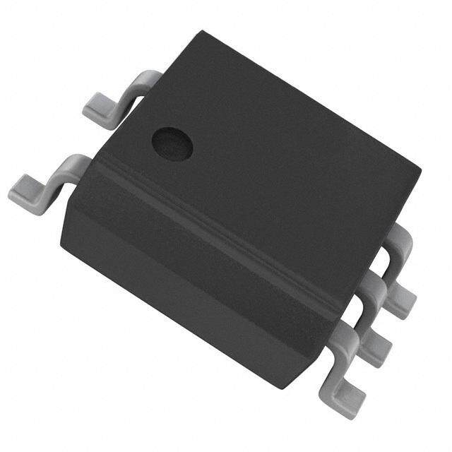
| 描述 | ISOLATOR 5KVRMS 1CH OPEN 8-SMD高速光耦合器 8 PW DIP HIGH SPEED LOGIC GATE OPTOCOUP |
| 产品分类 | |
| 品牌 | Fairchild Semiconductor |
| 产品手册 | |
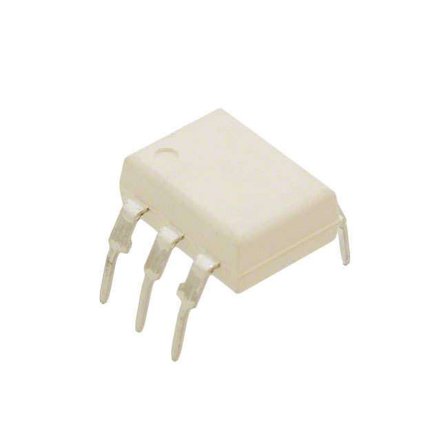
| 产品图片 |
|
| rohs | 符合RoHS无铅 / 符合限制有害物质指令(RoHS)规范要求 |
| 产品系列 | 光耦合器/光电耦合器,高速光耦合器,Fairchild Semiconductor 6N137SDM- |
| 数据手册 | |
| 产品型号 | 6N137SDM |
| 上升/下降时间(典型值) | 30ns, 10ns |
| 上升时间 | 75 ns |
| 下降时间 | 75 ns |
| 产品种类 | 高速光耦合器 |
| 传播延迟tpLH/tpHL(最大值) | 75ns, 75ns |
| 供应商器件封装 | 8-SMD |
| 共模瞬态抗扰度(最小值) | 10kV/µs(标准) |
| 其它名称 | 6N137SDMCT |
| 包装 | 剪切带 (CT) |
| 单位重量 | 720 mg |
| 商标 | Fairchild Semiconductor |
| 安装类型 | 表面贴装 |
| 封装 | Reel |
| 封装/外壳 | 8-SMD,鸥翼型 |
| 封装/箱体 | SMD-8 |
| 工作温度 | -40°C ~ 85°C |
| 工厂包装数量 | 1000 |
| 数据速率 | 10Mbps |
| 最大功率耗散 | 100 mW |
| 最大反向二极管电压 | 5 V |
| 最大工作温度 | + 100 C |
| 最大正向二极管电压 | 1.75 V |
| 最小工作温度 | - 40 C |
| 标准包装 | 1 |
| 正向电流 | 50 mA |
| 每芯片的通道数量 | 1 Channel |
| 电压-正向(Vf)(典型值) | 1.4V |
| 电压-电源 | 4.5 V ~ 5.5 V |
| 电压-隔离 | 5000Vrms |
| 电流-DC正向(If) | 50mA |
| 电流-输出/通道 | 50mA |
| 系列 | 6N137M |
| 绝缘电压 | 5000 Vrms |
| 输入-输入侧1/输入侧2 | 1/0 |
| 输入类型 | DC |
| 输出类型 | 开路集电极 |
| 输出设备 | Photo IC |
| 通道数 | 1 |


- 商务部:美国ITC正式对集成电路等产品启动337调查
- 曝三星4nm工艺存在良率问题 高通将骁龙8 Gen1或转产台积电
- 太阳诱电将投资9.5亿元在常州建新厂生产MLCC 预计2023年完工
- 英特尔发布欧洲新工厂建设计划 深化IDM 2.0 战略
- 台积电先进制程称霸业界 有大客户加持明年业绩稳了
- 达到5530亿美元!SIA预计今年全球半导体销售额将创下新高
- 英特尔拟将自动驾驶子公司Mobileye上市 估值或超500亿美元
- 三星加码芯片和SET,合并消费电子和移动部门,撤换高东真等 CEO
- 三星电子宣布重大人事变动 还合并消费电子和移动部门
- 海关总署:前11个月进口集成电路产品价值2.52万亿元 增长14.8%


PDF Datasheet 数据手册内容提取
Is Now Part of To learn more about ON Semiconductor, please visit our website at www.onsemi.com Please note: As part of the Fairchild Semiconductor integration, some of the Fairchild orderable part numbers will need to change in order to meet ON Semiconductor’s system requirements. Since the ON Semiconductor product management systems do not have the ability to manage part nomenclature that utilizes an underscore (_), the underscore (_) in the Fairchild part numbers will be changed to a dash (-). This document may contain device numbers with an underscore (_). Please check the ON Semiconductor website to verify the updated device numbers. The most current and up-to-date ordering information can be found at www.onsemi.com. Please email any questions regarding the system integration to Fairchild_questions@onsemi.com. ON Semiconductor and the ON Semiconductor logo are trademarks of Semiconductor Components Industries, LLC dba ON Semiconductor or its subsidiaries in the United States and/or other countries. ON Semiconductor owns the rights to a number of patents, trademarks, copyrights, trade secrets, and other intellectual property. A listing of ON Semiconductor’s product/patent coverage may be accessed at www.onsemi.com/site/pdf/Patent-Marking.pdf. ON Semiconductor reserves the right to make changes without further notice to any products herein. ON Semiconductor makes no warranty, representation or guarantee regarding the suitability of its products for any particular purpose, nor does ON Semiconductor assume any liability arising out of the application or use of any product or circuit, and specifically disclaims any and all liability, including without limitation special, consequential or incidental damages. Buyer is responsible for its products and applications using ON Semiconductor products, including compliance with all laws, regulations and safety requirements or standards, regardless of any support or applications information provided by ON Semiconductor. “Typical” parameters which may be provided in ON Semiconductor data sheets and/or specifications can and do vary in different applications and actual performance may vary over time. All operating parameters, including “Typicals” must be validated for each customer application by customer’s technical experts. ON Semiconductor does not convey any license under its patent rights nor the rights of others. ON Semiconductor products are not designed, intended, or authorized for use as a critical component in life support systems or any FDA Class 3 medical devices or medical devices with a same or similar classification in a foreign jurisdiction or any devices intended for implantation in the human body. Should Buyer purchase or use ON Semiconductor products for any such unintended or unauthorized application, Buyer shall indemnify and hold ON Semiconductor and its officers, employees, subsidiaries, affiliates, and distributors harmless against all claims, costs, damages, and expenses, and reasonable attorney fees arising out of, directly or indirectly, any claim of personal injury or death associated with such unintended or unauthorized use, even if such claim alleges that ON Semiconductor was negligent regarding the design or manufacture of the part. ON Semiconductor is an Equal Opportunity/Affirmative Action Employer. This literature is subject to all applicable copyright laws and is not for resale in any manner.
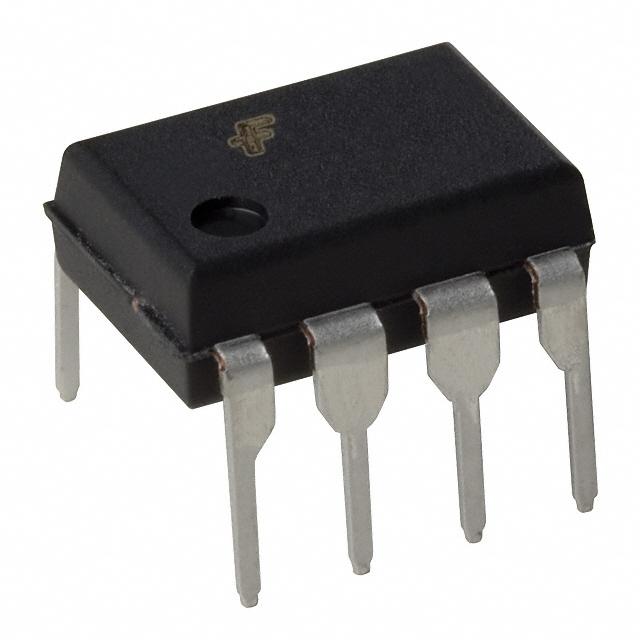
DS uin ag l -l January 2016 Ce h-C ah na nn en Single-Channel: 6N137M, HCPL2601M, HCPL2611M l :e Hl: Dual-Channel: HCPL2630M, HCPL2631M C 6 PN 8-Pin DIP High-Speed 10 MBit/s Logic Gate Optocouplers L1 23 67 3M 0, Features Description M H , C • Very High Speed – 10 MBit/s The 6N137M, HCPL2601M, HCPL2611M single-channel HP • Superior CMR – 10 kV/µs and HCPL2630M, HCPL2631M dual-channel optocou- CL P2 • Fan-out of 8 Over -40°C to +85°C plers consist of a 850 nm AlGaAS LED, optically coupled L6 to a very high speed integrated photo-detector logic gate 20 • Logic Gate Output 61 with a strobable output. This output features an open col- 3M • Strobable Output lector, thereby permitting wired OR outputs. The 1M, H • Wired OR-open Collector switching parameters are guaranteed over the tempera- —C • Safety and Regulatory Approvals ture range of -40°C to +85°C. A maximum input signal of P – UL1577, 5,000 VACRMS for 1 Minute 5 mA will provide a minimum output sink current of 8-PL2 – DIN EN/IEC60747-5-5 13mA (fan out of 8). in61 Applications An internal noise shield provides superior common mode D1M rejection of typically 10 kV/µs. The HCPL2601M and IP • Ground Loop Elimination HCPL2631M has a minimum CMR of 5 kV/µs. The H • LSTTL to TTL, LSTTL or 5 V CMOS HCPL2611M has a minimum CMR of 10 kV/µs. i g • Line Receiver, Data Transmission h - S • Data Multiplexing p • Switching Power Supplies e e • Pulse Transformer Replacement d 1 • Computer-peripheral Interface 0 M B Schematics Package Outlines i t / s L o 8 8 gi c N/C 1 8 VCC + 1 8 VCC 1 1 G a t V e F1 O + 2 7 VE _ 2 7 V01 p t V 8 o F 8 c _ 3 6 VO _ 3 6 V02 1 1 oup Figure 2. Package Options l V e F2 r Truth Table (Positive Logic) s N/C4 5 GND + 4 5 GND Input Enable Output H H L 6N137M, HCPL2630M, L H H HCPL2601M, HCPL2631M H L H HCPL2611M L L H A 0.1µF bypass capacitor must be connected between pins 8 and 5(1). H NC L Figure 1. Schematics L NC H ©2009 Fairchild Semiconductor Corporation www.fairchildsemi.com 6N137M, HCPL26XXM Rev. 1.6
DS uin Safety and Insulation Ratings ag l -l Ce As per DIN EN/IEC 60747-5-5, this optocoupler is suitable for “safe electrical insulation” only within the safety limit h-C data. Compliance with the safety ratings shall be ensured by means of protective circuits. ah n a Parameter Characteristics nn en l < 150 VRMS I–IV : Hel: Installation Classifications per DIN VDE < 300 VRMS I–IV C 6 PN 0110/1.89 Table 1, For Rated Mains Voltage < 450 VRMS I–III L1 23 < 600 V I–III 67 RMS 3M Climatic Classification 40/100/21 0, M H Pollution Degree (DIN VDE 0110/1.89) 2 , C H P Comparative Tracking Index 175 CL P2 L6 20 61 Symbol Parameter Value Unit 3M 1, Input-to-Output Test Voltage, Method A, V x 1.6 = V , M H Type and Sample Test with t = 10 s, PartIiOaRl DMischarge <P R5 pC 1,335 Vpeak —C m P V PR 8L I1n0p0u%t-t oP-rOoduutpcutito Tne Tset sVt owltiathg et, M =e 1th so, dP Bar, tViaIlO DRiMs cxh 1a.r8g7e5 < = 5 V pPCR, 1,669 Vpeak -P26 m in1 VIORM Maximum Working Insulation Voltage 890 Vpeak D1M V Highest Allowable Over-Voltage 6,000 V IP IOTM peak External Creepage ≥ 8.0 mm H i g External Clearance ≥ 7.4 mm h - External Clearance (for Option TV, 0.4" Lead Spacing) ≥ 10.16 mm S p DTI Distance Through Insulation (Insulation Thickness) ≥ 0.5 mm e e TS Case Temperature(2) 150 °C d 1 I Input Current(2) 200 mA 0 S,INPUT M PS,OUTPUT Output Power (Duty Factor ≤ 2.7%)(2) 300 mW B R Insulation Resistance at T , V = 500 V(2) > 109 Ω it IO S IO / s Notes: L o 1. The V supply to each optoisolator must be bypassed by a 0.1 µF capacitor or larger. This can be either a ceramic g CC or solid tantalum capacitor with good high frequency characteristic and should be connected as close as possible to ic the package VCC and GND pins of each device. G 2. Safety limit value - maximum values allowed in the event of a failure. a t e O p t o c o u p l e r s ©2009 Fairchild Semiconductor Corporation www.fairchildsemi.com 6N137M, HCPL26XXM Rev. 1.6 2
DS uin Absolute Maximum Ratings ag l -l Stresses exceeding the absolute maximum ratings may damage the device. The device may not function or be Ce operable above the recommended operating conditions and stressing the parts to these levels is not recommended. h-C ah In addition, extended exposure to stresses above the recommended operating conditions may affect device reliability. n a The absolute maximum ratings are stress ratings only. T = 25°C unless otherwise specified. nn A en l :e Symbol Parameter Value Unit Hl: T Storage Temperature -40 to +125 °C C 6 STG PN T Operating Temperature -40 to +100 °C L1 OPR 23 TJ Junction Temperature -40 to +125 °C 637M TSOL Lead Solder Temperature 260 for 10 sec °C 0M, H Symbol Parameter Device Value Unit , C H P EMITTER CL P2 Single Channel 50 L6 I (avg) DC/Average Forward Input Current Per Channel mA 20 F 61 Dual Channel 30 3M V Enable Input Voltage Not to Exceed VCC Single Channel 5.5 V 1M, H E by more than 500 mV —C P V Reverse Input Voltage Per Channel All 5.0 V R 8L Single Channel 100 -P26 PI Input Power Dissipation Per Channel mW in1 Dual Channel 45 1 DM DETECTOR IP V Supply Voltage All -0.5 to 7.0 V H CC i g I (avg) Average Output Current Per Channel All 25 mA O h - I (pk) Peak Output Current Per Channel All 50 mA S O p V Output Voltage Per Channel All -0.5 to 7.0 V e O e Single Channel 85 d PO Output Power Dissipation Per Channel mW 1 Dual Channel 60 0 M B i t / s Recommended Operating Conditions L o The Recommended Operating Conditions table defines the conditions for actual device operation. Recommended g operating conditions are specified to ensure optimal performance to the datasheet specifications. Fairchild does not ic recommend exceeding them or designing to absolute maximum ratings. G a Symbol Parameter Min. Max. Unit t e V Supply Voltage 4.5 5.5 V O CC p IFL Input Current, Low Level 0 250 µA to IFH Input Current, High Level 6.3(3) 20.0 mA co u VEL Enable Voltage, Low Level 0 0.8 V p l V Enable Voltage, High Level 2.0 V V e EH CC r s T Ambient Operating Temperature -40 +85 °C A N Fan Out (TTL load) 8 Note: 3. 6.3 mA is a guard banded value which allows for at least 20% CTR degradation. Initial input current threshold value is 5.0 mA or less. ©2009 Fairchild Semiconductor Corporation www.fairchildsemi.com 6N137M, HCPL26XXM Rev. 1.6 3
DS uin Electrical Characteristics ag l -l Ce Individual Component Characteristics (VCC = 5.5 V, TA = 0°C to 70°C unless otherwise specified) h-C ah Symbol Parameter Device Test Conditions Min. Typ. Max. Unit na nn EMITTER eln :e VF Input Forward Voltage All IF = 10 mA, TA = 25°C 1.45 1.70 V HCl: 6 IF = 10 mA 1.80 PN L1 B Input Reverse Breakdown All I = 10 µA 5.0 V 23 VR Voltage R 67 3M CIN Input Capacitance All VF = 0, f = 1 MHz 60 pF 0M, H ΔV / ΔT Temperature Coefficient of All I = 10 mA -1.4 mV/°C , HC F A Forward Voltage F P CL DETECTOR P2 L6 I = 10 mA, V = Open, 20 Single Channel F O 8 13 61 VE = 0.5 V 3M ICCL Logic Low Supply Current Dual Channel IF1 = IF2 = 10 mA, 14 21 mA 1M, H VO = Open —C P ICCH Logic High Supply Current Single Channel VIFE = = 0 0 m.5A V, VO = Open, 6 10 mA 8-P L26 Dual Channel I = 0 mA, V = Open, 10 15 in1 F O 1 DM IEL Low Level Enable Current Single Channel VE = 0.5 V -0.7 -1.6 mA IP IEH High Level Enable Current Single Channel VE = 2.0 V -0.5 -1.6 mA H V Low Level Enable Voltage Single Channel I = 10 mA(4) 0.8 V ig EL F h V High Level Enable Voltage Single Channel I = 10 mA 2.0 V - EH F S p Note: e e 4. Enable Input – No pull up resistor required as the device has an internal pull up resistor. d 1 0 M Transfer Characteristics (V = 5.5 V, T = -40°C to +85°C unless otherwise specified) B CC A i t Symbol Parameter Device Test Conditions Min. Typ. Max. Unit / s V = 0.6 V, V = 2.0 V, L I Input Threshold Current All O E 3 5 mA o FT IOL = 13 mA g i V = 5.5 V, I = 250 µA, c IOH HIGH Level Output Current All VO = 2.0 V F 100 µA G E a VOL LOW Level Output Voltage All IIF = =5 1m3A m, AVE = 2.0 V, 0.4 0.6 V te O OL p t o c o u p l e r s ©2009 Fairchild Semiconductor Corporation www.fairchildsemi.com 6N137M, HCPL26XXM Rev. 1.6 4
DS uin Electrical Characteristics (Continued) ag l -l Ce Switching Characteristics (VCC = 5 V, IF = 7.5 mA, TA = -40°C to +85°C unless otherwise specified) h-C ah Symbol Parameter Device Test Conditions Min. Typ. Max. Unit n a tPHL PTirmopea tgoa Ltioogni cD LeOlaWy All RTR(FALLi g===. 21335455°)00C ΩΩ(5,,) CC(FLLi g==. 111554 )ppFF,(5) 25 40 17050 ns nel: HCPnnel: 6N L1 R = 350 Ω, C = 15 pF, 23 Propagation Delay TAL = 25°C(6) (FLig. 14) 20 40 75 637M tPLH Time to Logic HIGH All RL = 350 Ω, CL = 15 pF(6) 100 ns 0M, H (Fig. 14) , C H P |t –t | Pulse Width Distortion All RL = 350 Ω, CL = 15 pF 1 35 ns CL PHL PLH (Fig. 14) P2 L6 Output Rise Time R = 350 Ω, C = 15 pF(7) 20 t All L L 30 ns 61 R (10% to 90%) (Fig. 14) 3M t Output Fall Time All RL = 350 Ω, CL = 15 pF(8) 10 ns 1M, H F (90% to 10%) (Fig. 14) —C P tEHL EDnealabyl eT Pimroep taog Oatuiotpnu t Single Channel CVE H= =1 53 .p5F V(9, )R (LF i=g .3 1550) Ω, 15 ns 8-P L26 LOW Level L in1 1 Enable Propagation DM t Delay Time to Output Single Channel VEH = 3.5 V, RL = 350 Ω, 15 ns IP ELH HIGH Level CL = 15 pF(10) (Fig. 15) H i g 6N137M, I = 0 mA, V = 50 V , 10,000 h HCPL2630M F CM PEAK - R = 350 Ω, T = 25°C(11) S Common Mode HCPL2601M, L A p (Fig. 16) 5000 10,000 e |CM | Transient Immunity HCPL2631M V/µs e H d at Logic High I = 0 mA, V = 400 V , F CM PEAK 1 HCPL2611M R = 350 Ω, T = 25°C(11) 10,000 15,000 0 L A (Fig. 16) M B 6N137M, i HCPL2630M VCM = 50 VPEAK, 10,000 t/s Common Mode HCPL2601M, RL = 350 Ω, TA = 25°C(11) L (Fig. 16) 5000 10,000 o |CML| Transient Immunity HCPL2631M V/µs g at Logic Low ic V = 400 V , CM PEAK HCPL2611M R = 350 Ω, T = 25°C(11) 10,000 15,000 G L A a (Fig. 16) t e O Notes: p 5. t – Propagation delay is measured from the 3.75 mA level on the LOW to HIGH transition of the input current t PHL o pulse to the 1.5 V level on the HIGH to LOW transition of the output voltage pulse. c 6. t – Propagation delay is measured from the 3.75 mA level on the HIGH to LOW transition of the input current o PLH u pulse to the 1.5 V level on the LOW to HIGH transition of the output voltage pulse. p 7. t – Rise time is measured from the 90% to the 10% levels on the LOW to HIGH transition of the output pulse. le R r 8. t – Fall time is measured from the 10% to the 90% levels on the HIGH to LOW transition of the output pulse. s F 9. t – Enable input propagation delay is measured from the 1.5 V level on the LOW to HIGH transition of the input EHL voltage pulse to the 1.5 V level on the HIGH to LOW transition of the output voltage pulse. 10.t – Enable input propagation delay is measured from the 1.5 V level on the HIGH to LOW transition of the input ELH voltage pulse to the 1.5 V level on the LOW to HIGH transition of the output voltage pulse. 11.Common mode transient immunity in logic high level is the maximum tolerable (positive) dV /dt on the leading edge cm of the common mode pulse signal, V , to assure that the output will remain in a logic high state (i.e., V > 2.0 V). CM O Common mode transient immunity in logic low level is the maximum tolerable (negative) dV /dt on the trailing edge cm of the common mode pulse signal, V , to assure that the output will remain in a logic low state (i.e., V < 0.8 V). CM O ©2009 Fairchild Semiconductor Corporation www.fairchildsemi.com 6N137M, HCPL26XXM Rev. 1.6 5
DS uin Electrical Characteristics (Continued) ag l -l Ce Isolation Characteristics (TA =25°C unless otherwise specified.) h-C ah Symbol Parameter Device Test Conditions Min. Typ. Max. Unit n a nn Relative Humidity ≤ 50%, en Withstand Insulation l VISO Test Voltage All IfI -=O 5≤0 1 H0z µ(1A2,) (t1 3=) 1 min, 5,000 VACRMS : HCel: 6 Resistance PN R All V = 500 V (12) 1011 Ω L1 I-O (Input to Output) I-O DC 23 67 Capacitance 3M CI-O (Input to Output) All f = 1 MHz, VI-O = 0 VDC(12) 1 pF 0M, H Input-Output Insulation Relative Humidity ≤ 45%, , C II-O Leakage Current All VI-I = 3000 VDC, t = 5 sec(12) 1.0 µA HCPL P2 Notes: L6 20 12.Device is considered a two terminal device: pins 1, 2, 3 and 4 are shorted together and pins 5, 6, 7 and 8 are shorted 61 together. 3M 1, 13. 5000 VACRMS for 1 minute duration is equivalent to 6000 VACRMS for 1 second duration. M H —C P 8L -P2 6 in1 1 DM IP H i g h - S p e e d 1 0 M B i t / s L o g i c G a t e O p t o c o u p l e r s ©2009 Fairchild Semiconductor Corporation www.fairchildsemi.com 6N137M, HCPL26XXM Rev. 1.6 6
DS uin Typical Performance Curves ag l -l Ce For Single-Channel Devices: 6N137M, HCPL2601M, and HCPL2611M h-C ah n a 0.8 nn en )V( EGATLO 00..76 IVVFEC = C= 5 =2 m 5V.A5 V IOL = 12.8 mA )Am( TN 10 l: HCPel: 6N V TUP 0.5 IOL = 16 mA ERRU 1 L26137 TUO LEVEL WOL – 000...432 IOL = 9.6 mA IOL = 6.4 mA C DRAWROF – IF 00..011000 30M, HCPM, HCPL2 LO 0.1 L6 V 20 0.0 0.001 61 -40 -20 0 20 40 60 80 100 0.9 1.0 1.1 1.2 1.3 1.4 1.5 1.6 3M TA – AMBIENT TEMPERATURE (°C) VF – FORWARD VOLTAGE (V) 1M, H Figure 3. Low Level Output Voltage vs. Ambient Temperature Figure 4. Input Diode Forward Voltage vs. Forward Current —C P 8L 120 50 -P26 VCC = 5 V in1 )sn( Y 100 TA = 25°C )Am( TNER 45 IF = 15 mA DIP H1M ALED NOIT 6800 RL = 4 kΩ (tPLH) RL = 350 Ω (tPLH) RUC TUPT 3450 IF = 10 mA igh-S AG RL = 1 kΩ (tPLH) UO p AP LE IF = 5 mA e O 40 V 30 e RP – TP 20 RRRLLL === 413 5kk0ΩΩ Ω ((tt PP(tHHPLLH))L) EL WOL – LO 25 VVVCEO CL= = =2 0 5V. 6V V d 10 M 0 I 20 B 5 7 9 11 13 15 -40 -20 0 20 40 60 80 100 it IF – FORWARD CURRENT (mA) TA – AMBIENT TEMPERATURE (°C) /s Figure 5. Switching Time vs. Forward Current Figure 6. Low Level Output vs. Ambient Temperature L o g i c 4.0 6 G a )Am 3.5 VVCE C= =2 5V V 5 te ( T VOL = 0.6 V O NERRUC DLOHSERHT TUPNI – 3221....0505 RRRLLL === 3145 kk0ΩΩ Ω )V( EGATLOV TUPTUO – VO 1234 RL = 4 kΩ RL =R 3L5 =0 1Ω kΩ ptocouplers ITF 1.0 0 -40 -20 0 20 40 60 80 100 0 1 2 3 4 5 6 TA – AMBIENT TEMPERATURE (°C) IF - FORWARD CURRENT (mA) Figure 7. Input Threshold Current vs. Ambient Temperature Figure 8. Output Voltage vs. Input Forward Current ©2009 Fairchild Semiconductor Corporation www.fairchildsemi.com 6N137M, HCPL26XXM Rev. 1.6 7
DS uin Typical Performance Curves (Continued) ag l -l Ce For Single-Channel Devices: 6N137M, HCPL2601M, HCPL2611M h-C ah n a 60 500 nn en )sn( NOITR 5400 VIFC =C 7=. 55 mVA )sn( EM 400 IVFC =C 7=. 55 mVA RL = 4 kΩ (tR) l: HCPel: 6N OTSID HTDIW 3200 RL = 4 kΩ IT LLAF DNA E 320000 L2630M137M, H ESLUP – DWP 100 RRLL = = 1 3 k5Ω0 Ω SIR – t / tFR 1000 RRRRLLLL ==== 1341 5 kkk0ΩΩΩ Ω (((ttt RFF(t)))R) , HCPL2CPL260 -10-40 -20 0 20 40 60 80 100 -100-40 -20 0 2R0L = 350 Ω4 (0tF) 60 80 100 631M TA – AMBIENT TEMPERATURE (°C) TA – AMBIENT TEMPERATURE (°C) 1M, H Figure 9. Pulse Width Distortion vs. Temperature Figure 10. Rise and Fall Time vs. Temperature —C P 8L )s 100 100 -P26 n( YALE VIFC =C 7=. 55 mVA 90 IVFC =C 7=. 55 mVA in D11M D NOITAGA 8600 RL = 4 kΩ (tELH) )sn( YALE 8700 RL = 4 kΩ (tPLH) IP Hig P D h ORP ELBANE – TE 4200 RRL L= =1 4k ΩkΩ (t E/ L1H k)Ω / R35L 0= Ω 3 5(t0E HΩL )(tELH) NOITAGAPORP – TP 65430000 RL = 350 ΩR (LtP =L H1) kΩ (tPLH) RRRLLL === 413 5kk0ΩΩ Ω ((tt PP(tHHPLLH))L) -Speed 10 M B 0 20 -40 -20 0 20 40 60 80 100 -40 -20 0 20 40 60 80 100 it TA – AMBIENT TEMPERATURE (°C) TA – AMBIENT TEMPERATURE (°C) /s L Figure 11. Enable Propagation Delay vs. Temperature Figure 12. Switching Time vs. Temperature o g i c 1.6 G μ)A 1.4 VCC = 5 V at ( T VO = 5.5 V e NER 1.2 VIFE = = 2 25 0V μA O R p UC TU 1.0 toc PTU 0.8 ou O L p EV 0.6 le EL r HG 0.4 s IH – H 0.2 O I 0 -40 -20 0 20 40 60 80 100 TA – AMBIENT TEMPERATURE (°C) Figure 13. High Level Output Current vs. Temperature ©2009 Fairchild Semiconductor Corporation www.fairchildsemi.com 6N137M, HCPL26XXM Rev. 1.6 8
DS uin Typical Performance Curves (Continued) ag l -l Ce For Dual-Channel Devices: HCPL2630M and HCPL2631M h-C ah n a )V( EGATLOV TUPTUO LEVEL WOL 0000000.......2345678 IVF C=C 5= m5.A5 V IOL I=O L1 =2 .68. 4m mAA IOL I=O L1 =6 9m.6A mA )Am( TNERRUC DRAWROF – 01.0100.01011 nel: HCPL2630M, Hnnel: 6N137M, HCP – VLO 0.1 IF CPL2 0.0 0.001 L6 -40 -20 0 20 40 60 80 100 0.9 1.0 1.1 1.2 1.3 1.4 1.5 1.6 20 61 TA – AMBIENT TEMPERATURE (°C) VF – FORWARD VOLTAGE (V) 3M Figure 14. Low Level Output Voltage vs. Ambient Temperature Figure 15. Input Diode Forward Voltage 1M, H vs. Forward Current —C P 120 50 8L )sn( YALED N 18000 VTAC C= = 2 55 °V C RL = 4 kΩ (TPLH) )Am( TNERRUC 4405 IIFF == 1105 mmAA -Pin DIP2611M OIT TU IF = 5 mA H AGAP 60 RL = 1 kΩ (TPLH) PTUO 35 igh ORP 40 RL = 350 Ω (TPLH) LEV 30 -S – TP 20 RRRLLL === 143 5kk0ΩΩ Ω(T PHL) EL WOL – 25 VVCOCL == 05. 6V V peed 05 7 9 11 13 15 ILO 20-40 -20 0 20 40 60 80 100 10 IF – FORWARD CURRENT (mA) TA – AMBIENT TEMPERATURE (°C) M B Figure 16. Switching Time vs. Forward Current Figure 17.Low Level Output Current i vs. Ambient Temperature t / s )Am 4 6 Lo ( TNERRUC DLOHS 3 VVCOCL == 50..06 VV RRLL = = 13 5kΩ0 Ω )V( EGATLOV T 345 RL = 4 k Ω RL = 350 Ω gic Gate O ER RL = 4 kΩ UP p HT T 2 TUO 2 to UPNI – – VO 1 RL = 1 kΩ cou ITF pl e 1 0 r -40 -20 0 20 40 60 80 100 0 1 2 3 4 5 6 s TA – AMBIENT TEMPERATURE (°C) IF - FORWARD CURRENT (mA) Figure 18. Input Threshold Current Figure 19. Output Voltage vs. Input Forward Current vs. Ambient Temperature ©2009 Fairchild Semiconductor Corporation www.fairchildsemi.com 6N137M, HCPL26XXM Rev. 1.6 9
DS uin Typical Performance Curves (Continued) ag l -l Ce For Dual-Channel Devices: HCPL2630M and HCPL2631M h-C ah n a 80 600 nn )s eln n :e ( NOIT 60 RL = 4 kΩ )sn( E 500 VIFC =C 7=. 55 mVA HCl: 6 ROTSID HT 40 IVFC =C 7=. 55 mVA MIT LLAF D 430000 RL = 4 kΩ(tr) PL263N137M DIW ESLUP – DWP 20 RL = 1 kΩ RL = 350 Ω NA ESIR – fT/rT 210000 RL = 35R0 LΩ = ( t1r )kΩ(tr) RRRLLL === 143 5kk0ΩΩ Ω( tf) 0M, HCPL, HCPL26 0 0 20 -60 -40 -20 0 20 40 60 80 100 -60 -40 -20 0 20 40 60 80 100 61 3M TA – TEMPERATURE (°C) TA – TEMPERATURE (°C) 1, M H Figure 20. Pulse Width Distortion vs. Temperature Figure 21.Rise and Fall Time vs. Temperature —C P 8L 120 )A 1.8 -P26 )sn( YALED NO 18000 RL = 4 kΩ (TPLH) IVFC =C 7=. 55 mVA μ( TNERRUC TUPT 1111....6420 VVIFCO =C = 2= 55 5.05. 5 μV AV in DIP Hig11M IT U h AGAPOR 60 RL = 1 kΩ (TPLH) O LEVEL 00..86 -Spe P – 40 RL = 350 Ω (TPLH) HG 0.4 ed TP RRLL == 14 kkΩΩ (TPHL) IH – H 0.2 10 20 RL = 350 Ω IO 0 M -60 -40 -20 0 20 40 60 80 100 -60 -40 -20 0 20 40 60 80 100 B TA – TEMPERATURE (°C) TA – TEMPERATURE (°C) i t Figure 23. High Level Output Current / s Figure 22. Switching Time vs. Temperature vs. Temperature L o g i c G a t e O p t o c o u p l e r s ©2009 Fairchild Semiconductor Corporation www.fairchildsemi.com 6N137M, HCPL26XXM Rev. 1.6 10
DS uin Test Circuits ag l -l Ce h-C ah Pulse na Generator nn tr = 5 ns en Z O = 50 Ω +5V l: Hel: C 6 I = 7.5 mA PN F V L1 1 CC 8 I(nI p )ut I F = 3.75 mA 2637 F 3M tPHL tPLH 0, 2 7 .1 μF R Output M H bypass L (VO ) 1.5 V , HCP Output CL IMnopnuittor 3 6 (VO ) Output 90% PL26 (I F ) CL (V ) 20 O 10% 61 47 4 5 3M GND tf tr 1M, H —C P 8L -P2 6 Figure 24. Test Circuit and Waveforms for tPLH, tPHL, trand tf in1 1 DM IP H Pulse i Generator Input g tr = 5 ns Monitor h Z O = 50 Ω (V E ) -S p +5V e e d 3.0 V 1 V Input 0 1 CC 8 (VE ) 1.5 V M B t t 7.5 mA EHL ELH i 2 7 .1 μF RL (OVuO t)put t/s bypass 1.5 V L Output o 3 6 g (VO ) i C c L G 4 5 a GND t e O p t o Figure 25. Test Circuit tEHLand tELH c o u p l e r s ©2009 Fairchild Semiconductor Corporation www.fairchildsemi.com 6N137M, HCPL26XXM Rev. 1.6 11
DS uin Test Circuits (Continued) ag l -l Ce h-C ah n a V nn CC en 1 8 +5 V l :e Hl: C 6 A IF 2 7 .1 μF 350 Ω PLN1 bypass 23 B 67 3M Output VFF 3 6 (VO ) 0M, H , C H P 4 5 CL GND P2 L6 20 61 3M V CM 1, M H Pulse Gen —C P 8L -P2 6 Peak in1 1 DM IP VCM 0V H i g h - S 5V CMH p Switching Pos. (A), IF = 0 e VO e d VO (Min) 1 0 M V (Max) B O i t / Switching Pos. (B), I = 7.5 mA s VO F L 0.5 V CML o g i c G a t e Figure 26. Test Circuit Common Mode Transient Immunity O p t o c o u p l e r s ©2009 Fairchild Semiconductor Corporation www.fairchildsemi.com 6N137M, HCPL26XXM Rev. 1.6 12
DS uin Reflow Profile ag l -l Ce h-C ah n a TP MMaxaixmimumum R Ramamp-pd-ouwp nR Rataet e= =3 °6C°C/S/S nelnn 260 :e 240 tP HCl: 6 220 TL PN L1 200 Tsmax 23 ) 180 Preheat Area tL 637M C 0, e (° 116400 Tsmin M, HC ur ts HP t 120 CL era 100 PL26 p 20 m 80 61 Te 60 31M, 40 M H —C 20 P 0 8L -P2 120 240 360 6 in1 Time 25°C to Peak D1M Time (seconds) IP H i g h - S p e Profile Freature Pb-Free Assembly Profile e d Temperature Min. (Tsmin) 150°C 1 0 Temperature Max. (Tsmax) 200°C M Time (tS) from (Tsmin to Tsmax) 60 to 120 s B i Ramp-up Rate (tL to tP) 3°C/second maximum t/s Liquidous Temperature (T ) 217°C L L o Time (t ) Maintained Above (T ) 60 to 150 s g L L i c Peak Body Package Temperature 260°C +0°C / –5°C G Time (t ) within 5°C of 260°C 30 s a P t e Ramp-down Rate (TP to TL) 6°C/s maximum O Time 25°C to Peak Temperature 8 minutes maximum p t o c Figure 27. Reflow Profile o u p l e r s ©2009 Fairchild Semiconductor Corporation www.fairchildsemi.com 6N137M, HCPL26XXM Rev. 1.6 13
DS uin Ordering Information ag l -l Ce Part Number Package Packing Method h-C ah 6N137M DIP 8-Pin Tube (50 units per tube) n a nn 6N137SM SMT 8-Pin (Lead Bend) Tube (50 units per tube) en l :e 6N137SDM SMT 8-Pin (Lead Bend) Tape and Reel (1,000 units per reel) Hl: 6N137VM DIP 8-Pin, DIN EN/IEC 60747-5-5 Option Tube (50 units per tube) C 6 PN 6N137SVM SMT 8-Pin (Lead Bend), DIN EN/IEC 60747-5-5 Option Tube (50 units per tube) L1 23 6N137SDVM SMT 8-Pin (Lead Bend), DIN EN/IEC 60747-5-5 Option Tape and Reel (1,000 units per reel) 67 3M 6N137TVM DIP 8-Pin, 0.4” Lead Spacing, DIN EN/IEC 60747-5-5 Option Tube (50 units per tube) 0, M H 6N137TSVM SMT 8-Pin, 0.4” Lead Spacing, DIN EN/IEC 60747-5-5 Option Tube (50 units per tube) , C H P 6N137TSR2VM SMT 8-Pin, 0.4” Lead Spacing, DIN EN/IEC 60747-5-5 Option Tape and Reel (1,000 units per reel) CL P2 Note: L6 20 The product orderable part number system listed in this table also applies to the HCPL2601M, HCPL2611M, 61 3M HCPL2630M and HCPL2631M product families. 1, M H —C P 8L Marking Information -P2 6 in1 1 DM IP H 1 ig h - S 6N137 2 p e e V XX YY B 6 d 1 0 M B 3 4 5 i t / s Figure 28. Top Mark L o g i Definitions c G 1 Fairchild Logo a t e 2 Device Number O DIN EN/IEC60747-5-5 Option (only appears on component p 3 t ordered with this option) o c 4 Two Digit Year Code, e.g., ‘16’ o u 5 Two Digit Work Week Ranging from ‘01’ to ‘53’ p l e 6 Assembly Package Code r s ©2009 Fairchild Semiconductor Corporation www.fairchildsemi.com 6N137M, HCPL26XXM Rev. 1.6 14
DS uin Carrier Tape Specifications (Option SD) ag l -l Ce D h-C 0 ah t P0 P2 E nnan K0 en l :e Hl: C 6 PN F L1 A0 23 W1 B0 W 637M 0, M H , C H P CL P P2 d UserDirectionofFeed D L6 1 20 61 3M 1, Symbol Description Dimension in mm M H —C W Tape Width 16.0 ± 0.3 P 8L t Tape Thickness 0.30 ± 0.05 -P2 6 P Sprocket Hole Pitch 4.0 ± 0.1 in1 0 1 DM D0 Sprocket Hole Diameter 1.55 ± 0.05 IP E Sprocket Hole Location 1.75 ± 0.10 H i F Pocket Location 7.5 ± 0.1 g h P2 2.0 ± 0.1 -S p P Pocket Pitch 12.0 ± 0.1 e e A0 Pocket Dimensions 10.30 ±0.20 d 1 B 10.30 ±0.20 0 0 K 4.90 ±0.20 M 0 B W1 Cover Tape Width 13.2 ± 0.2 it / d Cover Tape Thickness 0.1 Maximum s L Maximum Component Rotation or Tilt 10° o g R Minimum Bending Radius 30 i c G a t e O p t o c o u p l e r s ©2009 Fairchild Semiconductor Corporation www.fairchildsemi.com 6N137M, HCPL26XXM Rev. 1.6 15
DS uin Carrier Tape Specifications (Option TSR2) ag l -l Ce D h-C 0 ah t P0 P2 E nnan K0 en l :e Hl: C 6 PN F L1 A0 23 W1 B0 W 637M 0, M H , C H P CL P P2 d UserDirectionofFeed D L6 1 20 61 3M 1, Symbol Description Dimension in mm M H —C W Tape Width 24.0 ± 0.3 P 8L t Tape Thickness 0.40 ± 0.1 -P2 6 P Sprocket Hole Pitch 4.0 ± 0.1 in1 0 1 DM D0 Sprocket Hole Diameter 1.55 ± 0.05 IP E Sprocket Hole Location 1.75 ± 0.10 H i F Pocket Location 11.5 ± 0.1 g h P2 2.0 ± 0.1 -S p P Pocket Pitch 16.0 ± 0.1 e e A0 Pocket Dimensions 12.80 ± 0.1 d 1 B 10.35 ± 0.1 0 0 K 5.7 ±0.1 M 0 B W1 Cover Tape Width 21.0 ± 0.1 it / d Cover Tape Thickness 0.1 Maximum s L Maximum Component Rotation or Tilt 10° o g R Minimum Bending Radius 30 i c G a t e O p t o c o u p l e r s ©2009 Fairchild Semiconductor Corporation www.fairchildsemi.com 6N137M, HCPL26XXM Rev. 1.6 16
None
None
None
None
ON Semiconductor and are trademarks of Semiconductor Components Industries, LLC dba ON Semiconductor or its subsidiaries in the United States and/or other countries. ON Semiconductor owns the rights to a number of patents, trademarks, copyrights, trade secrets, and other intellectual property. A listing of ON Semiconductor’s product/patent coverage may be accessed at www.onsemi.com/site/pdf/Patent−Marking.pdf. ON Semiconductor reserves the right to make changes without further notice to any products herein. ON Semiconductor makes no warranty, representation or guarantee regarding the suitability of its products for any particular purpose, nor does ON Semiconductor assume any liability arising out of the application or use of any product or circuit, and specifically disclaims any and all liability, including without limitation special, consequential or incidental damages. Buyer is responsible for its products and applications using ON Semiconductor products, including compliance with all laws, regulations and safety requirements or standards, regardless of any support or applications information provided by ON Semiconductor. “Typical” parameters which may be provided in ON Semiconductor data sheets and/or specifications can and do vary in different applications and actual performance may vary over time. All operating parameters, including “Typicals” must be validated for each customer application by customer’s technical experts. ON Semiconductor does not convey any license under its patent rights nor the rights of others. ON Semiconductor products are not designed, intended, or authorized for use as a critical component in life support systems or any FDA Class 3 medical devices or medical devices with a same or similar classification in a foreign jurisdiction or any devices intended for implantation in the human body. Should Buyer purchase or use ON Semiconductor products for any such unintended or unauthorized application, Buyer shall indemnify and hold ON Semiconductor and its officers, employees, subsidiaries, affiliates, and distributors harmless against all claims, costs, damages, and expenses, and reasonable attorney fees arising out of, directly or indirectly, any claim of personal injury or death associated with such unintended or unauthorized use, even if such claim alleges that ON Semiconductor was negligent regarding the design or manufacture of the part. ON Semiconductor is an Equal Opportunity/Affirmative Action Employer. This literature is subject to all applicable copyright laws and is not for resale in any manner. PUBLICATION ORDERING INFORMATION LITERATURE FULFILLMENT: N. American Technical Support: 800−282−9855 Toll Free ON Semiconductor Website: www.onsemi.com Literature Distribution Center for ON Semiconductor USA/Canada 19521 E. 32nd Pkwy, Aurora, Colorado 80011 USA Europe, Middle East and Africa Technical Support: Order Literature: http://www.onsemi.com/orderlit Phone: 303−675−2175 or 800−344−3860 Toll Free USA/Canada Phone: 421 33 790 2910 Fax: 303−675−2176 or 800−344−3867 Toll Free USA/Canada Japan Customer Focus Center For additional information, please contact your local Email: orderlit@onsemi.com Phone: 81−3−5817−1050 Sales Representative © Semiconductor Components Industries, LLC www.onsemi.com www.onsemi.com 1
Mouser Electronics Authorized Distributor Click to View Pricing, Inventory, Delivery & Lifecycle Information: O N Semiconductor: 6N137SDM 6N137SM 6N137SVM 6N137SDVM 6N137TSR2VM 6N137TSVM 6N137M 6N137VM 6N137TVM