ICGOO在线商城 > 隔离器 > 光隔离器 - 逻辑输出 > H11L1SM
/H11L1SM.jpg)
 Datasheet下载
- 型号: H11L1SM
- 制造商: Fairchild Semiconductor
- 库位|库存: xxxx|xxxx
- 要求:
| 数量阶梯 | 香港交货 | 国内含税 |
| +xxxx | $xxxx | ¥xxxx |
查看当月历史价格
查看今年历史价格
H11L1SM产品简介:
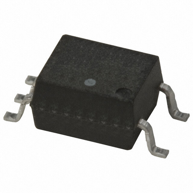
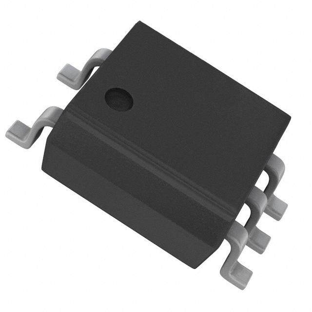
ICGOO电子元器件商城为您提供H11L1SM由Fairchild Semiconductor设计生产,在icgoo商城现货销售,并且可以通过原厂、代理商等渠道进行代购。 H11L1SM价格参考¥3.23-¥3.23。Fairchild SemiconductorH11L1SM封装/规格:光隔离器 - 逻辑输出, Logic Output Optoisolator 1MHz Open Collector 5000Vrms 1 Channel 6-SMD。您可以下载H11L1SM参考资料、Datasheet数据手册功能说明书,资料中有H11L1SM 详细功能的应用电路图电压和使用方法及教程。
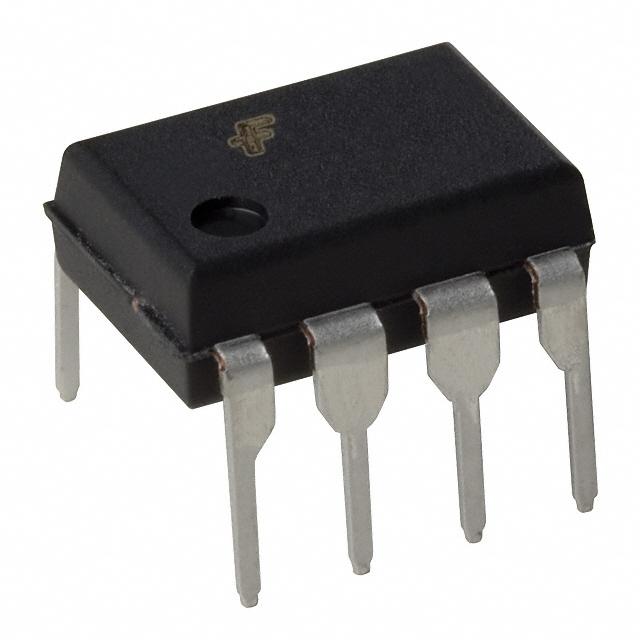
H11L1SM是Isocom Components 2004 LTD生产的一款光隔离器(光电耦合器),属于逻辑输出型光耦。该器件内部由一个红外发光二极管和一个集成有施密特触发器的光敏探测器组成,具有输入与输出之间电气隔离、抗干扰能力强、响应速度快等特点。

H11L1SM广泛应用于需要信号隔离的电子系统中,典型应用场景包括:工业自动化控制系统中的数字信号隔离,用于隔离微控制器与高电压或高噪声电路,防止干扰和损坏;开关电源反馈回路中实现控制侧与功率侧的隔离通信;PLC(可编程逻辑控制器)、仪器仪表和数据采集系统中的电平转换与噪声抑制;以及通信设备中对传输信号进行隔离保护。

此外,由于其具备施密特触发整形功能,能够有效消除输入信号抖动,提升信号稳定性,因此也适用于处理来自机械开关或传感器等不纯净信号的场合。H11L1SM采用小型DIP-6封装,便于在紧凑电路板上安装,适合要求高可靠性与安全隔离的中低速数字系统。
| 参数 | 数值 |
| 产品目录 | |
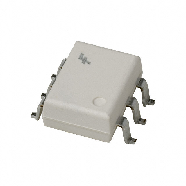
| 描述 | OPTOCOUPLER LOGIC OUT 6-SMD逻辑输出光电耦合器 SO-6 SCHMITT TRIG |
| 产品分类 | |
| 品牌 | Fairchild Semiconductor |
| 产品手册 | |
| 产品图片 |
|
| rohs | 符合RoHS无铅 / 符合限制有害物质指令(RoHS)规范要求 |
| 产品系列 | 光耦合器/光电耦合器,逻辑输出光电耦合器,Fairchild Semiconductor H11L1SM- |
| 数据手册 | |
| 产品型号 | H11L1SM |
| PCN设计/规格 | |
| 上升/下降时间(典型值) | 100ns, 100ns |
| 上升时间 | 0.1 us |
| 下降时间 | 0.1 us |
| 产品目录页面 | |
| 产品种类 | 逻辑输出光电耦合器 |
| 传播延迟tpLH/tpHL(最大值) | 4µs, 4µs |
| 供应商器件封装 | 6-SMD |
| 共模瞬态抗扰度(最小值) | - |
| 其它名称 | H11L1S-M |
| 包装 | 管件 |
| 单位重量 | 810 mg |
| 商标 | Fairchild Semiconductor |
| 安装类型 | 表面贴装 |
| 封装 | Bulk |
| 封装/外壳 | 6-SMD |
| 封装/箱体 | SO-6 |
| 工作温度 | -40°C ~ 85°C |
| 工厂包装数量 | 1000 |
| 数据速率 | 1MHz |
| 最大功率耗散 | 250 mW |
| 最大反向二极管电压 | 6 V |
| 最大工作温度 | + 85 C |
| 最大正向二极管电压 | 1.5 V |
| 最大正向二极管电流 | 60 mA |
| 最大波特率 | 1 MBps |
| 最大连续输出电流 | 50 mA |
| 最小工作温度 | - 40 C |
| 最小正向二极管电压 | 0.75 V |
| 标准包装 | 1,000 |
| 每芯片的通道数量 | 1 Channel |
| 电压-正向(Vf)(典型值) | 1.2V |
| 电压-电源 | 3 V ~ 15 V |
| 电压-隔离 | 7500Vpk |
| 电流-DC正向(If) | 30mA |
| 电流-输出/通道 | 50mA |
| 系列 | H11L1SM |
| 绝缘电压 | 7500 Vrms |
| 输入-输入侧1/输入侧2 | 1/0 |
| 输入类型 | DC |
| 输出类型 | Pull-up |
| 通道数 | 1 |
| 逻辑门类型 | Buffer |
| 零件号别名 | H11L1SM_NL |
-angle.jpg)


- 商务部:美国ITC正式对集成电路等产品启动337调查
- 曝三星4nm工艺存在良率问题 高通将骁龙8 Gen1或转产台积电
- 太阳诱电将投资9.5亿元在常州建新厂生产MLCC 预计2023年完工
- 英特尔发布欧洲新工厂建设计划 深化IDM 2.0 战略
- 台积电先进制程称霸业界 有大客户加持明年业绩稳了
- 达到5530亿美元!SIA预计今年全球半导体销售额将创下新高
- 英特尔拟将自动驾驶子公司Mobileye上市 估值或超500亿美元
- 三星加码芯片和SET,合并消费电子和移动部门,撤换高东真等 CEO
- 三星电子宣布重大人事变动 还合并消费电子和移动部门
- 海关总署:前11个月进口集成电路产品价值2.52万亿元 增长14.8%


PDF Datasheet 数据手册内容提取
ISOCOM COMPONENTS H11L1, H11L1V DESCRIPTION The H11L1 (UL Approval) and H11L1V (UL and VDE Approvals) devices each consist of a GaAs infrared emitting diode optically coupled to a high speed output integrated Microprocessor Compatible Schmitt trigger detector, which provides hysteresis for noise immunity 1 Anode and pulse shaping. 2 Cathode 3 NC FEATURES 4 V • High Data Rate, 1MHz typical (NRZ) O • Free from Latch Up and Oscillation 5 GND • Microprocessor Compatible Drive 6 V CC • Logical Compatible Output sinks 16mA at 0.4V maximum • Guaranteed On/Off Threshold Hysteresis • Wide Supply Voltage Capability, compatible with all popular Logic Systems ABSOLUTE MAXIMUM RATINGS (T = 25°C) A • Operating Voltage Range Stresses exceeding the absolute maximum ratings can cause permanent damage to the device. V 3V to 16V CC Exposure to absolute maximum ratings for long periods of time • Operating Temperature Range can adversely affect reliability. - 55°C to +100°C • High AC Isolation voltage 5000VRMS Input • Lead Free and RoHS Compliant Forward Current 6 0mA • UL Approval Certificate E91231 Reverse Voltage 6V • VDE Approval Certificate 40044376 Power Dissipation 120mW APPLICATIONS Output • Logic to Logic isolator Output Current 50mA • Line Receiver - eliminate noise and transient problems Output Voltage 16V • Programmable Current Level Sensor Supply Voltage 16V • AC to TTL Conversion - Square Wave Shaping Power Dissipation 150mW • Power Supply Digital Programming • Computer Peripherals Interface Total Package ORDER INFORMATION Isolation Voltage 5000VRMS Total Po wer Dis sipation 250mW • Add G after PN for 10mm lead spacing Operatin g Temp erature -55 to 100 °C • Add SM after PN for Surface Mount Storage Temper ature -55 to 150 °C • Add SMT&R after PN for Surface Mount Lead Soldering Temperature (10s) 260°C Tape & Reel ISOCOM COMPONENTS 2004 LTD ISOCOM COMPONENTS ASIA LTD Unit 25B, Park View Road West, Park View Industrial Estate Hong Kong Office, Hartlepool, Cleveland, TS25 1PE, United Kingdom Block A, 8/F, Wah Hing Industrial mansion, Tel : +44 (0)1429 863 609 Fax : +44 (0)1429 863 581 36 Tai Yau Street, San Po Kong, Kowloon, Hong Kong. e-mail : sales@isocom.co.uk Tel : +852 2995 9217 Fax : +852 8161 6292 http://www.isocom.com e-mail : sales@isocom.com.hk 1 11/08/2017 DD93224
ISOCOM COMPONENTS H11L1, H11L1V Truth Table LED V O ON LOW OFF HIGH ELECTRICAL CHARACTERISTICS (T = 25°C, unless otherwise specified. Typical Values at T = 25°C) A A INPUT Parameter Symbol Test Condition Min Typ. Max Unit Forward Voltage V I = 10mA 1.15 1.5 V F F Reverse Current I V = 5V 10 µA R R Terminal Capacitance C V = 0V, f = 1MHz 33 pF IN OUTPUT Parameter Symbol Test Condition Min Typ. Max Unit Operating Voltage V 3 15 V CC Supply Current ICC(off) VCC = 5V, IF = 0mA 1.6 5 mA High Level I I = 0mA, V = V = 15V 100 µA OH F CC O Output Current 2 11/08/2017 DD93224
ISOCOM COMPONENTS H11L1, H11L1V ELECTRICAL CHARACTERISTICS (T = 25°C, unless otherwise specified, Typical Values at T = 25°C) A A COUPLED Parameter Symbol Test Condition Min Typ. Max Unit Supply Current ICC(on) VCC = 5V, IF = 10mA 1.6 5 mA Low Level V V = 5V, I = I (max), 0.4 V OL CC F F(on) Output Voltage R = 270Ω L Turn-On I V = 5V, R = 270Ω 1.6 mA F(on) CC L Threshold Current Turn-Off I V = 5V, R = 270Ω 1 mA F(off) CC L Threshold Current Hysteresis Rtio I /I V = 5V, R = 270Ω 0.5 0.9 F(off) F(on) CC L Turn-On Time t V = 5V, 4 µs (on) CC I = I (max), F F(on) Fall Time tf RL = 270Ω 0.1 Turn-Off Time t 4 (off) Rise Time t 0.1 r ISOLATION Parameter Symbol Test Condition Min Typ. Max Unit Isolation Voltage V R.H. = 40% to 60%, t = 1 min, 5000 V ISO RMS Note 1 Input - Output R V = 500VDC 1011 Ω I-O I-O Resistance R.H. = 40% to 60% Note 1 : Measured with input leads shorted together and output leads shorted together. 3 11/08/2017 DD93224
ISOCOM COMPONENTS H11L1, H11L1V Fig 1 Forward Current vs Forward Voltage Fig 2 Transfer Characteristics Fig 3 Normalized Turn-On Current vs Fig 4 Normalized Turn-On Current vs Supply Voltage Ambient temperature Fig 5 Low Level Output Voltage vs Load Current Fig 6 Supply Current vs Supply Voltage 4 11/08/2017 DD93224
ISOCOM COMPONENTS H11L1, H11L1V Vo Monitor 0.1µF V IN t = t = 0.01µs r f Z = 50Ω Switching Time Test Circuit and Waveform 5 11/08/2017 DD93224
ISOCOM COMPONENTS H11L1, H11L1V ORDER INFORMATION H11L1 (UL Approval) After PN PN Description Packing quantity None H11L1 Standard DIP6 65 pcs per tube G H11L1G 10mm Lead Spacing 65 pcs per tube SM H11L1SM Surface Mount 65 pcs per tube SMT&R H11L1SMT&R Surface Mount Tape & Reel 1000 pcs per reel H11L1V (UL Approval and VDE Approvals) After PN PN Description Packing quantity None H11L1V Standard DIP6 65 pcs per tube G H11L1VG 10mm Lead Spacing 65 pcs per tube SM H11L1VSM Surface Mount 65 pcs per tube SMT&R H11L1VSMT&R Surface Mount Tape & Reel 1000 pcs per reel 6 11/08/2017 DD93224
ISOCOM COMPONENTS H11L1, H11L1V DEVICE MARKING H11L1 IYWW H 11L1 denotes Device Part Number (H11L1 as example) I denotes Isocom Y denotes 1 digit Year code WW denotes 2 digit Week code 7 11/08/2017 DD93224
ISOCOM COMPONENTS H11L1, H11L1V PACKAGE DIMENSIONS in mm (inch) DIP G Form SMD 8 11/08/2017 DD93224
ISOCOM COMPONENTS H11L1, H11L1V RECOMMENDED PAD LAYPUT FOR SMD (mm) TAPE AND REEL PACKAGING Direction of feed from reel Dimension No. A B Do D1 E F Dimension( mm) 10.4±0.1 7.5±0.1 1.5±0.1 1.5+0.1/-0 1.75±0.1 7.5±0.1 Dimension No. Po P1 P2 t W K Dimension (mm) 4.0±0.15 12.0±0.1 2.0±0.1 0.35±0.03 16.0±0.2 4.5±0.1 9 11/08/2017 DD93224
ISOCOM COMPONENTS H11L1, H11L1V IR REFLOW SOLDERING TEMPERATURE PROFILE (One Time Reflow Soldering is Recommended) 260°C T P T - 5°C P Max Ramp Up Rate tP Max Ramp Down Rate 3°C/s 6°C/s 217°C T L T L °C) Tsmax 200°C ( P M E T Tsmin 150°C ts Preheat 60s – 120s 25°C TIME (s) Time 25°C to Peak Temperature Profile Details Conditions Preheat - Min Temperature (T ) 150°C SMIN - Max Temperature (T ) 200°C SMAX - Time T to T (t ) 60s - 120s SMIN SMAX s Soldering Zone - Peak Temperature (T ) 260°C P - Time at Peak Temperature 10s max - Liquidous Temperature (T ) 217°C L - Time within 5°C of Actual Peak Temperature (T ̶ 5°C) 30s max P - Time maintained above T (t ) 60s - 100s L L - Ramp Up Rate (T to T ) 3°C/s max L P - Ramp Down Rate (T to T ) 6°C/s max P L Average Ramp Up Rate (T to T ) 3°C/s max smax P Time 25°C to Peak Temperature 8 minutes max 10 11/08/2017 DD93224
ISOCOM COMPONENTS H11L1, H11L1V NOTES : - Isocom is continually improving the quality, reliability, function or design and Isocom reserves the right to make changes without further notices. - The products shown in this publication are designed for the general use in electronic applications such as office automation equipment, communications devices, audio/visual equipment, electrical application and instrumentation. - For equipment/application where high reliability or safety is required, such as space applications, nuclear power control equipment, medical equipment, etc., please contact our sales representatives. - When requiring a device for any ”specific” application, please contact our sales for advice. - The contents described herein are subject to change without prior notice. - Do not immerse device body in solder paste. 11 11/08/2017 DD93224
ISOCOM COMPONENTS DISCLAIMER ISOCOM is continually working to improve the quality and reliability of its products. Nevertheless, semiconductor devices in general can malfunction or fail due to their inherent electrical sensitivity and vulnerability to physical stress. It is the responsibility of the buyer, when utilizing ISOCOM products, to comply with the standards of safety in making a safe design for the entire system, and to avoid situations in which a malfunction or failure of such ISOCOM products could cause loss of human life, bodily injury or damage to property. In developing your designs, please ensure that ISOCOM products are used within specified operating ranges as set forth in the most recent ISOCOM products specifications. __ The ISOCOM products listed in this document are intended for usage in general electronics applications (computer, personal equipment, office equipment, measuring equipment, industrial robotics, domestic appliances, etc.). These ISOCOM products are neither intended nor warranted for usage in equipment that requires extraordinarily high quality and/or reliability or a malfunction or failure of which may cause loss of human life or bodily injury (“Unintended Usage”). Unintended Usage include atomic energy control instruments, airplane or spaceship instruments, transportation Instruments, traffic signal instruments, combustion control instruments, medical Instruments, all types of safety devices, etc.. Unintended Usage of ISOCOM products listed in this document shall be made at the customer’s own risk. __ Gallium arsenide (GaAs) is a substance used in the products described in this document. GaAs dust and fumes are toxic. Do not break, cut or pulverize the product, or use chemicals to dissolve them. When disposing of the products, follow the appropriate regulations. Do not dispose of the products with other industrial waste or with domestic garbage. __ The products described in this document are subject to the foreign exchange and foreign trade laws. __ The information contained herein is presented only as a guide for the applications of our products. No responsibility is assumed by ISOCOM Components for any infringements of intellectual property or other rights of the third parties which may result from its use. No license is granted by implication or otherwise under any intellectual property or other rights of ISOCOM Components or others. __ The information contained herein is subject to change without notice. 12 11/08/2017 DD93224