ICGOO在线商城 > 隔离器 > 光隔离器 - 逻辑输出 > ACPL-061L-000E
 Datasheet下载
- 型号: ACPL-061L-000E
- 制造商: Avago Technologies
- 库位|库存: xxxx|xxxx
- 要求:
| 数量阶梯 | 香港交货 | 国内含税 |
| +xxxx | $xxxx | ¥xxxx |
查看当月历史价格
查看今年历史价格
ACPL-061L-000E产品简介:
ICGOO电子元器件商城为您提供ACPL-061L-000E由Avago Technologies设计生产,在icgoo商城现货销售,并且可以通过原厂、代理商等渠道进行代购。 ACPL-061L-000E价格参考¥12.91-¥12.91。Avago TechnologiesACPL-061L-000E封装/规格:光隔离器 - 逻辑输出, Logic Output Optoisolator 10MBd Tri-State 3750Vrms 1 Channel 20kV/µs CMTI 8-SO。您可以下载ACPL-061L-000E参考资料、Datasheet数据手册功能说明书,资料中有ACPL-061L-000E 详细功能的应用电路图电压和使用方法及教程。
Broadcom Limited的ACPL-061L-000E是一款光隔离器,属于逻辑输出类型。它主要用于需要电气隔离和信号传输的应用场景中,以确保系统的稳定性和安全性。具体应用场景如下:

1. 工业自动化:在工业控制系统中,如PLC(可编程逻辑控制器)、传感器接口、伺服驱动器等设备之间,ACPL-061L-000E可以提供可靠的电气隔离,防止噪声干扰和电位差引起的损坏。它能够保护敏感电路免受高压瞬变和接地回路的影响,确保系统稳定运行。

2. 电力监控与保护:在电力系统中,尤其是在智能电网、变电站自动化等领域,该光隔离器用于电流电压互感器、断路器控制回路等地方。它可以有效隔离高低压侧电路,避免高电压对低压控制电路的损害,并实现安全的信号传递。

3. 通信设备:在通信基站、路由器、交换机等网络设备中,ACPL-061L-000E可用于电源管理模块、信号调理电路等部分,提供必要的隔离功能,防止不同地电位之间的干扰,提高通信质量。

4. 医疗电子设备:对于医疗仪器如心电图机、监护仪等,这款光隔离器能确保患者和操作人员的安全,通过将测量前端与后端处理单元隔离开来,避免可能存在的漏电流风险,同时保证数据准确传输。

5. 汽车电子:现代汽车中的各种控制单元(ECU)之间也需要良好的电气隔离,特别是在混合动力或电动汽车中,ACPL-061L-000E可以帮助隔离电池管理系统与其他车载电子系统之间的连接,保障行车安全。

总之,ACPL-061L-000E凭借其优异的性能,在众多领域内发挥着重要作用,为各类复杂环境下的电子系统提供了可靠的电气隔离解决方案。
| 参数 | 数值 |
| 产品目录 | |
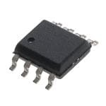
| 描述 | ISOL 3.75KVRMS 1CH UNIDIR SO-8高速光耦合器 Optocouplers 10MBd |
| 产品分类 | |
| 品牌 | Avago Technologies |
| 产品手册 | |
| 产品图片 |
|
| rohs | 符合RoHS无铅 / 符合限制有害物质指令(RoHS)规范要求 |
| 产品系列 | 光耦合器/光电耦合器,高速光耦合器,Avago Technologies ACPL-061L-000E- |
| 数据手册 | http://www.avagotech.com/docs/AV02-3195ENhttp://www.avagotech.com/docs/AV00-0244EN |
| 产品型号 | ACPL-061L-000E |
| PCN封装 | |
| 上升/下降时间(典型值) | 12ns, 12ns |
| 上升时间 | 12 ns |
| 下降时间 | 12 ns |
| 产品种类 | 高速光耦合器 |
| 传播延迟tpLH/tpHL(最大值) | 80ns, 80ns |
| 供应商器件封装 | 8-SO |
| 共模瞬态抗扰度(最小值) | 20kV/µs |
| 其它名称 | 516-2575 |
| 包装 | 管件 |
| 商标 | Avago Technologies |
| 安装类型 | 表面贴装 |
| 封装 | Tube |
| 封装/外壳 | 8-SOIC(0.154",3.90mm 宽) |
| 封装/箱体 | SOIC-8 |
| 工作温度 | -40°C ~ 105°C |
| 工厂包装数量 | 100 |
| 数据速率 | 10 MBd |
| 最大功率耗散 | 20 mW |
| 最大反向二极管电压 | 5 V |
| 最大工作温度 | + 105 C |
| 最大正向二极管电压 | 1.7 V |
| 最大正向二极管电流 | 8 mA |
| 最大连续输出电流 | 10 mA |
| 最小工作温度 | - 40 C |
| 最小正向二极管电压 | 0.95 V |
| 标准包装 | 100 |
| 正向电流 | 8 mA |
| 每芯片的通道数量 | 1 Channel |
| 电压-正向(Vf)(典型值) | 1.3V |
| 电压-电源 | 2.7 V ~ 5.5 V |
| 电压-隔离 | 3750Vrms |
| 电流-DC正向(If) | 8mA |
| 电流-输出/通道 | 10mA |
| 绝缘电压 | 3750 Vrms |
| 输入-输入侧1/输入侧2 | 1/0 |
| 输入类型 | AC/DC |
| 输出类型 | 推挽式/图腾柱 |
| 输出设备 | Photo IC |
| 通道数 | 1 |


- 商务部:美国ITC正式对集成电路等产品启动337调查
- 曝三星4nm工艺存在良率问题 高通将骁龙8 Gen1或转产台积电
- 太阳诱电将投资9.5亿元在常州建新厂生产MLCC 预计2023年完工
- 英特尔发布欧洲新工厂建设计划 深化IDM 2.0 战略
- 台积电先进制程称霸业界 有大客户加持明年业绩稳了
- 达到5530亿美元!SIA预计今年全球半导体销售额将创下新高
- 英特尔拟将自动驾驶子公司Mobileye上市 估值或超500亿美元
- 三星加码芯片和SET,合并消费电子和移动部门,撤换高东真等 CEO
- 三星电子宣布重大人事变动 还合并消费电子和移动部门
- 海关总署:前11个月进口集成电路产品价值2.52万亿元 增长14.8%


PDF Datasheet 数据手册内容提取
ACPL-061L, ACPL-C61L and ACNW261L Ultra Low Power 10 MBd Digital CMOS Optocoupler Data Sheet Description Features The ACPL-061L/ACPL-C61L/ACNW261L is an optically • Ultra low current IDD consumption: 1.5 mA max coupled optocoupler that combines an AlGaAs light • Low input current capability: 1.6 mA min (ACPL-061L), emitting diode and an integrated high gain photo 3 mA min (ACPL-C61L), 4 mA min (ACNW261L) detector addresses the low power need. The optocoupler • Available packages: SO-8, Stretched SO-8 and 400 mil consumes extremely low power, at maximum 1.5 mA IDD widebody per channel across temperature. The forward current is as low as 1.6 mA to 4 mA and allows direct current drive by • Built-in slew-rate controlled output most microprocessors. • Tri-state output with enable pin VE These optocouplers support both 3.3 V and 5 V supply • 20 kV/μs minimum Common Mode Rejection (CMR) at voltage with guaranteed AC and DC operational parame- VCM = 1000 V ters from temperature range -40° C to +105° C. The output • High Speed: 10 MBd min of the detector IC is a CMOS output. An enable input allows the detector output to be strobed. The internal • Guaranteed AC and DC performance over wide Faraday shield provides a guaranteed common mode temperature: -40° C to +105° C transient immunity specification of 20 kV/μs. • Safety and Regulatory Approval The CMOS output is slew-rate controlled and is designed – UL 1577 recognized – 3750 Vrms for 1 minute for to allow the rise time and fall time to be controlled over a ACPL-061L and 5000 Vrms for 1 minute for wide range of the load capacitance. ACPL-C61L/ACNW261L – CSA Approval This unique design provides maximum AC and DC circuit – IEC/EN/DIN EN 60747-5-5 Approval for Reinforced isolation while achieving TTL/CMOS compatibility. These Insulation optocouplers are suitable for high speed logic interfacing, while consuming extremely low power. Applications Functional Diagram • Communication Interface: RS485, CANBus, I2C TRUTH TABLE • Microprocessor System Interfaces NC 1 8 VDD (POSITIVE LOGIC) • Digital isolation for A/D, D/A conversion Anode 2 7 VE LED ENABLE OUTPUT ON H L 6 VO OFF H H Cathode 3 ON L Z NC 4 5 GND OFF L Z Shield ON NC L OFF NC H A 0.1 μF bypass capacitor must be connected between pins VDD and GND CAUTION: It is advised that normal static precautions be taken in handling and assembly of this component to prevent damage and/or degradation which may be induced by ESD. The components featured in this datasheet are not to be used in military or aerospace applications or environments.
Ordering Information ACPL-061L is UL Recognized with 3750 Vrms for 1 minute per UL1577. ACPL-C61L and ACNW261L are UL Recognized with 5000 Vrms for 1 minute per UL1577. Option UL 1577 Surface Tape & 5000 Vrms / IEC/EN/DIN EN Part number (RoHS Compliant) Package Mount Gull Wing Reel 1 Minute rating 60747-5-5 Quantity ACPL-061L -000E SO-8 X 100 per tube -060E X X 100 per tube -500E X X 1500 per reel -560E X X X 1500 per reel ACPL-C61L -000E Stretched X X 80 per tube SO-8 -060E X X X 80 per tube -500E X X X 1000 per reel -560E X X X X 1000 per reel ACNW261L -000E 400 mil X X 42 per tube DIP-8 -300E X X X X 42 per tube -500E X X X X X 750 per reel To order, choose a part number from the part number column and combine with the desired option from the option column to form an order entry. Example 1: ACPL-061L-560E to order product of Small Outline SO-8 package in Tape and Reel packaging with IEC/EN/DIN EN 60747-5-5 Safety Approval in RoHS compliant. Option datasheets are available. Contact your Avago sales representative or authorized distributor for information. 2
Package Outline Drawing ACPL-061L SO-8 Package LAND PATTERN RECOMMENDATION 3.937 ± 0.127 (0.155 ± 0.005) 8 7 6 5 DEVICE PART TEST RATING CODE NNNN Z NUMBER 7.49 (0.295) LEAD-FREE YYWW DATE CODE • EEE LOT ID PIN 1 5.994 ± 0.203 1 2 3 4 (0.236 ± 0.008) 1.9 (0.075) 0.406 ± 0.076 1.270 BSC (0.016 ± 0.003) (0.050) 0.64 (0.025) *5.080 ± 0.127 7° 0.432 45° X (0.200 ± 0.005) (0.017) 3.175 ± 0.127 (0.125 ± 0.005) 0 ~ 7° 0.228 ± 0.025 1.524 (0.009 ± 0.001) (0.060) * Total package length (inclusive of mold flash) 0.203 ± 0.102 (0.008 ± 0.004) 5.207 ± 0.254 (0.205 ± 0.010) 0.305 MIN. (0.012) Notes: Lead coplanarity = 0.10 mm (0.004 inches) max. Floating lead protrusion is 0.15 mm (6 mils) max. Option number 500 not marked Dimensions in Millimeters (Inches) ACPL-C61L Stretched SO-8 Package 5.850±0.254 LAND PATTERN RECOMMENDATION (0.230±0.010) 8 7 6 5 PART NUMBER ROHS-COMPLIANCE INDICATOR DATE CODE 12.650 NNNN Lot ID (0.5) YYWW 6.807±0.127 EEE (0.268±0.005) 1.905 (0.1) 1 2 3 4 1.590±0.127 (0.063±0.005) 7° 0.450 7° 45° (0.018) 3.180±0.127 0.254±0.100 (0.125±0.005) (0.010±0.004) 0.381±0.13 1.270 (0.050) BSG 0.750±0.250 (0.015±0.005) (0.0295±0.010) 11.5±0.250 Dimensions in Millimeters (Inches). (0.453±0.010) Lead coplanarity = 0.1 mm (0.004 inches). 3
ACNW261L 8-Pin Widebody DIP Package 11.23 ± 0.15 11.00 MAX. (0.442 ± 0.006) (0.433) 9.00 ± 0.15 8 7 6 5 (0.354 ± 0.006) AVAGO DEVICE PART NUMBER A TEST RATING CODE NNNNNNNN Z LEAD-FREE • YYWW DATE CODE EEE LOT ID PIN 1 1 2 3 4 10.16 (0.400) TYP. 1.55 (0.061) 7° TYP. + 0.076 MAX. 0.254 - 0.0051 + 0.003) (0.010 - 0.002) 5.10 MAX. (0.201) 3.10 (0.122) 3.90 (0.154) 0.51 (0.021) MIN. 2.54 (0.100) TYP. DIMENSIONS IN MILLIMETERS (INCHES). 1.80 ± 0.15 0.40 (0.016) (0.071 ± 0.006) 0.56 (0.022) NOTE: FLOATING LEAD PROTRUSION IS 0.25 mm (10 mils) MAX. ACNW261L 8-Pin Widebody DIP Package with Gull Wing Surface Mount Option 300E 11.15 ± 0.15 LAND PATTERN RECOMMENDATION (0.442 ± 0.006) 8 7 6 5 13.56 9.00 ± 0.15 (0.534) (0.354 ± 0.006) 1 2 3 4 1.3 2.29 (0.051) (0.09) 1.55 12.30 ± 0.30 MAX. (0.061) (0.484 ± 0.012) 11.00 (0.433)MAX. 0.254 +0.076 - 0.0051 +0.003) (0.010 4.00 - 0.002) MAX. (0.158) 1.78 ± 0.15 1.00 ± 0.15 (0.070 ± 0.006) 2.54 (0.039 ± 0.006) BSC 0.75 ± 0.25 7° NOM. (0.100) (0.030 ± 0.010) Notes: Lead coplanarity = 0.10 mm (0.004 inches) Floating lead protrusion is 0.25 mm (10 mils) max. Dimensions in millimeters (inches) 4
Solder Reflow Profile Recommended reflow condition as per JEDEC Standard, J-STD-020 (latest revision). Non-Halide Flux should be used. Regulatory Information The ACPL-061L, ACPL-C61L, ACNW261L and are pending approval by the following organizations: IEC/EN/DIN EN 60747-5-5 (Option 060E only) UL Approval under UL 1577, component recognition program up to VISO = 3750 VRMS for ACPL-061L and VISO = 5000 VRMS for ACPL-C61L/ACNW261L File E55361. CSA Approval under CSA Component Acceptance Notice #5, File CA 88324. Insulation and Safety Related Specifications Parameter Symbol ACPL-061L ACPL-C61L ACNW261L Unit Conditions Minimum External Air Gap L(101) 4.9 8 9.6 mm Measured from input terminals to (External Clearance) output terminals, shortest distance through air. Minimum External L(102) 4.8 8 10 mm Measured from input terminals to Tracking (External Creepage) output terminals, shortest distance path along body. Minimum Internal Plastic Gap 0.08 0.5 1.0 mm Through insulation distance conductor (Internal Clearance) to conductor, usually the straight line distance thickness between the emitter and detector. Tracking Resistance CTI 175 175 175 V DIN IEC 112/VDE 0303 Part 1 (Comparative Tracking Index) Isolation Group IIIa IIIa IIIa Material Group (DIN VDE 0110, 1/89, Table 1) 5
IEC/EN/DIN EN 60747-5-5 Insulation Characteristics* (Option 060) Characteristic Description Symbol ACPL-061L ACPL-C61L ACNW261L Unit Installation classification per DIN VDE 0110/39, Table 1 for rated mains voltage ≤ 150 Vrms I – IV I – IV I – IV for rated mains voltage ≤ 300 Vrms I – III I – IV I – IV for rated mains voltage ≤ 600 Vrms I – II I – IV I – IV for rated mains voltage ≤ 1000 Vrms I – III I – III Climatic Classification 55/105/21 55/105/21 55/105/21 Pollution Degree (DIN VDE 0110/39) 2 2 2 Maximum Working Insulation Voltage VIORM 567 1414 1414 Vpeak Input to Output Test Voltage, Method b* VPR 1063 2651 2651 Vpeak VIORM x 1.875 = VPR, 100% Production Test with tm = 1 sec, Partial discharge < 5 pC Input to Output Test Voltage, Method a* VPR 907 2262 2262 Vpeak VIORM x 1.6 = VPR, Type and Sample Test, tm = 10 sec, Partial discharge < 5 pC Highest Allowable Overvoltage VIOTM 6000 8000 8000 Vpeak (Transient Overvoltage tini = 60 sec) Safety-limiting values – maximum values allowed in the event of a failure. Case Temperature TS 150 175 150 °C Input Current** IS, INPUT 150 230 400 mA Output Power** PS, OUTPUT 600 600 700 mW Insulation Resistance at TS, VIO = 500 V RS >109 >109 >109 W * Refer to the optocoupler section of the Isolation and Control Components Designer’s Catalog, under Product Safety Regulations section, (IEC/EN/ DIN EN 60747-5-5) for a detailed description of Method a and Method b partial discharge test profiles. ** Refer to the following figure for dependence of PS and IS on ambient temperature. Surface Mount SO-8 Product Surface Mount SSO-8 Product Widebody 400mil DIP-8 Product 1000 700 1000 PS (mW) PS (mW) PS (mW) POWER OUTPUT – P, INPUT CURRENT – ISS246800000000 IS (mA) POWER OUTPUT – P, INPUT CURRENT – ISS462135000000000000 IS (mA) POWER OUTPUT – P, INPUT CURRENT – ISS462135789000000000000000000 IS (mA) 0 0 0 0 25 50 75 100 125 150 175 0 25 50 75 100 125 150 175 200 0 25 50 75 100 125 150 175 TS – CASE TEMPERATURE – °C TS – CASE TEMPERATURE – °C TS – CASE TEMPERATURE – °C 6
Absolute Maximum Ratings Parameter Symbol Min. Max. Units Note Storage Temperature TS -55 125 °C Operating Ambient Temperature TA -40 105 °C Reversed Input Voltage VR 5 V Supply Voltage VDD 6.5 V Average Forward Input Current IF – 8 mA Peak Transient Input Current IF(TRAN) – 1 A < 1 μs Pulse Width, < 300 pulses per second 80 mA < 1 μs Pulse Width, <10% Duty Cycle Output Current IO 10 mA Output Voltage VO -0.5 VDD + 0.5 V Input Power Dissipation PI 14 mW per channel Output Power Dissipation PO 20 mW per channel Lead Solder Temperature TLS 260°C for 10 sec., 1.6 mm below seating plane Solder Reflow Temperature Profile Refer to Solder Reflow Profile section Recommended Operating Conditions Parameter Symbol Part Number Min Max Units Operating Temperature TA -40 105 °C Input Current, Low Level IFL 0 250 μA Input Current, High Level IFH ACPL-061L 1.6 6 mA ACPL-C61L 3 8 mA ACNW261L 4 8 mA Power Supply Voltage VDD 2.7 5.5 V Forward Input Voltage VF (OFF) 0.8 V 7
Electrical Specifications (DC) Over recommended temperature (TA = -40° C to 105° C) and supply voltage (2.7 V ≤ VDD ≤ 5.5 V). All typical specifications are at VDD = 5 V, TA = 25° C. Parameter Symbol Part Number Min Typ Max Units Test Conditions Input Forward Voltage VF ACPL-061L 0.95 1.3 1.7 V IF = 2 mA, Figure 1a, 2a ACPL-C61L 1.2 1.5 1.9 V IF = 5 mA, Figure 1b, 2b ACNW261L 1.2 1.5 1.9 V IF = 5 mA, Figure 1b, 2b Input Reverse BVR ACPL-061L 3 5 V IR = 10 μA Breakdown Voltage ACPL-C61L 7 10 V IR = 10 μA ACNW261L 7 10 V IR = 10 μA Logic High Output Voltage VOH VDD - 0.1 VDD V IF = 0 mA, VI = 0 V, IO = -20 μA VDD - 1.0 VDD V IF = 0 mA, VI = 0 V, IO = -3.2mA Logic Low Output Voltage VOL 0.03 0.1 V IF = 2 mA, VI = 5 V/3.3 V, IO = 20 μA 0.18 0.4 V IF = 2 mA, VI = 5 V/3.3 V, IO = 3.2 mA Input Threshold Current ITH ACPL-061L 0.7 1.3 mA Figure 3a ACPL-C61L 1.5 2.2 mA Figure 3b ACNW261L 1.5 3 mA Figure 3b Logic Low Output Supply IDDL 0.8 1.5 mA Figure 4 Current Logic High Output Supply IDDH 0.8 1.5 mA Figure 5 Current Input Capacitance CIN 60 pF f = 1 MHz, VF = 0 V High Level Enable Current IEH -0.7 -1.6 mA VDD = 5.5 V, VE = 3.0 V Low Level Enable Current [4] IEL -0.9 -1.6 mA VDD = 5.5 V, VE = 0.5 V High Level Enable Voltage [10] VEH 0.7 x VDD V 3.0 V ≤ VDD ≤ 5.5 V Low Level Enable Voltage [10] VEL 0.3 x VDD V 3.0 V ≤ VDD ≤ 5.5 V Input Diode Temperature ΔVF/ΔTA ACPL-061L -1.6 mV/°C IF = 2 mA Coefficient ACPL-C61L -1.9 mV/°C IF = 3 mA ACNW261L -1.9 mV/°C IF = 5 mA 8
Switching Specifications (AC) Over recommended temperature (TA = -40° C to +105° C), supply voltage (2.7 V ≤ VDD ≤ 5.5 V). All typical specifications are at VDD = 5 V, TA = 25° C Parameter Symbol Part Number Min Typ Max Units Test Conditions Propagation Delay Time to tPHL ACPL-061L 46 80 ns IF = 2 mA, VI = 5 V, RT = 1.68 kW, Logic Low Output [1] CL= 15 pF, CMOS Signal Levels. Propagation Delay Time to tPLH 40 80 ns Logic High Output [1] IF = 2 mA, VI = 3.3 V, RT = 870 W, CL= 15 pF, CMOS Signal Levels. Pulse Width tPW 100 ns Figure 6a, 7a Pulse Width Distortion [2] PWD 6 30 ns Propagation Delay Skew [3] tPSK 30 ns Output Rise Time tR 12 ns IF = 2 mA, VI = 5 V, RT = 1.68 kW, (10% – 90%) CL= 15 pF, CMOS Signal Levels. 10 ns IF = 2 mA, VI = 3.3 V, RT = 870 W, CL= 15 pF, CMOS Signal Levels. Output Fall Time tF 12 ns IF = 2 mA, VI = 5 V, RT = 1.68 kW, (90% – 10%) CL= 15 pF, CMOS Signal Levels. 10 ns IF = 2 mA, VI = 3.3 V, RT = 870 W, CL= 15 pF, CMOS Signal Levels. Propagation Delay Time to tPHL ACPL-C61L 47 90 ns IF = 5 mA, VI = 5 V, RT = 680 W, Logic Low Output [1] CL= 15 pF, CMOS Signal Levels. Propagation Delay Time to tPLH 38 90 ns Logic High Output [1] IF = 5 mA, VI = 3.3 V, RT = 340 W, CL= 15 pF, CMOS Signal Levels. Pulse Width tPW 100 ns Figure 6b, 7b Pulse Width Distortion [2] PWD 9 40 ns Propagation Delay Skew [3] tPSK 30 ns Output Rise Time (10% – 90%) tR 12 ns IF = 5 mA, VI = 5 V, RT = 680 Ω, CL= 15 pF, CMOS Signal Levels. 10 ns IF = 5 mA, VI = 3.3 V, RT = 340 Ω, CL= 15 pF, CMOS Signal Levels. Output Fall Time (90% - 10%) tF 12 ns IF = 5 mA, VI = 5 V, RT = 680 Ω, CL= 15 pF, CMOS Signal Levels. 10 ns IF = 5 mA, VI = 3.3 V, RT = 340 Ω, CL= 15 pF, CMOS Signal Levels. Propagation Delay Time tPHL ACNW261L 66 95 ns IF = 5 mA, VI = 5 V, RT = 680 W, to Logic Low Output [1] CL= 15 pF, CMOS Signal Levels. Propagation Delay Time tPLH 47 95 ns IF = 5 mA, VI = 3.3 V, RT = 340 W, to Logic High Output [1] CL= 15 pF, CMOS Signal Levels. Figure 6c, 7c Pulse Width tPW 100 ns Pulse Width Distortion [2] PWD 19 40 ns Propagation Delay Skew [3] tPSK 30 ns Output Rise Time tR 12 ns IF = 5 mA, VI = 5 V, RT = 680 W, (10% – 90%) CL= 15 pF, CMOS Signal Levels. 10 ns IF = 5 mA, VI = 3.3 V, RT = 340 W, CL= 15 pF, CMOS Signal Levels. Output Fall Time tF 12 ns IF = 5 mA, VI = 5 V, RT = 680 W, (90% - 10%) CL= 15 pF, CMOS Signal Levels. 10 ns IF = 5 mA, VI = 3.3 V, RT = 340 W, CL= 15 pF, CMOS Signal Levels. Propagation Delay Time of tELH 9 ns VEL = 0 V, VEH = 3 V, CL= 15 pF Enable from VEH to VEL [5] Figure 8 Propagation Delay Time of tEHL 12 ns Enable from VEL to VEH [6] 9
Switching Specifications (AC) (Continued) Parameter Symbol Part Number Min Typ Max Units Test Conditions Static Common Mode | CMH | ACPL-061L 20 35 kV/μs VCM = 1000 V, TA = 25° C, IF = 0 mA, Transient Immunity at VI = 0V, CL= 15 pF, CMOS Signal Logic High Output [7] Levels. Figure 9 Static Common Mode | CML | 20 35 kV/μs VCM = 1000 V, TA = 25° C, IF = 2 mA, Transient Immunity at VI = 5 V/3.3 V, CL= 15 pF, CMOS Logic Low Output [8] Signal Levels. Figure 9 Dynamic Common Mode CMRD 35 kV/μs VCM = 1000 V, TA = 25° C, IF = 2 mA, Transient Immunity [9] VI = 5 V/3.3 V, 10 MBd data rate, the absolute increase of PWD <10 ns. Figure 9 Static Common Mode | CMH | ACPL-C61L 20 35 kV/μs VCM = 1000 V, TA = 25° C, IF = 0 mA, Transient Immunity at VI = 0 V, CL= 15 pF, CMOS Signal Logic High Output [7] Levels. Figure 9 Static Common Mode | CML | 20 35 kV/μs VCM = 1000 V, TA = 25° C, IF = 5 mA, Transient Immunity at VI = 5 V/3.3 V, CL= 15 pF, CMOS Logic Low Output [8] Signal Levels. Dynamic Common Mode CMRD 35 kV/μs VCM = 1000 V, TA = 25° C, IF = 5 mA, Transient Immunity [9] VI = 5 V/3.3 V, 10 MBd datarate, the absolute increase of PWD <10 ns. Figure 9 Static Common Mode | CMH | ACNW261L 20 35 kV/μs VCM = 1000 V, TA = 25° C, IF = 0 mA, Transient Immunity at VI = 0 V, CL= 15 pF, CMOS Signal Logic High Output [7] Levels. Figure 9 Static Common Mode | CML | 20 35 kV/μs VCM = 1000 V, TA = 25° C, IF = 5 mA, Transient Immunity at VI = 5 V/3.3 V, CL= 15pF, CMOS Logic Low Output [8] Signal Levels. Figure 9 Dynamic Common Mode CMRD 35 kV/μs VCM = 1000 V, TA = 25° C, IF = 5 mA, Transient Immunity [9] VI = 5 V/3.3 V, 10 MBd datarate, the absolute increase of PWD <10 ns. Figure 9 Package Characteristics All typical at TA = 25° C. Parameter Symbol Part Number Min Typ Max Units Test Conditions Input-Output Insulation VISO ACPL-061L 3750 Vrms RH < 50% for 1 min. TA = 25° C ACPL-C61L 5000 ACNW261L Input-Output Resistance RI-O 1012 W VI-O = 500 V Input-Output Capacitance CI-O 0.6 pF f = 1 MHz, TA = 25° C Notes: 1. tPHL propagation delay is measured from the 50% (Vin or IF) on the rising edge of the input pulse to the 50% VDD of the falling edge of the VO signal. tPLH propagation delay is measured from the 50% (Vin or IF) on the falling edge of the input pulse to the 50% level of the rising edge of the VO signal. 2. PWD is defined as |tPHL - tPLH|. 3. tPSK is equal to the magnitude of the worst case difference in tPHL and/or tPLH that will be seen between units at any given temperature within the recommended operating conditions. 4. The JEDEC registration for the ACPL-061L/ACPL-C61L/ACNW261L specifies a maximum IEL of -2.0 mA. Avago guarantees a maximum IEL of -1.6 mA. 5. The tELH enable propagation delay is measured from the 1.5 V point on the falling edge of the enable input pulse to the 1.5 V point on the rising edge of the output pulse. 6. The tEHL enable propagation delay is measured from the 1.5 V point on the rising edge of the enable input pulse to the 1.5 V point on the falling edge of the output pulse. 7. CMH is the maximum tolerable rate of rise of the common mode voltage to assure that the output will remain in a high logic state. 8. CML is the maximum tolerable rate of fall of the common mode voltage to assure that the output will remain in a low logic state. 9. CMD is the maximum tolerable rate of the common mode voltage during data transmission to assure that the absolute increase of the PWD is less than 10 ns. 10. When VE pin is not used, connects VE to VDD will result in improved CMR performance. 10
10 10 A TA = 25° C A m m NT - 1 NT - 1 E E R R R R U U C C D D R R WA 0.1 IF WA 0.1 R R O O F F I - F VF I - F 0.01 0.01 1.1 1.2 1.3 1.4 1.5 1.2 1.3 1.4 1.5 1.6 1.7 VF - FORWARD VOLTAGE - V VF - FORWARD VOLTAGE - V Figure 1a. Typical input diode forward characteristic (ACPL-061L) Figure 1b. Typical input diode forward characteristic (ACPL-C61L/ACNW261L) 1.50 1.7 1.45 1.65 1.40 V E - V1.35 GE - 1.6 G A LTA1.30 OLT1.55 ARD VO11..2205 WARD V 1.5 W R OR1.15 FO1.45 V - FF1.10 V - F 1.4 1.05 1.00 1.35 -40 -20 0 20 40 60 80 100 -40 -20 0 20 40 60 80 100 120 TA - TEMPERATURE - °C TA - TEMPERATURE - °C Figure 2a. Typical VF versus temperature (ACPL-061L) Figure 2b. Typical VF versus temperature (ACPL-C61L/ACNW261L) 1 1.6 A A m m 1.4 RENT - 0.8 RENT - 1.2 R R U U 1 D C 0.6 D C OL OL 0.8 H H RES 0.4 RES 0.6 H H UT T UT T 0.4 NP 0.2 3.3 V NP ITH_3.3 V I - Ith 0 5 V I - Ith 0.20 ITH_5.0 V -40 -20 0 20 40 60 80 100 120 -40 -20 0 20 40 60 80 100 120 TA - TEMPERATURE - °C TA - TEMPERATURE - °C Figure 3a. Typical input threshold current ITH versus temperature Figure 3b. Typical input threshold current ITH versus temperature (ACPL-061L) (ACPL-C61L/ACNW261L) 11
1 1.2 0.9 Y LY PL 1 P 0.8 P P U U S PUT SmA 00..67 TPUT mA 0.8 - LOGIC LOW OUTDLCURRENT - 0000....2345 IDDL _3.3 V - LOGIC HIGH OUDHCURRENT - 000...246 IDDH _3.3 V ID 0.1 IDDL _5.0 V ID IDDH _5.0 V 0 0 -40 -20 0 20 40 60 80 100 120 -40 -20 0 20 40 60 80 100 120 TA - TEMPERATURE - °C TA - TEMPERATURE - °C Figure 4. Typical logic low output supply current IDDL versus temperature Figure 5. Typical logic high output supply current IDDH versus temperature 60 70 t - PROPAGATION DELAY;pWD-PULSE WIDTH DISTORTION - ns 12345000000 TTPPPWHLHDL___555...000 VV V t - PROPAGATION DELAY;pWD-PULSE WIDTH DISTORTION - ns 123456000000 TTPPPWLHHLD___555...000 VV V P-10 P 0 1.5 2 2.5 3 3.5 4 4.5 5 5.5 6 3 4 5 6 7 8 9 IF - PULSE INPUT CURRENT - mA IF - PULSE INPUT CURRENT - mA Figure 6a. Typical switching speed versus pulse input current at 5 V supply Figure 6b. Typical switching speed versus pulse input current at 5 V supply voltage (ACPL-061L) voltage (ACPL-C61L) 80 ns 70 Y;ON - 60 DELAORTI50 PAGATION WIDTH DIST3400 TPHL_5.0 V t - PROpD-PULSE 1200 TPPWLHD__55..00 V V W 0 P -10 3 4 5 6 7 8 9 IF - PULSE INPUT CURRENT -mA Figure 6c. Typical switching speed versus pulse input current at 5 V supply voltage (ACNW261L) 12
60 70 ns 50 ns 60 t - PROPAGATION DELAY;pD-PULSE WIDTH DISTORTION - 123400000 TTPPPWHLHDL___333...333 VV V t - PROPAGATION DELAY;pD-PULSE WIDTH DISTORTION - 1234500000 TTPPPWLHHLD___333...333 VV V W W P P -10 0 1.5 2 2.5 3 3.5 4 4.5 5 5.5 6 3 4 5 6 7 8 9 IF - PULSE INPUT CURRENT -mA IF - PULSE INPUT CURRENT -mA Figure 7a. Typical switching speed versus pulse input current at 3.3 V supply Figure 7b. Typical switching speed versus pulse input current at 3.3 V supply voltage (ACPL-061L) voltage (ACPL-C61L) 80 ns 70 Y;ON - 60 DELAORTI50 t - PROPAGATION pWD-PULSE WIDTH DIST123400000 TTPPPWLHHLD___333...333 VV V OUINTPPVVUUEOTT tEHL tELH 131...505 VVV P -10 3 4 5 6 7 8 9 IF - PULSE INPUT CURRENT -mA Figure 7c. Typical switching speed versus pulse input current at 3.3 V supply Figure 8. Timing diagrams for tEHL and tELH voltage (ACNW261L) 13
Bypassing and PC Board Layout Pulse-width distortion (PWD) results when tPLH and tPHL differ in value. PWD is defined as the difference between The ACPL-061L/ACPL-C61L/ACNW261L optocouplers are tPLH and tPHL and often PWD is defined as the difference extremely easy to use. ACPL-061L/ACPL-C61L/ACNW261L between tPLH and tPHL. This parameter determines the provide CMOS logic output due to the high-speed CMOS maximum data rate capability of a transmission system. IC technology used. PWD can be expressed in percent by dividing the PWD (in ns) by the minimum pulse width (in ns) being transmitted. The external components required for proper operation Typically, PWD in the order of 20-30% of the minimum are the input limiting resistors and the output bypass pulse width is tolerable; the exact figure depends on the capacitor. Capacitor values should be 0.1 μF. particular application (RS232, RS422, T-1, etc.). For each capacitor, the total lead length between both Propagation delay skew, tPSK, is an important parameter ends of the capacitor and the power-supply pins should to consider in parallel data applications where synchroni- not exceed 20 mm. zation of signals on parallel data lines is a concern. If the Propagation Delay, Pulse-Width Distortion and parallel data is being sent through a group of optocou- Propagation Delay Skew plers, differences in propagation delays will cause the data to arrive at the outputs of the optocouplers at different Propagation delay is a figure of merit which describes how times. If this difference in propagation delays is large quickly a logic signal propagates through a system. The enough, it will determine the maximum rate at which propagation delay from low to high (tPLH) is the amount parallel data can be sent through the optocouplers. of time required for an input signal to propagate to the Propagation delay skew is defined as the difference output, causing the output to change from low to high. between the minimum and maximum propagation delays, Similarly, the propagation delay from high to low (tPHL) either tPLH or tPHL, for any given group of optocouplers is the amount of time required for the input signal to which are operating under the same conditions (i.e., the propagate to the output, causing the output to change same supply voltage, output load, and operating temper- from high to low (see Figure 9). ature). As illustrated in Figure 10, if the inputs of a group of optocouplers are switched either ON or OFF at the same RT = R1 + R2, R1/R2 ≈ 1.5 time, tPSK is the difference between the shortest propaga- 1 8 VDD tion delay, either tPLH or tPHL, and the longest propagation R1 IF VI 2 7 VE VI 50% R2 YWWXXX C = 0.1 µF GND1 3 6 VO 2.5 V, VO CMOS 4 5 GND2 tPSK ACPL-061L / ACPL-C61L / ACNW261L VI 50% 3.3V / 5V VDD 1 8 IF Anode C = 0.1µF B 2 7 VE VO 2CM.5O VS, A 6 Figure 10. Propagation delay skew waveform 3 VO Output Cathode Monitoring node 4 Shield 5 GND DATA INPUTS CLOCK Pulse Gen + − VCM VCM(PEAK) VCM 0 V DATA SWITCH AT A: I = 0 mA V VDD F CMH OUTPUTS O V O (min.) tPSK CLOCK SWITCH AT B: I = 2 mA (ACPL-061L) / 5 mA (ACPL-C61L/ACNW261L) F V V O (max.) O GND CML tPSK Figure 9. Recommended printed circuit board layout Figure 11. Parallel data transmission example 14
delay, either tPLH or tPHL. As mentioned earlier, tPSK can This problem is frequently observed in devices with input determine the maximum parallel data transmission rate. high input impedence such as CMOS buffered inputs in either optocoupler or alternate isolator technologies. Figure 10 is the timing diagram of a typical parallel data In some cases, this not only causes momentary missing application with both the clock and the data lines being pulses but in some technologies may even cause input sent through optocouplers. The figure shows data and circuitry to latch-up. clock signals at the inputs and outputs of the optocou- plers. To obtain the maximum data transmission rate, both ACPL-061L/ACPL-C61L/ACNW261L optocoupler family does not face input latch up issue even at very high CMR edges of the clock signal are being used to clock the data; levels, such as those experienced in end equipment level if only one edge were used, the clock signal would need tests (for example IEC61004-4-4) due to the simple diode to be twice as fast. structure of the LED. Propagation delay skew represents the uncertainty of In some cases achieving the rated data sheet CMR perfor- where an edge might be after being sent through an mance levels is not possible in the intended application, optocoupler. Figure 10 shows that there will be uncer- often because of the practical need to actually connect tainty in both the data and the clock lines. It is important the isolator input to the output of a dynamically changing that these two areas of uncertainty not overlap, otherwise signal rather than tying the input statically to VDD1 or the clock signal might arrive before all of the data outputs GND1. have settled, or some of the data outputs may start to change before the clock signal has arrived. This specsmanship issue is often observable with alterna- tive isolators utilizing AC encoding techniques. From these considerations, the absolute minimum pulse To address this requirement for clear transparency on the width that can be sent through optocouplers in a parallel achievable end application performance, the ACPL-061L/ application is twice tPSK. A cautious design should use a ACPL-C61L/ACNW261L series of optocouplers includes an slightly longer pulse width to ensure that any additional un- additional typical performance indication of the dynamic certainty in the rest of the circuit does not cause a problem. CMR in the electrical parameter table. What this informa- The tPSK specified optocouplers offer the advantages of tion indicates is the achievable CMR performance whilst guaranteed specifications for propagation delays, pulse- the input is being toggled on or off during the occurrence width distortion and propagation delay skew over the of a CMR transient. The logic output of the optocoupler recommended temperature, and power supply ranges. is mainly controlled by the level of the LED current due to the short transition rise/fall time of the LED current Optocoupler CMR performance (approximately 10ns), the dynamic noise immunity is essentially the same as the static noise immunity. The principal protection against common mode noise comes down to the fundamental isolation properties of To achieve this goal of meeting the maximum inherent the optocoupler, this in turn is directly related to the input- CMR capabilities of the ACPL-061L/ACPL-C61L/ACNW261L output leakage capacitance of the optocoupler. family, some simple consideration needs to be given to the operation of the LED at the application level. To provide maximum protection to circuitry connected to the input or output of the optocoupler the leakage capac- In particular ensuring that the LED stays either on or off itance is minimized by having large separation distances during a CMR transient. at all points in the optocoupler construction, including Some common design techniques which are sometimes the LED/photodiode interface. used to meet this goal: In addition to the constructional design, additional circuit Keeping LED On: design steps are taking to further mitigate the effects of i) Overdrive the LED with a higher than required forward common mode noise. The most important of these is the use current. of a Faraday shield on the photodetector stage. This faraday Keeping LED Off: shield is effective in optocouplers because the internal modulation frequency (light) is many orders of magnitude i) Reverse bias the LED during the off state. higher than the common mode noise frequency. ii) Minimize the off state impedance across the anode and cathode of the LED during the off state. Application level CMR Performance All these methods are fully capability of enabling the In application, it desirable that the optocoupler’s common full CMR capabilities off the ACPL-061L/ACPL-C61L/ mode isolation perform as close as possible to that ACNW261L family to be achieved. But they do come at the indicated in the data sheets specifications. cost of practical implementation issues or a compromise The first step in meeting this goal is to ensure maintain- on power consumption. ing maximum separation between PCB interconnects on An effective method to meet the goal of maintaining either side of the optocoupler and avoid routing tracks the LED status during a CMR event with no other design beneath the optocoupler. Nonetheless, it is inevitable that compromises other the addition of a single low cost a certain amount of CMR noise will be coupled into the component (resistor). inputs which can potentially result in false-triggering of the input. 15
This CMR optimization method fundamentally makes Table 1 indicates the directions of ILP and ILN flow use of the differential input capability of the LED input. depending on the direction of the common-mode By ensuring the common mode impedance on both the transient. For transients occurring when the LED is on, cathode and anode of the LED are balanced, it effectively common-mode rejection (CML, since the output is in the nullifies the effect of a CMR transient on the LED. This is “low” state) depends upon the amount of LED current most easily achieved by splitting the input bias resistor drive (IF). For conditions where IF is close to the switching into two (as shown in Figure 9). threshold (ITH), CML also depends on the extent which ILP Split resistor configuration for ACPL-061L/ACPL-C61L/ and ILN balance each other. In other words, any condition where common-mode transients cause a momentary ACNW261L decrease in IF (i.e. when dVCM/dt>0 and |IFP| > |IFN|, Figure 12 shows the recommended drive circuit for the referring to Table 1) will cause common-mode failure for ACPL-061L/ACPL-C61L/ACNW261L for optimal common- transients which are fast enough. mode rejection performance. Two LED-current setting Likewise for common-mode transients which occur when resistors are used to balance the common mode impe- the LED is off (i.e. CMH, since the output is “high”), if an dance at LED anode and cathode. Common-mode tran- imbalance between ILP and ILN results in a transient IF sients can capacitively couple from the LED anode (or equal to or greater than the switching threshold of the cathode) to the output-side ground causing current to be optocoupler, the transient “signal” may cause the output shunted away from the LED (which can be bad if the LED to spike below 2 V (which constitutes a CMH failure). is on) or conversely cause current to be injected into the LED (bad if the LED is meant to be off). Figure12 shows the The balanced ILED-setting resistors help equalize the parasitic capacitances which exists between LED anode/ common mode voltage change at anode and cathode cathode and output ground (CLA and CLC). to reduce the amount by which ILED is modulated from transient coupling through CLA and CLC. RT = R1 + R2, R1/R2 ≈ 1.5 1 8 VDD R1 Anode VI 2 7 VE 0.1 µF GND1 R2 3 6 VO Cathode 4 5 GND2 Shie ld Figure 12. Recommended drive circuit for ACPL-061L/ACPL-C61L/ACNW261L for high-CMR 1 8 VDD R1 Anode 2 7 VE 0.1 µF CLA R2 3 6 VO Cathode CLC 4 Shie ld 5 Figure 13. AC equivalent of ACPL-061L/ACPL-C61L/ACNW261L 16
Table 1. Effects of Common Mode Pulse Direction on Transient I LED If |ILP| < |ILN|, If |ILP| > |ILN|, LED IF Current LED IF Current If dVCM/dt Is: then ILP Flows: and ILN Flows: Is Momentarily: Is Momentarily: positive (>0) away from LED away from LED increased decreased anode through CLA cathode through CLC negative (<0) toward LED toward LED decreased increased anode through CLA cathode through CLC Slew-rate controlled output Typically, the output slew rate (rise and fall time) will vary with the output load, as more time is needed to charge up the higher load. The propagation delay and the PWD will increase with the load capacitance. This will be an issue especially in parallel communication because different communication line will have different load capacitances. However, ACPL-061L/ACPL-C61L/ACNW261L has built in slew-rate controlled feature, to ensure that the output rise and fall time remain stable across wide load capacitance. For product information and a complete list of distributors, please go to our web site: www.avagotech.com Avago, Avago Technologies, and the A logo are trademarks of Avago Technologies in the United States and other countries. Data subject to change. Copyright © 2005-2015 Avago Technologies. All rights reserved. AV02-3195EN - August 11, 2015
Mouser Electronics Authorized Distributor Click to View Pricing, Inventory, Delivery & Lifecycle Information: B roadcom Limited: ACPL-061L-000E ACPL-061L-060E ACPL-061L-500E ACPL-061L-560E ACNW261L-000E ACNW261L-300E ACNW261L-500E ACPL-C61L-000E ACPL-C61L-060E ACPL-C61L-500E ACPL-C61L-560E