ICGOO在线商城 > 隔离器 > 光隔离器 - 逻辑输出 > HCPL-7720-000E
 Datasheet下载
- 型号: HCPL-7720-000E
- 制造商: Avago Technologies
- 库位|库存: xxxx|xxxx
- 要求:
| 数量阶梯 | 香港交货 | 国内含税 |
| +xxxx | $xxxx | ¥xxxx |
查看当月历史价格
查看今年历史价格
HCPL-7720-000E产品简介:
ICGOO电子元器件商城为您提供HCPL-7720-000E由Avago Technologies设计生产,在icgoo商城现货销售,并且可以通过原厂、代理商等渠道进行代购。 HCPL-7720-000E价格参考¥35.04-¥35.04。Avago TechnologiesHCPL-7720-000E封装/规格:光隔离器 - 逻辑输出, Logic Output Optoisolator 25MBd Push-Pull, Totem Pole 3750Vrms 1 Channel 10kV/µs CMTI 8-DIP。您可以下载HCPL-7720-000E参考资料、Datasheet数据手册功能说明书,资料中有HCPL-7720-000E 详细功能的应用电路图电压和使用方法及教程。
Broadcom Limited生产的HCPL-7720-000E是一款光隔离器(光电耦合器),属于逻辑输出类别。该型号广泛应用于需要电气隔离和信号传输的场景,其主要应用场景包括:

1. 工业自动化与控制
   - 用于可编程逻辑控制器(PLC)中,实现输入/输出信号的隔离,防止干扰和噪声影响控制系统。
   - 在传感器接口中,提供高电压隔离,确保敏感电路的安全。

2. 电力电子设备
   - 应用于逆变器、变频器和开关电源中,实现主电路与控制电路之间的隔离,保护控制芯片免受高压冲击。
   - 用于电机驱动电路中,将驱动信号与主控芯片隔离,提高系统可靠性。

3. 通信设备
   - 在电信设备中,用于隔离不同电位的信号,防止地环路干扰。
   - 适用于数据传输接口,如RS-485或CAN总线,提供可靠的电气隔离以增强抗噪能力。

4. 医疗设备
   - 用于患者监测设备(如心电图仪)中,确保患者与设备之间无直接电气连接,满足安全标准。
   - 在电源管理模块中,实现高低压电路的隔离,保障设备运行稳定。

5. 汽车电子
   - 应用于车载电子系统中,例如电池管理系统(BMS)、发动机控制单元(ECU)等,提供信号隔离以应对复杂电磁环境。
   - 用于车载网络通信(如LIN、CAN总线),确保信号完整性。

6. 家用电器与消费电子
   - 在智能家电中,用于隔离用户界面与主控板之间的信号,提高安全性。
   - 用于LED驱动电路中,实现低电压控制信号与高电压驱动电路的隔离。

HCPL-7720-000E具有高共模瞬态抗扰度(CMTI)和快速响应时间,适合需要高可靠性和高性能的应用场合。其逻辑输出特性使其易于与数字电路集成,进一步扩展了其应用范围。
| 参数 | 数值 |
| 产品目录 | |
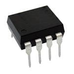
| 描述 | OPTOCOUPLER CMOS 25MBD 8-DIP高速光耦合器 1Ch 10mA 600mW |
| 产品分类 | |
| 品牌 | Avago Technologies |
| 产品手册 | http://www.avagotech.com/docs/AV02-0876EN |
| 产品图片 |
|
| rohs | 符合RoHS无铅 / 符合限制有害物质指令(RoHS)规范要求 |
| 产品系列 | 光耦合器/光电耦合器,高速光耦合器,Avago Technologies HCPL-7720-000E- |
| 数据手册 | http://www.avagotech.com/docs/AV02-0876EN |
| 产品型号 | HCPL-7720-000E |
| PCN封装 | |
| PCN设计/规格 | |
| 上升/下降时间(典型值) | 9ns, 8ns |
| 上升时间 | 9 ns |
| 下降时间 | 8 ns |
| 产品目录绘图 |
|
| 产品目录页面 | |
| 产品种类 | 高速光耦合器 |
| 传播延迟tpLH/tpHL(最大值) | 40ns, 40ns |
| 供应商器件封装 | 8-DIP |
| 共模瞬态抗扰度(最小值) | 10kV/µs |
| 其它名称 | 516-1689-5 |
| 包装 | 管件 |
| 商标 | Avago Technologies |
| 安装类型 | 通孔 |
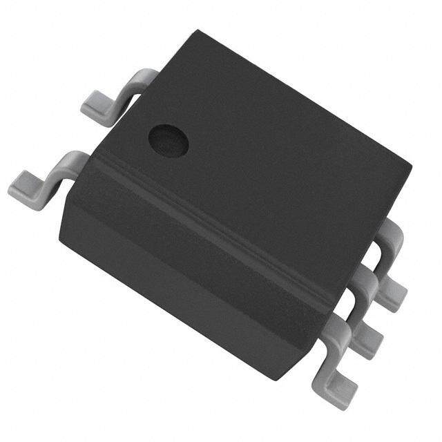
| 封装 | Tube |
| 封装/外壳 | 8-DIP(0.300",7.62mm) |
| 封装/箱体 | PDIP-8 |
| 工作温度 | -40°C ~ 85°C |
| 工厂包装数量 | 50 |
| 数据速率 | 25 MBd |
| 最大功率耗散 | 150 mW |
| 最大工作温度 | + 85 C |
| 最大正向二极管电流 | 10 mA |
| 最大连续输出电流 | 10 mA |
| 最小工作温度 | - 40 C |
| 标准包装 | 50 |
| 每芯片的通道数量 | 1 Channel |
| 电压-正向(Vf)(典型值) | - |
| 电压-电源 | 4.5 V ~ 5.5 V |
| 电压-隔离 | 3750Vrms |
| 电流-DC正向(If) | - |
| 电流-输出/通道 | 10mA |
| 绝缘电压 | 3750 Vrms |
| 输入-输入侧1/输入侧2 | 1/0 |
| 输入类型 | 逻辑 |
| 输出类型 | 推挽式/图腾柱 |
| 输出设备 | Photo IC |
| 通道数 | 1 |


- 商务部:美国ITC正式对集成电路等产品启动337调查
- 曝三星4nm工艺存在良率问题 高通将骁龙8 Gen1或转产台积电
- 太阳诱电将投资9.5亿元在常州建新厂生产MLCC 预计2023年完工
- 英特尔发布欧洲新工厂建设计划 深化IDM 2.0 战略
- 台积电先进制程称霸业界 有大客户加持明年业绩稳了
- 达到5530亿美元!SIA预计今年全球半导体销售额将创下新高
- 英特尔拟将自动驾驶子公司Mobileye上市 估值或超500亿美元
- 三星加码芯片和SET,合并消费电子和移动部门,撤换高东真等 CEO
- 三星电子宣布重大人事变动 还合并消费电子和移动部门
- 海关总署:前11个月进口集成电路产品价值2.52万亿元 增长14.8%
.jpg)


PDF Datasheet 数据手册内容提取
Data Sheet HCPL-0720, HCPL-7720, HCPL-0721, and HCPL-7721 40-ns Propagation Delay, CMOS Optocoupler Description Features Available in either an 8-pin DIP or SO-8 package style +5V CMOS compatibility respectively, the Broadcom® HCPL-772X or HCPL-072X 20-ns max propagation delay skew optocouplers utilize the latest CMOS IC technology to High speed: 25 MBd achieve outstanding performance with very low power 40-ns max propagation delay consumption. The HCPL-772X/072X require only two 10-kV/μs minimum common mode rejection bypass capacitors for complete CMOS compatability. –40 to +85°C temperature range Basic building blocks of the HCPL-772X/072X are a CMOS Safety and regulatory approvals: LED driver IC, a high-speed LED, and a CMOS detector IC. – UL recognized A CMOS logic input signal controls the LED driver IC, which 3750 Vrms for 1 min. per UL 1577 supplies current to the LED. The detector IC incorporates an 5000 Vrms for 1 min. per UL 1577 (for HCPL-772X integrated photodiode, a high-speed transimpedance option 020) amplifier, and a voltage comparator with an output driver. – CSA component acceptance notice #5 – IEC/EN/DIN EN 60747-5-5 VIORM = 630 Vpeak for HCPL-772X option 060 VIORM = 567 Vpeak for HCPL-072X option 060 Applications CAUTION! It is advised that normal static precautions be taken in handling and assembly of this Digital fieldbus isolation: CC-Link, DeviceNet, component to prevent damage and/or PROFIBUS, SDS degradation which may be induced by ESD. AC plasma display panel level shifting The components featured in this data sheet are Multiplexed data transmission not to be used in military or aerospace Computer peripheral interface applications or environments. Microprocessor system interface Broadcom AV02-0876EN October 12, 2017
HCPL-0720, HCPL-7720, HCPL-0721, and HCPL-7721 Data Sheet 40-ns Propagation Delay, CMOS Optocoupler Functional Diagram Truth Table VI Input LED1 VO Output **VDD1 1 8 VDD2** H OFF H L ON L VI 2 7 NC* IO * 3 6 VO LED1 GND1 4 5 GND2 SHIELD * Pin 3 is the anode of the internal LED and must be left unconnected for guaranteed data sheet performance. Pin 7 is not connected internally. ** A 0.01-μF to 0.1-μF bypass capacitor must be connected as close as possible between pins 1 and 4, and 5 and 8. Selection Guide 8-Pin DIP (300 Mil) Small Outline SO-8 Data Rate PWD HCPL-7721 HCPL-0721 25 MB 6 ns HCPL-7720 HCPL-0720 25 MB 8 ns Ordering Information HCPL-0720, HCPL-0721, HCPL-7720, and HCPL-7721 are UL Recognized with 3750 V for 1 minute per UL1577. rms Option RoHS Non RoHS Surface Gull Tape & UL 5000 Vrms/ IEC/EN/DIN Part Number Compliant Compliant Package Mount Wing Reel 1 Minute rating EN 60747-5-5 Quantity HCPL-7720 -000E no option 300 mil 50 per tube HCPL-7721 -300E #300 DIP-8 X X 50 per tube -500E #500 X X X 1000 per reel -020E -020 X 50 per tube -320E -320 X X X 50 per tube -520E -520 X X X X 1000 per reel -060E #060 X 50 per tube -360E #360 X X X 50 per tube -560E #560 X X X X 1000 per reel HCPL-0720 -000E no option SO-8 X X 100 per tube HCPL-0721 -500E #500 X X X 1500 per reel -060E #060 X X X 100 per tube -560E #560 X X X X 1500 per reel Broadcom AV02-0876EN 2
HCPL-0720, HCPL-7720, HCPL-0721, and HCPL-7721 Data Sheet 40-ns Propagation Delay, CMOS Optocoupler To order, choose a part number from the part number column and combine with the desired option from the option column to form an order entry. Example 1: HCPL-7720-560E to order product of Gull Wing Surface Mount package in Tape and Reel packaging with IEC/EN/DIN EN 60747-5-5 Safety Approval and RoHS compliant. Example 2: HCPL-0721 to order product of Small Outline SO-8 package in Tube packaging and non RoHS compliant. Option data sheets are available. Contact your Broadcom sales representative or authorized distributor for information. NOTE: The notation #XXX is used for existing products, while (new) products launched since July 15, 2001 and RoHS compliant will use -XXXE. Package Outline Drawing HCPL-772X 8-Pin DIP Package 9.65 ± 0.25 7.62 ± 0.25 (0.380 ± 0.010) (0.300 ± 0.010) 8 7 6 5 6.35 ± 0.25 DEVICE PART NUMBER (0.250 ± 0.010) AVAGO A NNNN Z TEST RATING CODE • LEAD-FREE YYWW UL LOGO DATE CODE EEE P SPECIAL PROGRAM CODE LOT ID PIN 1 1 2 3 4 1.78 (0.070) MAX. 1.19 (0.047) MAX. + 0.076 5° TYP. 0.254 - 0.051 + 0.003) 3.56 ± 0.13 4.70 (0.185) MAX. (0.010- 0.002) (0.140 ± 0.005) 0.51 (0.020) MIN. 2.92 (0.115) MIN. DIMENSIONS IN MILLIMETERS (INCHES). *MARKING CODE LETTER FOR OPTION NUMBERS "L" = OPTION 020 1.080 ± 0.320 0.65 (0.025) MAX. "V" = OPTION 060 (0.043 ± 0.013) OPTION NUMBERS 300 AND 500 NOT MARKED. 2.54 ± 0.25 (0.100 ± 0.010) NOTE: FLOATING LEAD PROTRUSION IS 0.25 mm (10 mils) MAX. Broadcom AV02-0876EN 3
HCPL-0720, HCPL-7720, HCPL-0721, and HCPL-7721 Data Sheet 40-ns Propagation Delay, CMOS Optocoupler HCPL-772X Package with Gull Wing Surface Mount Option 300 LAND PATTERN RECOMMENDATION 9.65 ± 0.25 1.016 (0.040) (0.380 ± 0.010) 8 7 6 5 6.350 ± 0.25 10.9 (0.430) (0.250 ± 0.010) 1 2 3 4 2.0 (0.080) 1.27 (0.050) 1.780 9.65 ± 0.25 (0.070) (0.380 ± 0.010) 1.19 MAX. (0.047) 7.62 ± 0.25 MAX. (0.300 ± 0.010) + 0.076 0.254 - 0.051 3.56 ± 0.13 + 0.003) (0.140 ± 0.005) (0.010 - 0.002) 1.080 ± 0.320 (0.043 ± 0.013) 0.635 ± 0.25 (0.025 ± 0.010) 12° NOM. 2.54 0.635 ± 0.130 (0.100) (0.025 ± 0.005) BSC DIMENSIONS IN MILLIMETERS (INCHES). LEAD COPLANARITY = 0.10 mm (0.004 INCHES). NOTE: FLOATING LEAD PROTRUSION IS 0.25 mm (10 mils) MAX. HCPL-072X Outline Drawing (Small Outline SO-8 Package) LAND PATTERN RECOMMENDATION 1.91 0.64 (0.075) (0.025) 3.937 ± 0.127 (0.155 ± 0.005) 8 7 6 5 DEVICE PART NNNN Z TEST RATING CODE • NUMBER 3.95 7.49 LEAD-FREE YYWW DATE CODE (0.156) (0.295) EEE LOT ID PIN 1 5.994 ± 0.203 1 2 3 4 (0.236 ± 0.008) 0.406 ± 0.076 1.270BSC 1.27 (0.016 ± 0.003) (0.050) (0.5) *5.080 ± 0.127 7° 0.432 45° X (0.200 ± 0.005) (0.017) 3.175 ± 0.127 (0.125 ± 0.005) 0 ~ 7° 0.228 ± 0.025 1.524 (0.009 ± 0.001) (0.060) * Total package length (inclusive of mold flash) 0.203 ± 0.102 5.207 ± 0.254 (0.205 ± 0.010) 0.305MIN.(0.008 ± 0.004) Dimensions in Millimeters (Inches). (0.012) Note: Floating lead protrusion is 0.15 mm (6 mils) max. Lead coplanarity = 0.10 mm (0.004 inches) max. Option number 500 not marked. Broadcom AV02-0876EN 4
HCPL-0720, HCPL-7720, HCPL-0721, and HCPL-7721 Data Sheet 40-ns Propagation Delay, CMOS Optocoupler Reflow Soldering Profile Recommended reflow condition as per JEDEC Standard, J-STD-020 (latest revision). Non-Halide Flux should be used. Regulatory Information The HCPL-772X/072X have been approved by the following organizations: UL — Recognized under UL1577, component recognition program, File E55361. CSA — Approval under CSA Component Acceptance Notice #5, File CA88324. IEC/EN/DIN EN 60747-5-5 Insulation and Safety Related Specifications Value Parameter Symbol 772X 072X Unit Conditions Minimum External Air Gap L(I01) 7.1 4.9 mm Measured from input terminals to output terminals, (Clearance) shortest distance through air. Minimum External Tracking L(I02) 7.4 4.8 mm Measured from input terminals to output terminals, (Creepage) shortest distance path along body. Minimum Internal Plastic Gap 0.08 0.08 mm Insulation thickness between emitter and detector; (Internal Clearance) also known as distance through insulation. Tracking Resistance CTI ≥175 ≥175 V DIN IEC 112/VDE 0303 Part 1. (Comparative Tracking Index) Isolation Group IIIa IIIa Material Group (DIN VDE 0110, 1/89, Table 1). All Broadcom data sheets report the creepage and clearance inherent to the optocoupler component itself. These dimensions are needed as a starting point for the equipment designer when determining the circuit insulation requirements. However, once mounted on a printed circuit board, minimum creepage and clearance requirements must be met as specified for individual equipment standards. For creepage, the shortest distance path along the surface of a printed circuit board between the solder fillets of the input and output leads must be considered. There are recommended techniques such as grooves and ribs, which may be used on a printed circuit board to achieve desired creepage and clearances. Creepage and clearance distances will also change depending on factors such as pollution degree and insulation level. Broadcom AV02-0876EN 5
HCPL-0720, HCPL-7720, HCPL-0721, and HCPL-7721 Data Sheet 40-ns Propagation Delay, CMOS Optocoupler IEC/EN/DIN EN 60747-5-5 Insulation Characteristics (Option 060) Characteristic HCPL-7720 HCPL-0720 Description Symbol HCPL-7721 HCPL-0721 Unit Installation Classification per DIN VDE 0110/39, Table 1 For Rated Mains Voltage ≤ 150V I – IV I – IV rms For Rated Mains Voltage ≤ 300V I – IV I – III rms For Rated Mains Voltage ≤ 600V I – IV I – III rms Climatic Classification 55/85/21 55/85/21 Pollution Degree (DIN VDE 0110/39) 2 2 Maximum Working Insulation Voltage V 630 567 V IORM peak Input-to-Output Test Voltage, Method ba VPR 1181 1063 Vpeak V x 1.875 = V , 100% Production Test with t = 1s, IORM PR m Partial Discharge < 5 pC Input-to-Output Test Voltage, Method aa VPR 1008 907 Vpeak V x 1.6 = V , Type and Sample Test, t = 10s, IORM PR m Partial Discharge < 5 pC Highest Allowable Overvoltage (Transient Overvoltage, t = 60s) V 8000 6000 V ini IOTM peak Safety-Limiting Values – Maximum Values Allowed in the Event of a Failure Case Temperature T 175 150 °C S Input Current I 230 150 mA S, INPUT Output Power P 600 600 mW S, OUTPUT Insulation Resistance at TS, VIO = 500V RIO ≥109 ≥109 Ω a. Refer to the optocoupler section of the Isolation and Control Component Designer’s Catalog, under Product Safety Regulations section IEC/ EN/DIN EN 60747-5-5, for a detailed description of Method a and Method b partial discharge test profiles. NOTE: These optocouplers are suitable for safe electrical isolation only within the safety limit data. Maintenance of the safety data shall be ensured by means of protective circuits. Absolute Maximum Ratings Parameter Symbol Min. Max. Unit Storage Temperature T –55 125 °C S Ambient Operating Temperaturea TA –40 85 °C Supply Voltages V , V 0 6.0 V DD1 DD2 Input Voltage V –0.5 V + 0.5 V I DD1 Output Voltage V –0.5 V + 0.5 V O DD2 Average Output Current I — 10 mA O Lead Solder Temperature 260°C for 10 sec., 1.6 mm below seating plane. Solder Reflow Temperature Profile See Reflow Soldering Profile section. a. Absolute maximum ambient operating temperature means the device will not be damaged if operated under these conditions. It does not guarantee functionality Broadcom AV02-0876EN 6
HCPL-0720, HCPL-7720, HCPL-0721, and HCPL-7721 Data Sheet 40-ns Propagation Delay, CMOS Optocoupler Recommended Operating Conditions Parameter Symbol Min. Max. Unit Figure Ambient Operating Temperature T –40 85 °C A Supply Voltages V , V 4.5 5.5 V DD1 DD2 Logic High Input Voltage V 2.0 V V 1, 2 IH DD1 Logic Low Input Voltage V 0.0 0.8 V IL Input Signal Rise and Fall Times t , t — 1.0 ms ir if Electrical Specifications (DC) Test conditions that are not specified can be anywhere within the recommended operating range. All typical specifications are at T = +25°C, V = V = +5V. A DD1 DD2 Parameter Symbol Min. Typ. Max. Unit Test Conditions Fig Note Logic Low Input Supply Current I — 6.0 10.0 mA V = 0V a DD1L I Logic High Input Supply Current I — 1.5 3.0 mA V = V a DD1H I DD1 Output Supply Current I — 7.7 9.0 mA DD2L I — 5.8 9.0 mA DD2H Input Current I –10 — 10 μA I Logic High Output Voltage V 4.4 5.0 — V I = –20 μA, V = V 1, 2 OH O I IH 4.0 4.8 — V I = –4 mA, V = V O I IH Logic Low Output Voltage V — 0 0.1 V I = 20 μA, V = V OL O I IL — — 0.1 V I = 400 μA, V = V O I IL — 0.5 1.0 V I = 4 mA, V = V O I IL a. The LED is ON when V is low and OFF when V is high. I I Switching Specifications (AC) Parameter Symbol Min. Typ. Max. Unit Test Conditions Fig. Note Propagation Delay Time to Logic t — 20 40 ns C = 15 pF 3, 6 a PHL L Low Output CMOS Signal Levels Propagation Delay Time to Logic t — 19 40 ns PLH High Output Pulse Width PW 40 — — ns Data Rate — — 25 MBd Pulse Width Distortion |tPHL - tPLH| PWD 7721/0721 3 6 ns 7 b 7720/0720 3 8 ns Propagation Delay Skew t — — 20 c PSK Output Rise Time (10% to 90%) t — 9 ns R Output Fall Time (90% to 10%) t — 8 — ns F Broadcom AV02-0876EN 7
HCPL-0720, HCPL-7720, HCPL-0721, and HCPL-7721 Data Sheet 40-ns Propagation Delay, CMOS Optocoupler Parameter Symbol Min. Typ. Max. Unit Test Conditions Fig. Note Common Mode |CMH| 10 20 — kV/μs VI = VDD1, VO > 0.8 VDD1, d Transient Immunity at Logic High — — — VCM = 1000V VI = 0V, Output VO > 0.8V, VCM = 1000V Common Mode Transient Immunity |CM | 10 20 — L at Logic Low Output Input Dynamic Power Dissipation C — 60 — pF e PD1 Capacitance Output Dynamic Power Dissipation C — 10 — PD2 Capacitance a. t propagation delay is measured from the 50% level on the falling edge of the V signal to the 50% level of the falling edge of the V signal. PHL I O t propagation delay is measured from the 50% level on the rising edge of the V signal to the 50% level of the rising edge of the V signal. PLH I O b. PWD is defined as |t – t |. %PWD (percent pulse width distortion) is equal to the PWD divided by pulse width. PHL PLH c. t is equal to the magnitude of the worst-case difference in t and/or t that will be seen between units at any given temperature within PSK PHL PLH the recommended operating conditions. d. CM is the maximum common mode voltage slew rate that can be sustained while maintaining V > 0.8V . CM is the maximum common H O DD2 L mode voltage slew rate that can be sustained while maintaining V < 0.8V. The common mode voltage slew rates apply to both rising and O falling common mode voltage edges. e. Unloaded dynamic power dissipation is calculated as follows: C × V × f + I × V , where f is switching frequency in MHz. PD DD2 DD DD Package Characteristics Parameter Symbol Min. Typ. Max. Unit Test Conditions Fig. Note Input-Output Momentary –072X VISO 3750 — — Vrms RH ≤ 50%, a, b, c Withstand Voltage t = 1 min, –772X 3750 — — T = 25°C A Option 020 5000 — — Input-Output Resistance RI-O — 1012 — Ω VI-O = 500 Vdc a Input-Output Capacitance C — 0.6 — pF f = 1 MHz I-O Input Capacitance C — 3.0 — d I Input IC Junction-to-Case –772X θ — 145 — °C/W Thermocouple jci Thermal Resistance located at center –072X — 160 — underside of Output IC Junction-to-Case –772X θ — 140 — °C/W jco package Thermal Resistance –072X — 135 — Package Power Dissipation P — — 150 mW PD a. Device considered a two-terminal device: pins 1, 2, 3, and 4 shorted together and pins 5, 6, 7, and 8 shorted together. b. In accordance with UL1577, each HCPL-072X is proof tested by applying an insulation test voltage ≥ 4500 V for 1 second (leakage rms detection current limit, I ≤ 5 μA). Each HCPL-772X is proof tested by applying an insulation test voltage ≥ 4500 V for 1 second (leakage I-O rms detection current limit. I ≤ 5 μA). I-O c. The Input-Output Momentary Withstand Voltage is a dielectric voltage rating that should not be interpreted as an input-output continuous voltage rating. d. C is the capacitance measured at pin 2 (V). I I Broadcom AV02-0876EN 8
HCPL-0720, HCPL-7720, HCPL-0721, and HCPL-7721 Data Sheet 40-ns Propagation Delay, CMOS Optocoupler Figure 1: Typical Output Voltage vs. Input Voltage Figure 2: Typical Input Voltage Switching Threshold vs. Input Supply Voltage 2.2 5 0 °C 2.1 25 °C 0 °C 85 °C 4 25 °C 85 °C 2.0 V (V)O 3 V (V)ITH 1.9 2 1.8 1 1.7 0 1.6 0 1 2 3 4 5 4.5 4.75 5 5.25 5.5 VI (V) VDD1 (V) Figure 3: Typical Propagation Delays vs. Temperature Figure 4: Typical Pulse Width Distortion vs. Temperature 3 29 27 2 25 ns) TPHL s) (PHL 23 D(n , TPLH 21 TPLH PW 1 T 19 17 15 0 0 10 20 30 40 50 60 70 80 0 20 40 60 80 TA (C) Figure 5: Typical Rise Time vs. Temperature Figure 6: Typical Fall Time vs. Temperature 11 7 6 10 5 s) s) n n (R (F T T 4 9 3 8 2 0 20 40 60 80 0 20 40 60 80 TA (C) TA (C) Broadcom AV02-0876EN 9
HCPL-0720, HCPL-7720, HCPL-0721, and HCPL-7721 Data Sheet 40-ns Propagation Delay, CMOS Optocoupler Figure 7: Typical Propagation Delays vs. Output Load Figure 8: Typical Pulse Width Distortion vs. Output Load Capacitance Capacitance 29 6 27 5 25 s) 4 n (L 23 TPHL s) H n TP D( 3 , H 21 PW PL TPLH 2 T 19 17 1 15 0 15 20 25 30 35 40 45 50 15 20 25 30 35 40 45 50 CI (pF) CI (pF) Figure 9: Thermal Derating Curve, Dependence of Safety Limiting Value with Case Temperature per IEC/EN/DIN EN 60747-5-5 S STANDARD 8 PIN DIP PRODUCT S SURFACE MOUNT SO8 PRODUCT – I 800 – I 800 NT PS (mW) NT PS (mW) E 700 E 700 R IS (mA) R IS (mA) R R U 600 U 600 C C T T U 500 U 500 P P N N , IS 400 , IS 400 P P – 300 – 300 R R E(230) E W 200 W 200 O O(150) P P T 100 T 100 U U TP 0 TP 0 U 0 25 50 75 100 125 150 175 200 U 0 25 50 75 100 125 150 175 200 O O TA – CASE TEMPERATURE – °C TA – CASE TEMPERATURE – °C Broadcom AV02-0876EN 10
HCPL-0720, HCPL-7720, HCPL-0721, and HCPL-7721 Data Sheet 40-ns Propagation Delay, CMOS Optocoupler Application Information Bypassing and PC Board Layout The HCPL-772X/072X optocouplers are extremely easy to use. No external interface circuitry is required because the HCPL- 772X/072X use high-speed CMOS IC technology allowing CMOS logic to be connected directly to the inputs and outputs. As shown in Figure10, the only external components required for proper operation are two bypass capacitors. Capacitor values should be between 0.01 μF and 0.1 μF. Each capacitor should be placed as close as possible to the input and output power-supply pins of the optocoupler. Figure 10: Functional Diagram VDD1 1 8 VDD2 C1 C2 VI 2 7 NC NC 3 6 V O GND 4 5 GND 1 2 C1, C2 = 0.01 μF TO 0.1 μF Broadcom AV02-0876EN 11
HCPL-0720, HCPL-7720, HCPL-0721, and HCPL-7721 Data Sheet 40-ns Propagation Delay, CMOS Optocoupler Digital Field Bus Communication Networks To date, despite its many drawbacks, the 4 mA to 20 mA analog current loop has been the most widely accepted standard for implementing process control systems. In today’s manufacturing environment, however, automated systems are expected to help manage the process, not merely monitor it. With the advent of digital field bus communication networks such as CC-Link, DeviceNet, PROFIBUS, and Smart Distributed Systems (SDS), gone are the days of constrained information. Controllers can now receive multiple readings from field devices (sensors, actuators, etc.) in addition to diagnostic information. The physical model for each of these digital field bus communication networks is very similar as shown in Figure11. Each includes one or more buses, an interface unit, optical isolation, transceiver, and sensing and/or actuating devices. Figure 11: Typical Field Bus Communication Physical Model CONTROLLER BUS INTERFACE OPTICAL ISOLATION TRANSCEIVER FIELD BUS TRANSCEIVER TRANSCEIVER TRANSCEIVER TRANSCEIVER OPTICAL OPTICAL OPTICAL OPTICAL ISOLATION ISOLATION ISOLATION ISOLATION BUS BUS BUS BUS INTERFACE INTERFACE INTERFACE INTERFACE XXXXXX SENSOR YYY DEVICE CONFIGURATION MOTOR MOTOR CONTROLLER STARTER Broadcom AV02-0876EN 12
HCPL-0720, HCPL-7720, HCPL-0721, and HCPL-7721 Data Sheet 40-ns Propagation Delay, CMOS Optocoupler Optical Isolation for Field Bus Networks To recognize the full benefits of these networks, Broadcom optocouplers are recommended to provide galvanic isolation. As network communication is bidirectional (involving receiving data from and transmitting data onto the network), two Broadcom optocouplers are needed. By providing galvanic isolation, data integrity is retained via noise reduction and the elimination of false signals. In addition, the network receives maximum protection from power system faults and ground loops. Within an isolated node, such as the DeviceNet Node shown in Figure12, some of the node's components are referenced to a ground other than V– of the network. These components could include such things as devices with serial ports, parallel ports, RS-232 and RS-485 type ports. As shown in Figure12, power from the network is used only for the transceiver and input (network) side of the optocouplers. Isolation of nodes connected to any of the three types of digital field bus networks is best achieved by using the HCPL-772X/ 072X optocouplers. For each network, the HCPL-772X/072X satisify the critical propagation delay and pulse width distortion requirements over the temperature range of 0°C to +85°C, and power supply voltage range of 4.5V to 5.5V. Figure 12: Typical DeviceNet Node AC LINE NODE/APP SPECIFIC LOCAL NODE μP/CAN SUPPLY GALVANIC HCPL HCPL ISOLATION 772x/072x 772x/072x BOUNDARY 5 V REG. TRANSCEIVER DRAIN/SHIELD V+ (SIGNAL) SIGNAL V– (SIGNAL) V+ (POWER) POWER V– (POWER) NETWORK POWER SUPPLY Broadcom AV02-0876EN 13
HCPL-0720, HCPL-7720, HCPL-0721, and HCPL-7721 Data Sheet 40-ns Propagation Delay, CMOS Optocoupler Implementing CC-Link with the HCPL-772X/072X CC-Link (Control and Communication Link) is developed to merge control and information in the low-level network (field network) by PCs, thereby making the multivendor environment a reality. It has data control and message-exchange function, as well as bit control function, and operates at the speed up to 10 Mb/s. The recommended CC-Link circuit is shown in Figure13. Since the HCPL-772X/072X are fully compatible with CMOS logic level signals, the optocoupler is connected directly to the transceiver. Two bypass capacitors (with values between 0.01 μF and 0.1 μF) are required and should be located as close as possible to the input and output power supply pins of the HCPL- 772X/072X. The bypass capacitors are required because of the high-speed digital nature of the signals inside the optocoupler. Figure 13: Recommended CC-Link Application Circuit VDD2 VDD1 SN75ALS181NS (5 V) HCPL-7720#500 (5 V) FIL VCC VCC VDD1 VDD2 10 K DA A R VI VO RD1 DB B RE 0.1 μ 0.1 μ GND1 GND DG DE Y D GND2 GND1 Z GND HCPL-7720#500 GND SLD VDD2 VDD1 VO VI SD 0.1 μ 0.1 μ GND GND FG HCPL-2611#560 VOE NC 1 K VDD + VO MPU 0.1 μ – BOARD HC14 390 OUTPUT GND NC HC14 10 K HCPL-2611#560 VOE NC 1 K VDD + VO 0.1 μ – SDGATEON HC14 390 10 K GND NC HC14 Broadcom AV02-0876EN 14
HCPL-0720, HCPL-7720, HCPL-0721, and HCPL-7721 Data Sheet 40-ns Propagation Delay, CMOS Optocoupler Implementing DeviceNet and SDS with the HCPL-772X/072X With transmission rates up to 1 Mb/s, both DeviceNet and SDS are based upon the same broadcast-oriented, communications protocol: the Controller Area Network (CAN). Three types of isolated nodes are recommended for use on these networks: Isolated Node Powered by the Network (Figure14), Isolated Node with Transceiver Powered by the Network (Figure 19), and Isolated Node Providing Power to the Network (Figure16). Isolated Node Powered by the Network This type of node is very flexible and as can be seen in Figure14, is regarded as isolated because not all of its components have the same ground reference. Yet, all components are still powered by the network. This node contains two regulators: one is isolated and powers the CAN controller, node-specific application and isolated (node) side of the two optocouplers while the other is non-isolated. The non-isolated regulator supplies the transceiver and the non-isolated (network) half of the two optocouplers. Figure 14: Isolated Node Powered by the Network NODE/APP SPECIFIC μP/CAN ISOLATED GALVANIC HCPL HCPL SWITCHING ISOLATION 772x/072x 772x/072x POWER BOUNDARY SUPPLY REG. TRANSCEIVER DRAIN/SHIELD V+ (SIGNAL) SIGNAL V– (SIGNAL) V+ (POWER) POWER V– (POWER) NETWORK POWER SUPPLY Broadcom AV02-0876EN 15
HCPL-0720, HCPL-7720, HCPL-0721, and HCPL-7721 Data Sheet 40-ns Propagation Delay, CMOS Optocoupler Isolated Node with Transceiver Powered by the Network Figure15 shows a node powered by both the network and another source. In this case, the transceiver and isolated (network) side of the two optocouplers are powered by the network. The rest of the node is powered by the AC line which is very beneficial when an application requires a significant amount of power. This method is also desirable as it does not heavily load the network. More importantly, the unique dual-inverting design of the HCPL-772X/072X ensure the network will not lock- up if either AC line power to the node is lost or the node powered-off. Specifically, when input power (V ) to the HCPL-772X/072X located DD1 in the transmit path is eliminated, a RECESSIVE bus state is ensured as the HCPL-772X/ 072X output voltage (V ) go HIGH. O Bus V+ Sensing* It is suggested that the Bus V+ sense block shown in Figure15 be implemented. A locally powered node with an unpowered isolated Physical Layer will accumulate errors and become bus-off if it attempts to transmit. The Bus V+ sense signal would be used to change the BOI attribute of the DeviceNet Object to the auto-reset (01) value. Refer to Volume 1, Section 5.5.3. This would cause the node to continually reset until bus power was detected. Once power was detected, the BOI attribute would be returned to the hold in bus-off (00) value. The BOI attribute should not be left in the auto-reset (01) value since this defeats the jabber protection capability of the CAN error confinement. Any inexpensive low-frequency optical isolator can be used to implement this feature. Figure 15: Isolated Node with Transceiver Powered by the Network AC LINE NON ISO NODE/APP SPECIFIC 5 V μP/CAN GALVANIC HCPL HCPL *HCPL ISOLATION 772x/072x 772x/072x 772x/072x BOUNDARY REG. TRANSCEIVER DRAIN/SHIELD V+ (SIGNAL) SIGNAL V– (SIGNAL) V+ (POWER) POWER V– (POWER) NETWORK * OPTIONAL FOR BUS V + SENSE POWER SUPPLY Broadcom AV02-0876EN 16
HCPL-0720, HCPL-7720, HCPL-0721, and HCPL-7721 Data Sheet 40-ns Propagation Delay, CMOS Optocoupler Isolated Node Providing Power to the Network Figure16 shows a node providing power to the network. The AC line powers a regulator which provides 5V locally. The AC line also powers a 24V isolated supply, which powers the network, and another 5V regulator, which, in turn, powers the transceiver and isolated (network) side of the two optocouplers. This method is recommended when there is a limited number of devices on the network, which do not require much power, thus eliminating the need for separate power supplies. More importantly, the unique dual-inverting design of the HCPL-772X/072X ensure the network will not lock- up if either AC line power to the node is lost or the node powered-off. Specifically, when input power (V ) to the HCPL-772X/072X located DD1 in the transmit path is eliminated, a RECESSIVE bus state is ensured as the HCPL-772X/ 072X output voltage (V ) go HIGH. O Figure 16: Isolated Node Providing Power to the Network AC LINE DeviceNet Node NODE/APP SPECIFIC 5 V REG. μP/CAN ISOLATED GALVANIC HCPL HCPL SWITCHING ISOLATION 772x/072x 772x/072x POWER BOUNDARY SUPPLY 5 V REG. TRANSCEIVER DRAIN/SHIELD V+ (SIGNAL) SIGNAL V– (SIGNAL) V+ (POWER) POWER V– (POWER) The recommended DeviceNet application circuit is shown in Figure17. Since the HCPL-772X/072X are fully compatible with CMOS logic level signals, the optocoupler is connected directly to the CAN transceiver. Two bypass capacitors (with values between 0.01 µF and 0.1 µF) are required and should be located as close as possible to the input and output power-supply pins of the HCPL-772X/072X. The bypass capacitors are required because of the high-speed digital nature of the signals inside the optocoupler. Broadcom AV02-0876EN 17
HCPL-0720, HCPL-7720, HCPL-0721, and HCPL-7721 Data Sheet 40-ns Propagation Delay, CMOS Optocoupler Figure 17: Recommended DeviceNet Application Circuit GALVANIC ISOLATION ISO 5 V BOUNDARY 5 V LINEAR OR 1 VDD1 VDD2 8 SWITCHING REGULATOR TX0 0.01 + + 2 VIN 7 μF HCPL-772x VCC 5 V+ 0.01 μF 3 HCPL-072x VO 6 TxD CANH 4 CAN+ 4 GND1 GND2 5 + 82C250 3 SHIELD C4 0.01 μF CANL 2 CAN– GND Rs REF 1 V– VREF RXD 5 GND2 GND1 4 GND C1 RX0 6 VO 3 0μ.0F1 3D01 V 0.01 μF R1 1M 500 V HCPL-772x 0.01 μF 7 HCPL-072x VIN 2 8 VDD2 VDD1 1 ISO 5 V 5 V Broadcom AV02-0876EN 18
HCPL-0720, HCPL-7720, HCPL-0721, and HCPL-7721 Data Sheet 40-ns Propagation Delay, CMOS Optocoupler Implementing PROFIBUS with the HCPL-772X/072X An acronym for Process Fieldbus, PROFIBUS is essentially a twisted-pair serial link very similar to RS-485 capable of achieving high-speed communication up to 12 MBd. As shown in Figure18, a PROFIBUS Controller (PBC) establishes the connection of a field automation unit (control or central processing station) or a field device to the transmission medium. The PBC consists of the line transceiver, optical isolation, frame character transmitter/receiver (UART), and the FDL/APP processor with the interface to the PROFIBUS user. Figure 18: PROFIBUS Controller (PBC) PROFIBUS USER: CONTROL STATION (CENTRAL PROCESSING) OR FIELD DEVICE USER INTERFACE FDL/APP PROCESSOR UART PBC OPTICAL ISOLATION TRANSCEIVER MEDIUM The recommended PROFIBUS application circuit is shown in Figure19. Since the HCPL-772X/072X are fully compatible with CMOS logic level signals, the optocoupler is connected directly to the transceiver. Two bypass capacitors (with values between 0.01 μF and 0.1 μF) are required and should be located as close as possible to the input and output power-supply pins of the HCPL-772X/072X. The bypass capacitors are required because of the high-speed digital nature of the signals inside the optocoupler. Being very similar to multistation RS485 systems, the HCPL-061N optocoupler provides a transmit disable function which is necessary to make the bus free after each master/slave transmission cycle. Specifically, the HCPL-061N disables the transmitter of the line driver by putting it into a high state mode. In addition, the HCPL-061N switches the RX/TX driver IC into the listen mode. The HCPL-061N offers HCMOS compatibility and the high CMR performance (1 kV/μs at V = 1000V) CM essential in industrial communication interfaces. Broadcom AV02-0876EN 19
HCPL-0720, HCPL-7720, HCPL-0721, and HCPL-7721 Data Sheet 40-ns Propagation Delay, CMOS Optocoupler Figure 19: Recommended PROFIBUS Application Circuit GALVANIC ISOLATION BOUNDARY 5 V ISO 5 V 8 VDD2 VDD1 1 ISO 5 V 0.01 μF 7 VIN 2 8 HCPL-772x 0.01 1 VCC Rx 6 VO HCPL-072x 3 μF R A 6 + 0.01 5 GND2 GND1 4 μF SN75176B RT SHIELD 4 7 D B – 3 DE 5 V ISO 5 V 2 RE 1 VDD1 VDD2 8 GND 5 0.01 0.01 μF 1 M Tx 2 VIN 7 μF HCPL-772x 0.01 μF 3 HCPL-072x VO 6 4 GND1 GND2 5 ISO 5 V 1 VCC 8 5 V 2 ANODE VE 7 680 Ω 0.01 HCPL-061N 1, 0 kΩ μF Tx ENABLE 3 CATHODE VO 6 4 GND 5 Broadcom AV02-0876EN 20
Broadcom, the pulse logo, Connecting everything, Avago Technologies, Avago, and the A logo are among the trademarks of Broadcom and/or its affiliates in the United States, certain other countries and/or the EU. Copyright © 2017 by Broadcom. All Rights Reserved. The term “Broadcom” refers to Broadcom Limited and/or its subsidiaries. For more information, please visit www.broadcom.com. Broadcom reserves the right to make changes without further notice to any products or data herein to improve reliability, function, or design. Information furnished by Broadcom is believed to be accurate and reliable. However, Broadcom does not assume any liability arising out of the application or use of this information, nor the application or use of any product or circuit described herein, neither does it convey any license under its patent rights nor the rights of others.
Mouser Electronics Authorized Distributor Click to View Pricing, Inventory, Delivery & Lifecycle Information: B roadcom Limited: HCPL-0720 HCPL-0720#060 HCPL-0720#500 HCPL-0720#560 HCPL-0720-000E HCPL-0720-060E HCPL-0720- 500E HCPL-0720-560E HCPL-0721 HCPL-0721#060 HCPL-0721#500 HCPL-0721#560 HCPL-0721-000E HCPL- 0721-060E HCPL-0721-500E HCPL-0721-560E HCPL-7720 HCPL-7720#060 HCPL-7720#300 HCPL-7720#360 HCPL-7720#500 HCPL-7720#560 HCPL-7720-000E HCPL-7720-020 HCPL-7720-020E HCPL-7720-060E HCPL- 7720-300E HCPL-7720-320 HCPL-7720-320E HCPL-7720-360E HCPL-7720-500E HCPL-7720-520 HCPL-7720- 520E HCPL-7720-560E HCPL-7721 HCPL-7721#060 HCPL-7721#300 HCPL-7721#360 HCPL-7721#500 HCPL- 7721#560 HCPL-7721-000E HCPL-7721-020 HCPL-7721-020E HCPL-7721-060E HCPL-7721-300E HCPL-7721- 320 HCPL-7721-320E HCPL-7721-360E HCPL-7721-500E HCPL-7721-520 HCPL-7721-520E HCPL-7721-560E