ICGOO在线商城 > 隔离器 > 光隔离器 - 逻辑输出 > FOD0720R2
 Datasheet下载
- 型号: FOD0720R2
- 制造商: Fairchild Semiconductor
- 库位|库存: xxxx|xxxx
- 要求:
| 数量阶梯 | 香港交货 | 国内含税 |
| +xxxx | $xxxx | ¥xxxx |
查看当月历史价格
查看今年历史价格
FOD0720R2产品简介:
ICGOO电子元器件商城为您提供FOD0720R2由Fairchild Semiconductor设计生产,在icgoo商城现货销售,并且可以通过原厂、代理商等渠道进行代购。 FOD0720R2价格参考。Fairchild SemiconductorFOD0720R2封装/规格:光隔离器 - 逻辑输出, Logic Output Optoisolator 25Mbps Push-Pull, Totem Pole 3750Vrms 1 Channel 20kV/µs CMTI 8-SOIC。您可以下载FOD0720R2参考资料、Datasheet数据手册功能说明书,资料中有FOD0720R2 详细功能的应用电路图电压和使用方法及教程。
FOD0720R2 是安森美半导体(ON Semiconductor)生产的一款光隔离器,属于光耦合器的一种,具有逻辑输出功能。该器件常用于需要电气隔离的电路中,以保护系统和用户免受高压或高电压瞬态的影响。

FOD0720R2 的主要应用场景包括:

1. 工业控制系统:用于PLC(可编程逻辑控制器)、工业自动化设备中,实现输入/输出信号的电气隔离,提升系统抗干扰能力和安全性。

2. 电源管理与转换设备:应用于开关电源、DC-DC转换器、UPS(不间断电源)等设备中,用于隔离控制信号,防止高压侧对低压控制电路的干扰或损坏。

3. 电机驱动与变频器:在电机控制和变频调速系统中,实现控制电路与功率电路之间的信号隔离,保障控制芯片安全。

4. 通信接口隔离:在RS-485、CAN等工业通信总线接口中使用,防止地电位差造成的通信干扰或设备损坏。

5. 医疗电子设备:用于需要高安全标准的医疗仪器中,实现病人与设备之间、设备与大地之间的电气隔离,符合医疗安全规范。

FOD0720R2具有高速响应、高隔离电压、抗干扰能力强等特点,适用于多种需要信号隔离和系统保护的场合。
| 参数 | 数值 |
| 产品目录 | |
| 描述 | OPTOCOUPLER 25MBIT SEC 8-SOIC |
| 产品分类 | |
| 品牌 | Fairchild Semiconductor |
| 数据手册 | |
| 产品图片 |
|
| 产品型号 | FOD0720R2 |
| rohs | 无铅 / 符合限制有害物质指令(RoHS)规范要求 |
| 产品系列 | OPTOPLANAR® |
| 上升/下降时间(典型值) | 5ns, 4.5ns |
| 传播延迟tpLH/tpHL(最大值) | 40ns, 40ns |
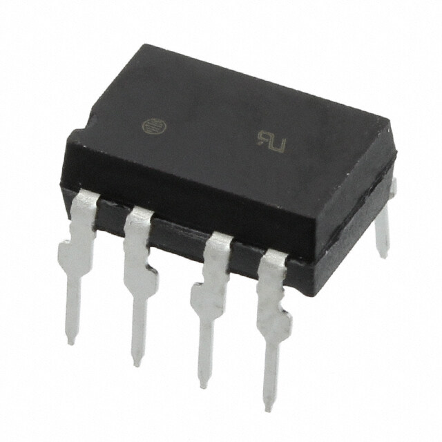
| 供应商器件封装 | 8-SO |
| 共模瞬态抗扰度(最小值) | 20kV/µs |
| 其它名称 | FOD0720R2CT |
| 包装 | 剪切带 (CT) |
| 安装类型 | 表面贴装 |
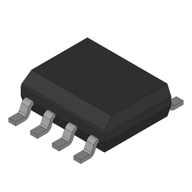
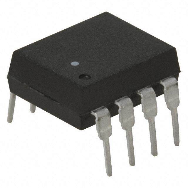
| 封装/外壳 | 8-SOIC(0.154",3.90mm 宽) |
| 工作温度 | -40°C ~ 100°C |
| 数据速率 | 25Mbps |
| 标准包装 | 1 |
| 电压-正向(Vf)(典型值) | - |
| 电压-电源 | 4.5 V ~ 5.5 V |
| 电压-隔离 | 3750Vrms |
| 电流-DC正向(If) | - |
| 电流-输出/通道 | 10mA |
| 输入-输入侧1/输入侧2 | 1/0 |
| 输入类型 | 逻辑 |
| 输出类型 | 推挽式/图腾柱 |
| 通道数 | 1 |


- 商务部:美国ITC正式对集成电路等产品启动337调查
- 曝三星4nm工艺存在良率问题 高通将骁龙8 Gen1或转产台积电
- 太阳诱电将投资9.5亿元在常州建新厂生产MLCC 预计2023年完工
- 英特尔发布欧洲新工厂建设计划 深化IDM 2.0 战略
- 台积电先进制程称霸业界 有大客户加持明年业绩稳了
- 达到5530亿美元!SIA预计今年全球半导体销售额将创下新高
- 英特尔拟将自动驾驶子公司Mobileye上市 估值或超500亿美元
- 三星加码芯片和SET,合并消费电子和移动部门,撤换高东真等 CEO
- 三星电子宣布重大人事变动 还合并消费电子和移动部门
- 海关总署:前11个月进口集成电路产品价值2.52万亿元 增长14.8%

.jpg)


PDF Datasheet 数据手册内容提取
Is Now Part of To learn more about ON Semiconductor, please visit our website at www.onsemi.com Please note: As part of the Fairchild Semiconductor integration, some of the Fairchild orderable part numbers will need to change in order to meet ON Semiconductor’s system requirements. Since the ON Semiconductor product management systems do not have the ability to manage part nomenclature that utilizes an underscore (_), the underscore (_) in the Fairchild part numbers will be changed to a dash (-). This document may contain device numbers with an underscore (_). Please check the ON Semiconductor website to verify the updated device numbers. The most current and up-to-date ordering information can be found at www.onsemi.com. Please email any questions regarding the system integration to Fairchild_questions@onsemi.com. ON Semiconductor and the ON Semiconductor logo are trademarks of Semiconductor Components Industries, LLC dba ON Semiconductor or its subsidiaries in the United States and/or other countries. ON Semiconductor owns the rights to a number of patents, trademarks, copyrights, trade secrets, and other intellectual property. A listing of ON Semiconductor’s product/patent coverage may be accessed at www.onsemi.com/site/pdf/Patent-Marking.pdf. ON Semiconductor reserves the right to make changes without further notice to any products herein. ON Semiconductor makes no warranty, representation or guarantee regarding the suitability of its products for any particular purpose, nor does ON Semiconductor assume any liability arising out of the application or use of any product or circuit, and specifically disclaims any and all liability, including without limitation special, consequential or incidental damages. Buyer is responsible for its products and applications using ON Semiconductor products, including compliance with all laws, regulations and safety requirements or standards, regardless of any support or applications information provided by ON Semiconductor. “Typical” parameters which may be provided in ON Semiconductor data sheets and/or specifications can and do vary in different applications and actual performance may vary over time. All operating parameters, including “Typicals” must be validated for each customer application by customer’s technical experts. ON Semiconductor does not convey any license under its patent rights nor the rights of others. ON Semiconductor products are not designed, intended, or authorized for use as a critical component in life support systems or any FDA Class 3 medical devices or medical devices with a same or similar classification in a foreign jurisdiction or any devices intended for implantation in the human body. Should Buyer purchase or use ON Semiconductor products for any such unintended or unauthorized application, Buyer shall indemnify and hold ON Semiconductor and its officers, employees, subsidiaries, affiliates, and distributors harmless against all claims, costs, damages, and expenses, and reasonable attorney fees arising out of, directly or indirectly, any claim of personal injury or death associated with such unintended or unauthorized use, even if such claim alleges that ON Semiconductor was negligent regarding the design or manufacture of the part. ON Semiconductor is an Equal Opportunity/Affirmative Action Employer. This literature is subject to all applicable copyright laws and is not for resale in any manner.
F O D 0 December 2010 7 2 1 , F O FOD0721, FOD0720, FOD0710 D 0 High CMR, 25Mbit/sec Logic Gate Optocoupler 7 2 0 , F Features Description O D ■ 20kV/µs minimum CMR The FOD0721/0720/0710 family utilizes Fairchild’s 0 7 ■ 40ns max. propagation delay proprietary coplanar packaging technology, Optoplanar®, 1 0 ■ Data Rate, Non-Return Zero Coding and optimized IC design to guarantee minimum 20kV/µs — Common Mode Noise Rejection (CMR) rating. – 25Mbit/sec (FOD0721 and FOD0720) H – 12.5Mbit/sec (FOD0710) These high-speed logic gate optocouplers consist of a i g ■ Pulse Width Distortion high-speed AlGaAs LED driven by a CMOS IC coupled h – 6ns (FOD0721) to a CMOS detector IC, comprising an integrated photo- C diode, a high-speed transimpedance amplifier and a M – 8ns (FOD0720 and FOD0710) voltage comparator with an output driver. The CMOS R ■ +5V CMOS compatibility technology coupled to the high efficiency of the LED , 2 ■ Extended industrial temperate range achieves low power consumption as well as very high 5 M – -40 to 100°C temperature range speed (40ns propagation delay, 6ns pulse width b ■ Safety and regulatory approvals distortion). i t / – UL1577, 3750 VACrms for 1 min. (File #E90700, These devices are available in a compact 8-pin small se Volume 2) outline package. c – IEC60747-5-2 pending approval L o g Applications i c G ■ Industrial fieldbus communications a – Profibus, DeviceNet, CAN, RS485 t e ■ Programmable logic control O ■ Isolated data acquisition system p t o c o Functional Schematic u p l e r VDD1 1 8 VDD2 VI 2 7 NC * 3 6 VO GND1 4 5 GND2 *: Pin 3 must be left unconnected Truth Table VI LED VO H OFF H L ON L ©2004 Fairchild Semiconductor Corporation www.fairchildsemi.com FOD0721, FOD0720, FOD0710 Rev. 1.0.9
F O Pin Definitions D 0 7 Pin Number Pin Name Pin Function Description 2 1 1 VDD1 Input Supply Voltage , F 2 V Input Data O I D 3 LED Anode – must be left unconnected 0 7 4 GND1 Input Ground 2 0 5 GND2 Output Ground , F 6 V Output Data O O D 7 NC Not Connected 0 7 8 V Output Supply Voltage 1 DD2 0 — H Absolute Maximum Ratings (TA = 25°C unless otherwise specified.) ig Stresses exceeding the absolute maximum ratings may damage the device. The device may not function or be h operable above the recommended operating conditions and stressing the parts to these levels is not recommended. C In addition, extended exposure to stresses above the recommended operating conditions may affect device reliability. M R The absolute maximum ratings are stress ratings only. , 2 Symbol Parameter Value Units 5 M T Storage Temperature -40 to +125 °C b STG i t T Operating Temperature -40 to +100 °C / OPR s e TSOL Lead Solder Temperature 260 for 10 sec °C c L Reflow Temperature Profile (Refer to Relow Profile) o g V Input Supply Voltage 0 to 6.0 V DD1 i c VI Input Voltage -0.5 to VDD1 + 0.5 V G a I Input DC Current -10 to +10 mA I t e VDD2 Output Supply Voltage 0 to 6.0 V O p V Output Voltage -0.5 to V + 0.5 V D DD2 t o I Average Output Current 10 mA c O o PD1 Input Power Dissipation 90 mW u p PD2 Output Power Dissipation 70 mW le r Recommended Operating Conditions The Recommended Operating Conditions table defines the conditions for actual device operation. Recommended operating conditions are specified to ensure optimal performance to the datasheet specifications. Fairchild does not recommend exceeding them or designing to absolute maximum ratings. Symbol Parameter Min. Max. Unit T Ambient Operating Temperature -40 +100 °C OPR V , V Supply Voltages 4.5 5.5 V DD1 DD2 V Logic High Input Voltage 2.0 V V IH DD1 V Logic Low Input Voltage 0 0.8 V IL t , t Input Signal Rise and Fall Time 1.0 ms r f • A 0.1µF bypass capacitor must be connected between pins 1 and 4, and 5 and 8 • Pin 3 must be left unconnected ©2004 Fairchild Semiconductor Corporation www.fairchildsemi.com FOD0721, FOD0720, FOD0710 Rev. 1.0.9 2
F O Electrical Characteristics (T = -40°C to 100°C and 4.5V ≤ V ≤ 5.5V, all typicals are at T = 25°C, V = 5V) D A DD A DD 0 7 Symbol Parameter Test Conditions Min. Typ. Max. Unit 2 1 INPUT CHARACTERISTICS , F I Logic Low Input Supply Current V = 0V 6.5 10.0 mA O DD1L I D IDD1H Logic High Input Supply Current VI = VDD1 0.8 3.0 mA 0 7 IDD1 Input Supply Current 13.0 mA 2 0 II Input Current -10 +10 µA , F OUTPUT CHARACTERISTICS O D IDD2L Logic Low Output Supply Current VI = 0V 5.5 9 mA 0 7 I Logic High Output Supply Current V = V 5.3 9 mA 1 DD2H I DD1 0 VOH Logic High Output Voltage IO = -20µA, VI = VIH 4.4 5.0 V — VOH IO = -4mA, VI = VIH 4.0 4.8 V H i V Logic Low Output Voltage I = 20µA, V = V 0 0.1 V g OL O I IL h VOL IO = 4mA, VI = VIL 0.5 1.0 V C M R Isolation Characteristics (TA = -40°C to +100°C unless otherwise specified.) , 2 5 Symbol Characteristics Test Conditions Min. Typ.* Max. Unit M b VISO Input-Output Isolation Voltage f = 60Hz, t = 1.0 min, II-O ≤ 10µA(1)(2) 3750 VacRMS it / R Isolation Resistance V = 500V(1) 1011 Ω s ISO I-O e CISO Isolation Capacitance VI-O = 0 , f = 1.0MHz(1) 0.2 pF c L *All typicals at T = 25°C o A g i Notes: c 1. Device is considered a two terminal device: Pins 1, 2, 3 and 4 are shorted together and Pins 5, 6, 7 and 8 are shorted G a together. t e 2. 3,750 VAC RMS for 1 minute duration is equivalent to 4,500 VAC RMS for 1 second duration. O p t o c o u p l e r ©2004 Fairchild Semiconductor Corporation www.fairchildsemi.com FOD0721, FOD0720, FOD0710 Rev. 1.0.9 3
F O Switching Characteristics (T = -40°C to 100°C and 4.5V ≤ V ≤ 5.5V, all typicals are at T = 25°C, V = 5V) D A DD A DD 0 7 Symbol Parameter Test Conditions Min. Typ. Max. Unit 2 1 tPHL Propagation Delay Time to CL = 15pF 21 40 ns , F Logic Low Output O t Propagation Delay Time to C = 15pF 23 40 ns D PLH L 0 Logic High Output 7 2 PWD Pulse Width Distortion, | t – t | 0 PHL PLH , FOD0710 PW = 80ns, C = 15pF 2 8 ns F L O FOD0720 PW = 40ns, C = 15pF 2 8 ns D L 0 FOD0721 PW = 40ns, C = 15pF 2 6 ns 7 L 1 Data Rate FOD0710 12.5 Mb/s 0 — FOD0720, FOD0721 25 Mb/s H tPSK Propagation Delay Skew CL = 15pF(3) 20 ns ig t Output Rise Time (10%–90%) 5 ns h R C tF Output Fall Time (90%–10%) 4.5 ns M |CM | Common Mode Transient V = V , V > 0.8 V 20 40 kV/µs R H Immunity at Output High VICM =D 1D0100VO(4) DD2 , 2 5 |CM | Common Mode Transient V = 0V, V < 0.8, 20 40 kV/µs M L I O Immunity at Output Low V = 1000V(4) b CM i t / Notes: s e 3. t is equal to the magnitude of the worst case difference in t and/or t that will be seen between units at any given c PSK PHL PLH temperature within the recommended operating conditions. L o 4. Common mode transient immunity at output high is the maximum tolerable (positive) dVcm/dt on the leading edge g i of the common mode impulse signal. Vcm, to assure that the output will remain high. Common mode transient c immunity at output low is the maximum tolerable (negative dVcm/dt on the trailing edge of the common pulse G signal, Vcm, to assure that the output will remain low. a t e O p t o c o u p l e r ©2004 Fairchild Semiconductor Corporation www.fairchildsemi.com FOD0721, FOD0720, FOD0710 Rev. 1.0.9 4
F O Typical Performance Curves D 0 7 Figure 2. Typical Input Voltage Switching Threshold vs. 2 Figure 1. Typical Output Voltage vs. Input Voltage Input Supply Voltage 1 1.9 , V =5.0V F DD2 5 O V) D ( old 1.8 0 4 Thresh 720 oltage(V) 3 Switching 1.7 , FO OutputV Voltage 1.6 D07 V-O 12 V-TypicalInputITH 1.5 10 — Hi g h 0 1.4 0 1 2 3 4 5 4.50 4.75 5.00 5.25 5.50 C VI-InputVoltage(V) VDD1-InputSupplyVoltage(V) M R , Figure 3. Typical Propogation Delay vs. Ambient Temperature Figure 4. Typical Pulse Width Distortion vs. Ambient Temperature 25 (FOD0710) (FOD0710) M 26 4 Frequency=6.25MHz b DutyCycle=50% i t 25 3 VDD1=VDD2=5.0V /s e c Delay(ns) 2234 t Distortion (ns) 12 Logic Propagation 2212 PLH tPHL Pulse Width 0 Gate t-P WD - -1 O 20 P p t o 19 -2 c o u 18 -3 p -40 -20 0 20 40 60 80 100 -40 -20 0 20 40 60 80 100 l TA-AmbientTemperature(°C) TA-AmbientTemperature(°C) er Figure 5. Typical Propogation Delay vs. Ambient Temperature Figure 6. Typical Pulse Width Distortion vs. Ambient Temperature (FOD0721/FOD0720) (FOD0721/FOD0720) 28 5 Frequency=12.5MHz Frequency=12.5MHz DutyCycle=50% DutyCycle=50% VDD1=VDD2=5.0V 4 VDD1=VDD2=5.0V 26 Delay(ns) 24 tPLH Distortion(ns) 23 -PropagationP 22 tPHL D-PulseWidth 01 t W P -1 20 -2 18 -3 -40 -20 0 20 40 60 80 100 -40 -20 0 20 40 60 80 100 TA-AmbientTemperature(°C) TA-AmbientTemperature(°C) ©2004 Fairchild Semiconductor Corporation www.fairchildsemi.com FOD0721, FOD0720, FOD0710 Rev. 1.0.9 5
F O Typical Performance Curves (Continued) D 0 7 Figure 8. Typical Propogation Delay vs. Output Load Capacitance 2 Figure 7. Typical Rise and Fall Time vs. Ambient Temperature (FOD0710) 1 6.00 Frequency=6.25MHz 28 Frequency=6.25MHz , F DutyCycle=50% DutyCycle=50% O VDD1=VDD2=5.0V 27 VDD1=VDD2=5.0V D 5.50 0 7 26 2 Rise, Fall Time 54..0500 tr gationDelay(ns) 25 tPLH 0, FOD0 t, t - rf4.00 tf t-PropaP 2234 tPHL 710 — 3.50 H 22 i g h 3.00 21 -40 -20 0 20 40 60 80 100 15 20 25 30 35 40 45 50 55 C TA-AmbientTemperature(°C) CL-OutputLoadCapacitance(pF) M R , 2 Figure 9. Typical Pulse Width Distortion vs. Output Load Capacitance Figure 10. Typical Propogation Delay vs. Output Load Capacitance 5 (FOD0710) (FOD0721/FOD0720) M 1.6 27 b Frequency=6.25MHz Frequency=12.5MHz i DutyCycle=50% DutyCycle=50% t/ V =V =5.0V V =V =5.0V s DD1 DD2 26 DD1 DD2 e 1.4 c WidthDistortion(ns) 1.2 gationDelay(ns) 2245 tPLH Logic Ga PWD-Pulse 1.0 t-PropaP 23 tPHL te Op t 0.8 o 22 c o u p 0.6 21 l 15 20 25 30 35 40 45 50 55 15 20 25 30 35 40 45 50 55 e CL-OutputLoadCapacitance(pF) CL-OutputLoadCapacitance(pF) r Figure 11. Typical Pulse Width Distortion vs. Output Load Capacitance Figure 12. Typical Rise and Fall Time vs. Output Load Capacitance (FOD0721/FOD0720) (FOD0710) 1.4 12 Frequency=12.5MHz Frequency=6.25MHz DutyCycle=50% DutyCycle=50% V =V =5.0V V =V =5.0V DD1 DD2 DD1 DD2 1.3 10 ns) tf D-PulseWidthDistortion( 111...012 t, t - Rise, Fall Timerf 86 tr W P 4 0.9 0.8 2 15 20 25 30 35 40 45 50 55 15 20 25 30 35 40 45 50 55 CL-OutputLoadCapacitance(pF) CL-OutputLoadCapacitance(pF) ©2004 Fairchild Semiconductor Corporation www.fairchildsemi.com FOD0721, FOD0720, FOD0710 Rev. 1.0.9 6
F O Typical Performance Curves (Continued) D 0 7 Figure 13. Typical Rise and Fall Time vs. Output Load Capacitance 2 (FOD0721/FOD0720) Figure 14. Typical Input Supply Current vs. Frequency 1 12 Frequency=12.5MHz 6.5 VDD1=5.5V , F DutyCycle=50% O V =V =5.0V DD1 DD2 6.0 D 10 0 7 t, t - Rise, Fall Timerf 86 ttfr I-InputSupplyCurrent(mA)DD1 4455....0505 TTAAT==A2-=4510°0°CC0°C 20, FOD0710 — 4 3.5 H i g h 2 3.0 15 20 25 30 35 40 45 50 55 0 2000 4000 6000 8000 10000 12000 C CL-OutputLoadCapacitance(pF) f-Frequency(kHz) M R , 2 5 Figure 15. Typical Output Supply Current vs. Frequency M 6.0 V =V =5.5V b DD1 DD2 i *Pin6Floating t / s e 5.8 T =25°C c mA) A L ent( og pplyCurr 5.6 TA=-40°C ic G putSu 5.4 T =100°C at Out A e I-DD2 Op 5.2 t o c o u 5.0 p 0 2000 4000 6000 8000 10000 12000 l e f-Frequency(kHz) r ©2004 Fairchild Semiconductor Corporation www.fairchildsemi.com FOD0721, FOD0720, FOD0710 Rev. 1.0.9 7
F O Ordering Information D 0 7 Option Order Entry Identifier Description 2 1 No Suffix FOD0721 Shipped in Tubes (50 units per tube) , F R2 FOD0721R2 Tape and Reel (2500 units per reel) O D 0 7 All packages are lead free per JEDEC: J-STD-020B standard. 2 0 , F O Marking Information D 0 7 1 1 0 — 721 2 H i g h X YY S1 5 C M R , 2 5 M b 3 4 it / s e c L o Definitions g i c 1 Fairchild logo G 2 Device number a t e 3 One digit year code, e.g., ‘8’ O 4 Two digit work week ranging from ‘01’ to ‘53’ p t o 5 Assembly package code c o u p l e r ©2004 Fairchild Semiconductor Corporation www.fairchildsemi.com FOD0721, FOD0720, FOD0710 Rev. 1.0.9 8
F O Carrier Tape Specification D 0 7 8.0 ± 0.10 2 1 3.50 ± 0.20 , 2.0 ± 0.05 Ø1.5 MIN FO D 0.30 MAX 4.0 ± 0.10 1.75 ± 0.10 0 7 2 0 , F 5.5 ± 0.05 O 8.3 ± 0.10 12.0 ± 0.3 D0 5.20 ± 0.20 7 1 0 — 0.1 MAX 6.40 ± 0.20 Ø1.5 ± 0.1/-0 H i g h User Direction of Feed C Note: M All dimensions are in millimeters. R , 2 Reflow Profile 5 M b i 300 t/ 280 260°C se c 260 L >245°C = 42 Sec o 240 g 220 ic 200 G a 180 t e Temperature Time above (°C) 116400 183°C = 90 Sec Op t 120 o c 100 1.822°C/Sec Ramp up rate o u 80 p l 60 e r 40 33 Sec 20 0 0 60 120 180 270 360 Time (s) ©2004 Fairchild Semiconductor Corporation www.fairchildsemi.com FOD0721, FOD0720, FOD0710 Rev. 1.0.9 9
F O D 0 7 2 1 8 1 , F 0.1µF O 2 7 0.1µF D VDD1 = 5V 0V–5V VDD2 = 5V 07 VO 2 3 6 0 Pulse width = 40ns CL , F Duty Cycle = 50% O 4 5 D 0 7 1 0 t t — PLH PHL 5V H Input i 50% g V h IN C M V R Output 90% OH , 2.5V 2 VOUT 10% VOL 5M tR tF b i t / Figure 16. Test Circuit for Propogation Delay Time and Rise Time, Fall Time s e c L o g i c G 1 8 a 0.1µF te SW 0.1µF O 2 7 p V = 5V B DD2 t A o VO c V = 5V 3 6 o DD1 u CL p l e 4 5 r + – V CM 1kV VCM GND VOH Switching Pos. (A) V = 5V CMH IN 0.8 x V DD 0.8V VOL Switching Pos. (B) VIN = 0V CML Figure 17. Test Circuit for Instantaneous Common Mode Rejection Voltage ©2004 Fairchild Semiconductor Corporation www.fairchildsemi.com FOD0721, FOD0720, FOD0710 Rev. 1.0.9 10
None
ON Semiconductor and are trademarks of Semiconductor Components Industries, LLC dba ON Semiconductor or its subsidiaries in the United States and/or other countries. ON Semiconductor owns the rights to a number of patents, trademarks, copyrights, trade secrets, and other intellectual property. A listing of ON Semiconductor’s product/patent coverage may be accessed at www.onsemi.com/site/pdf/Patent−Marking.pdf. ON Semiconductor reserves the right to make changes without further notice to any products herein. ON Semiconductor makes no warranty, representation or guarantee regarding the suitability of its products for any particular purpose, nor does ON Semiconductor assume any liability arising out of the application or use of any product or circuit, and specifically disclaims any and all liability, including without limitation special, consequential or incidental damages. Buyer is responsible for its products and applications using ON Semiconductor products, including compliance with all laws, regulations and safety requirements or standards, regardless of any support or applications information provided by ON Semiconductor. “Typical” parameters which may be provided in ON Semiconductor data sheets and/or specifications can and do vary in different applications and actual performance may vary over time. All operating parameters, including “Typicals” must be validated for each customer application by customer’s technical experts. ON Semiconductor does not convey any license under its patent rights nor the rights of others. ON Semiconductor products are not designed, intended, or authorized for use as a critical component in life support systems or any FDA Class 3 medical devices or medical devices with a same or similar classification in a foreign jurisdiction or any devices intended for implantation in the human body. Should Buyer purchase or use ON Semiconductor products for any such unintended or unauthorized application, Buyer shall indemnify and hold ON Semiconductor and its officers, employees, subsidiaries, affiliates, and distributors harmless against all claims, costs, damages, and expenses, and reasonable attorney fees arising out of, directly or indirectly, any claim of personal injury or death associated with such unintended or unauthorized use, even if such claim alleges that ON Semiconductor was negligent regarding the design or manufacture of the part. ON Semiconductor is an Equal Opportunity/Affirmative Action Employer. This literature is subject to all applicable copyright laws and is not for resale in any manner. PUBLICATION ORDERING INFORMATION LITERATURE FULFILLMENT: N. American Technical Support: 800−282−9855 Toll Free ON Semiconductor Website: www.onsemi.com Literature Distribution Center for ON Semiconductor USA/Canada 19521 E. 32nd Pkwy, Aurora, Colorado 80011 USA Europe, Middle East and Africa Technical Support: Order Literature: http://www.onsemi.com/orderlit Phone: 303−675−2175 or 800−344−3860 Toll Free USA/Canada Phone: 421 33 790 2910 Fax: 303−675−2176 or 800−344−3867 Toll Free USA/Canada Japan Customer Focus Center For additional information, please contact your local Email: orderlit@onsemi.com Phone: 81−3−5817−1050 Sales Representative © Semiconductor Components Industries, LLC www.onsemi.com www.onsemi.com 1
Mouser Electronics Authorized Distributor Click to View Pricing, Inventory, Delivery & Lifecycle Information: O N Semiconductor: FOD0720R2 FOD0720