ICGOO在线商城 > 分立半导体产品 > 晶体管 - 双极 (BJT) - 单 > 2SD241300L
 Datasheet下载
- 型号: 2SD241300L
- 制造商: Panasonic Corporation
- 库位|库存: xxxx|xxxx
- 要求:
| 数量阶梯 | 香港交货 | 国内含税 |
| +xxxx | $xxxx | ¥xxxx |
查看当月历史价格
查看今年历史价格
2SD241300L产品简介:
ICGOO电子元器件商城为您提供2SD241300L由Panasonic Corporation设计生产,在icgoo商城现货销售,并且可以通过原厂、代理商等渠道进行代购。 2SD241300L价格参考。Panasonic Corporation2SD241300L封装/规格:晶体管 - 双极 (BJT) - 单, 双极 (BJT) 晶体管 NPN 400V 100mA 40MHz 1W 表面贴装 迷你型P3-F1。您可以下载2SD241300L参考资料、Datasheet数据手册功能说明书,资料中有2SD241300L 详细功能的应用电路图电压和使用方法及教程。
型号为2SD241300L、品牌为Panasonic Electronic Components的晶体管属于双极型晶体管(BJT),常用于电子设备中的开关和放大电路。其应用场景主要包括:

1. 电源管理:在DC-DC转换器或稳压电路中作为开关元件,实现高效能电源转换。
2. 电机驱动:用于小型电机控制电路,提供足够的电流增益以驱动负载。
3. 继电器驱动:作为继电器线圈的驱动开关,实现低电压控制高电压设备。
4. 音频放大:在低频音频放大电路中作为功率放大元件,适用于小型音响设备。
5. 工业自动化:用于PLC或控制模块中,实现信号隔离与功率放大功能。

该晶体管具备良好的稳定性和耐用性,适合中低功率应用场景。
| 参数 | 数值 |
| 产品目录 | |
| 描述 | TRANS NPN 400VCEO .1A MINI PWR |
| 产品分类 | 晶体管(BJT) - 单路 |
| 品牌 | Panasonic Electronic Components |
| 数据手册 | http://industrial.panasonic.com/www-cgi/jvcr13pz.cgi?E+SC+4+BFA7001+2SD2413+8+WW |
| 产品图片 |
|
| 产品型号 | 2SD241300L |
| rohs | 无铅 / 符合限制有害物质指令(RoHS)规范要求 |
| 产品系列 | - |
| 不同 Ib、Ic时的 Vce饱和值(最大值) | 1.5V @ 5mA,50mA |
| 不同 Ic、Vce 时的DC电流增益(hFE)(最小值) | 30 @ 30mA,5V |
| 产品目录绘图 |
|
| 产品目录页面 | |
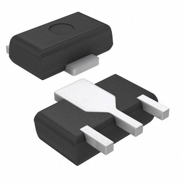
| 供应商器件封装 | 迷你型P3-F1 |
| 其它名称 | 2SD241300LTR |
| 功率-最大值 | 1W |
| 包装 | 带卷 (TR) |
| 安装类型 | 表面贴装 |
| 封装/外壳 | TO-243AA |
| 晶体管类型 | NPN |
| 标准包装 | 1,000 |
| 电压-集射极击穿(最大值) | 400V |
| 电流-集电极(Ic)(最大值) | 100mA |
| 电流-集电极截止(最大值) | - |
| 频率-跃迁 | 40MHz |


- 商务部:美国ITC正式对集成电路等产品启动337调查
- 曝三星4nm工艺存在良率问题 高通将骁龙8 Gen1或转产台积电
- 太阳诱电将投资9.5亿元在常州建新厂生产MLCC 预计2023年完工
- 英特尔发布欧洲新工厂建设计划 深化IDM 2.0 战略
- 台积电先进制程称霸业界 有大客户加持明年业绩稳了
- 达到5530亿美元!SIA预计今年全球半导体销售额将创下新高
- 英特尔拟将自动驾驶子公司Mobileye上市 估值或超500亿美元
- 三星加码芯片和SET,合并消费电子和移动部门,撤换高东真等 CEO
- 三星电子宣布重大人事变动 还合并消费电子和移动部门
- 海关总署:前11个月进口集成电路产品价值2.52万亿元 增长14.8%

PDF Datasheet 数据手册内容提取
This product complies with the RoHS Directive (EU 2002/95/EC). Transistors 2SD2413 Silicon NPN triple diffusion planar type For low-frequency output amplification / Unit: mm e 4.5±0.1 ■ Features 1.6±0.2 1.5±0.1 •High collector-base voltage (Emitter open) V c ••HLaigrghe c coolllelecctotor-re pmoiwtteerr dvioslstiapgaet i(oBna Pse open) VCCEBOO n d +0.254.0–0.20 2.5±0.1 ••LMoiwni cPoolwleecrto try-peem pitatcekr asgateu, raaltlioown ivnoglC tdaogwe nVsCizEia(nsagt) of the equipment e0.41±.05.±008.1 1 20.5±0.038 +0.11.0–0.2 ag3˚e0..4±0.04 and automatic insertion through the tape packing and the magazine u st packing. 3˚ e ■ AbsoluteP aMraamxeitmerum Ratiengs S Tynma b=o 2l 5°CRating Unnit 3.c0t± 0l.i1f5ecycl2.6±0.1 45˚ 0.4 max. i u d Collector-base voltage (Emtitter open) VCBO 4t00 V o 1 : Base Collector-emitter voltange (Base open) VCEO n400 V r Pr 23 :: ECmoliltetcetror Emitter-base voltage (Collector open) VEBO 5 V ou MiniP3-F1 Package Collector currient oIC 100 mA ng fMayrpkeing Symbol: 1S on. ■NPCJSoutteoEMeonal)rclklaeet* gicco:cteoonbP tltr lrorete iieapmacncmrottadpoewp edrPlte e rh cCaarcriuDa ticrdurthrakucirrmnseaueirseenireitstp atsbae cootriatfo ern1sdr .:*7i sC mtoimpcpsc efD oir rTfs otcahi leo= S aTcIPn rTyCo2tseCitmPjlag5l nebo°cufCot ol1e −r ± cd5p m 5io3 p2r21tn°lt o105oiCco a00lr+n nm1u5edo0rdee pl,s maamfCnma°°naoWdiiolCCA lentnnhtotdde eietwdiindoininasassncnccocoenen t ttitgi ynnpuUueeeRddL ttoayynb.ppMopeeiuadnt nlaatsTeoysnpti ic.ncfMoo.rjaxpm/aetin/Unit Collector-base voltage (Emitntecr eo/pen) VCBO IC = 100 µA, IE = 0 owin emic 400 V CEmoliltetcetro-br-aesme ivttoelrt avgoel nt(taCgeoel nl(eBacatsoer ooppeenn)) VVCEBEOO IICE == 150000 µµAA,, IICBs i==t 00follww.s 4500 VV FCoorlwleacrtdo rc-eumrreitntet rMt rsaaaintsufreart iroanti ovoltage VChEF(Esat) VICC =E 5=e0 5 am VsA,e ,I CIvB i= h= t3 t50p m:m//AAw 30 1.5 V Base-emitter saturation voltage VBE(sat) IC =Pl 50 mA, IB = 5 mA 1.5 V Transition frequency * f V = 30 V, I = −20 mA, f = 200 MHz 40 MHz T CB E Collector output capacitance C V = 30 V, I = 0, f = 1 MHz 7 pF ob CB E (Common base, input open circuited) Note)1.Measuring methods are based on JAPANESE INDUSTRIAL STANDARD JIS C 7030 measuring methods for transistors. 2.*:Pulse measurement Publication date: December 2002 SJC00260BED 1
This product complies with the RoHS Directive (EU 2002/95/EC). 2SD2413 P T I V V I C a C CE CE(sat) C 1.2 Copper plate at the collector 120 Ta = 25°C )V 100 IC / IB = 10 )W 1.0 1is. 7m morme tihna tnh i1c kcnme2s sin area, 100 ( E(sat) (Collector power dissipation P C 0000....8642 ()Collector current I mAC 86420000 ncIB =e 1.0000000000 .........975318642m/ mmmmmmmmmAAAAAAAAAA eector-emitter saturation voltage VCd01.110 25°CTa −=2 755°°CC oll e. 0 0a C0.01 g 0 20 40 60 80 100 120 140 160 0 2 4 6 8 10 12 0.1 1 a 10 100 Ambient temperature Ta (°C) Collector-emitter voltage VuCE (V) Collectoer csutrrent IC (mA) n cl y n c e put capacitance()Base-emitter saturation voltage V V (pF)CBE(sat)obase, input open circuited) 0M1.011010.20864111000.1 CaollieVcCt1oDTBMroaE b=ca(ii us−ar2nrtnt5)e ° nCVet nCIt1 Cs0IBa 27CIfT I5E 5(Cn=a m°° =/ =CC1c IA 0 2BMe 5)=/°H Cec1z0D1i0s0coontForward current transfer ratio hiFEn111u852963e00000000n.d1 ipnltCPclaollienlue2ace5dt°1sodCher peF lsc E umamf vriarTnaoie−hislan itl2e= ntttn5I t ot7° dCIfpC15 eC:e0°w o/Cdi nldV/in(limCnasaEsowA gnc=nc ) ww5fcocio Voenwenn 1t. tuti0tgisr0 yn ynepuUpuPreemeeRio()dTransition frequency f MHzdLc T dttoauyyn654321cb.p0000000pt− ope1eliuadft nlEaamtsieot−tesn1rti0 fcicTu. rnrcfenoo .trI j E−IpE1m/ 0 (TV0aemtaC i=BnA / =o2) 53n°0.C V−1000 or outmon b 2 ctm Colle (Co 0 10 100 1000 Collector-base voltage V (V) CB 2 SJC00260BED
Request for your special attention and precautions in using the technical information and semiconductors described in this book (1)(cid:9)If any of the products or technical information described in this book is to be exported or provided to non-residents, the laws and regulations of the exporting country, especially, those with regard to security export control, must be observed. (2)(cid:9)The technical information described in this book is intended only to show the main characteristics and application circuit examples of the products, and no license is granted under any intellectual property right or other right owned by our company or any other company. Therefore, no responsibility is assumed by our company as to the infringement upon any such right owned by any other company which may arise as a result of the use of technical information described in this book. (3)(cid:9)The products described in this book are intended to be used for standard applications or general electronic equipment (such as office / equipment, communications equipment, measuring instruments and household appliances). Consult our sales staff in advance for information on the following applicateions: (cid:150) Special applications (such as for airplanes, aerospace, automobiles, traffic control equipment, combustion equipment, life support systems and safety devices) in which exceptional quality and reliability are required, or if the failure or malfunction of the prod- c ucts may directly jeopardize life or harm the human body. (cid:150) Any applications other than the standard applications intended. d n (4)(cid:9)The products and product specifications described in this book are subject to change without notice for modification and/or im- e provement. At the final stage of your design, purchasing, or use of the products, therefore, ask for the most upe-t.o-date Product Standards in advance to make sure that the latest spaecifications satisfy your requirements. ag u st (5)(cid:9)When designing your equipment, comply with the range of absolute maximum rating and the guarantee ed operating conditions (operating power supply voltage and opernating environment etc.). Especially, please be careful not to yexclceed the range of absolute maximum rating on the transient state, such as power-on, power-onff and mode-switching. Otherwiseec, we will not be liable for any (cid:9) dEevfeecnt wwhheicnh t hmea pyr aordiusec tlsa taerre i nu syeodeu wr eitqhuinip tmhee ngt.uaranteed values, take into the consideration ocf ti nlicfidence of break down and failure i u mode, possible to occur to semiconductor products. Measures on the systems such as redudndant design, arresting the spread of fire or preventing glitch are retcommended in order to prevetnt physical injury, fire, social damoages, for example, by using the products. r n n r P (6)(cid:9)Comply with the instructions for use in order to prevent breakdown and characteruistics change due to external factors (ESD, EOS, o tdhaemrmp-apl rostorfe spisa caknidn gm iesc rheaqnuiicraeld s, tsraetsiss)f ya tt hteho ec otinmdiet ioofn sh, asnudclhin ags, smheoluf nlitfine ga nodnr gtah tfe c eulsatpoysmepdeer t'sim per oscinecsse. fWirsht eonp eunsiinngg tphreo dpuaccktsa ogfoenrs. .which (7)(cid:9)TEMhleics trbioc oIkna dmusatyriD abl eCi noo.,t Lrtedps.rinted coDri srecproondtuicnedu ewdh ietpnhlecalr nuwedhdoe pllsly mamf aonaoiilrl ennptotda erewtdinidinaialsaslyncnc,c ocowenen ti tttitgih ynonupuUute eeRthddL e t topayynrb.pipoopere uadwt nrliatattseneo spntie ricm.ncfisoso.irjonpm/ oaetfi nM/atsushita ce/ win mic n o e ntena sit follww.s ai vi w M se p:// ea htt Pl