ICGOO在线商城 > 分立半导体产品 > 晶体管 - 双极 (BJT) - 单 > 2SD2150T100S
 Datasheet下载
- 型号: 2SD2150T100S
- 制造商: ROHM Semiconductor
- 库位|库存: xxxx|xxxx
- 要求:
| 数量阶梯 | 香港交货 | 国内含税 |
| +xxxx | $xxxx | ¥xxxx |
查看当月历史价格
查看今年历史价格
2SD2150T100S产品简介:
ICGOO电子元器件商城为您提供2SD2150T100S由ROHM Semiconductor设计生产,在icgoo商城现货销售,并且可以通过原厂、代理商等渠道进行代购。 2SD2150T100S价格参考。ROHM Semiconductor2SD2150T100S封装/规格:晶体管 - 双极 (BJT) - 单, 双极 (BJT) 晶体管 NPN 20V 3A 290MHz 500mW 表面贴装 MPT3。您可以下载2SD2150T100S参考资料、Datasheet数据手册功能说明书,资料中有2SD2150T100S 详细功能的应用电路图电压和使用方法及教程。
Rohm Semiconductor的2SD2150T100S是一款双极型晶体管(BJT),属于NPN类型。该型号广泛应用于以下场景:

 1. 功率放大电路
   - 2SD2150T100S具有较高的电流增益和良好的频率特性,适合用于音频功率放大器中,实现信号的高效放大。
   - 常见于家庭音响设备、汽车音响系统或专业音频设备中。

 2. 开关电路
   - 在需要快速开关的应用中,该晶体管可以作为电子开关使用,例如继电器驱动、LED驱动或电机控制。
   - 其低饱和电压特性使其在开关应用中表现出较低的功耗。

 3. 电源管理
   - 可用于线性稳压器或DC-DC转换器中的驱动级,帮助调节输出电压或电流。
   - 在电池管理系统中,可用于监测和控制电池充放电过程。

 4. 工业自动化
   - 在工业控制领域,该晶体管可用于传感器信号放大、PLC(可编程逻辑控制器)输入/输出接口驱动等。
   - 适用于需要高可靠性和稳定性的工业环境。

 5. 通信设备
   - 在通信设备中,2SD2150T100S可用于射频(RF)信号的预放大或驱动级放大。
   - 适用于无线通信模块、对讲机或其他低功率通信设备。

 6. 消费电子产品
   - 该型号常见于家用电器中,如风扇、吸尘器、冰箱等的电机控制电路。
   - 还可用于打印机、扫描仪等办公设备的驱动电路。

 特性总结
2SD2150T100S具备以下优点:
- 高电流增益(hFE),确保良好的放大性能。
- 较高的集电极-发射极击穿电压(Vceo),适应多种电压范围的应用。
- 良好的热稳定性和可靠性,适合长时间运行。

总之,这款晶体管适用于需要中低功率放大和开关功能的各种电子设备和系统中,尤其在音频、工业控制和电源管理领域表现优异。
| 参数 | 数值 |
| 产品目录 | |
| 描述 | TRANS NPN 20V 3A SOT-89两极晶体管 - BJT NPN 20V 3A |
| 产品分类 | 晶体管(BJT) - 单路分离式半导体 |
| 品牌 | ROHM Semiconductor |
| 产品手册 | |
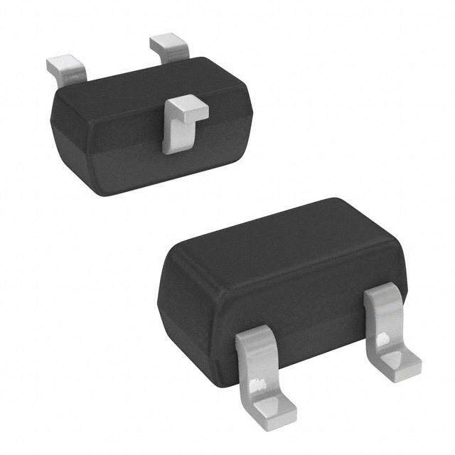
| 产品图片 |
|
| rohs | 符合RoHS无铅 / 符合限制有害物质指令(RoHS)规范要求 |
| 产品系列 | 晶体管,两极晶体管 - BJT,ROHM Semiconductor 2SD2150T100S- |
| 数据手册 | |
| 产品型号 | 2SD2150T100S |
| 不同 Ib、Ic时的 Vce饱和值(最大值) | 500mV @ 100mA,2A |
| 不同 Ic、Vce 时的DC电流增益(hFE)(最小值) | 270 @ 100mA,2V |
| 产品目录绘图 |
|
| 产品目录页面 | |
| 产品种类 | 两极晶体管 - BJT |
| 供应商器件封装 | MPT3 |
| 其它名称 | 2SD2150T100SDKR |
| 功率-最大值 | 500mW |
| 包装 | Digi-Reel® |
| 发射极-基极电压VEBO | 6 V |
| 商标 | ROHM Semiconductor |
| 增益带宽产品fT | 290 MHz |
| 安装类型 | 表面贴装 |
| 安装风格 | SMD/SMT |
| 封装 | Reel |
| 封装/外壳 | TO-243AA |
| 封装/箱体 | SC-62 |
| 工厂包装数量 | 1000 |
| 晶体管极性 | NPN |
| 晶体管类型 | NPN |
| 最大功率耗散 | 0.5 W |
| 最大工作温度 | + 150 C |
| 最大直流电集电极电流 | 3 A |
| 标准包装 | 1 |
| 电压-集射极击穿(最大值) | 20V |
| 电流-集电极(Ic)(最大值) | 3A |
| 电流-集电极截止(最大值) | - |
| 直流电流增益hFE最大值 | 560 |
| 直流集电极/BaseGainhfeMin | 120 |
| 配置 | Single |
| 集电极—发射极最大电压VCEO | 20 V |
| 集电极—基极电压VCBO | 40 V |
| 集电极连续电流 | 3 A |
| 频率-跃迁 | 290MHz |


- 商务部:美国ITC正式对集成电路等产品启动337调查
- 曝三星4nm工艺存在良率问题 高通将骁龙8 Gen1或转产台积电
- 太阳诱电将投资9.5亿元在常州建新厂生产MLCC 预计2023年完工
- 英特尔发布欧洲新工厂建设计划 深化IDM 2.0 战略
- 台积电先进制程称霸业界 有大客户加持明年业绩稳了
- 达到5530亿美元!SIA预计今年全球半导体销售额将创下新高
- 英特尔拟将自动驾驶子公司Mobileye上市 估值或超500亿美元
- 三星加码芯片和SET,合并消费电子和移动部门,撤换高东真等 CEO
- 三星电子宣布重大人事变动 还合并消费电子和移动部门
- 海关总署:前11个月进口集成电路产品价值2.52万亿元 增长14.8%


.jpg)

PDF Datasheet 数据手册内容提取
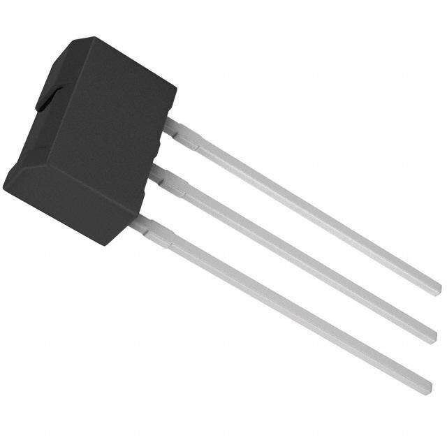
Low Frequency Transistor (20V, 3A) 2SD2150 (cid:122)Features (cid:122)Dimensions(Unit : mm) 1) Low VCE(sat). VCE(sat) = 0.2V(Typ.) 2SD2150 2) (ExIcCe /l lIeBn =t c2uAr r/e 0n.t1 gAa)in characteristics. ±0.50.1 14..65±+−000...121 1.5−+00..12 3) Complements the 2SB1424. ±4.00.3+0.22.5−0.1 (1) (2) (3) 0.4−+00..015 (cid:122)EpSittaruxciatlu prlea nar type ±1.00.210..54±±00..11 0.5±0.1 01..45±±00..11 3.0±0.2 NPN silicon transistor (1) Base ROHM : MPT3 (2) Collector (cid:122)Absolute maximum ratings (Ta=25°C) EIAJ : SC-62 (3) Emitter ∗ Abbreviated symbol: CF Parameter Symbol Limits Unit Collector-base voltage VCBO 40 V ∗ Denotes hFE Collector-emitter voltage VCEO 20 V Emitter-base voltage VEBO 6 V 3 A (DC) Collector current IC 5 A (Pulse) ∗1 0.5 W Collector power dissipation PC 2 W ∗2 Junction temperature Tj 150 °C Storage temperature Tstg −55 to +150 °C ∗1 Single pulse Pw=10ms ∗2 Mounted on a 40×40×0.7mm Ceramic substrate. (cid:122)Electrical characteristics (Ta=25°C) Parameter Symbol Min. Typ. Max. Unit Conditions Collector-base breakdown voltage BVCBO 40 − − V IC=50µA Collector-emitter breakdown voltage BVCEO 20 − − V IC=1mA Emitter-base breakdown voltage BVEBO 6 − − V IE=50µA Collector cutoff current ICBO − − 0.1 µA VCB=30V Emitter cutoff current IEBO − − 0.1 µA VEB=5V Collector-emitter saturation voltage VCE(sat) − 0.2 0.5 V IC/IB=2A/0.1A ∗ DC current transfer ratio hFE 120 − 560 − VCE=2V, IC=0.1A Transition frequency fT − 290 − MHz VCE=2V, IE= −0.5A, f=100MHz Output capacitance Cob − 25 − pF VCE=10V, IE=0A, f=1MHz ∗ Measured using pulse current. www.rohm.com 1/2 2009.11 - Rev.B ○c 2009 ROHM Co., Ltd. All rights reserved.
2SD2150 Data Sheet (cid:122)Packaging specifications and hFE Package Taping Code T100 Basic ordering 1000 Type hFE unit (pieces) 2SD2150 RS hFE values are classified as follows : Item R S hFE 180 to 390 270 to 560 (cid:122)Electrical characteristic curves (A)RRENT : IC 001..025125 Ta= 1−240500°°°CCC VCE=2V (A)RRENT : IC 11..262 21110864mmmmAAAA 12mA10mATa=2865mm°CAA (A)RRENT : IC 345 445500mmmAAA 35m3A0mATa2=5212m055mmA°CAA CU 0.1 CU 4mA CU 10mA OR 0.05 OR 0.8 OR 2 LECT00..0012 LECT 2mA LECT 5mA OL 5m OL 0.4 OL 1 C C C 2m 1m 0 IB=0A 0 IB=0A 0 0.2 0.4 0.6 0.8 1.0 1.2 1.4 0 0.2 0.4 0.6 0.8 1.0 0 1 2 3 4 5 BASE TO EMITTER VOLTAGE : VBE (V) COLLECTOR TO EMITTER VOLTAGE : VCE (V) COLLECTOR TO EMITTER VOLTAGE : VCE (V) Fig.1 Grounded emitter propagation Fig.2 Grounded emitter output Fig.3 Grounded emitter output characteristics characteristics ( ) characteristics ( ) T GAIN : hFE125250000000000000 Ta= 1−240500°°°CCC VCE=2V (V)N VOLTAGE : VCE(sat) 000...21251 Ta=12050°°CC IC/IB=10 (V)N VOLTAGE : VCE(sat) 0.0000...51251 lC/lB=20 Ta=−1 402005°°°CCC REN 100 ATIO50m −40°C ATIO0.02 R R R DC CU 2500 OR SATU1200mm OR SATU0.50m1 T T 10 EC 5m EC 2m 5 OLL 2m OLL 1m 1m2m5m0.010.020.050.10.2 0.5 1 2 5 10 C 1m2m5m10m20m50m0.10.2 0.51 2 5 10 C 1m2m5m0.010.020.050.10.2 0.5 1 2 5 10 COLLECTOR CURRENT : IC (A) COLLECTOR CURRENT : IC (A) COLLECTOR CURRENT : IC (A) Fig.4 DC current gain vs. Fig.5 Collector-emitter Fig.6 Collector-emitter collector current saturation voltage vs. saturation voltage vs. collector current ( ) collector curren ( ) (V)COLLECTOR SATURATION VOLTAGE : VCE(sat) 12500025000...mmmmm212511m2m5m10mTa2=01m−02450500°°°mCCC0.10.2 0.51IC2/IB=55010 TRANSITION FREQUENCY : f(MHz)T 1052121000050052100000−1 −2 −5−10−20 −50−100−20TV0aC−E=5=20250V°−C1000 (pF)COLLECTOR OUTPUT CAPACITANCE : Cob (pF)EMITTER INPUT CAPACITANCE : Cib 11250125000000000000.1 0.2 0.5 1CCoobb2 5 10TfII=ECa==12=00M02AAH5°zC50 COLLECTOR CURRENT : IC (A) EMITTER CURRENT : IE (mA) COELMLIETTCETRO R T OT O B ABSAES E V OVLOTLATGAEG E: V : EVB C(BV ()V) Fig.7 Collector-emitter Fig.8 Gain bandwidth product vs. Fig.9 Collector output capacitance vs. saturation voltage vs. emitter current collector-base voltage collector current ( ) Emitter input capacitance vs. emitter-base voltage www.rohm.com 2/2 2009.11 - Rev.B ○c 2009 ROHM Co., Ltd. All rights reserved.
Notice Notes No copying or reproduction of this document, in part or in whole, is permitted without the consent of ROHM Co.,Ltd. The content specified herein is subject to change for improvement without notice. The content specified herein is for the purpose of introducing ROHM's products (hereinafter "Products"). If you wish to use any such Product, please be sure to refer to the specifications, which can be obtained from ROHM upon request. Examples of application circuits, circuit constants and any other information contained herein illustrate the standard usage and operations of the Products. The peripheral conditions must be taken into account when designing circuits for mass production. Great care was taken in ensuring the accuracy of the information specified in this document. However, should you incur any damage arising from any inaccuracy or misprint of such information, ROHM shall bear no responsibility for such damage. The technical information specified herein is intended only to show the typical functions of and examples of application circuits for the Products. ROHM does not grant you, explicitly or implicitly, any license to use or exercise intellectual property or other rights held by ROHM and other parties. ROHM shall bear no responsibility whatsoever for any dispute arising from the use of such technical information. The Products specified in this document are intended to be used with general-use electronic equipment or devices (such as audio visual equipment, office-automation equipment, commu- nication devices, electronic appliances and amusement devices). The Products specified in this document are not designed to be radiation tolerant. While ROHM always makes efforts to enhance the quality and reliability of its Products, a Product may fail or malfunction for a variety of reasons. Please be sure to implement in your equipment using the Products safety measures to guard against the possibility of physical injury, fire or any other damage caused in the event of the failure of any Product, such as derating, redundancy, fire control and fail-safe designs. ROHM shall bear no responsibility whatsoever for your use of any Product outside of the prescribed scope or not in accordance with the instruction manual. The Products are not designed or manufactured to be used with any equipment, device or system which requires an extremely high level of reliability the failure or malfunction of which may result in a direct threat to human life or create a risk of human injury (such as a medical instrument, transportation equipment, aerospace machinery, nuclear-reactor controller, fuel-controller or other safety device). ROHM shall bear no responsibility in any way for use of any of the Products for the above special purposes. If a Product is intended to be used for any such special purpose, please contact a ROHM sales representative before purchasing. If you intend to export or ship overseas any Product or technology specified herein that may be controlled under the Foreign Exchange and the Foreign Trade Law, you will be required to obtain a license or permit under the Law. Thank you for your accessing to ROHM product informations. More detail product informations and catalogs are available, please contact us. ROHM Customer Support System http://www.rohm.com/contact/ www.rohm.com R0039A © 2009 ROHM Co., Ltd. All rights reserved.