ICGOO在线商城 > 集成电路(IC) > 接口 - 传感器和探测器接口 > XTR101AP
 Datasheet下载
- 型号: XTR101AP
- 制造商: Texas Instruments
- 库位|库存: xxxx|xxxx
- 要求:
| 数量阶梯 | 香港交货 | 国内含税 |
| +xxxx | $xxxx | ¥xxxx |
查看当月历史价格
查看今年历史价格
XTR101AP产品简介:
ICGOO电子元器件商城为您提供XTR101AP由Texas Instruments设计生产,在icgoo商城现货销售,并且可以通过原厂、代理商等渠道进行代购。 XTR101AP价格参考¥52.95-¥63.54。Texas InstrumentsXTR101AP封装/规格:接口 - 传感器和探测器接口, 。您可以下载XTR101AP参考资料、Datasheet数据手册功能说明书,资料中有XTR101AP 详细功能的应用电路图电压和使用方法及教程。
Texas Instruments(德州仪器)的XTR101AP是一款专为传感器接口设计的低功耗、高精度信号调理芯片,广泛应用于工业和过程控制领域。以下是其主要应用场景:

1. 压力传感器信号调理
   XTR101AP常用于桥式压力传感器的信号调理。它可以将微弱的传感器输出信号放大,并转换为标准的4-20mA电流信号,便于远距离传输和工业控制系统兼容。

2. 温度传感器接口
   在温度测量系统中,XTR101AP可用于处理热敏电阻或其他桥式温度传感器的输出信号。通过内置的增益调整和偏移校正功能,确保温度测量的高精度。

3. 液位检测系统
   该芯片可与液位传感器配合使用,将液位变化引起的电信号变化转换为标准电流信号,适用于储罐、管道等液位监控场景。

4. 流量监测
   在流量计应用中,XTR101AP能够处理来自差压流量传感器的信号,将其转换为适合工业控制器读取的标准信号,实现精确的流量监测。

5. 工业自动化设备
   作为传感器接口的核心组件,XTR101AP被广泛应用于各种工业自动化设备中,例如PLC(可编程逻辑控制器)、DCS(分布式控制系统)和其他数据采集系统。

6. 便携式仪器
   由于其低功耗特性,XTR101AP也适用于电池供电的便携式测量仪器,如手持式压力表或温湿度测试仪。

总结来说,XTR101AP以其高集成度、低功耗和高精度的特点,成为工业传感器信号调理的理想选择,尤其适合需要将微弱信号转换为标准4-20mA电流输出的应用场合。
| 参数 | 数值 |
| 产品目录 | 集成电路 (IC)半导体 |
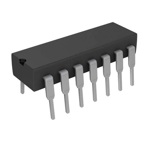
| 描述 | IC TWO-WIRE TRANSMITTER 14 DIP电流灵敏放大器 Prec Lo-Drift 4-20mA 2-Wire Trnsmtr |
| 产品分类 | |
| 品牌 | Texas Instruments |
| 产品手册 | |
| 产品图片 |
|
| rohs | 符合RoHS无铅 / 符合限制有害物质指令(RoHS)规范要求 |
| 产品系列 | 放大器 IC,电流灵敏放大器,Texas Instruments XTR101AP- |
| 数据手册 | |
| 产品型号 | XTR101AP |
| 产品目录页面 | |
| 产品种类 | 电流灵敏放大器 |
| 供应商器件封装 | 14-PDIP |
| 共模抑制比—最小值 | 90 dB |
| 包装 | 管件 |
| 单电源电压 | 11.6 V to 40 V |
| 商标 | Texas Instruments |
| 安装类型 | 通孔 |
| 安装风格 | Through Hole |
| 封装 | Tube |
| 封装/外壳 | 14-DIP(0.300",7.62mm) |
| 封装/箱体 | PDIP-14 |
| 工厂包装数量 | 25 |
| 接口 | 2 线 |
| 最大工作温度 | + 85 C |
| 最小工作温度 | - 40 C |
| 标准包装 | 25 |
| 电流-电源 | 20mA |
| 电源电压-最大 | 40 V |
| 电源电压-最小 | 11.6 V |
| 类型 | 电流发送器 |
| 系列 | XTR101 |
| 输入类型 | 差分 |
| 输入补偿电压 | 0.1 mV |
| 输出类型 | 电压 |
| 通道数量 | 1 Channel |


- 商务部:美国ITC正式对集成电路等产品启动337调查
- 曝三星4nm工艺存在良率问题 高通将骁龙8 Gen1或转产台积电
- 太阳诱电将投资9.5亿元在常州建新厂生产MLCC 预计2023年完工
- 英特尔发布欧洲新工厂建设计划 深化IDM 2.0 战略
- 台积电先进制程称霸业界 有大客户加持明年业绩稳了
- 达到5530亿美元!SIA预计今年全球半导体销售额将创下新高
- 英特尔拟将自动驾驶子公司Mobileye上市 估值或超500亿美元
- 三星加码芯片和SET,合并消费电子和移动部门,撤换高东真等 CEO
- 三星电子宣布重大人事变动 还合并消费电子和移动部门
- 海关总署:前11个月进口集成电路产品价值2.52万亿元 增长14.8%


PDF Datasheet 数据手册内容提取
XTR101 SBOS146A − OCTOBER 1986 − REVISED AUGUST 2004 Precision, Low Drift 4-20mA TWO-WIRE TRANSMITTER FEATURES DESCRIPTION (cid:1) INSTRUMENTATION AMPLIFIER INPUT: The XTR101 is a microcircuit, 4-20mA, two-wire − Low Offset Voltage, 30µV max transmitter containing a high accuracy instrumentation − Low Voltage Drift, 0.75µV/°C max amplifier (IA), a voltage-controlled output current source, − Low Nonlinearity, 0.01% max and dual-matched precision current reference. This (cid:1) combination is ideally suited for remote signal conditioning TRUE TWO-WIRE OPERATION: of a wide variety of transducers such as thermocouples, − Power and Signal on One Wire Pair RTDs, thermistors, and strain gauge bridges. State-of-the- − Current Mode Signal Transmission art design and laser-trimming, wide temperature range − High Noise Immunity operation, and small size make it very suitable for (cid:1) DUAL MATCHED CURRENT SOURCES industrial process control applications. In addition, the optional external transistor allows even higher precision. (cid:1) WIDE SUPPLY RANGE: 11.6V to 40V The two-wire transmitter allows signal and power to be (cid:1) SPECIFICATION RANGE: −40°C to +85°C supplied on a single wire pair by modulating the (cid:1) SMALL DIP-14 PACKAGE, CERAMIC AND power-supply current with the input signal source. The PLASTIC transmitter is immune to voltage drops from long runs and noise from motors, relays, actuators, switches, transformers, and industrial equipment. It can be used by APPLICATIONS OEMs producing transmitter modules or by data acquisition system manufacturers. (cid:1) INDUSTRIAL PROCESS CONTROL: − Pressure Transmitters I REF1 − Temperature Transmitters IREF2 EOxptteiornnaall − Millivolt Transmitters e 3 − 10 11 +VCC Transistor (cid:1) RESISTANCE BRIDGE INPUTS 1 8 (cid:1) THERMOCOUPLE INPUTS 5 (cid:1) RTD INPUTS 12(1) (cid:1) CURRENT SHUNT (mV) INPUTS Span XTR101 B (cid:1) 6 PRECISION DUAL CURRENT SOURCES (cid:1) AUTOMATED MANUFACTURING (cid:1) 4 POWER/PLANT ENERGY SYSTEM e2 + 9 MONITORING 13(1) E 14 7 2 I 1 OUT Optional OffsetNull NOTE:(1)Pins12and13areusedforoptionalBWcontrol. Please be aware that an important notice concerning availability, standard warranty, and use in critical applications of TexasInstruments semiconductor products and disclaimers thereto appears at the end of this data sheet. All trademarks are the property of their respective owners. (cid:1)(cid:2)(cid:3)(cid:4)(cid:5)(cid:6)(cid:7)(cid:8)(cid:3)(cid:9) (cid:4)(cid:10)(cid:7)(cid:10) (cid:11)(cid:12)(cid:13)(cid:14)(cid:15)(cid:16)(cid:17)(cid:18)(cid:11)(cid:14)(cid:12) (cid:11)(cid:19) (cid:20)(cid:21)(cid:15)(cid:15)(cid:22)(cid:12)(cid:18) (cid:17)(cid:19) (cid:14)(cid:13) (cid:23)(cid:21)(cid:24)(cid:25)(cid:11)(cid:20)(cid:17)(cid:18)(cid:11)(cid:14)(cid:12) (cid:26)(cid:17)(cid:18)(cid:22)(cid:27) (cid:1)(cid:15)(cid:14)(cid:26)(cid:21)(cid:20)(cid:18)(cid:19) Copyright 1986-2004, Texas Instruments Incorporated (cid:20)(cid:14)(cid:12)(cid:13)(cid:14)(cid:15)(cid:16) (cid:18)(cid:14) (cid:19)(cid:23)(cid:22)(cid:20)(cid:11)(cid:13)(cid:11)(cid:20)(cid:17)(cid:18)(cid:11)(cid:14)(cid:12)(cid:19) (cid:23)(cid:22)(cid:15) (cid:18)(cid:28)(cid:22) (cid:18)(cid:22)(cid:15)(cid:16)(cid:19) (cid:14)(cid:13) (cid:7)(cid:22)(cid:29)(cid:17)(cid:19) (cid:8)(cid:12)(cid:19)(cid:18)(cid:15)(cid:21)(cid:16)(cid:22)(cid:12)(cid:18)(cid:19) (cid:19)(cid:18)(cid:17)(cid:12)(cid:26)(cid:17)(cid:15)(cid:26) (cid:30)(cid:17)(cid:15)(cid:15)(cid:17)(cid:12)(cid:18)(cid:31)(cid:27) (cid:1)(cid:15)(cid:14)(cid:26)(cid:21)(cid:20)(cid:18)(cid:11)(cid:14)(cid:12) (cid:23)(cid:15)(cid:14)(cid:20)(cid:22)(cid:19)(cid:19)(cid:11)(cid:12)! (cid:26)(cid:14)(cid:22)(cid:19) (cid:12)(cid:14)(cid:18) (cid:12)(cid:22)(cid:20)(cid:22)(cid:19)(cid:19)(cid:17)(cid:15)(cid:11)(cid:25)(cid:31) (cid:11)(cid:12)(cid:20)(cid:25)(cid:21)(cid:26)(cid:22) (cid:18)(cid:22)(cid:19)(cid:18)(cid:11)(cid:12)! (cid:14)(cid:13) (cid:17)(cid:25)(cid:25) (cid:23)(cid:17)(cid:15)(cid:17)(cid:16)(cid:22)(cid:18)(cid:22)(cid:15)(cid:19)(cid:27) www.ti.com
"(cid:7)(cid:2)#$# www.ti.com SBOS146A − OCTOBER 1986 − REVISED AUGUST 2004 ABSOLUTE MAXIMUM RATINGS(1) This integrated circuit can be damaged by ESD. Texas Instruments recommends that all integrated circuits be Power Supply, +VCC . . . . . . . . . . . . . . . . . . . . . . . . . . . . . . . . . 40V handled with appropriate precautions. Failure to observe Input Voltage, e1 or e2 . . . . . . . . . . . . . . . . . . . . ≥ VOUT, ≤ +VCC proper handling and installation procedures can cause damage. Storage Temperature Range, Ceramic. . . . . . . . . −55°C to +165°C ESD damage can range from subtle performance degradation to Plastic. . . . . . . . . . −55°C to +125°C complete device failure. Precision integrated circuits may be more Lead Temperature (soldering, 10s) G, P . . . . . . . . . . . . . . . +300°C susceptible to damage because very small parametric changes could (wave soldering, 3s) U. . . . . . . . . . . . . . +260°C cause the device not to meet its published specifications. Output Short-Circuit Duration . . . . . . . Continuous +VCC to IOUT ORDERING INFORMATION Junction Temperature. . . . . . . . . . . . . . . . . . . . . . . . . . . . . . . +165°C (1)Stresses above these ratings may cause permanent damage. PACKAGE- PACKAGE SPECIFIED PACKAGE Exposure to absolute maximum conditions for extended periods PRODUCT LEAD DESIGNATOR(1) TEMPERATURE MARKING RANGE may degrade device reliability. These are stress ratings only, and functional operation of the device at these or any other conditions CCeerraammiicc JJDD XTR101AG beyond those specified is not supported. DIP-14 XTR101BG XTR101 Plastic −40°C to +85°C N XTR101AP DIP-14 SO-16 DW XTR101AU (1) For the most current package and ordering information, see the Package Option Addendum located at the end of this data sheet. PIN CONFIGURATION Top View DIP Top View SO ZeroAdjust 1 16 ZeroAdjust ZeroAdjust 1 14 ZeroAdjust ZeroAdjust 2 15 Bandwidth ZeroAdjust 2 13 Bandwidth −In 3 14 BControl −In 3 12 BControl SOL−16 +In 4 13 I Surface−Mount REF2 +In 4 DIP 11 I REF2 Span 5 12 I REF1 Span 5 10 I REF1 Span 6 11 E Span 6 9 E Out 7 10 +V CC Out 7 8 +V CC NC 8 9 NC NC = No Connection 2
"(cid:7)(cid:2)#$# www.ti.com SBOS146A − OCTOBER 1986 − REVISED AUGUST 2004 ELECTRICAL CHARACTERISTICS At TA = +25°C, +VCC = 24VDC, and RL = 100Ω with external transistor connected, unless otherwise noted. XTR101AG XTR101BG XTR101AP XTR101AU PARAMETER CONDITIONS MIN TYP MAX MIN TYP MAX MIN TYP MAX MIN TYP MAX UNIT OUTPUT AND LOAD CHARACTERISTICS ∗ ∗ ∗ ∗ ∗ ∗ Current Linear Operating Region 4 20 ∗ ∗ ∗ ∗ ∗ ∗ mA Derated Performance 3.8 22 ∗ ∗ ∗ ∗ mA Current Limit 28 38 31 31 mA Offset Current Error IOS, IO = 4mA ±3.9 ±10 ±2.5 ±6 ±8.5 ±19 ±∗8.5 ±19 µA vs Temperature ∆IOS/∆T ±10.5 ±20 ±8 ±15 ±10.5 ±20 ppm, FS/°C Full-Scale Output Current Full-Scale = 20mA ±20 ±40 ±15 ±30 ±30 ±60 ±30 ±60 µA Error Power-Supply Voltage VCCCo,m Ppinlias n7c ean(1d) 8, +11.6 ±40 ∗ ∗ ∗ ∗ ∗ ∗ VDC Load Resistance At VCC = +24V, 600 ∗ ∗ ∗ Ω IO = 20mA At VCC = +40V, 1400 ∗ ∗ ∗ Ω IO = 20mA SPAN Output Current Equation RS in Ω, e1 and e2 in V IO(cid:1)4mA(cid:2)(cid:3)0.016amps(cid:4)volt(cid:2)(cid:5)40(cid:4)RS(cid:6)(cid:7)(cid:5)e2(cid:8)e1(cid:6) (cid:3) (cid:5) (cid:6)(cid:7) Span Equation RS in Ω S∗(cid:1) 0.016∗amps(cid:4)volt(cid:2) 40(cid:4)∗RS ∗ ∗ ∗ A/V vs Temperature Excluding TCR of RS ±30 ±100 ∗ ∗ ∗ ∗ ∗ ∗ ∗ ∗ ∗ ppm/°C Untrimmed Error(2) εSPAN −5 −2.5 0 ∗ ∗ ∗ % Nonlinearity εNONLINEARITY 0.01 ∗ ∗ ∗ % Hysteresis 0 ∗ ∗ ∗ % Dead Band 0 % INPUT CHARACTERISTICS ∗ ∗ ∗ Impedance: Differential 0.4 3 ∗ ∗ ∗ GΩpF Common-Mode 10 3 ∗ ∗ ∗ ∗ ∗ ∗ GΩ pF Voltage Range, Full-Scale ∆e = (e2 − e1)(3) 0 1 ∗ ∗ V Offset Voltage VOS ±30 ±60 ±20 ±30 ∗ ±1∗00 ∗ ±1∗00 µV vs Temperature ∆VOS/∆T ±0.75 ±1.5 ∗ ±0∗.35 ±0.75 ∗ ∗ µV/°C Power-Supply Rejection ∆VCC/PSRR = VOS Error 110 125 ∗ ∗ 1∗22 ∗ 1∗22 ∗ dB Bias Current IB 60 150 ∗ ∗ ∗ ∗ ∗ ∗ nA vs Temperature ∆IB/∆T 0.30 1 ∗ ∗ ∗ ∗ ∗ nA/°C Offset Current IOSI 10 ±30 ∗ ±∗20 ∗ ∗ ∗ ∗ nA vs Temperature ∆IOSI/∆T 0.1 0.3 nA/°C Common-Mode ∗ ∗ ∗ ∗ ∗ ∗ Rejection(4) DC 90 100 ∗ ∗ ∗ ∗ ∗ ∗ dB Common-Mode Range e1 and e2 with Respect to Pin 7 4 6 V CURRENT SOURCES ∗ ∗ ∗ Magnitude 1 mA Accuracy VCC = 24V, ±0.1 ±0.02 VPRIN2 8= −5 kVΩP,I Nse 1e0 F, i1g1u r=e 159V, ±0.06 7 5 ±0.075 ±∗0.2 ±0∗.37 ±∗0.2 ±0∗.37 % vs Temperature ±50 ±80 ±∗30 ±50 ∗ ∗ ppm/°C vs VCC ±3 ∗ ∗ ∗ ppm/V vs Time ±8 ppm/month Compliance Voltage Ratio With Respect to ∗ ∗ ∗ ∗ ∗ ∗ Match Pin 7 Tracking 0 VCC − 3.5 V ±0.01 ±0.0 ±0.00 Accuracy (1 − IREF1/IREF2) × 100% 4 6 9 ±0.04 ±0.031 ±0∗.088 ±0.031 ±0∗.088 % vs Temperature ±15 ∗ 10 ∗ ∗ ppm/°C vs VCC ±10 ∗ ∗ ∗ ppm/V vs Time ±1 ∗ ∗ ∗ ∗ ppm/month Output Impedance 10 20 15 15 MΩ TEMPERATURE RANGE ∗ ∗ ∗ ∗ ∗ ∗ Specification −40 +85 ∗ ∗ °C Operating −55 +125 ∗ ∗ −40 +85 −40 +85 °C Storage −55 +165 −55 +125 −55 +125 °C ∗ Same as XTR101AG. (1) See the Typical Characteristics. (2) Span error shown is untrimmed and may be adjusted to zero. (3) e1 and e2 are signals on the −In and +In terminals with respect to the output, pin 7. While the maximum permissible ∆e is 1V, it is primarily intended for much lower signal levels, for instance, 10mV or 50mV full-scale for the XTR101A and XTR101B grades, respectively. 2mV FS is also possible with the B grade, but accuracy will degrade due to possible errors in the low value span resistance and very high amplification of offset, drift, and noise. (4) Offset voltage is trimmed with the application of a 5V common-mode voltage. Thus, the associated common-mode error is removed. See the Application Information section. 3
"(cid:7)(cid:2)#$# www.ti.com SBOS146A − OCTOBER 1986 − REVISED AUGUST 2004 TYPICAL CHARACTERISTICS At TA = +25°C and VCC = 24VDC, unless otherwise noted. SPANvsFREQUENCY STEPRESPONSE 80 25 C =0 )Ω RS=25Ω C RS=∞ m 20 ance(20Log 6400 RRRSS===214k00Ω00ΩΩ Current(mA) 15 RS=25Ω conduct 20 RSS=∞ Output 10 s 5 n a Tr 0 0 100 1k 10k 100k 1M 0 200 400 600 800 1000 Frequency(Hz) Time(µs) FULL−SCALEINPUTVOLTAGEvsR S R (kΩ) S COMMON−MODEREJECTIONvsFREQUENCY 0 2 4 6 8 120 0.08 0.8 100 (V) 0.06 0to800mVand 0.6 (V) 80 ale 0to8kΩscale ale B) c c d −S 0.04 0.4 −S R( 60 ull ull M F F C eIN eIN 40 ∆ 0.02 0.2 ∆ 20 0to80mV(low−levelsignals) and0to400Ωscale 0 0 0 0 100 200 300 400 0.1 1 10 100 1k 10k 100k R (Ω) Frequency(Hz) S POWER−SUPPLYREJECTIONvsFREQUENCY BANDWIDTHvsPHASECOMPENSATION 140 100k dB) 120 10k R =∞ ( S Rejection 10800 dth(Hz) 1010k RS=100Ω RS=400Ω Supply 60 Bandwi 10 RS=25Ω er− 40 w Po 20 1 0 0.1 0.1 10 100 1k 10k 100k 1M 10M 1 10 100 1k 10k 100k 1M Frequency(Hz) BandwidthControl,C (pF) C 4
"(cid:7)(cid:2)#$# www.ti.com SBOS146A − OCTOBER 1986 − REVISED AUGUST 2004 TYPICAL CHARACTERISTICS (continued) At TA = +25°C, VDD = +3.3V, and VIO = +3.3V, unless otherwise noted. INPUTVOLTAGENOISEDENSITYvsFREQUENCY INPUTCURRENTNOISEDENSITYvsFREQUENCY 60 6 z) 50 z) 5 H H V/ A/ n 40 p 4 ( ( oltage 30 urrent 3 V C e e s s oi 20 oi 2 N N ut ut p p n 10 n 1 I I 0 0 1 10 100 1k 10k 100k 1 10 100 1k 10k 100k Frequency(Hz) Frequency(Hz) OUTPUTCURRENTNOISEDENSITYvsFREQUENCY 6 z) 5 H A/ (n 4 nt e Curr 3 e s Noi 2 ut p ut 1 O 0 1 10 100 1k 10k 100k Frequency(Hz) 5
"(cid:7)(cid:2)#$# www.ti.com SBOS146A − OCTOBER 1986 − REVISED AUGUST 2004 THEORY OF OPERATION Examination of the transfer function shows that I has a O lower range-limit of 4mA when e = e − e = 0V. This 4mA IN 2 1 A simplified schematic of the XTR101 is shown in Figure 1. is composed of 2mA quiescent current exiting pin 7 plus Basically, the amplifiers A1 and A2 act as a single 2mA from the current sources. The upper range limit of IO power-supply instrumentation amplifier controlling a is set to 20mA by the proper selection of R based on the S current source, A3 and Q1. Operation is determined by an upper range limit of eIN. Specifically, RS is chosen for a internal feedback loop. e1 applied to pin 3 will also appear 16mA output current span for the given full-scale input at pin 5, and similarly, e2 will appear at pin 6. Therefore, the voltage span. (cid:5) (cid:6) current in R (the span setting resistor) will be I =(e −e )/RS =e /R . This current combines with the Forexample, 0.016amps(cid:2)40 (cid:5)e full−scale(cid:6)(cid:1)16mA. S 2 1 S IN S volt R IN current I to form I . The circuit is configured such that I S 3 1 2 is 19 times I1. From this point, the derivation of the transfer Note that since IO is unipolar, e2 must be kept larger than function is straightforward but lengthy. The result is shown e1 (that is, e2 ≥ e1 or eIN ≥ 0). Also note that in order not to in Figure 1. exceed the output upper range limit of 20mA, eIN must be kept less than 1V when R = ∞ and proportionately less as S R is reduced. S − eIN + R S (e) (e) 1 I 2 5 S 6 I I 3 4 R R 3 4 1.25kΩ 1.25kΩ +V +V CC CC +V CC D (e1) IB1 A1 A2 8 1 −In 3 e IN I B2 V +In PS (e)4 100µA 2 I 7 O Q + 1 +VCC +VCC 2mA eL− RL I1 R1 A3 1kΩ R 52.6Ω 2 I 2 I O Voltage−Controlled CurrentSource 10 11 I I 2.5kΩ REF1 REF2 (cid:5) (cid:6) I (cid:1)4mA(cid:2) 0.016amps(cid:2)40 e e (cid:1)e (cid:8)e O volt R IN, IN 2 1 S Figure 1. Simplified Schematic of the XTR101 6
"(cid:7)(cid:2)#$# www.ti.com SBOS146A − OCTOBER 1986 − REVISED AUGUST 2004 INSTALLATION AND OPTIONAL EXTERNAL TRANSISTOR OPERATING INSTRUCTIONS The optional external transistor, when used, is connected in parallel with the XTR101 internal transistor. The purpose BASIC CONNECTION is to increase accuracy by reducing heat change inside the See Figure 1 for the basic connection of the XTR101. A XTR101 package as the output current spans from difference voltage applied between input pins 3 and 4 will 4-20mA. Under normal operating conditions, the internal cause a current of 4-20mA to circulate in the two-wire transistor is never completely turned off, as shown in output loop (through R , V , and D ). For applications L PS 1 Figure 2. This maintains frequency stability with varying requiring moderate accuracy, the XTR101 operates very external transistor characteristics and wiring capacitance. cost-effectively with just its internal drive transistor. For The actual current sharing between internal and external more demanding applications (high accuracy in high gain), transistors is dependent on two factors: an external NPN transistor can be added in parallel with 1. relative geometry of emitter areas, and the internal one. This keeps the heat out of the XTR101 package and minimizes thermal feedback to the input 2. relative package dissipation (case size and thermal stage. Also, in such applications where the e full-scale conductivity). IN is small (< 50mV) and RSPAN is small (< 150Ω), caution For best results, the external device should have a larger should be taken to consider errors from the external span base-emitter area and smaller package. It will, upon circuit plus high amplification of offset drift and noise. turn-on, take about [0.95(I − 3.3mA)]mA. However, it will O heat faster and take a greater share after a few seconds. 4mA 20mA 16mA +V CC 8 750Ω(2) 12V,200mW 3.5mA 0.5mA B 12 QEXT 23.6V,377mW XTR101 Q 18mW 2N2222(1) INT OtherSuitableTypes Type Package 9 VPS 210Ω 3.47V,60mW E 2N4922 TO−225 40V 1.5mA TIP29B TO−220 TIP31B TO−220 Quiescent 52.6Ω 0.95V,17mW I 7 OUT 11 Short−Circuit R 10 Worst−Case 25L0Ω 1mA 1mA 18mA 20mA 2mA NOTES:(1)An external transistor is used in the manufacturing test circuit for testing electrical specifications. (2)Thisresistorisrequiredforthe2N2222withV >24Vtolimitpowerdissipation. PS Figure 2. Power Calculation of the XTR101 with an External Transistor 7
"(cid:7)(cid:2)#$# www.ti.com SBOS146A − OCTOBER 1986 − REVISED AUGUST 2004 Although any NPN of suitable power rating will operate MAJOR POINTS TO CONSIDER WHEN with the XTR101, two readily available transistors are USING THE XTR101 recommended: 1. The leads to R should be kept as short as possible S to reduce noise pick-up and parasitic resistance. 1. 2N2222 in the TO-18 package. For power-supply voltages above 24V, a 750Ω, 1/2W resistor should be 2. +VCC should be bypassed with a 0.01µF capacitor as close to the unit as possible (pin 8 to pin 7). connected in series with the collector. This will limit the power dissipation to 377mW under the worst-case 3. Always keep the input voltages within their range of conditions; see Figure 2. Thus, the 2N2222 will safely linear operation, +4V to +6V (e and e measured with 1 2 operate below its 400mW rating at the upper respect to pin 7). temperature of +85°C. Heat sinking the 2N2222 will 4. The maximum input signal level (e ) is 1V with INFS result in greatly reduced accuracy improvement and R = ∞ and proportionally less as R decreases. S S is not recommended. 5. Always return the current references (pins 10 and 11) 2. TIP29B in the TO-220 package. This transistor will to the output (pin 7) through an appropriate resistor. If operate over the specified temperature and output the references are not used for biasing or excitation, voltage range without a series collector resistor. Heat connect them together to pin 7. Each reference must sinking the TIP29B will result in slightly less accuracy have between 0V and +(VCC − 4V) with respect to improvement. It can be done, however, when pin7. mechanical constraints require it. 6. Always choose R (including line resistance) so that L the voltage between pins 7 and 8 (+V ) remains CC within the 11.6V to 40V range as the output changes ACCURACY WITH AND WITHOUT AN between the 4-20mA range (as shown in Figure 4). EXTERNAL TRANSISTOR 7. It is recommended that a reverse polarity protection The XTR101 has been tested in a circuit using an external diode (D in Figure 1) be used. This will prevent transistor. The relative difference in accuracy with and 1 damage to the XTR101 caused by a momentary (such without an external transistor is shown in Figure 3. Notice as a transient) or long-term application of the wrong that a dramatic improvement in offset voltage change with polarity of voltage between pins 7 and 8. supply voltage is evident for any value of load resistor. 8. Consider PC board layout which minimizes parasitic capacitance, especially in high gain. 30 60 Span=∆I =16mA O C) 1500 25 50(cid:2) ( WithoutExternalTransistor e ur 1250 ∆µV(V)OS 211050 RL=100ΩRL=600Ω RL=1kΩ 432000∆HeatingTemperat ΩResistance,R()L 1075050000 RLmax = VPS2−0m11A.6VOperating 5 WithRELx=te1rn0a0lΩTransistRorL=600Ω RL=1kΩ 10Self− Load 250 Region 0 0 10 20 30 40 0 V (V) CC 0 10 20 30 40 50 60 Power−SupplyVoltage,V (V) PS Figure 3. Thermal Feedback Due to Change in Output Current Figure 4. Power-Supply Operating Range 8
"(cid:7)(cid:2)#$# www.ti.com SBOS146A − OCTOBER 1986 − REVISED AUGUST 2004 SELECTING THE R S R(eSPAN) iws ilcl hreossuelnt ins oth teh adte sai regdiv efunl l-fsuclla-slec aoluet pinupt ustp asnp aonf e1 3 −11 10 8 D1 INFS ∆I : OFS (cid:3)(cid:5) (cid:6) (cid:5) (cid:6)(cid:7) − R5 4−20mA 0.016amps (cid:2) 40 (cid:1)e (cid:1)(cid:1)I (cid:1)16mA. 2mA e ASdj. XTR101 volt R IN O IN 0.01µF S + 6 + 24V + e L Solving for RS: e 7 − RL − 2 4 + 2 14 RS(cid:1)(cid:1)IO(cid:4)(cid:1)eIN(cid:8)400.016avmoplts (1) + e’2 0.01µ1F1MΩ OIfOfset Adjust (cid:5) (cid:6) For example, if ∆eINFS = 100mV for ∆IOFS = 16mA, 2.R52kΩ IO(cid:1)4mA(cid:2) 0.016avmoplts(cid:2)R40 eIN S RS(cid:1)(cid:5)16mA(cid:4)1004m0V(cid:6)(cid:8)0.016(cid:1)0.16(cid:8)400.016 2+m5VA eIN(cid:1)e2 (cid:1) 40 (cid:1)278(cid:2) Figure 5. Basic Connection for Floating Voltage 0.144 Source See the Typical Characteristics for a plot of R vs ∆e . S INFS Nlimoitte, tehat imn uosrdt ebr en olet stos etxhcaene d1 Vth ew 2h0emn AR up p=e r∞ r anagned e1 3 − 11 10 D1 IN S 1mA 1mA 8 proportionately smaller as R decreases. S 5 BIASING THE INPUTS + Because the XTR operates from a single supply, both e1 e−IN RS6 XTR101 0.01µF + 24V + and e must be biased approximately 5V above the e 2 L − R − voltage at pin 7 to assure linear response. This is easily L done by using one or both current sources and an external e2 4 + 214 7 resistor, R2. Figure 5 shows the simplest case—a floating + 1100kΩ Offset voltage source e(cid:9)2. The 2mA from the current sources e2 RT 1MΩ Adjust flows through the 2.5kΩ value of R2 and both e1 and e2 are − 2.R52kΩ raised by the required 5V with respect to pin 7. For linear operation the constraint is: 2mA (cid:5) (cid:6) Alternatecircuitry +5V IO(cid:1)4mA(cid:2) 0.016avmoplts(cid:2)R40 eIN +4V ≤ e ≤ +6V showninFigure8. S 1 eIN(cid:1)e(cid:9)2(cid:1)1mA(cid:10)RT +4V ≤ e ≤ +6V 0.01µF 2 Figure 6. Basic Connection for Resistive Source The offset adjustment is used to remove the offset voltage of the input amplifier. When the input differential voltage CMV AND CMR (e ) equals zero, adjust for 4mA output. IN The XTR101 is designed to operate with a nominal 5V Figure 6 shows a similar connection for a resistive common-mode voltage at the input and will function transducer. The transducer could be excited either by one properly with either input operating over the range of 4V to (as shown) or both current sources. Also, the offset 6V with respect to pin 7. The error caused by the 5V CMV adjustment has higher resolution compared to Figure 5. is already included in the accuracy specifications. If the inputs are biased at some other CMV, then an input offset error term is (CMV − 5)/CMRR, where CMR is in dB, and CMRR is in V/V. 9
"(cid:7)(cid:2)#$# www.ti.com SBOS146A − OCTOBER 1986 − REVISED AUGUST 2004 SIGNAL SUPPRESSION AND ELEVATION In some applications, it is desired to have suppressed zero 1mA 1mA − 1mA 1mA − range (input signal elevation) or elevated zero range (input e e IN IN signal suppression). This is easily accomplished with the + + XTR101 by using the current sources to create the suppression/elevation voltage. The basic concept is + + shown in Figure 7 and Figure 8(a). In this example, the V4 R4 + e’2 RT − sensor voltage is derived from RT (a thermistor, RTD, or − e’2 RT + other variable resistance element) and excited by one of − V R 4 4 the 1mA current sources. The other current source is used − to create the elevated zero range voltage. Figure 8(b), (c), 2mA 2mA and (d) show some of the possible circuit variations. These e =(e’ −V) e =(e’ +V) IN 2 4 IN 2 4 circuits have the desirable feature of noninteractive span V =1mA×R V =1mA×R 4 4 4 4 and suppression/elevation adjustments. e’2=1mA×RT e’2=1mA×RT (a)ElevatedZeroRange (b)SuppressedZeroRange Note: It is not recommended to use the optional offset voltage null (pins 1, 2, and 14) for elevation/suppression. This trim capability is used only to null the amplifier’s input offset voltage. In many applications the already low offset 2mA − 2mA − e e voltage (typically 20µV) will not need to be nulled at all. IN+ IN+ Adjusting the offset voltage to non-zero values will disturb − e’2+ the voltage drift by ±0.3µV/°C per 100µV or induced offset. + V R + 4 4 + − e’2 V4 R4 − − 20 SpanAdjust 2mA 2mA e =(e’ −V) e =(e’ +V) IN 2 4 IN 2 4 V =2mA×R V =2mA×R 15 4 4 4 4 (c)ElevatedZeroRange (d)SuppressedZeroRange A) Figure 8. Elevation and Suppression Circuits m 10 ( O I Suppressed Elevated Zero APPLICATION INFORMATION Zero 5 Range Range The small size, low offset voltage and drift, excellent linearity, and internal precision current sources make the 0 XTR101 ideal for a variety of two-wire transmitter −0+ applications. It can be used by OEMs producing different e (V) IN types of transducer transmitter modules and by data acquisition systems manufacturers who gather transducer data. Current-mode transmission greatly reduces noise Figure 7. Elevation and Suppression Graph interference. The two-wire nature of the device allows economical signal conditioning at the transducer. Thus the XTR101 is, in general, very suitable for individualized and special-purpose applications. 10
"(cid:7)(cid:2)#$# www.ti.com SBOS146A − OCTOBER 1986 − REVISED AUGUST 2004 EXAMPLE 1 An RTD transducer is shown in Figure 9. e1 11 D1 Given a process with temperature limits of +25°C and 3 − 10 8 +150°C, configure the XTR101 to measure the temperature with a platinum RTD which produces 100Ω at 5 − 0°C and 200Ω at +266°C (obtained from standard RTD R tables). Transmit 4mA for +25°C and 20mA for +150°C. e+IN S XTR101 0.01µF 6 + 24V + e COMPUTING RS: L− R − Texhcei tseedn wsiittihvi tay o1fm thAe cRuTrrDe nist ∆soRu/∆rcTe =f o1r0 a0 Ω2/52°6C6 °tCo . 1W50h°eCn V4+− R4 e2 4 + 7 L + r1amnAge× (1(0a0 Ω1/22656°C°C ) ×s p1a2n5)°,C =th 4e7 mVsp =a n∆ e o.f eIN is e’2− RT IN R 2 FromEquation1, R (cid:1) 40 S (cid:1)I (cid:4)(cid:1)e (cid:8)0.016amps O IN volt R (cid:1) 40 (cid:1) 40 (cid:1)123.3(cid:2) 0.01µF S 16mA(cid:4)47mV(cid:8)0.016A(cid:4)V 0.3244 Figure 9. Circuit for Example 1 Span adjustment (calibration) is accomplished by trimming R . EXAMPLE 2 S A thermocouple transducer is shown in Figure 10. COMPUTING R : 4 Given a process with temperature (T ) limits of 0°C and At (cid:2)25oC,e(cid:9) (cid:1)1mA(R (cid:2)(cid:1)R ) 1 2 (cid:3) T T (cid:7) +1000°C, configure the XTR101 to measure the (cid:1)1mA 100(cid:2)(cid:2) 100(cid:2) (cid:10)25oC temperature with a type J thermocouple that produces a 266oC 58mV change for 1000°C change. Use a semiconductor (cid:1)1mA(109.4(cid:2))(cid:1)109.4mV diode for cold junction compensation to make the measurement relative to 0°C. This is accomplished by In order to make the lower range limit of 25°C correspond supplying a compensating voltage (VR6) equal to that to the output lower range limit of 4mA, the input circuitry normally produced by the thermocouple with its cold shown in Figure 9 is used. junction (T2) at ambient. At a typical ambient of +25°C, this e , the XTR101 differential input, is made 0 at 25°C or: is 1.28mV (obtained from standard thermocouple tables IN with reference junction of 0°C). Transmit 4mA for T = 0°C 1 e(cid:9)2 25oC(cid:8)V4 and 20mA for T1 = +1000°C. Note: eIN = e2 − e1 indicates thus, V (cid:1)e(cid:9) (cid:1)109.4mV that T1 is relative to T2. 4 2 25oC R (cid:1) V4 (cid:1)109.4mV(cid:1)109.4(cid:2) 4 1mA 1mA 1mA 1mA R COMPUTING R AND CHECKING CMV: 5 2 2kΩ 11 At (cid:2)25oC,e(cid:9) (cid:1)109.4mV 3 − 10 2 D 8 At (cid:2)150oC,e(cid:9) (cid:1)1mA(R (cid:2)(cid:1)R ) (cid:3) 2 T (cid:7)T R6 (cid:1)1mA 100(cid:2)(cid:2)216060o(cid:2)C(cid:10)150oC e+−1 51ΩeIN XTR101 (cid:1)156.4mV Thermocouple T TC Since both e(cid:9)2 and V4 are small relative to the desired 5V 4 + 7 common-mode voltage, they may be ignored in computing + 0.01µF R as long as the CMV is met. VTC +V4− e−2 2 R (cid:1) 5V (cid:1)2.5k(cid:2) TemperatureT1 R4 2.5kΩ 2 2mA (cid:11) TemperatureT2=TD e min(cid:1)5V(cid:2)0.1094V 2 e max(cid:1)5V(cid:2)0.1564V The 4V to 6V CMV Figure 10. Thermocouple Input Circuit with Two 2 requirement is met. e (cid:1)5V(cid:2)0.1094V Temperature Regions and Diode (D) Cold 1 Junction Compensation 11
"(cid:7)(cid:2)#$# www.ti.com SBOS146A − OCTOBER 1986 − REVISED AUGUST 2004 ESTABLISHING R : R is chosen as 2kΩ to be much larger than the resistance S 5 of the diode. Solving for R yields 51Ω. The input full-scale span is 58mV (∆e = 58mV). 6 INFS R is found from Equation 1. S R (cid:1) 40 S (cid:1)I (cid:4)(cid:1)e (cid:8)0.016amps 1mA O IN volt (cid:1) 40 (cid:1) 40 (cid:1)153.9(cid:2) 16mA(cid:4)58mV(cid:8)0.016A(cid:4)V 0.2599 + R V 5 5 − SELECTING R : + 4 V D D R4 is chosen to make the output 4mA at TTC = 0°C − + (V = −1.28mV) and T = +25°C (V = 0.6V); see R V TC D D 6 6 Figure 10. − V will be −1.28mV when T = 0°C and the reference TC TC junction is at +25°C. e must be computed for the condition 1 of T = +25°C to make e = 0V. D IN V (cid:1)600mV D25oC (cid:5) (cid:6) Figure 11. Cold Junction Compensation Circuit e (cid:1)600mV 51 (cid:1)14.9mV 125oC 2051 THERMOCOUPLE BURN-OUT INDICATION e (cid:1)e (cid:8)e (cid:1)V (cid:2)V (cid:8)e IN 2 1 TC 4 1 In process control applications it is desirable to detect when a thermocouple has burned out. This is typically With e = 0 and V = −1.28mV, IN TC done by forcing the two-wire transmitter current to either V (cid:1)e (cid:2)e (cid:8)V 4 1 IN TC limit when the thermocouple impedance goes very high. (cid:1)14.9mV(cid:2)0V(cid:8)((cid:8)1.28mV) The circuits of Figure 16 and Figure 17 inherently have 1mA(R )(cid:1)16.18mV downscale indication. When the impedance of the 4 R (cid:1)16.18(cid:2) thermocouple gets very large (open) the bias current 4 flowing into the + input (large impedance) will cause I to O go to its lower range limit value (about 3.8mA). If upscale COLD JUNCTION COMPENSATION: indication is desired, the circuit of Figure 18 should be A temperature reference circuit is shown in Figure 11. used. When T opens, the output will go to its upper range C limit value (about 25mA or higher). The diode voltage has the form: V (cid:1)KT ln IDIODE OPTIONAL INPUT OFFSET VOLTAGE TRIM D q I SAT The XTR101 has provisions for nulling the input offset Typically at T2 = +25°C, VD = 0.6V and ∆VD/∆T = −2mV/°C. voltage associated with the input amplifiers. In many R5 and R6 form a voltage divider for the diode voltage VD. applications the already low offset voltages (30µV max for The divider values are selected so that the gradient the B grade and 60µV max for the A grade) will not need ∆VD/∆T equals the gradient of the thermocouple at the to be nulled at all. The null adjustment can be done with a reference temperature. At +25°C this is approximately potentiometer at pins 1, 2, and 14; see Figure 5 and 52µV/°C (obtained from a standard thermocouple table); Figure 6. Either of these two circuits may be used. therefore, NOTE:It is not recommended to use this input offset (cid:5) (cid:6) voltage nulling capability for elevation or suppression. See (cid:1)T (cid:1)V R C(cid:1) D 6 the Signal Suppression and Elevation section for the (cid:1)T (cid:1)T R (cid:2)R proper techniques. 5(cid:5) 6 (cid:6) 52(cid:3)V 2000(cid:3)V R (cid:1) 6 °C °C R (cid:2)R 5 6 (2) 12
"(cid:7)(cid:2)#$# www.ti.com SBOS146A − OCTOBER 1986 − REVISED AUGUST 2004 OPTIONAL BANDWIDTH CONTROL 0.0047µF Low-pass filtering is recommended where possible and 1mA can be done by either one of two techniques; see R3(1) 3 − 11 Figure 12. C connected to pins 3 and 4 will reduce the 2 1mA bandwidth with a cutoff frequency given by: f (cid:1) 15.9 C2 XTR101 CO (R (cid:2)R (cid:2)R (cid:2)R )(C (cid:2)3pF) 1 2 3 4 2 R 1 This method has the disadvantage of having fCO vary with R(1) R1, R2, R3, R4, and it may require large values of R3 and 4 4 + 13 R4. The other method, using C1, will use smaller values of R 12 C1 capacitance and is not a function of the input resistors. It 2 is, however, more subject to nonlinear distortion caused by slew rate limiting. This is normally not a problem with the NOTE:(1)R andR shouldbeequalifused. 3 4 slow signals associated with most process control transducers. The relationship between C1 and fCO is InternallyeNOISERTI= e2INPUTSTAGE+ e2OUTPUTSTAGE 2 shown in the Typical Characteristics. Gain Figure 12. Optional Filtering APPLICATION CIRCUITS Voltage Reference MC1403A + V =2.5V R − 100pF XTR101 V+ I O OPA27 (4−20mA) V− R R 1 2 125Ω 500Ω I(cid:9)(0−20mA) O (cid:5) (cid:6) R V NOTE: IO(cid:9)(cid:1) 1(cid:2)R1 IO(cid:8)RR(cid:1)1.25 IO(cid:8)5mA 2 2 Otherconversionsarereadilyachievableby changingthereferenceandratioofR toR. 1 2 Figure 13. 0-20mA Output Converter 13
"(cid:7)(cid:2)#$# www.ti.com SBOS146A − OCTOBER 1986 − REVISED AUGUST 2004 2mA 0.9852mA 1.0147mA 1.8kΩ − LM129 R R 6.9V Voltage 300Ω R XTR101 S Ref R R + 0.01µF 4.7kΩ Figure 14. Bridge Input, Voltage Excitation 2mA 1mA 1mA Thiscircuithasdownscale R R 2kΩ burn−outindication. − 300Ω − TypeJ − + R R 51Ω R 20Ω S XTR101 R XTR101 S J + Zero + 2.2kΩ Adjust 2.5kΩ Figure 15. Bridge Input, Current Excitiation Figure 17. Thermocouple Input with Diode Cold Junction Compensation 1mA 1mA 1mA Thiscircuithasdownscale 1mA Thiscircuithasupscale − burn−outindication. + − − burn−out indication. TypeJ − + 15Ω 1R0T0DΩ 2Z0eΩro RS XTR101 15Ω 1R0T0DΩ 20Ω Zero RS XTR101 Adjust Adjust + + 2.5kΩ 2.5kΩ Figure 16. Thermocouple Input with RTD Cold Figure 18. Thermocouple Input with RTD Cold Junction Compensation Junction Compensation 14
"(cid:7)(cid:2)#$# www.ti.com SBOS146A − OCTOBER 1986 − REVISED AUGUST 2004 11 I I 1 2 10 +VCC 8 − +VCC 3 OPA21 V REF Out R R 1 2 15V 0.01µF XTR101 4 + 7 2.5kΩ V =ImAR REF 2 Figure 19. Dual Precision Current Sources Operated from One Supply Isolation Barrier +15V +V P+ − 2 1kΩ C 8 −V2 722 V+ 1µF 2 E 1µF C +V −V V− 4−20mA 1 1 1 + ∆e XTR101 30V +15V IN − 7 1MΩ + + 10 12 1MΩ −15V 15 7 2 250Ω ISO100 4 3 V (1) 9 8 +1VOUtoT+5V I REF2 17 − 16 18 NOTE:(1)Canbeshiftedandamplified usingISO100currentsources. I REF1 Figure 20. Isolated Two-Wire Current Loop 15
"(cid:7)(cid:2)#$# www.ti.com SBOS146A − OCTOBER 1986 − REVISED AUGUST 2004 DETAILED ERROR ANALYSIS EXAMPLE 3 See the circuit in Figure 9 with the XTR101BG The ideal output current is: specifications and the following conditions: R = 109.4Ω at T IOIDEAL(cid:1)4mA(cid:2)K eIN (3) 25°C, RT = 156.4Ω at 150°C, IO = 4mA at 25°C, IO = 20mA (cid:5) (cid:5) (cid:6)(cid:6) at 150°C, RS = 123.3Ω, R4 = 109Ω, RL = 250Ω, where K is the span (gain) term, 0.016avmoplts(cid:2) R40 RDeLItNeErm=in1e0 0thΩe, %VD eI r=ro r0 .a6tV t,h ea nudp pVePrS a=n d2 4loVw e±r 0ra.5n%ge. S values. In the XTR101 there are three major components of error: A. AT THE LOWER RANGE VALUE (T = +25(cid:1)C) 1. σO = errors associated with the output stage. (cid:4)O(cid:1)IOSRTO(cid:1)(cid:12)6(cid:3)A (cid:14)(cid:3) (cid:7) (cid:16) 23.. σσSI = = e errrroorrss a assssoocciaiatetedd w witihth t hspea innp audt justsatmgee.nt. (cid:4)I(cid:1)VOSI(cid:2)(cid:5)IBI(cid:1)R(cid:2)IOSIR4(cid:6)(cid:2)P(cid:1)SVRCRC (cid:2)(cid:13)(cid:15)e1(cid:2)2CeM2R(cid:8)R5V(cid:13)(cid:17) The transfer function including these errors is: (cid:1)R(cid:1)R (cid:8)R (cid:1)109.4(cid:8)109(cid:18)0 T25oC 4 IOACTUAL(cid:1)(cid:5)4mA(cid:2)(cid:4)O(cid:6)(cid:2)K(cid:5)1(cid:2)(cid:4)S(cid:6)(eIN(cid:2)(cid:4)I) (4) (cid:1)VCC(cid:1)(24(cid:10)0.005)(cid:2)4mA(250(cid:2)(cid:2)100(cid:2))(cid:2)0.6V (cid:1)120mV(cid:2)1400mV(cid:2)600mV(cid:1)2120mV When this expression is expanded, second-order terms (σ , σ) dropped, and terms collected, the result is: e (cid:1)(cid:5)2mA(cid:10)2.5k(cid:2)(cid:6)(cid:2)(cid:5)1mA(cid:10)109(cid:2)(cid:6) S I 1 (cid:1)5.109V IOACTUAL(cid:1)(cid:5)4mA(cid:2)(cid:4)O(cid:6)(cid:2)K eIN(cid:2)K(cid:4)I(cid:2)K(cid:4)S eIN (5) e (cid:1)(cid:5)2mA(cid:10)2.5k(cid:2)(cid:6)(cid:2)(cid:5)1mA(cid:10)109.4(cid:2)(cid:6) 2 (cid:1)5.1094V The error in the output current is IO ACTUAL − IO IDEAL and can be found by subtracting Equation 3 from Equation 5. (cid:5)e (cid:2)e (cid:6) 1 2 (cid:8)5V(cid:1)0.1092V 2 IOERROR(cid:1)(cid:4)O(cid:2)K(cid:4)I(cid:2)K(cid:4)S eIN (6) PSRR(cid:1)3.16(cid:10)105 for 110dB This is a general error expression. The composition of CMRR(cid:1)31.6(cid:10)103 for 90dB each component of error depends on the circuitry inside the XTR101 and the particular circuit in which it is applied. (cid:4) (cid:1)30(cid:3)V(cid:2)(150nA(cid:10)0(cid:2)20nA(cid:10)109(cid:2))(cid:2) 1 The circuit of Figure 9 will be used to illustrate the 2120mV (cid:2) 0.1092V (10) principles. 3.16(cid:10)105 3.16(cid:10)103 (cid:4) (cid:1)I (7) (cid:1)30(cid:3)V(cid:2)2.18(cid:3)V(cid:2)6.7(cid:3)V(cid:2)3.46(cid:3)V O OSRTO (cid:1)42.34(cid:3)V (cid:4) (cid:1)(cid:5) (cid:2)(cid:5) (8) S NONLINEARITY SPAN (cid:4) (cid:1)(cid:5) (cid:2)(cid:5) (cid:4)I(cid:1)VOSI(cid:2)(cid:5)IB1(cid:2)R4(cid:8)IB2 RT(cid:6)(cid:2)P(cid:1)SVRCRC (cid:2)(cid:5)e1(cid:2)2CeM2(cid:6)R(cid:8)R5V (9) I S(cid:1)(cid:1)(cid:4)0N.0O(cid:2)0NL0IKN1(cid:2)(cid:4) (cid:2)0SP(cid:5)KAaNs(cid:4)sumeestrimofRS(cid:6) OERROR O I S IN The term in parentheses may be written in terms of offset K(cid:1)0.016(cid:2)R40 (cid:1)0.016(cid:2)12430.3(cid:2) current and resistor mismatches as I ∆R + I (cid:9) R . S B1 OS 4 amps (cid:1)0.340 V (1) = input offset voltage. volts OSI IB1(1), IB2(1) = input bias current. eIN(cid:1)e2(cid:8)V4(cid:1)IREF1RT25oC(cid:8)IREF2R4 IOSI(1) = input offset current. Since RT 25°C = R4: IOS RTO(1) = output offset current error. eIN(cid:1)(cid:5)IREF1(cid:8)IREF2(cid:6)R4(cid:1)0.4(cid:3)A(cid:10)109(cid:2) ∆R = R − R = mismatch in resistor. (cid:1)43.6(cid:3)V T 4 ∆VCC = change supply voltage between pins 7 and 8 Since the maximum mismatch of the current references is away from 24V nominal. 0.04% of 1mA = 0.4µA: PSRR(1) = power-supply rejection ratio. I error(cid:1)6(cid:3)A(cid:2)(cid:5)0.34A(cid:4)V(cid:10)42.34(cid:3)V(cid:6)(cid:2) O CMRR(1) = common-mode rejection ratio. (cid:5)0.34A(cid:4)V(cid:10)0.0001(cid:10)43.6(cid:3)V(cid:6) ε (1) = span nonlinearity. (cid:1)6(cid:3)A(cid:2)14.40(cid:3)A(cid:2)0.0015(cid:3)A(cid:1)20.40(cid:3)A NONLIN ε (1) = span equation error. 20.40(cid:3)A SPAN %error(cid:1) (cid:10)100% 16mA Untrimmed error = 5% max. May be trimmed to zero. (1) These items can be found in the Electrical Characteristics. 0.13% of span at lower range value. 16
"(cid:7)(cid:2)#$# www.ti.com SBOS146A − OCTOBER 1986 − REVISED AUGUST 2004 B. AT THE UPPER RANGE VALUE (T = +150°C) CONCLUSIONS (cid:1)R(cid:1)RT150oC(cid:8)R4(cid:1)156.4(cid:8)109.4(cid:1)47(cid:2) Lower Range: From Equation 10, it is observed that the (cid:1)V (cid:1)(cid:5)24(cid:10)0.005(cid:6)(cid:2)20mA(cid:5)250(cid:2)(cid:2)100(cid:2)(cid:6)(cid:2)0.6V predominant error term is the input offset voltage (30µV for CC (cid:1)7720mV the B grade). This is of little consequence in many applications. VOS RTI can, however, be nulled using the e (cid:1)5.109V plots shown in Figure 5 and Figure 6. The result is an error 1 e (cid:1)(cid:5)2mA(cid:10)2.5k(cid:2)(cid:6)(cid:2)(cid:5)1mA(cid:10)156.4(cid:2)(cid:6) of 0.06% of span instead of 0.13% of span. 2 (cid:1)5.156V Upper Range: From Equation 11, the predominant errors (cid:5)e (cid:8)e (cid:6) are IOS RTO (6µA), VOS RTI (30µV), and IB (150nA), max, 1 2 (cid:8)5V(cid:1)0.1325V B grade. Both I and V can be trimmed to zero; 2 OS OS however, the result is an error of 0.09% of span instead of 0.19% of span. (cid:4) (cid:1)6(cid:3)A O (cid:4) (cid:1)30(cid:3)V(cid:2)(cid:5)150nA(cid:10)47(cid:2)(cid:2)20nA(cid:10)190(cid:2)(cid:6)(cid:2) 1 RECOMMENDED HANDLING PROCEDURES 7720mV (cid:2) 0.1325V FOR INTEGRATED CIRCUITS 3.16(cid:10)105 3.16(cid:10)103 (cid:1)30(cid:3)V(cid:2)9.23(cid:3)V(cid:2)24(cid:3)V(cid:2)4.19(cid:3)V All semiconductor devices are vulnerable, in varying degrees, to damage from the discharge of electrostatic (cid:1)67.42(cid:3)V energy. Such damage can cause performance (cid:4) (cid:1)0.0001 S degradation or failure, either immediate or latent. As a e (cid:1)e(cid:9) (cid:8)V (cid:1)I R (cid:8)I R IN 2 4 REF1 T150oC REF2 4 general practice, we recommend the following handling (cid:1)(cid:5)1mA(cid:10)156.4(cid:2)(cid:6)(cid:8)(cid:5)1mA(cid:10)109(cid:2)(cid:6) procedures to reduce the risk of electrostatic damage: (cid:1)47mV 1. Remove the static-generating materials (such as untreated plastic) from all areas that handle I error(cid:1)(cid:4) (cid:2)K(cid:4) (cid:2)K(cid:4) e (11) microcircuits. O O I S IN (cid:1)6(cid:3)A(cid:2)(cid:5)0.34A(cid:4)V(cid:10)67.42(cid:3)V(cid:6)(cid:2) 2. Ground all operators, equipment, and work stations. (cid:5)0.34A(cid:4)V(cid:10)0.0001(cid:10)47000(cid:3)V(cid:6) 3. Transport and ship microcircuits, or products (cid:1)6(cid:3)A(cid:2)22.92(cid:3)A(cid:2)1.60(cid:3)A incorporating microcircuits, in static-free, shielded containers. (cid:1)30.52(cid:3)A 4. Connect together all leads of each device by means 30.52(cid:3)A %error(cid:1) (cid:10)100% of a conductive material when the device is not 16mA connected into a circuit. 0.19% of span at upper range value. 5. Control relative humidity to as high a value as practical (50% recommended). 17
PACKAGE OPTION ADDENDUM www.ti.com 6-Feb-2020 PACKAGING INFORMATION Orderable Device Status Package Type Package Pins Package Eco Plan Lead/Ball Finish MSL Peak Temp Op Temp (°C) Device Marking Samples (1) Drawing Qty (2) (6) (3) (4/5) XTR101AG NRND CDIP SB JD 14 1 Green (RoHS AU N / A for Pkg Type XTR101AG & no Sb/Br) XTR101AP ACTIVE PDIP N 14 25 Green (RoHS NIPDAU N / A for Pkg Type -40 to 85 XTR101AP & no Sb/Br) XTR101AU ACTIVE SOIC DW 16 40 Green (RoHS NIPDAU Level-3-260C-168 HR -40 to 85 XTR101AU & no Sb/Br) XTR101AU/1K ACTIVE SOIC DW 16 1000 Green (RoHS NIPDAU Level-3-260C-168 HR -40 to 85 XTR101AU & no Sb/Br) XTR101BG NRND CDIP SB JD 14 1 Green (RoHS AU N / A for Pkg Type -40 to 85 XTR101BG & no Sb/Br) (1) The marketing status values are defined as follows: ACTIVE: Product device recommended for new designs. LIFEBUY: TI has announced that the device will be discontinued, and a lifetime-buy period is in effect. NRND: Not recommended for new designs. Device is in production to support existing customers, but TI does not recommend using this part in a new design. PREVIEW: Device has been announced but is not in production. Samples may or may not be available. OBSOLETE: TI has discontinued the production of the device. (2) RoHS: TI defines "RoHS" to mean semiconductor products that are compliant with the current EU RoHS requirements for all 10 RoHS substances, including the requirement that RoHS substance do not exceed 0.1% by weight in homogeneous materials. Where designed to be soldered at high temperatures, "RoHS" products are suitable for use in specified lead-free processes. TI may reference these types of products as "Pb-Free". RoHS Exempt: TI defines "RoHS Exempt" to mean products that contain lead but are compliant with EU RoHS pursuant to a specific EU RoHS exemption. Green: TI defines "Green" to mean the content of Chlorine (Cl) and Bromine (Br) based flame retardants meet JS709B low halogen requirements of <=1000ppm threshold. Antimony trioxide based flame retardants must also meet the <=1000ppm threshold requirement. (3) MSL, Peak Temp. - The Moisture Sensitivity Level rating according to the JEDEC industry standard classifications, and peak solder temperature. (4) There may be additional marking, which relates to the logo, the lot trace code information, or the environmental category on the device. (5) Multiple Device Markings will be inside parentheses. Only one Device Marking contained in parentheses and separated by a "~" will appear on a device. If a line is indented then it is a continuation of the previous line and the two combined represent the entire Device Marking for that device. (6) Lead/Ball Finish - Orderable Devices may have multiple material finish options. Finish options are separated by a vertical ruled line. Lead/Ball Finish values may wrap to two lines if the finish value exceeds the maximum column width. Addendum-Page 1
PACKAGE OPTION ADDENDUM www.ti.com 6-Feb-2020 Important Information and Disclaimer:The information provided on this page represents TI's knowledge and belief as of the date that it is provided. TI bases its knowledge and belief on information provided by third parties, and makes no representation or warranty as to the accuracy of such information. Efforts are underway to better integrate information from third parties. TI has taken and continues to take reasonable steps to provide representative and accurate information but may not have conducted destructive testing or chemical analysis on incoming materials and chemicals. TI and TI suppliers consider certain information to be proprietary, and thus CAS numbers and other limited information may not be available for release. In no event shall TI's liability arising out of such information exceed the total purchase price of the TI part(s) at issue in this document sold by TI to Customer on an annual basis. Addendum-Page 2
PACKAGE MATERIALS INFORMATION www.ti.com 14-Jul-2012 TAPE AND REEL INFORMATION *Alldimensionsarenominal Device Package Package Pins SPQ Reel Reel A0 B0 K0 P1 W Pin1 Type Drawing Diameter Width (mm) (mm) (mm) (mm) (mm) Quadrant (mm) W1(mm) XTR101AU/1K SOIC DW 16 1000 330.0 16.4 10.75 10.7 2.7 12.0 16.0 Q1 PackMaterials-Page1
PACKAGE MATERIALS INFORMATION www.ti.com 14-Jul-2012 *Alldimensionsarenominal Device PackageType PackageDrawing Pins SPQ Length(mm) Width(mm) Height(mm) XTR101AU/1K SOIC DW 16 1000 367.0 367.0 38.0 PackMaterials-Page2
None
GENERIC PACKAGE VIEW DW 16 SOIC - 2.65 mm max height 7.5 x 10.3, 1.27 mm pitch SMALL OUTLINE INTEGRATED CIRCUIT This image is a representation of the package family, actual package may vary. Refer to the product data sheet for package details. 4224780/A www.ti.com
PACKAGE OUTLINE DW0016A SOIC - 2.65 mm max height SCALE 1.500 SOIC C 10.63 SEATING PLANE TYP 9.97 A PIN 1 ID 0.1 C AREA 14X 1.27 16 1 10.5 2X 10.1 8.89 NOTE 3 8 9 0.51 16X 0.31 7.6 B 7.4 0.25 C A B 2.65 MAX NOTE 4 0.33 TYP 0.10 SEE DETAIL A 0.25 GAGE PLANE 0.3 0 - 8 0.1 1.27 0.40 DETAIL A (1.4) TYPICAL 4220721/A 07/2016 NOTES: 1. All linear dimensions are in millimeters. Dimensions in parenthesis are for reference only. Dimensioning and tolerancing per ASME Y14.5M. 2. This drawing is subject to change without notice. 3. This dimension does not include mold flash, protrusions, or gate burrs. Mold flash, protrusions, or gate burrs shall not exceed 0.15 mm, per side. 4. This dimension does not include interlead flash. Interlead flash shall not exceed 0.25 mm, per side. 5. Reference JEDEC registration MS-013. www.ti.com
EXAMPLE BOARD LAYOUT DW0016A SOIC - 2.65 mm max height SOIC 16X (2) SEE SYMM DETAILS 1 16 16X (0.6) SYMM 14X (1.27) 8 9 R0.05 TYP (9.3) LAND PATTERN EXAMPLE SCALE:7X METAL SOLDER MASK SOLDER MASK METAL OPENING OPENING 0.07 MAX 0.07 MIN ALL AROUND ALL AROUND NON SOLDER MASK SOLDER MASK DEFINED DEFINED SOLDER MASK DETAILS 4220721/A 07/2016 NOTES: (continued) 6. Publication IPC-7351 may have alternate designs. 7. Solder mask tolerances between and around signal pads can vary based on board fabrication site. www.ti.com
EXAMPLE STENCIL DESIGN DW0016A SOIC - 2.65 mm max height SOIC 16X (2) SYMM 1 16 16X (0.6) SYMM 14X (1.27) 8 9 R0.05 TYP (9.3) SOLDER PASTE EXAMPLE BASED ON 0.125 mm THICK STENCIL SCALE:7X 4220721/A 07/2016 NOTES: (continued) 8. Laser cutting apertures with trapezoidal walls and rounded corners may offer better paste release. IPC-7525 may have alternate design recommendations. 9. Board assembly site may have different recommendations for stencil design. www.ti.com
None
IMPORTANTNOTICEANDDISCLAIMER TI PROVIDES TECHNICAL AND RELIABILITY DATA (INCLUDING DATASHEETS), DESIGN RESOURCES (INCLUDING REFERENCE DESIGNS), APPLICATION OR OTHER DESIGN ADVICE, WEB TOOLS, SAFETY INFORMATION, AND OTHER RESOURCES “AS IS” AND WITH ALL FAULTS, AND DISCLAIMS ALL WARRANTIES, EXPRESS AND IMPLIED, INCLUDING WITHOUT LIMITATION ANY IMPLIED WARRANTIES OF MERCHANTABILITY, FITNESS FOR A PARTICULAR PURPOSE OR NON-INFRINGEMENT OF THIRD PARTY INTELLECTUAL PROPERTY RIGHTS. These resources are intended for skilled developers designing with TI products. You are solely responsible for (1) selecting the appropriate TI products for your application, (2) designing, validating and testing your application, and (3) ensuring your application meets applicable standards, and any other safety, security, or other requirements. These resources are subject to change without notice. TI grants you permission to use these resources only for development of an application that uses the TI products described in the resource. Other reproduction and display of these resources is prohibited. No license is granted to any other TI intellectual property right or to any third party intellectual property right. TI disclaims responsibility for, and you will fully indemnify TI and its representatives against, any claims, damages, costs, losses, and liabilities arising out of your use of these resources. TI’s products are provided subject to TI’s Terms of Sale (www.ti.com/legal/termsofsale.html) or other applicable terms available either on ti.com or provided in conjunction with such TI products. TI’s provision of these resources does not expand or otherwise alter TI’s applicable warranties or warranty disclaimers for TI products. Mailing Address: Texas Instruments, Post Office Box 655303, Dallas, Texas 75265 Copyright © 2020, Texas Instruments Incorporated