ICGOO在线商城 > 集成电路(IC) > 接口 - 传感器和探测器接口 > XTR300AIRGWT

 Datasheet下载
- 型号: XTR300AIRGWT
- 制造商: Texas Instruments
- 库位|库存: xxxx|xxxx
- 要求:
| 数量阶梯 | 香港交货 | 国内含税 |
| +xxxx | $xxxx | ¥xxxx |
查看当月历史价格
查看今年历史价格
XTR300AIRGWT产品简介:
ICGOO电子元器件商城为您提供XTR300AIRGWT由Texas Instruments设计生产,在icgoo商城现货销售,并且可以通过原厂、代理商等渠道进行代购。 XTR300AIRGWT价格参考¥12.43-¥15.54。Texas InstrumentsXTR300AIRGWT封装/规格:接口 - 传感器和探测器接口, 。您可以下载XTR300AIRGWT参考资料、Datasheet数据手册功能说明书,资料中有XTR300AIRGWT 详细功能的应用电路图电压和使用方法及教程。
Texas Instruments(德州仪器)的XTR300AIRGWT是一款专为传感器和探测器接口设计的信号调理集成电路。其主要应用场景包括以下领域:

1. 压力传感器:XTR300AIRGWT常用于压力传感器系统中,能够将来自惠斯通电桥的压力传感器信号进行放大、线性化和温度补偿处理,适用于工业自动化、医疗设备和汽车电子等领域。

2. 工业控制:在工业控制系统中,该芯片可作为传感器接口,将传感器输出的微弱信号转换为标准的4-20mA电流信号或0-5V电压信号,便于与PLC、DCS等设备连接。

3. 液位测量:通过与液位传感器配合使用,XTR300AIRGWT可以实现对液体高度的精确测量,广泛应用于水处理、石油天然气等行业。

4. 温度补偿与校准:该芯片内置温度补偿功能,适合需要高精度测量的环境,例如精密仪器制造和实验室设备。

5. 流量监测:在气体或液体流量监测系统中,XTR300AIRGWT可用于处理来自流量传感器的信号,提供稳定可靠的输出。

6. 医疗设备:如呼吸机、血压计等需要高精度压力检测的医疗器械,XTR300AIRGWT可以确保数据的准确性和稳定性。

总结来说,XTR300AIRGWT适用于需要高性能信号调理的各种传感器接口应用,特别是在工业、医疗和汽车领域中对精度和可靠性要求较高的场合。
| 参数 | 数值 |
| 产品目录 | 集成电路 (IC)半导体 |
| 描述 | IC ANLG CURR/VOLT OUT DVR 20VQFN电流灵敏放大器 Ind Analog Crnt/ Voltage Output Drv |
| DevelopmentKit | XTR300EVM |
| 产品分类 | |
| 品牌 | Texas Instruments |
| 产品手册 | |
| 产品图片 |
|
| rohs | 符合RoHS无铅 / 符合限制有害物质指令(RoHS)规范要求 |
| 产品系列 | 放大器 IC,电流灵敏放大器,Texas Instruments XTR300AIRGWT- |
| 数据手册 | |
| 产品型号 | XTR300AIRGWT |
| 产品种类 | 电流灵敏放大器 |
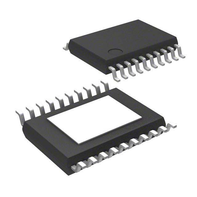
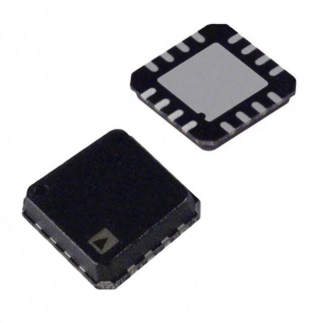
| 供应商器件封装 | 20-VQFN (5x5) |
| 共模抑制比—最小值 | 100 dB |
| 其它名称 | 296-19535-2 |
| 包装 | 带卷 (TR) |
| 单位重量 | 70 mg |
| 单电源电压 | 10 V to 40 V |
| 商标 | Texas Instruments |
| 安装类型 | 表面贴装 |
| 安装风格 | SMD/SMT |
| 封装 | Reel |
| 封装/外壳 | 20-VQFN 裸露焊盘 |
| 封装/箱体 | VQFN-20 |
| 工厂包装数量 | 250 |
| 接口 | - |
| 最大工作温度 | + 125 C |
| 最小工作温度 | - 55 C |
| 标准包装 | 250 |
| 电流-电源 | 25mA |
| 类型 | 输出驱动器 |
| 系列 | XTR300 |
| 输入类型 | 电压 |
| 输入补偿电压 | 1.8 mV |
| 输出类型 | 电流 |
| 配用 | /product-detail/zh/XTR300EVM/296-19618-ND/1014193 |


- 商务部:美国ITC正式对集成电路等产品启动337调查
- 曝三星4nm工艺存在良率问题 高通将骁龙8 Gen1或转产台积电
- 太阳诱电将投资9.5亿元在常州建新厂生产MLCC 预计2023年完工
- 英特尔发布欧洲新工厂建设计划 深化IDM 2.0 战略
- 台积电先进制程称霸业界 有大客户加持明年业绩稳了
- 达到5530亿美元!SIA预计今年全球半导体销售额将创下新高
- 英特尔拟将自动驾驶子公司Mobileye上市 估值或超500亿美元
- 三星加码芯片和SET,合并消费电子和移动部门,撤换高东真等 CEO
- 三星电子宣布重大人事变动 还合并消费电子和移动部门
- 海关总署:前11个月进口集成电路产品价值2.52万亿元 增长14.8%


PDF Datasheet 数据手册内容提取
XTR300 XTR300 www.ti.com SBOS336C–JUNE2005–REVISEDJUNE2011 Industrial Analog Current/Voltage OUTPUT DRIVER CheckforSamples:XTR300 FEATURES 1 APPLICATIONS • USER-SELECTABLE:VoltageorCurrent 2 Output • PLCOUTPUTPROGRAMMABLEDRIVER • +40VSUPPLYVOLTAGE • INDUSTRIALCROSS-CONNECTORS • V :±10V(upto ±17.5Vat ±20Vsupply) • INDUSTRIALHIGH-VOLTAGEI/O OUT • I :±20mA(linearupto±24mA) • 3-WIRE-SENSORCURRENTORVOLTAGE OUT OUTPUT • SHORT-OROPEN-CIRCUITFAULT INDICATORPIN • ±10V2-AND4-WIREVOLTAGEOUTPUT • NOCURRENTSHUNTREQUIRED U.S. Patent Nos. 7,427,898, 7,425,848, and 7,449,873 • OUTPUTDISABLEFORSINGLEINPUTMODE OtherPatentsPending • THERMALPROTECTION space • OVERCURRENTPROTECTION space • SEPARATEDRIVERANDRECEIVER DESCRIPTION CHANNELS The XTR300 is a complete output driver for industrial • DESIGNEDFORTESTABILITY and process control applications. The output can be CC configured as current or voltage by the digital I/V select pin. No external shunt resistor is required. Only external gain-setting resistors and a loop compensationcapacitorarerequired. XTR300 V+ V- The separate driver and receiver channels provide IMON Current Copy flexibility. The Instrumentation Amplifier (IA) can be R1kIMWON ICOPY used for remote voltage sense or as a high-voltage, IDRV high-impedance measurement channel. In voltage Input Signal VIN output mode, a copy of the output current is provided, DRV (Optional) SET OPA allowingcalculationofloadresistance. IAIN+ The digital output selection capability, together with ROS RSET IIA RG1 the error flags and monitor pins, make remote VREF GND1 IA RG2 RGAIN Load ccoonnfdigituiornastioonn tahnedouttrpouutbalensdhooontinthge IpAosinspibulet.asFwauelltl IAOUT IAIN- GND2 as over-temperature conditions are indicated by the RIA OD EFCM error flags. The monitoring pins provide continuous 1kW M1 Digital Error EFLD feedback about load power or impedance. For M2 Control Flags EFOT additional protection, the maximum output current is GND3 DGND limitedandthermalprotectionisprovided. Figure1. XTR300BasicDiagram The XTR300 is specified over the −40°C to +85°C industrial temperature range and for supply voltages upto40V. 1 Pleasebeawarethatanimportantnoticeconcerningavailability,standardwarranty,anduseincriticalapplicationsofTexas Instrumentssemiconductorproductsanddisclaimerstheretoappearsattheendofthisdatasheet. Alltrademarksarethepropertyoftheirrespectiveowners. 2 PRODUCTIONDATAinformationiscurrentasofpublicationdate. Copyright©2005–2011,TexasInstrumentsIncorporated Products conform to specifications per the terms of the Texas Instruments standard warranty. Production processing does not necessarilyincludetestingofallparameters.
XTR300 SBOS336C–JUNE2005–REVISEDJUNE2011 www.ti.com This integrated circuit can be damaged by ESD. Texas Instruments recommends that all integrated circuits be handled with appropriateprecautions.Failuretoobserveproperhandlingandinstallationprocedurescancausedamage. ESDdamagecanrangefromsubtleperformancedegradationtocompletedevicefailure.Precisionintegratedcircuitsmaybemore susceptibletodamagebecauseverysmallparametricchangescouldcausethedevicenottomeetitspublishedspecifications. ORDERINGINFORMATION(1) PACKAGE PRODUCT PACKAGE-LEAD DESIGNATOR PACKAGEMARKING XTR300 QFN-20(5mmx5mm) RGW XTR300 (1) Forthemostcurrentpackageandorderinginformation,seethePackageOptionAddendumattheendofthisdocument,orseethe deviceproductfolderatwww.ti.com. ABSOLUTE MAXIMUM RATINGS(1) Overoperatingfree-airtemperaturerange(unlessotherwisenoted). XTR300 UNIT SupplyVoltage,VVSP +44 V SignalInputTerminals: Voltage(2) (V−)−0.5to(V+)+0.5 V Current(2) ±25 mA DGND ±25 mA OutputShort-Circuit(3) Continuous OperatingTemperature –55to+125 °C StorageTemperature –55to+125 °C JunctionTemperature +150 °C ElectrostaticDischargeRatings: HumanBodyModel(HBM) 2000 V ChargedDeviceModel(CDM) 1000 V (1) Stressesabovetheseratingsmaycausepermanentdamage.Exposuretoabsolutemaximumconditionsforextendedperiodsmay degradedevicereliability.Thesearestressratingsonly,andfunctionaloperationofthedeviceattheseoranyotherconditionsbeyond thosespecifiedisnotsupported. (2) Inputterminalsarediode-clampedtothepower-supplyrails.Inputsignalsthatcanswingmorethan0.5Vbeyondthesupplyrailsmust becurrentlimited.DRVpinallowsapeakcurrentof50mA.SeetheOutputProtectionsectioninApplicationsInformation. (3) SeetheDriverOutputDisablesectioninApplicationsInformationforthermalprotection. 2 Copyright©2005–2011,TexasInstrumentsIncorporated
XTR300 www.ti.com SBOS336C–JUNE2005–REVISEDJUNE2011 ELECTRICAL CHARACTERISTICS: VOLTAGE OUTPUT MODE Boldfacelimitsapplyoverthespecifiedtemperaturerange:T =–40°Cto+85°C. A AllspecificationsatT =+25°C,V =±20V,R =800Ω,R =2kΩ,R =2kΩ,V =4V,R =10kΩ,InputSignal A S LOAD SET OS REF GAIN Span0Vto4V,andC =100pF,unlessotherwisenoted. C XTR300 PARAMETER CONDITIONS MIN TYP MAX UNIT OFFSETVOLTAGE OffsetVoltage,RTI VOS ±0.4 ±1.9 mV vsTemperature dVOS/dT ±1.6 ±6 μV/°C vsPowerSupply PSRR VS=±5Vto±22V ±0.2 ±10 μV/V INPUTVOLTAGERANGE NominalSetupfor±10VOutput SeeFigure2 InputVoltageforLinearOperation (V−)+3V (V+)−3V V NOISE VoltageNoise,f=0.1Hzto10Hz,RTI 3 μVPP VoltageNoiseDensity,f=1kHz,RTI en 40 nV/√Hz OUTPUT VoltageOutputSwingfromRail IDRV≤15mA (V−)+3 (V+)−3 V GainNonlinearity ±0.01 ±0.1 %FS vsTemperature ±0.1 ±1 ppm/°C GainError IB ±0.04 ±0.1 %FS vsTemperature ±0.2 ±1 ppm/°C OutputImpedance,dVDRV/dIDRV 7 mΩ OutputLeakageCurrentWhileOutputDisabled PinOD=L(1) 30 nA Short-CircuitCurrent ISC ±15 ±20 ±24 mA CapacitiveLoadDrive CLOAD CC=10nF,RC=15(2) 1 μF RejectionofVoltageDifferencebetweenGND1and 130 dB GND2,RTO FREQUENCYRESPONSE Bandwidth(3) −3dB G=5 300 kHz SlewRate(2) SR 1 V/μs SR CC=10nF,CL=1μF,RC=15Ω 0.015 V/μs SettlingTime(2)(4),0.1%,SmallSignal VDRV=±1V 8 μs OverloadRecoveryTime 50%Overdrive 12 μs (1) OutputleakageincludesinputbiascurrentofINA. (2) RefertoDrivingCapacitiveLoadssectioninApplicationsInformation. (3) Smallsignalwithnocapacitiveload. (4) 8μsplusnumberofchoppingperiods.SeeApplicationsInformation,InternalCurrentSourcesandSettlingTimesection. Copyright©2005–2011,TexasInstrumentsIncorporated 3
XTR300 SBOS336C–JUNE2005–REVISEDJUNE2011 www.ti.com ELECTRICAL CHARACTERISTICS: CURRENT OUTPUT MODE Boldfacelimitsapplyoverthespecifiedtemperaturerange:T =–40°Cto+85°C. A AllspecificationsatT =+25°C,V =±20V,R =800Ω,R =2kΩ,R =2kΩ,V =4V,InputSignalSpan0to4V,and A S LOAD SET OS REF C =100pF,unlessotherwisenoted. C XTR300 PARAMETER CONDITIONS MIN TYP MAX UNIT OFFSETVOLTAGE InputOffsetVoltage VOS OutputCurrent<1μA ±0.4 ±1.8 mV vsTemperature dVOS/dT ±1.5 ±6 μV/°C vsPowerSupply PSRR VS=±5Vto±22V ±0.2 ±10 μV/V INPUTVOLTAGERANGE NominalSetupfor±20mAOutput SeeFigure3 MaximumInputVoltageforLinearOperation (V−)+3V (V+)−3V V NOISE VoltageNoise,f=0.1Hzto10Hz,RTI 3 μVPP VoltageNoiseDensity,f=1kHz,RTI en 33 nV/√Hz OUTPUT ComplianceVoltageSwingfromRail IDRV=±24mA (V−)+3 (V+)−3 V OutputConductance(dIDRV/dVDRV) dVDRV=±15V,dIDRV=±24mA 0.7 μA/V Transconductance SeeTransferFunctioninFigure3 GainError IDRV=±24mA ±0.04 ±0.12 %FS vsTemperature IDRV=±24mA ±3.6 ±10 ppm/°C LinearityError IB IDRV=±24mA ±0.01 ±0.1 %FS vsTemperature IDRV=±24mA ±1.5 ±6 ppm/°C OutputLeakageCurrentWhileOutputDisabled PinOD=L 0.6 nA Short-CircuitCurrent ISC ±24.5 ±32 ±38.5 mA CapacitiveLoadDrive(1)(2) CLOAD 1 μF FREQUENCYRESPONSE Bandwidth −3dB 160 kHz SlewRate(2) SR 1.3 mA/μs SettlingTime(2)(3),0.1%,SmallSignal IDRV=±2mA 8 μs OverloadRecoveryTime CLOAD=0,50%Overdrive 1 μs (1) RefertoDrivingCapacitiveLoadssectioninApplicationsInformation. (2) Withcapacitiveload,theslewratecanbelimitedbytheshortcircuitcurrentandtheloaderrorflagcantriggerduringslewing. (3) 8μsplusnumberofchoppingperiods.SeeApplicationsInformation,InternalCurrentSourcesandSettlingTimesection. 4 Copyright©2005–2011,TexasInstrumentsIncorporated
XTR300 www.ti.com SBOS336C–JUNE2005–REVISEDJUNE2011 ELECTRICAL CHARACTERISTICS: OPERATIONAL AMPLIFIER (OPA) Boldfacelimitsapplyoverthespecifiedtemperaturerange:T =–40°Cto+85°C. A AllspecificationsatT =+25°C,V =±20V,andR =800Ω,unlessotherwisenoted. A S LOAD XTR300 PARAMETER CONDITIONS MIN TYP MAX UNIT OFFSETVOLTAGE OffsetVoltage,RTI VOS IDRV=0A ±0.4 ±1.8 mV Drift dVOS/dT ±1.5 μV/°C vsPowerSupply PSRR VS=±5Vto±22V ±0.2 ±5 μV/V INPUTVOLTAGERANGE Common-ModeVoltageRange VCM (V−)+3 (V+)−3 V Common-ModeRejectionRatio CMRR (V−)+3V<VCM<(V+)−3V 100 126 dB INPUTBIASCURRENT InputBiasCurrent IB ±20 ±35 nA InputOffsetCurrent IOS ±0.3 ±10 nA INPUTIMPEDANCE Differential 108||5 Ω||pF Common-Mode 108||5 Ω||pF OPEN-LOOPGAIN Open-LoopVoltageGain AOL (V−)+3V<VDRV<(V+)−3V,IDRV=±24mA 100 126 dB OUTPUT VoltageOutputSwingfromRail IDRV=±24mA (V−)+3 (V+)−3 V Short-CircuitCurrent ILIMIT M2=High ±25.5 ±32 ±38.5 mA ILIMIT M2=Low ±16 ±20 ±24 mA OutputLeakageCurrentWhileOutput Disabled ILEAK_DRV PinOD=L 10 pA FREQUENCYRESPONSE Gain-BandwidthProduct GBW G=1 2 MHz SlewRate SR 1 V/μs Copyright©2005–2011,TexasInstrumentsIncorporated 5
XTR300 SBOS336C–JUNE2005–REVISEDJUNE2011 www.ti.com ELECTRICAL CHARACTERISTICS: INSTRUMENTATION AMPLIFIER (IA) Boldfacelimitsapplyoverthespecifiedtemperaturerange:T =–40°Cto+85°C. A AllspecificationsatT =+25°C,V =±20V,R =2kΩ,andR =2kΩ,unlessotherwisenoted.SeeFigure4. A S IA GAIN XTR300 PARAMETER CONDITIONS MIN TYP MAX UNIT OFFSETVOLTAGE OffsetVoltage,RTI VOS IDRV=0A ±0.7 ±2.7 mV vsTemperature dVOS/dT ±2.4 ±10 μV/°C vsPowerSupply PSRR VS=±5Vto±22V ±0.8 ±10 μV/V INPUTVOLTAGERANGE InputVoltageRange VCM (V−)+3 (V+)−3 V Common-ModeRejectionRatio CMRR RTI 100 130 dB INPUTBIASCURRENT InputBiasCurrent IB ±20 ±35 nA InputOffsetCurrent IOS ±1 ±10 nA INPUTIMPEDANCE Differential 105||5 Ω||pF Common-Mode 105||5 Ω||pF TRANSCONDUCTANCE(Gain) IAOUT=2(IAIN+−IAIN−)/RGAIN TransconductanceError IAOUT=±2.4mA,(V−)+3V<VIAOUT<(V+)− ±0.04 ±0.1 %/FS 3V vsTemperature ±0.2 ppm/°C LinearityError (V−)+3V<VIAOUT<(V+)−3V ±0.01 ±0.1 %FS InputBiasCurrenttoG1,G2 ±20 nA InputOffsetCurrenttoG1,G2(1) ±1 nA OUTPUT OutputSwingtotheRail IAOUT=±2.4mA (V−)+3 (V+)−3 V OutputImpedance IAOUT=±2.4mA 600 mΩ Short-CircuitCurrent ILIMIT M2=High ±7.2 mA ILIMIT M2=Low ±4.5 mA FREQUENCYRESPONSE Gain-BandwidthProduct GBW G=1,RGAIN=10kΩ,RIA=5kΩ 1 MHz SlewRate SR G=1,RGAIN=10kΩ,RIA=5kΩ 1 V/μs SettlingTime(2),0.1% IAOUT=±40μA,RGAIN=10kΩ,RIA=5kΩ,CL= 6 μs 100pF OverloadRecoveryTime,50% RGAIN=10kΩ,RIA=15kΩ,CL=100pF 10 μs (1) SeeTypicalCharacteristicscurve(Figure7). (2) 6μsplusnumberofchoppingperiods.SeeApplicationsInformation,InternalCurrentSourcesandSettlingTimesection. 6 Copyright©2005–2011,TexasInstrumentsIncorporated
XTR300 www.ti.com SBOS336C–JUNE2005–REVISEDJUNE2011 ELECTRICAL CHARACTERISTICS: CURRENT MONITOR Boldfacelimitsapplyoverthespecifiedtemperaturerange:T =–40°Cto+85°C. A AllspecificationsatT =+25°CandV =±20V,unlessotherwisenoted.SeeFigure4. A S XTR300 PARAMETER CONDITIONS MIN TYP MAX UNIT OUTPUT OffsetCurrent IOS IDRV=0A ±30 ±100 nA Drift dIOS/dT ±0.05 nA/°C vsPowerSupply PSRR VS=±5Vto±22V ±0.1 ±10 nA/V MonitorOutputSwingtotheRail IMON=±2.4mA (V−)+3 (V+)−3 V MonitorOutputImpedance IMON=±2.4mA 200 MΩ MONITORCURRENTGAIN IMON=IDRV/10 CurrentGainError IDRV=±24mA ±0.04 ±0.12 %FS vsTemperature IDRV=±24mA ±3.6 ppm/°C LinearityError IDRV=±24mA ±0.01 ±0.1 %FS vsTemperature IDRV=±24mA ±1.5 ppm/°C ELECTRICAL CHARACTERISTICS Boldfacelimitsapplyoverthespecifiedtemperaturerange:T =–40°Cto+85°C. A AllspecificationsatT =+25°CandV =±20V,unlessotherwisenoted.SeeFigure4. A S XTR300 PARAMETER CONDITIONS MIN TYP MAX UNIT POWERSUPPLY SpecifiedVoltageRange VS ±5 ±20 V OperatingVoltageRange ±5 ±22 V QuiescentCurrent IQ IDRV=IAOUT=0A 1.8 2.3 mA OverTemperature 2.8 mA TEMPERATURERANGE SpecifiedTemperatureRange −40 +85 °C OperatingTemperatureRange −55 +125(1) °C StorageTemperatureRange −55 +125 °C ThermalResistance Junction-to-Case θJC 15.2 °C/W Junction-to-Ambient θJA 38 °C/W THERMALFLAG(EFOT)Output Alarm(EFOTpinLOW) 140 °C ReturntoNormalOperation(EFOTpinHIGH) 125 °C DIGITALINPUTS(M1,M2,OD) VILLow-LevelInputVoltage ≤0.8 V VIHHigh-LevelInputVoltage >1.4 V InputCurrent ±1 μA DIGITALOUTPUTS(EFLD,EFCM,EFOT) IOHHigh-LevelLeakageCurrent(Open-Drain) −1.2 μA VOLLow-LevelOutputVoltage IOL=5mA 0.8 V VOLLow-LevelOutputVoltage IOL=2.8mA 0.4 V DIGITALGROUNDPIN (V−)≤DGND≤(V+)−7V CurrentInput M1=M2=L,OD=H,AllDigitalOutputsH −25 μA (1) EF notconnectedwithOD. OT Copyright©2005–2011,TexasInstrumentsIncorporated 7
XTR300 SBOS336C–JUNE2005–REVISEDJUNE2011 www.ti.com FUNCTIONAL BLOCK DIAGRAMS C C XTR300 V+ V- I Current Copy MON R1kIMWON ICOPY I Input Signal DRV VIN= 0V to 4.0V GND3 VIN DRV OPA SET IAIN+ Transfer Function: ROS RSET IIA RG1 V = RGAIN( V I N + V IN - V R EF ) IA RG RGAIN Load OUT 2 RSET ROS 2 V =4.0V REF IA IAIN- OUT H OD EFCM L M1 Digital Error EFLD L M2 Control Flags EFOT DGND DV GND GND1 GND2 Figure2. StandardCircuitforVoltageOutputMode C C XTR300 V+ V- I Current Copy MON I COPY I Input Signal DRV VIN= 0V to 4.0V VIN DRV OPA SET Transfer Function: IAIN+ ( V V -V ( ROS RSET IIA RG1 IOUT= 10 RSIENT + INROSREF IA RG 2 V =4.0V REF IA IAIN- OUT I H OD EFCM OUT L M1 Digital Error EFLD H M2 Control Flags EFOT DGND GND1 GND2 Figure3. StandardCircuitforCurrentOutputMode 8 Copyright©2005–2011,TexasInstrumentsIncorporated
XTR300 www.ti.com SBOS336C–JUNE2005–REVISEDJUNE2011 Feedback Network XTR300 V+ V- I Current Copy MON I COPY I DRV GND3 V IN Input Signal OPA DRV SET IA IN+ RSET IIA RG 1 IA RGAIN RG GND1 2 IA IAIN- OUT R OD EFCM IA H M1 Digital Error EFLD M2 Control Flags EFOT DGND GND3 Figure4. StandardCircuitforExternallyConfiguredMode Copyright©2005–2011,TexasInstrumentsIncorporated 9
XTR300 SBOS336C–JUNE2005–REVISEDJUNE2011 www.ti.com PIN CONFIGURATIONS RGWPACKAGE QFN-20 (TOPVIEW) D D FOT FLD FCM GN O E E E D 20 19 18 17 16 M2 1 Exposed 15 V+ Thermal M1 2 Die Pad 14 NC on V 3 13 DRV IN Underside SET 4 (must be 12 NC connected I 5 to V-) 11 V- MON 6 7 8 9 10 Pad UT -N N+ G1 G2 IAO IAI IAI R R PIN ASSIGNMENTS PINNO. NAME FUNCTION 1 M2 ModeInput 2 M1 ModeInput 3 V NoninvertingSignalInput IN 4 SET InputforGainSetting;InvertingInput 5 I CurrentMonitorOutput MON 6 IA InstrumentationAmplifierSignalOutput OUT 7 IA InstrumentationAmplifierInvertingInput IN– 8 IA InstrumentationAmplifierNoninvertingInput IN+ 9 RG1 InstrumentationAmplifierGainResistor 10 RG2 InstrumentationAmplifierGainResistor 11 V– NegativePowerSupply 12 NC NoInternalConnection 13 DRV OperationalAmplifierOutput 14 NC NoInternalConnection 15 V+ PositivePowerSupply 16 DGND GroundforDigitalI/O 17 EF ErrorFlagforCommon-ModeOver-Range,ActiveLow CM 18 EF ErrorFlagforLoadError,ActiveLow LD 19 EF ErrorFlagforOverTemperature,ActiveLow OT 20 OD OutputDisable,DisabledLow Pad ExposedPad ExposedthermalpadmustbeconnectedtoV− 10 Copyright©2005–2011,TexasInstrumentsIncorporated
XTR300 www.ti.com SBOS336C–JUNE2005–REVISEDJUNE2011 TYPICAL CHARACTERISTICS AtT =+25°CandV+=±20V,unlessotherwisenoted. A QUIESCENTCURRENTvsTEMPERATURE QUIESCENTCURRENTvsSUPPLYVOLTAGE 3.0 1.90 1.88 2.5 1.86 1.84 2.0 1.82 A) A) m 1.5 m 1.80 ( ( Q Q I I 1.78 1.0 1.76 1.74 0.5 1.72 0 1.70 -50 -25 0 25 50 75 100 125 10 15 20 25 30 35 40 45 Temperature (°C) Total Supply Voltage (V) Figure5. Figure6. INPUTBIASCURRENTvsTEMPERATURE (V ,SET,IA ,IA ,RG1,RG2) OPAOUTPUTSWINGTORAILvsTEMPERATURE IN IN+ IN− 0 2.2 I = +24mA -5 2.0 IDRV=-24mA DRV I = +20mA -10 V) 1.8 DRV ( (nA)B -15 V½OUT 1.6 I = +10mA I - DRV -20 VS 1.4 ½ IDRV=-20mA IDRV=-10mA -25 1.2 -30 1.0 -50 -25 0 25 50 75 100 125 -50 -25 0 25 50 75 100 125 Temperature (°C) Temperature (°C) Figure7. Figure8. OPAGAINANDPHASEvsFREQUENCY IAGAINANDPHASEvsFREQUENCY 180 0 80 0 160 -20 RGAIN= 10kW 140 -40 60 -45 120 Phase -60 40 RIA= 500kW -90 Gain (dB) 1086000 ---81100200 Phase ()° Gain (dB) 20 RIA= 50kRWIA= 10kW -135 Phase ()° 40 -140 0 R = 5kW -180 Gain IA 20 -160 -20 -225 0 -180 Gain RIA= 1kW Phase -20 -200 -40 -270 0.0010.01 0.1 1 10 100 1k 10k 100k 1M 10M 1 10 100 1k 10k 100k 1M 10M Frequency (Hz) Frequency (Hz) Figure9. Figure10. Copyright©2005–2011,TexasInstrumentsIncorporated 11
XTR300 SBOS336C–JUNE2005–REVISEDJUNE2011 www.ti.com TYPICAL CHARACTERISTICS (continued) AtT =+25°CandV+=±20V,unlessotherwisenoted. A OPACMRRANDPSRRvsFREQUENCY IACMRRANDPSRRvsFREQUENCY 160 140 140 120 120 dB) dB) 100 PSRR+ RR ( 100 PSRR- RR ( 80 PS 80 PS PSRR- R, R, 60 R 60 R M PSRR+ M CMRR C C 40 40 CMRR 20 20 0 0 1 10 100 1k 10k 100k 1 10 100 1k 10k 100k Frequency (Hz) Frequency (Hz) Figure11. Figure12. SMALL−SIGNALSTEPRESPONSE LARGE−SIGNALSTEPRESPONSE CURRENTMODE CURRENTMODE v di v 00mV/ IGO U=T 8=±200mA 10V/di IGO U=T 8=±20mA 1 CL= 100nF || RL= 800W CL= 100nF || RL= 800W CC= 4.7nF CC= 4.7nF RSET= 1kW RSET= 1kW RGAIN= 10kW RGAIN= 10kW See Figure 3 See Figure 3 200ms/div 200ms/div Figure13. Figure14. SMALL−SIGNALSTEPRESPONSE LARGE−SIGNALSTEPRESPONSE VOLTAGEMODE VOLTAGEMODE v di v mV/ V/di 50 G = 5 5 G = 5 C = 100nF || R = 800W C = 100nF || R = 800W L L L L C = 4.7nF C = 4.7nF C C R = 1kW R = 1kW SET SET R = 10kW R = 10kW GAIN GAIN See Figure 2 See Figure 2 200ms/div 200ms/div Figure15. Figure16. 12 Copyright©2005–2011,TexasInstrumentsIncorporated
XTR300 www.ti.com SBOS336C–JUNE2005–REVISEDJUNE2011 TYPICAL CHARACTERISTICS (continued) AtT =+25°CandV+=±20V,unlessotherwisenoted. A INPUT−REFERREDNOISESPECTRUM INPUT−REFERRED0.1Hzto10HzNOISE VOLTAGEOUTPUTMODE VOLTAGEOUTPUTMODE 1M G = 5 100k )z 10k H ÖnV/ 1k V/div e ( 1m s oi N 100 10 1 1s/div 1 10 100 1k 10k 100k Frequency (Hz) Figure17. Figure18. INPUT−REFERREDNOISESPECTRUM INPUT−REFERRED0.1Hzto10HzNOISE CURRENTOUTPUTMODE CURRENTOUTPUTMODE 1M G = 10 )Hz 100k Ö V/ e (n 10k d Nois 1k V/divm e 1 err ef 100 R ut- p 10 n I 1 1s/div 1 10 100 1k 10k 100k Frequency (Hz) Figure19. Figure20. IAINPUT−REFERREDNOISESPECTRUM IAINPUT−REFERRED0.1Hzto10HzNOISE 1M G = 20 )z 100k H Ö V/ e (n 10k s v oi di d N 1k V/m e 1 err ef 100 R ut- np 10 I 1 1s/div 1 10 100 1k 10k 100k Frequency (Hz) Figure21. Figure22. Copyright©2005–2011,TexasInstrumentsIncorporated 13
XTR300 SBOS336C–JUNE2005–REVISEDJUNE2011 www.ti.com TYPICAL CHARACTERISTICS (continued) AtT =+25°CandV+=±20V,unlessotherwisenoted. A OPAOFFSETVOLTAGEDISTRIBUTION IAOFFSETVOLTAGEDISTRIBUTION 18 30 16 25 %) 14 %) Percent of Population ( 1120864 Percent of Population ( 211050 5 2 0 0 -2.0 -1.6 -1.2 -0.8 -0.4 0 0.4 0.8 1.2 1.6 2.0 -3.0 -2.4 -1.8 -1.2 -0.6 0 0.6 1.2 1.8 2.4 3.0 Offset Voltage (mV) Offset Voltage (mV) Figure23. Figure24. OPAOFFSETVOLTAGEDRIFTDISTRIBUTION IAOFFSETVOLTAGEDRIFTDISTRIBUTION 60 40 35 50 on (%) 40 on (%) 30 ati ati 25 ul ul Pop 30 Pop 20 Percent of 20 Percent of 1150 10 5 0 0 -10 -8 -6 -4 -2 0 2 4 6 8 10 -10 -8 -6 -4 -2 0 2 4 6 8 10 Offset Voltage Drift (mV/°C) Offset Voltage Drift (mV/°C) Figure25. Figure26. VOLTAGEMODEGAINERRORDISTRIBUTION CURRENTMODEGAINERRORDISTRIBUTION 40 30 35 25 %) 30 %) on ( on ( 20 ati 25 ati ul ul op 20 op 15 P P nt of 15 nt of 10 e e erc 10 erc P P 5 5 0 0 0 0 0 0 0 0 0 0 0 0 0 0 0 0 0 0 0 0 0 0 0 0 0 0 0 0 0 0 0 0 0 0 0 0 0 0 0 0 0 0 0 0 0 8 6 4 2 2 4 6 8 0 0 8 6 4 2 2 4 6 8 0 1 - - - - 1 1 - - - - 1 - - Gain Error (ppm) Gain Error (ppm) Figure27. Figure28. 14 Copyright©2005–2011,TexasInstrumentsIncorporated
XTR300 www.ti.com SBOS336C–JUNE2005–REVISEDJUNE2011 TYPICAL CHARACTERISTICS (continued) AtT =+25°CandV+=±20V,unlessotherwisenoted. A VOLTAGEMODENONLINEARITYDISTRIBUTION CURRENTMODENONLINEARITYDISTRIBUTION 60 60 50 50 %) %) on ( 40 on ( 40 ati ati ul ul op 30 op 30 P P of of nt 20 nt 20 e e c c er er P P 10 10 0 0 -1000 -800 -600 -400 -200 0 200 400 600 800 1000 -1000 -800 -600 -400 -200 0 200 400 600 800 1000 Nonlinearity (ppm) Nonlinearity (ppm) Figure29. Figure30. VOLTAGEMODEGAINERRORDRIFTDISTRIBUTION CURRENTMODEGAINERRORDRIFTDISTRIBUTION 70 60 60 50 %) %) Population ( 5400 Population ( 4300 Percent of 3200 Percent of 20 10 10 0 0 1.0 0.8 0.6 0.4 0.2 0 0.2 0.4 0.6 0.8 1.0 10 -8 -6 -4 -2 0 2 4 6 8 10 - - - - - - Gain Error Drift (ppm/°C) Gain Error Drift (ppm/°C) Figure31. Figure32. VOLTAGEMODENONLINEARITYDRIFTDISTRIBUTION CURRENTMODENONLINEARITYDRIFTDISTRIBUTION 80 100 70 90 %) 60 %) 80 n ( n ( 70 o o ati 50 ati 60 ul ul op 40 op 50 P P nt of 30 nt of 40 erce 20 erce 30 P P 20 10 10 0 0 0 8 6 4 2 0 2 4 6 8 0 0 8 6 4 2 0 2 4 6 8 0 -1. -0. -0. N-0.onlin-e0.arity Drift (0.ppm/°0.C) 0. 0. 1. -1 - - N-onlin-earity Drift (ppm/°C) 1 Figure33. Figure34. Copyright©2005–2011,TexasInstrumentsIncorporated 15
XTR300 SBOS336C–JUNE2005–REVISEDJUNE2011 www.ti.com TYPICAL CHARACTERISTICS (continued) AtT =+25°CandV+=±20V,unlessotherwisenoted. A POSITIVECURRENTLIMITvsTEMPERATURE NEGATIVECURRENTLIMITvsTEMPERATURE 36 -16 34 -18 Voltage Mode 32 Current Mode -20 30 -22 A) 28 A) -24 m m ( 26 ( -26 ILIMIT 24 ILIMIT -28 22 Voltage Mode -30 20 -32 Current Mode 18 -34 16 -36 -50 -25 0 25 50 75 100 125 -50 -25 0 25 50 75 100 125 Temperature (°C) Temperature (°C) Figure35. Figure36. NONLINEARITYvsOUTPUTCURRENT NONLINEARITYvsOUTPUTCURRENT (±24mAEndPointCalibration) (±20mAEndPointCalibration) 0.025 0.025 +25°C -55°C +25°C -55°C 0 0 %) %) arity ( -0.025 +85°C arity ( -0.025 +125°C +85°C e e nlin -0.050 nlin -0.050 o o N N -0.075 -0.075 +125°C -0.100 -0.100 -24 -20 -16 -12 -8 -4 0 4 8 12 16 20 24 -24 -20 -16 -12 -8 -4 0 4 8 12 16 20 24 Output Current (mA) Output Current (mA) Figure37. Figure38. 16 Copyright©2005–2011,TexasInstrumentsIncorporated
XTR300 www.ti.com SBOS336C–JUNE2005–REVISEDJUNE2011 APPLICATION INFORMATION V+ V- GND C 2 100nF C 3 C 100nF C 47nF GND1 XTR300 V+ V- Thermal Pad(2) I Current Copy I MON MON I R COPY S 1kW3 VIN IDRV RC External Load IN 15W R DRV OS OPA 2kW C SET 4 OS 100nF R 6 2.2kW RIMON RSET IAIN+ GND1 1kW 2kW IIA RG CLOAD RLOAD SG GND1 IA RG21 R10GkAWIN C105nF 2.R2k7W IA O IAOUT IAIN- GND2 R OD EFCM 1kIWA M1 Digital Error EFLD Logic Supply M2 Control Flags EFOT (+2.7V to +5V) DGND (1) GND3 Pull-up Resistors GND4 (10kW) (1) SeetheElectricalCharacteristicsandDigitalInputandOutputsectionforoperatinglimitsofDGND. (2) ConnectthermalpadtoV−. Figure39. StandardCircuitConfiguration ThefollowinginformationshouldbeconsideredduringXTR300circuitconfiguration: space • R ensures stability for unknown load conditions • Recommended bypassing: 100nF or more for C and limits the current into the internal protection supplybypassingateachsupply. diodes. C helps protect the device. Over-voltage 4 • RIMON can be in the kΩ-range or short-circuited if clamp diodes (standard 1N4002) might be not used. Do not leave this current output necessarytoprotecttheoutput. unconnected—it would saturate the internal • R ,R ,andC protecttheIA. current source. The current at this I output is 6 7 5 MON • R and C represent the load resistance I /10.Therefore,V =R (I /10). LOAD LOAD DRV IMON IMON DRV andloadcapacitance. • R is not required but can match R (or 3 SET • R defines the transfer gain. It can be split to R ||R )tocompensateforthebiascurrent. SET SET OS allow a signal offset and, therefore, allow a 5V • R canbeshort-circuitedifnotused.Donotleave IA single-supply digital-to-analog converter (DAC) to this current output unconnected. R is selected GAIN controla±10Vor ±20mAoutputsignal. to 10kΩ to match the output of 10V with 20mA for theequalinputsignal. space space space Copyright©2005–2011,TexasInstrumentsIncorporated 17
XTR300 SBOS336C–JUNE2005–REVISEDJUNE2011 www.ti.com The XTR300 can be used with asymmetric supply voltages; however, the minimum negative supply voltage shouldbeequaltoormorenegativethan−3V(typically−5V).Thissupplyvalueensurespropercontrolof0Vand 0mA with wire resistance, ground offsets, and noise added to the output. For positive output signals, the current requirementfromthisnegativevoltagesourceislessthan5mA. GND1 through GND4 must be selected to fulfill specified operating ranges. DGND must be in the range of (V−) ≤ DGND≤ (V+) −7V. Builtonarobusthigh-voltageBiCMOSprocess,theXTR300isdesignedtointerfacethe5Vor3Vsupplydomain used for processors, signal converters, and amplifiers to the high-voltage and high-current industrial signal environment. It is specified for up to ±20V supply, but can also be powered asymmetrically (for example, +24V and−5V).Itisdesignedtoallowinsertionofexternalcircuitprotectionelementsanddrivelargecapacitiveloads. FUNCTIONAL FEATURES The XTR300 provides two basic functional blocks: an instrumentation amplifier (IA) and a driver that is a unique operational amplifier (OPA) for current or voltage output. This combination represents an analog output stage which can be digitally configured to provide either current or voltage output to the same terminal pin. Alternatively,itcanbeconfiguredforindependentmeasurementchannels. Three open collector error signals are provided to indicate output related errors such as over-current or open-load (EF ) or exceeding the common-mode input range at the IA inputs (EF ). An over-temperature flag LD CM (EF ) can be used to control output disable to protect the circuit. The monitor outputs (I and IA ) and the OT MON OUT error flags offer optimal testability during operation and configuration. The I output represents the current MON flowing into the load in voltage output mode, while the IA represents the voltage across the connectors in OUT current output mode. Both monitor outputs can be connected together when used in current or voltage output modebecausethemonitorsignalsaremultiplexedaccordingly. VOLTAGE OUTPUT MODE In voltage output mode (M1 and M2 are connected low or left unconnected), the feedback loop through the IA provides high impedance remote sensing of the voltage at the destination, compensating the resistance of a protection circuit, switches, wiring, and connector resistance. The output of the IA is a current that is proportional to the input voltage. This current is internally routed to the OPA summing junction through a multiplexer, as showninFigure40. A 1:10 copy of the output current of the OPA can be monitored at the I pin. This output current and the MON knownoutputvoltagecanbeusedtocalculatetheloadresistanceorloadpower. During an output short-circuit or an over-current condition the XTR300 output current is limited and EF (load LD error,activelow)flagisactivated. 18 Copyright©2005–2011,TexasInstrumentsIncorporated
XTR300 www.ti.com SBOS336C–JUNE2005–REVISEDJUNE2011 C C XTR300 V+ V- I Current Copy MON I R COPY IMON I DRV Input Signal GND3 V IN DRV OPA SET IA IN+ RSET IIA RG 1 IA RGAIN Load RG 2 GND1 IA IAIN- OUT OD EFCM GND2 L M1 Digital Error EFLD L M2 Control Flags EFOT DGND Figure40. SimplifiedVoltageOutputModeConfiguration Applications not requiring the remote sense feature can use the OPA in stand-alone operation (M1 = high). In thiscase,theIAisavailableasaseparateinputchannel. TheIAgaincanbesetbytworesistors,R andR : GAIN SET R V = GAIN V OUT 2R IN SET (1) orwhenaddinganoffset,V ,togetbidirectionaloutputwithasingle-endedinput: REF R ( V V -V ( V = GAIN IN + IN REF OUT 2 R R SET OS (2) The R resistor is also used in current output mode. Therefore, it is useful to define R for the current mode, SET SET thensettheratiobetweencurrentandvoltagespanwithR . GAIN Copyright©2005–2011,TexasInstrumentsIncorporated 19
XTR300 SBOS336C–JUNE2005–REVISEDJUNE2011 www.ti.com CURRENT OUTPUT MODE The XTR300 does not require a shunt resistor for current control because it uses a precise current mirror arrangement. In current output mode (M1 connected low, or left unconnected and M2 connected high) a precise copy of 1/10th of the output is internally routed back to the summing junction of the OPA through a multiplexer, closing the controlloopfortheoutputcurrent. The OPA driver can deliver more than ±24mA within a wide output voltage range. An open-output condition or high-impedanceloadthatpreventstheflowoftherequiredcurrentactivatestheEF flagandtheIAcanbecome LD overloadedanddrawgreaterthan7mAsaturationcurrent. While in current output mode, a current (I ) that is proportional to the voltage at the IA input is routed to IA IA OUT and can be used to monitor the load voltage. A resistor converts this current into voltage. This arrangement makeslevelshiftingeasy. Alternatively, the IA can be used as an independent monitoring channel. If this output is not used, connect it to GNDtomaintainproperfunctionofthemonitorstage,asshowninFigure41. XTR300 V+ V- I Current Copy MON I COPY I DRV Input Signal V IN DRV OPA SET IA IN+ RSET IIA RG1 IA RGAIN Load RG 2 GND1 IA IAIN- OUT GND2 R OD EFCM IA L M1 Digital Error EFLD H M2 Control Flags EFOT DGND GND3 Figure41. SimplifiedCurrentOutputModeConfiguration Thetransconductance(gain)canbesetbytheresistor,R ,accordingtotheequation: SET 10 I = V OUT R IN SET (3) space orwhenaddinganoffsetV togetbidirectionaloutputwithasingle-endedinput: REF ( V V -V ( I = 10 IN + IN REF OUT R R SET OS (4) 20 Copyright©2005–2011,TexasInstrumentsIncorporated
XTR300 www.ti.com SBOS336C–JUNE2005–REVISEDJUNE2011 INPUT SIGNAL CONNECTION ItispossibletodrivetheXTR300withaunidirectionalinputsignalandstillgetabidirectionaloutputbyaddingan additional resistor, R , and an offset voltage signal, V . It can be a mid-point voltage or a signal to shift the OS REF outputvoltagetoadesiredvalue. This design is illustrated in Figure 42a, Figure 42b, and Figure 42c. As with a normal operational amplifier, there are several options for offset-shift circuits. The input can be connected for inverting or noninverting gain. Unlike many op amp input circuits, however, this configuration uses current feedback, which removes the voltage relationshipbetweenthenoninvertinginputandoutputpotentialbecausethereisnofeedbackresistor. a) Noninverting Input XTR300 V IN (0 to V ) OFFSET OPA V REF 2RkOWS R2kSWET I Feedback b) Noninverting Input XTR300 V IN ( V ) MIDSCALE OPA V MIDSCALE R SET 1kW I Feedback c) Inverting Input (V = V ) REF OFFSET XTR300 V OFFSET OPA V IN (±V ) OFFSET R SET 1kW I Feedback Figure42. CircuitOptionsforOpAmpOutputLevel-Shifting The input bias current effect on the offset voltage can be reduced by connecting a resistor in series with the positive input that matches the approximate resistance at the negative input. This resistor placed close to the inputpinactsasadampingelementandmakesthedesignlesssensitivetoRFnoise.SeeR inFigure39. 3 Copyright©2005–2011,TexasInstrumentsIncorporated 21
XTR300 SBOS336C–JUNE2005–REVISEDJUNE2011 www.ti.com EXTERNALLY-CONFIGURED MODE: OPA AND IA It is possible to use the precision of the operational amplifier (OPA) and instrumentation amplifier (IA) independently from each other by configuring the digital control pins (M1 high). In this mode, the IA output currentisroutedtoIA andthecopyoftheOPAoutputcurrentisroutedtoI ,asshowninFigure4. OUT MON Thismodeallowsexternalconfigurationoftheanalogsignalroutingandfeedbackloop. The current output IA has high input impedance, low offset voltage and drift, and very high common-mode rejection ratio. An external resistor (R ) can be used to convert the output current of the IA (I ) to an output IA IA voltage.Thegainisgivenby: 2 2R I = V or V = IA V IA R IN IA R IN GAIN GAIN (5) The OPA provides low drift and high voltage output swing that can be used like a common operational amplifier by connecting a feedback network around it. In this mode, the copy of the output current is available at the I MON pin (it includes the current into the feedback network). It provides an output current limit for protection, which can be set between two ranges by M2. The error flag indicates an overcurrent condition, as well as indicating driving theoutputintothesupplyrails. Alternatively,thefeedbackcanbeclosedthroughtheI pintocreateaprecisevoltage-to-currentconverter. MON DRIVER OUTPUT DISABLE The OPA output (DRV) can be switched to a high-impedance mode by driving the OD control pin low. This input can be connected to the over-temperature flag, EF , and a pull-up resistor to protect the IC from OT over-temperaturebydisconnectingtheload. TheoutputdisablemodecanbeusedtosenseandmeasurethevoltageattheIAinputpinswithoutloadingfrom the DRV output. This mode allows testing of any voltage present at the I/O connector. However, consider the biascurrentoftheIAinputpins. The digital control inputs, M1 and M2, set the four operation modes of the XTR300 as shown in Table 1. When M1 is asserted low, M2 determines voltage or current mode and the corresponding appropriate current limit (I ) SC setting. When M1 is high, the internal feedback connections are opened; IA and I are both connected to OUT MON theoutputpins;andM2onlydeterminesthecurrentlimit(I )setting. SC M1 and M2 are pulled low internally with 1μA. Terminate these two pins to avoid noise coupling. Output disable (OD) is internally pulled high with approximately 1μA. When connecting OD to EF , a 2.2kΩ pull-up resistor is OT recommended. Table1. SummaryofConfigurationModes(1) M1 M2 MODE DESCRIPTION L L V VoltageOutputMode,I =20mA OUT SC L H I CurrentOutputMode,I =32mA OUT SC H L Ext IAandI onext.pins,I =20A MON SC H H Ext IAandI onext.pins,I =32mA MON SC (1) ODisacontrolpinindependentofM1orM2. 22 Copyright©2005–2011,TexasInstrumentsIncorporated
XTR300 www.ti.com SBOS336C–JUNE2005–REVISEDJUNE2011 DRIVING CAPACITIVE LOADS AND LOOP COMPENSATION For normal operation, the driver OPA and the IA are connected in a closed loop for voltage output. In current outputmode,thecurrentcopyclosestheloopdirectly. In current output mode, loop compensation is not critical, even for large capacitive loads. However, in voltage output mode, the capacitive load, together with the source impedance and the impedance of the protection circuit, generates additional phase lag. The IA input might also be protected by a low-pass filter that influences phaseintheclosedloop. The loop compensation low-pass filter consists of C and the parallel resistance of R and R . For loop C OS SET stability with large capacitive load, the external phase shift has to be added to the OPA phase. With C , the C voltagegainoftheOPAhastoapproachzeroatthefrequencywherethetotalphaseapproaches180° +135°. The best stability for large capacitive loads is provided by adding a small resistor, R (15Ω). See the Output C Protectionsection. An empirical method of evaluation is using a square wave input signal and observing the settling after transients. Use small signal amplitudes only—steep signal edges cause excessive current to flow into the capacitive load and may activate the current limit, which hides or prevents oscillation. A small-signal oscillation can be hidden from large capacitive loads, but observing the I output on an appropriate resistor (use a similar value like MON R ||R )wouldindicatestabilityissues.NotethatnoisepulsesatI duringoverload(EF active)arenormal SET OS MON LD andarecausedbycyclingofthecurrentmirror. The voltage output mode includes the IA in the loop. An additional low-pass filter in the input reverses the phase andthereforeincreasesthesignalbandwidthoftheloop,butalsoincreasesthedelay.Again,loopstabilityhasto beobserved.OverloadingtheIAdisconnectstheclosedloopandtheoutputvoltagerails. INTERNAL CURRENT SOURCES, SWITCHING NOISE, AND SETTLING TIME The accuracy of the current output mode and the dc performance of the IA rely on dynamically-matched current mirrors. Identical current sources are rotated to average out mismatch errors. It can take several clock cycles of the internal 100kHz oscillator (or a submultiple of that frequency) to reach full accuracy. This may dominate the settling time to the 0.1% accuracy level and can be as much as 100μs in current output mode or 40μs in voltage outputmode. A small portion of the switching glitches appear at the DRV output, and also at the I and IA outputs. The MON MON standard circuit configuration, with R , C , and C , which are required for loop compensation and output C 4 C protection, also helps reduce the noise to negligible levels at the signal output. If necessary, the monitor outputs canbefilteredwithashuntcapacitor. Copyright©2005–2011,TexasInstrumentsIncorporated 23
XTR300 SBOS336C–JUNE2005–REVISEDJUNE2011 www.ti.com IA STRUCTURE, VOLTAGE MONITOR The instrumentation amplifier has high-impedance NPN transistor inputs that do not load the output signal, which is especially important in current output mode. The output signal is a controlled current that is multiplexed either totheSETpin(toclosethevoltageoutputloop)ortoIA (forexternalaccess). OUT The principal circuit is shown in Figure 43. The two input buffer amplifiers reproduce the input difference voltage across R . The resulting current through this resistor is bidirectionally mirrored to the output. That mirroring GAIN resultsintheidealtransferfunctionof: (IA –IA ) I = IA = 2 IN+ IN- IA OUT R GAIN (6) The accuracy and drift of R defines the accuracy of the voltage to current conversion. The high accuracy and GAIN stabilityofthecurrentmirrorsresultfromacyclingchoppertechnique. Current Mirror I I R R IA IN+ A1 Current Mirror IR RGAIN I R Current Mirror 2I R 2I R A2 I IA IA IN- 2I 2I R R Current Mirror Figure43. IABlockDiagram The output current, IA , of the instrumentation amplifier is limited to protect the internal circuitry. This current OUT limit has two settings controlled by the state of M2 (see Electrical Characteristics, Short-Circuit Current specification). Note that if R is too small, the current output limitation of the instrumentation amplifier can SET disrupt the closed loop of the XTR300 in voltage output mode. With M2 = low, the nominal R of 10kΩ allows GAIN an input voltage of 20V , which produces an output current of 4mA . When using lower resistors for R that PP PP GAIN canallowhighercurrents,theIAoutputcurrentlimitationmustbetakenintoaccount. CURRENT MONITOR In current output mode (M2 = high), the XTR300 provides high output impedance. A precision current mirror generates an exact 1/10th copy of the output current and this current is either routed to the summing junction of theOPAtoclosethefeedbackloop(inthecurrentoutputmode)ortotheI pinforoutputcurrentmonitoringin MON otheroperatingmodes. The high accuracy and stability of this current split results from a cycling chopper technique. This design eliminates the need for a precise shunt resistor or a precise shunt voltage measurement, which would require highcommon-moderejectionperformance. During a saturation condition of the DRV output (the error flag is active), the monitor output (I ) shows a MON current peak because the loop opens. Glitches from the current mirror chopper appear during this time in the monitorsignal.Thispartofthesignalcannotbeusedformeasurement. 24 Copyright©2005–2011,TexasInstrumentsIncorporated
XTR300 www.ti.com SBOS336C–JUNE2005–REVISEDJUNE2011 ERROR FLAGS The XTR300 is designed for testability of its proper function and allows observation of the conditions at the load connectionwithoutdisruptingservice. If the output signal is not in accordance to the transfer function, an error flag is activated (limited by the dynamic response capabilities). These error flags are in addition to the monitor outputs, I and IA , which allow the MON OUT momentaryoutputcurrent(involtagemode)oroutputvoltage(incurrentmode)tobereadback. ThiscombinationoferrorflagandmonitorsignalallowseasyobservationoftheXTR300forfunctionandworking condition,providingthebasisfornotonlyremotecontrol,butalsoforremotediagnosis. All error flags of the XTR300 have open collector outputs with a weak pull-up of approximately 1μA to an internal 5V.Externalpull-upresistorstothelogicvoltagearerequiredwhendriving3Vor5Vlogic. The output sink current should not exceed 5mA. This is just enough to directly drive optical-couplers, but a current-limitingresistorisrequired. Therearethreeerrorflags: • IA Common-Mode Over-Range (EF )—goes low as soon as the inputs of the IA reach the limits of the CM linear operation for the input voltage. This flag shows noise from the saturated current mirrors which can be filteredwithacapacitortoGND. • Load Error (EF )—indicates fault conditions driving voltage or current into the load. In voltage output mode LD it monitors the voltage limits of the output swing and the current limit condition caused from short or low load resistance. In current output mode it indicates a saturation into the supply rails from a high load resistance or openload. • Over-Temperature Flag (EF )—is a digital output that goes low if the chip temperature reaches a OT temperature of +140°C and resets as soon as it cools down to +125°C. It does not automatically shut down theoutput;itallowstheusersystemtotakeactiononthesituation.Ifdesired,thisoutputcanbeconnectedto output disable (OD) which disables the output and therefore removes the source of power. This connection acts like an automatic shut down, but requires a 2.2kΩ external pull-up resistor to safely override the internal current sources. The IA channel is not affected, which allows continuous observation of the voltage at the output. DIGITAL I/O AND GROUND CONSIDERATIONS The XTR300 offers voltage output mode, current output mode, external configuration, and instrumentation mode (voltage input). In addition, the internal feedback mode can be disconnected and external loop connections can be made. These modes are controlled by M1 and M2 (see the function table). The OD input pin controls enable ordisableoftheoutputstage(ODisactivelow). The digital I/O is referenced to DGND and signals on this pin should remain within 5V of the DGND potential. This DGND pin carries the output low-current (sink current) of the logic outputs. DGND can be connected to a potential within the supply voltage but needs to be 8V below the positive supply. Proper connection avoids currentfromthedigitaloutputsflowingintotheanalogground. CAUTION It is important to note that DGND has normally reverse-biased diodes connected to the supply. Therefore, high and destructive currents could flow if DGND is driven beyond the supply rails by more than a diode forward voltage. Avoid this condition during power-onandpower-off! Copyright©2005–2011,TexasInstrumentsIncorporated 25
XTR300 SBOS336C–JUNE2005–REVISEDJUNE2011 www.ti.com OUTPUT PROTECTION The XTR300 is intended to operate in a harsh industrial environment. Therefore, a robust semiconductor process waschosenforthisdesign.However,someexternalprotectionisstillrequired. The instrumentation amplifier inputs can be protected by external resistors that limit current into the protection cell behind the IC-pins, as shown in Figure 44. This cell conducts to the power-supply connection through a diode as soon as the input voltage exceeds the supply voltage. The circuit configuration example shows how to arrangethesetwoexternalresistors. The bias current is best cancelled if both resistors are equal. The additional capacitor reduces RF noise in the inputsignaltotheIA. R 6 IA 2.2kW IN+ V SENSE+ RG 1 C IA R 5 R RG2 GAIN 10nF 2.2k7W V SENSE- IA IN- Figure44. Current-LimitingResistors The load connection to the DRV output must be low impedance; therefore, external protection diodes may be necessary to handle excessive currents, as shown in Figure 45. The internal protection diodes start to conduct earlierthananormalexternalPN-typediodebecausetheyareaffectedbythehigherdietemperature.Therefore, either Schottky diodes are required, or an additional resistor (R ) can be placed in series with the input. An C example of this protection is shown in Figure 45. Assuming the standard diodes limit the voltage to 1.4V and the internaldiodesclampat0.7V,thisresistorcanlimitthecurrentintotheinternalprotectiondiodesto50mA: (1.4V–0.7V) = 47mA 15W (7) R isalsopartoftherecommendedloopcompensation.C helpsprotecttheoutputagainstRFIandhigh-voltage C 4 spikes. C C 47nF V+ D XTR300 1N4002 R C 15W DRV OPA I/V OUT D C 4 1N4002 100nF V- Figure45. ExampleforDRVOutputProtection 26 Copyright©2005–2011,TexasInstrumentsIncorporated
XTR300 www.ti.com SBOS336C–JUNE2005–REVISEDJUNE2011 POWER ON/OFF GLITCH When power is turned on or off, most analog amplifiers generate some glitching of the output because of internal circuit thresholds and capacitive charges. Characteristics of the supply voltage, as well as its rise and fall time, directlyinfluenceoutputglitches.Loadresistanceandcapacitiveloadalsoaffecttheamplitude. The output disable control (OD) cannot fully suppress glitches during power-on and power-off, but reduces the energy significantly. The glitch consists of a small amount of current and capacitive charge (voltage) that reacts with the resistive and capacitive load. The bias current of the IA inputs that are normally connected to the output alsogenerateavoltageacrosstheload. Figure 46 indicates no glitches when transitioning between disable and enable. This measurement is made with aloadresistanceof1kΩ andtestedinthecircuitconfigurationofFigure39. Output 0.5V/div OD 2.0V/div Time (10ms/div) Figure46. OutputSignalDuringToggleofOD When power is off or with low supply, the output is diode clamped to the momentary supply voltage, but can float while output disabled within those limits unless terminated. Only an external switch (relays or opto-relays) can isolate the output under such conditions. Refer to Figure 47 for an illustration of this configuration. The same considerationappliesiflowimpedancezerooutputisrequired,evenduringpower-off. C V C EN_OPTO 47 nF 0V to 5V XTR300 R LED R 5 k C CPC1017N + DRV 15 SOUT 4 1 OPA – C 4 100 nF I R LED 6 0mA to 1 mA 2.2 k IA IN+ + RG 1 R C 3 2 IA GAIN 5 R 10 k 10 nF 7 RG2 2.2 k – R IA LOAD IN– 1 k Figure47. ExampleforOpto-RelayOutputIsolation Copyright©2005–2011,TexasInstrumentsIncorporated 27
XTR300 SBOS336C–JUNE2005–REVISEDJUNE2011 www.ti.com LAYOUT CONSIDERATIONS Supply bypass capacitors should be close to the package and connected with low-impedance conductors. Avoid noise coupled into R , and observe wiring resistance. For thermal management, see the Package and Heat GAIN Sinkingsection. Layout for the XTR300 is not critical; however, its internal current chopping works best with good (low dynamic impedance) supply decoupling. Therefore, avoid throughhole contacts in the connection to the bypass capacitors or use multiple through-hole contacts. Switching noise from chopper-type power supplies should be filtered enough to reduce influence on the circuit. Small resistors (2Ω, for example) or damping inductors in series with the supply connection (between the dc/dc converter and the XTR circuit) act as a decoupling filter together with thebypasscapacitor,asshowninFigure48. Resistors connected close to the input pins help dampen environmental noise coupled into conductor traces. Therefore, place the OPA input- and IA input-related resistors close to the package. Also, avoid additional wire resistance in series to R , R , and R (observe the reliability of the through-hole contacts), because this SET OS GAIN resistancecouldproducegainandoffseterroraswellasdrift;1Ωisalready0.1%ofthe1kΩ resistor. The exposed lead-frame die pad on the bottom of the package must be connected to V−, pin 11 (see the QFN PackageandHeatSinkingsectionformoredetails). V+ V- L L 1 2 10mH 10mH C B1 100nF C B2 100nF C B3 1mF C B4 1mF V+ V- XTR300 Figure48. SuggestedSupplyDecouplingforNoisyChopper-TypeSupplies QFN PACKAGE AND HEAT SINKING The XTR300 is available in a QFN package. This leadless, near-chip-scale package maximizes board space and enhancesthermalandelectricalcharacteristicsofthedevicethroughanexposedthermalpad. Packages with an exposed thermal pad are specifically designed to provide excellent power dissipation, but printed circuit board (PCB) layout greatly influences overall heat dissipation. The thermal resistance from junction-to-ambient (θ ) is specified for the packages with the exposed thermal pad soldered to a normalized JA PCB, as described in Technical Brief SLMA002, PowerPAD™ Thermally-Enhanced Package. See also EIA/JEDEC Specifications JESD51-0 to 7, QFN/SON PCB Attachment (SLUA271), and Quad Flatpack No-Lead LogicPackages(SCBA017).Thesedocumentsareavailablefordownloadatwww.ti.com. NOTE:Allthermalmodelshaveanaccuracyvariationof±20%. Component population, layout of traces, layers, and air flow strongly influence heat dissipation. Worst-case load conditions should be tested in the real environment to ensure proper thermal conditions. Minimize thermal stress forproperlong-termoperationwithajunctiontemperaturewellbelow+125°C. Theexposedlead-framediepadonthebottomofthepackagemustbeconnectedtotheV−pin. 28 Copyright©2005–2011,TexasInstrumentsIncorporated
XTR300 www.ti.com SBOS336C–JUNE2005–REVISEDJUNE2011 POWER DISSIPATION Powerdissipationdependsonpowersupply,signal,andloadconditions.Itisdominatedbythepowerdissipation of the output transistors of the OPA. For dc signals, power dissipation is equal to the product of output current, I andtheoutputvoltageacrosstheconductingoutputtransistor(V –V ). OUT S OUT It is very important to note that the temperature protection does not shut the part down in overtemperature conditions,unlesstheEF pinisconnectedtotheoutputenablepinOD;seetheDriverOutputDisablesection. OT The power that can be safely dissipated in the package is related to the ambient temperature and the heatsink design and conditions. The QFN package with an exposed thermal pad is specifically designed to provide excellentpowerdissipation,butboardlayoutgreatlyinfluencestheheatdissipation. To appropriately determine the required heatsink area, required power dissipation should be calculated and the relationship between power dissipation and thermal resistance should be considered to minimize overheat conditionsandallowforreliablelong-termoperation. TheheatsinkingefficiencycanbetestedusingtheEF outputsignal.Thisoutputgoeslowatnominally+140°C OT junction temperature (assume 6% tolerance). With full power dissipation (for example, maximum current into a 0Ω load), the ambient temperature can be slowly raised until the OT flag goes low. This flag would indicate the minimumheat-sinkingfortheusableoperationcondition. TherecommendedlandingpatternfortheQFNpackageisshownattheendofthisdatasheet. Copyright©2005–2011,TexasInstrumentsIncorporated 29
XTR300 SBOS336C–JUNE2005–REVISEDJUNE2011 www.ti.com REVISION HISTORY NOTE:Pagenumbersforpreviousrevisionsmaydifferfrompagenumbersinthecurrentversion. ChangesfromRevisionB(March,2006)toRevisionC Page • Updateddocumentformattocurrentstandards ................................................................................................................... 1 • DeletedinformationregardingHARTdigitalcommunicationthroughoutdocument ............................................................. 1 • Addedfootnoteregardingsmall-signalmeasurementwithnocapacitiveloadinElectricalCharacteristics(Voltage OutputMode) ........................................................................................................................................................................ 3 • CorrectedNominalsetupfor±20mAOutputparameterfrom±20VOutputinElectricalCharacteristics(Current OutputMode) ........................................................................................................................................................................ 4 • ChangedCommon-ModeVoltageRangeparametertoInputVoltageRangeinElectricalCharacteristics (InstrumentationAmplifier) .................................................................................................................................................... 6 • AddedconditionstoShortCircuitCurrentparameterinElectricalCharacteristics(InstrumentationAmplifier) ................... 6 • ChangedlastparagraphofDriverOutputDisablesection ................................................................................................. 22 • CorrectedfootnotetoTable1 ............................................................................................................................................. 22 • RevisedOver-TemperatureFlagdescriptioninErrorFlagssectiontoindicatetheneedfora2.2kΩresistor .................. 25 • RevisedPowerOn/OffGlitchsectionandaddedFigure47 ............................................................................................... 27 • UpdatedandcombinedQFNPackageandHeatSinkingsections .................................................................................... 28 • AddedPowerDissipationsection ....................................................................................................................................... 29 30 Copyright©2005–2011,TexasInstrumentsIncorporated
PACKAGE OPTION ADDENDUM www.ti.com 6-Feb-2020 PACKAGING INFORMATION Orderable Device Status Package Type Package Pins Package Eco Plan Lead/Ball Finish MSL Peak Temp Op Temp (°C) Device Marking Samples (1) Drawing Qty (2) (6) (3) (4/5) XTR300AIRGWR ACTIVE VQFN RGW 20 3000 Green (RoHS NIPDAU Level-2-260C-1 YEAR -55 to 125 XTR & no Sb/Br) 300 XTR300AIRGWT ACTIVE VQFN RGW 20 250 Green (RoHS NIPDAU Level-2-260C-1 YEAR -55 to 125 XTR & no Sb/Br) 300 XTR300AIRGWTG4 ACTIVE VQFN RGW 20 250 Green (RoHS NIPDAU Level-2-260C-1 YEAR -55 to 125 XTR & no Sb/Br) 300 (1) The marketing status values are defined as follows: ACTIVE: Product device recommended for new designs. LIFEBUY: TI has announced that the device will be discontinued, and a lifetime-buy period is in effect. NRND: Not recommended for new designs. Device is in production to support existing customers, but TI does not recommend using this part in a new design. PREVIEW: Device has been announced but is not in production. Samples may or may not be available. OBSOLETE: TI has discontinued the production of the device. (2) RoHS: TI defines "RoHS" to mean semiconductor products that are compliant with the current EU RoHS requirements for all 10 RoHS substances, including the requirement that RoHS substance do not exceed 0.1% by weight in homogeneous materials. Where designed to be soldered at high temperatures, "RoHS" products are suitable for use in specified lead-free processes. TI may reference these types of products as "Pb-Free". RoHS Exempt: TI defines "RoHS Exempt" to mean products that contain lead but are compliant with EU RoHS pursuant to a specific EU RoHS exemption. Green: TI defines "Green" to mean the content of Chlorine (Cl) and Bromine (Br) based flame retardants meet JS709B low halogen requirements of <=1000ppm threshold. Antimony trioxide based flame retardants must also meet the <=1000ppm threshold requirement. (3) MSL, Peak Temp. - The Moisture Sensitivity Level rating according to the JEDEC industry standard classifications, and peak solder temperature. (4) There may be additional marking, which relates to the logo, the lot trace code information, or the environmental category on the device. (5) Multiple Device Markings will be inside parentheses. Only one Device Marking contained in parentheses and separated by a "~" will appear on a device. If a line is indented then it is a continuation of the previous line and the two combined represent the entire Device Marking for that device. (6) Lead/Ball Finish - Orderable Devices may have multiple material finish options. Finish options are separated by a vertical ruled line. Lead/Ball Finish values may wrap to two lines if the finish value exceeds the maximum column width. Important Information and Disclaimer:The information provided on this page represents TI's knowledge and belief as of the date that it is provided. TI bases its knowledge and belief on information provided by third parties, and makes no representation or warranty as to the accuracy of such information. Efforts are underway to better integrate information from third parties. TI has taken and continues to take reasonable steps to provide representative and accurate information but may not have conducted destructive testing or chemical analysis on incoming materials and chemicals. TI and TI suppliers consider certain information to be proprietary, and thus CAS numbers and other limited information may not be available for release. Addendum-Page 1
PACKAGE OPTION ADDENDUM www.ti.com 6-Feb-2020 In no event shall TI's liability arising out of such information exceed the total purchase price of the TI part(s) at issue in this document sold by TI to Customer on an annual basis. Addendum-Page 2
PACKAGE MATERIALS INFORMATION www.ti.com 26-Jan-2013 TAPE AND REEL INFORMATION *Alldimensionsarenominal Device Package Package Pins SPQ Reel Reel A0 B0 K0 P1 W Pin1 Type Drawing Diameter Width (mm) (mm) (mm) (mm) (mm) Quadrant (mm) W1(mm) XTR300AIRGWR VQFN RGW 20 3000 330.0 12.4 5.3 5.3 1.5 8.0 12.0 Q2 XTR300AIRGWT VQFN RGW 20 250 180.0 12.4 5.3 5.3 1.5 8.0 12.0 Q2 PackMaterials-Page1
PACKAGE MATERIALS INFORMATION www.ti.com 26-Jan-2013 *Alldimensionsarenominal Device PackageType PackageDrawing Pins SPQ Length(mm) Width(mm) Height(mm) XTR300AIRGWR VQFN RGW 20 3000 367.0 367.0 35.0 XTR300AIRGWT VQFN RGW 20 250 210.0 185.0 35.0 PackMaterials-Page2
None
None
None
IMPORTANTNOTICEANDDISCLAIMER TI PROVIDES TECHNICAL AND RELIABILITY DATA (INCLUDING DATASHEETS), DESIGN RESOURCES (INCLUDING REFERENCE DESIGNS), APPLICATION OR OTHER DESIGN ADVICE, WEB TOOLS, SAFETY INFORMATION, AND OTHER RESOURCES “AS IS” AND WITH ALL FAULTS, AND DISCLAIMS ALL WARRANTIES, EXPRESS AND IMPLIED, INCLUDING WITHOUT LIMITATION ANY IMPLIED WARRANTIES OF MERCHANTABILITY, FITNESS FOR A PARTICULAR PURPOSE OR NON-INFRINGEMENT OF THIRD PARTY INTELLECTUAL PROPERTY RIGHTS. These resources are intended for skilled developers designing with TI products. You are solely responsible for (1) selecting the appropriate TI products for your application, (2) designing, validating and testing your application, and (3) ensuring your application meets applicable standards, and any other safety, security, or other requirements. These resources are subject to change without notice. TI grants you permission to use these resources only for development of an application that uses the TI products described in the resource. Other reproduction and display of these resources is prohibited. No license is granted to any other TI intellectual property right or to any third party intellectual property right. TI disclaims responsibility for, and you will fully indemnify TI and its representatives against, any claims, damages, costs, losses, and liabilities arising out of your use of these resources. TI’s products are provided subject to TI’s Terms of Sale (www.ti.com/legal/termsofsale.html) or other applicable terms available either on ti.com or provided in conjunction with such TI products. TI’s provision of these resources does not expand or otherwise alter TI’s applicable warranties or warranty disclaimers for TI products. Mailing Address: Texas Instruments, Post Office Box 655303, Dallas, Texas 75265 Copyright © 2020, Texas Instruments Incorporated