ICGOO在线商城 > 集成电路(IC) > 接口 - 传感器和探测器接口 > AD9945KCPZRL7
 Datasheet下载
- 型号: AD9945KCPZRL7
- 制造商: Analog
- 库位|库存: xxxx|xxxx
- 要求:
| 数量阶梯 | 香港交货 | 国内含税 |
| +xxxx | $xxxx | ¥xxxx |
查看当月历史价格
查看今年历史价格
AD9945KCPZRL7产品简介:
ICGOO电子元器件商城为您提供AD9945KCPZRL7由Analog设计生产,在icgoo商城现货销售,并且可以通过原厂、代理商等渠道进行代购。 AD9945KCPZRL7价格参考¥42.27-¥44.22。AnalogAD9945KCPZRL7封装/规格:接口 - 传感器和探测器接口, 。您可以下载AD9945KCPZRL7参考资料、Datasheet数据手册功能说明书,资料中有AD9945KCPZRL7 详细功能的应用电路图电压和使用方法及教程。
AD9945KCPZRL7是由Analog Devices Inc.(ADI公司)生产的一款接口芯片,主要应用于传感器和探测器接口领域。该型号的芯片具有高集成度、低功耗和高性能的特点,适用于多种工业自动化、医疗设备、通信系统以及消费电子产品的应用场景。

1. 工业自动化:在工业自动化领域,AD9945KCPZRL7可以作为传感器接口芯片,用于连接各种类型的传感器(如温度、压力、加速度等传感器)与控制系统之间的数据传输。它能够将传感器采集到的模拟信号转换为数字信号,并通过SPI或I2C等标准接口传输给主控芯片,实现精确的数据采集和处理。此外,该芯片还支持多通道输入,能够同时处理多个传感器的数据,提高系统的响应速度和效率。

2. 医疗设备:在医疗设备中,AD9945KCPZRL7可用于心电图机、血压计、血糖仪等设备中的传感器接口。它能够确保传感器数据的准确性和稳定性,提供高精度的测量结果,帮助医生做出更准确的诊断。例如,在心电图机中,该芯片可以实时采集心脏电信号,并将其转换为可供分析的数字信号,确保诊断结果的可靠性。

3. 通信系统:在通信系统中,AD9945KCPZRL7可用于基站、路由器等设备中的传感器接口。它能够监测环境参数(如温度、湿度等),并通过接口将这些数据传输给主控单元,确保通信设备在最佳环境下工作,延长设备寿命并提高通信质量。

4. 消费电子产品:在消费电子产品中,AD9945KCPZRL7可用于智能手表、智能家居设备等产品中的传感器接口。它能够将来自传感器的数据高效地传输给处理器,支持设备实现更多智能化功能,如运动追踪、环境监测等。

总之,AD9945KCPZRL7凭借其出色的性能和广泛的适用性,在多个领域中发挥着重要作用,满足了不同应用场景对传感器接口的需求。
| 参数 | 数值 |
| 产品目录 | 集成电路 (IC) |
| 描述 | IC CCD SIGNAL PROCESSOR 32-LFCSP |
| 产品分类 | |
| 品牌 | Analog Devices Inc |
| 数据手册 | |
| 产品图片 | |
| 产品型号 | AD9945KCPZRL7 |
| PCN组件/产地 | |
| rohs | 无铅 / 符合限制有害物质指令(RoHS)规范要求 |
| 产品系列 | - |
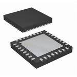
| 供应商器件封装 | 32-LFCSP-VQ(5x5) |
| 其它名称 | AD9945KCPZRL7DKR |
| 包装 | Digi-Reel® |
| 安装类型 | 表面贴装 |
| 封装/外壳 | 32-VFQFN 裸露焊盘,CSP |
| 接口 | 3 线串口 |
| 标准包装 | 1 |
| 电流-电源 | - |
| 类型 | CCD 信号处理器,12 位 |
| 输入类型 | 逻辑 |
| 输出类型 | 逻辑 |


- 商务部:美国ITC正式对集成电路等产品启动337调查
- 曝三星4nm工艺存在良率问题 高通将骁龙8 Gen1或转产台积电
- 太阳诱电将投资9.5亿元在常州建新厂生产MLCC 预计2023年完工
- 英特尔发布欧洲新工厂建设计划 深化IDM 2.0 战略
- 台积电先进制程称霸业界 有大客户加持明年业绩稳了
- 达到5530亿美元!SIA预计今年全球半导体销售额将创下新高
- 英特尔拟将自动驾驶子公司Mobileye上市 估值或超500亿美元
- 三星加码芯片和SET,合并消费电子和移动部门,撤换高东真等 CEO
- 三星电子宣布重大人事变动 还合并消费电子和移动部门
- 海关总署:前11个月进口集成电路产品价值2.52万亿元 增长14.8%


PDF Datasheet 数据手册内容提取
Complete 12-Bit 40 MHz CCD Signal Processor AD9945 FEATURES GENERAL DESCRIPTION 40 MSPS Correlated Double Sampler (CDS) The AD9945 is a complete analog signal processor for CCD 6 dB to 40 dB 10-Bit Variable Gain Amplifier (VGA) applications. It features a 40 MHz single-channel architecture Low Noise Optical Black Clamp Circuit designed to sample and condition the outputs of interlaced and Preblanking Function progressive scan area CCD arrays. The AD9945’s signal chain 12-Bit 40 MSPS A/D Converter consists of a correlated double sampler (CDS), a digitally con- No Missing Codes Guaranteed trolled variable gain amplifier (VGA), a black level clamp, and a 3-Wire Serial Digital Interface 12-bit A/D converter. 3 V Single-Supply Operation The internal registers are programmed through a 3-wire serial digital Low Power: 160 mW @ 3 V Supply interface. Programmable features include gain adjustment, black Space-Saving 32-Lead 5 mm (cid:2) 5 mm LFCSP level adjustment, input clock polarity, and power-down modes. APPLICATIONS The AD9945 operates from a single 3 V power supply, typi- Digital Still Cameras cally dissipates 160 mW, and is packaged in a space-saving Digital Video Camcorders 32-lead LFCSP. PC Cameras Portable CCD Imaging Devices CCTV Cameras FUNCTIONAL BLOCK DIAGRAM REFT REFB PBLK AD9945 BAND GAP DRVDD REFERENCE DRVSS 6dB TO 40dB 12 CCDIN CDS VGA 12-BIT DOUT ADC CLP AVDD 10 CLPOB AVSS CONTROL REGISTERS DVDD DIGITAL INTERNAL INTERFACE TIMING DVSS SL SCK SDATA SHP SHD DATACLK C REV. Information furnished by Analog Devices is believed to be accurate and reliable. However, no responsibility is assumed by Analog Devices for its use, nor for any infringements of patents or other rights of third parties that may result from its use. No license is granted by implication or otherwise One Technology Way, P.O. Box 9106, Norwood, MA 02062-9106, U.S.A. under any patent or patent rights of Analog Devices. Trademarks and Tel: 781/329-4700 www.analog.com registered trademarks are the property of their respective owners. Fax: 781/461-3113 ©2013 Analog Devices, Inc. All rights reserved.
AD9945–SPECIFICATIONS GENERAL SPECIFICATIONS (T to T , AVDD = DVDD = DRVDD= 3.0 V, f = 40 MHz, unless otherwise noted.) MIN MAX SAMP Parameter Min Typ Max Unit TEMPERATURE RANGE Operating –20 +85 °C Storage –65 +150 °C POWER SUPPLY VOLTAGE Analog, Digital, Digital Driver 2.85 3.6 V POWER CONSUMPTION Normal Operation (DRVDD Power not Included) 160 mW DRVDD Power Only (C = 20 pF) 10 mW LOAD Power-Down Mode 1.5 mW MAXIMUM CLOCK RATE 40 MHz Specifications subject to change without notice. DIGITAL SPECIFICATIONS (DRVDD=DVDD=2.85V,C =20pF,unlessotherwisenoted.) L Parameter Symbol Min Typ Max Unit LOGIC INPUTS High Level Input Voltage V 2.1 V IH Low Level Input Voltage V 0.6 V IL High Level Input Current I 10 μA IH Low Level Input Current I 10 μA IL Input Capacitance C 10 pF IN LOGIC OUTPUTS High Level Output Voltage, I = 2 mA V 2.2 V OH OH Low Level Output Voltage, I = 2 mA V 0.5 V OL OL Specifications subject to change without notice. –2– REV. C
AD9945 SYSTEM SPECIFICATIONS (T M I N to TMAX, AVDD = DVDD = DRVDD = 3.0 V, fS A M P = 40 MHz, Register 0xD = 0x838, unless otherwise noted.) Parameter Min Typ Max Unit Notes CDS Maximum Input Range before Saturation* 1.0 Vp-p Allowable CCD Reset Transient* 500 mV See Input Waveform in Footnote Maximum CCD Black Pixel Amplitude* 100 mV VARIABLE GAIN AMPLIFIER (VGA) Gain Control Resolution 1024 Steps Gain Monotonicity Guaranteed Gain Range Minimum Gain 5.3 dB SeeFigure7forVGAGainCurve Maximum Gain 40.0 41.5 dB SeeVariableGainAmplifiersectionforVGAgainequation LowGainMode (cid:166)1.5 0 +1.5 dB SeeTable1,InternalRegisterMap,forregisterinformation BLACK LEVEL CLAMP Clamp Level Resolution 256 Steps Clamp Level Measured at ADC Output Minimum Clamp Level 0 LSB Maximum Clamp Level 255 LSB A/D CONVERTER Resolution 12 Bits Differential Nonlinearity (DNL) ±0.5 LSB No Missing Codes Guaranteed Data Output Coding Straight Binary Full-Scale Input Voltage 2.0 V VOLTAGE REFERENCE Reference Top Voltage (REFT) 2.0 V Reference Bottom Voltage (REFB) 1.0 V SYSTEM PERFORMANCE Specifications Include Entire Signal Chain Gain Range Low Gain (VGA Code = 0) 5.3 dB Maximum Gain (VGA Code = 1023) 40.0 41.5 dB Gain Accuracy (cid:3)1.0 dB Peak Nonlinearity, 500 mV Input Signal 0.1 % 12 dB Gain Applied Total Output Noise 1.2 LSB rms AC Grounded Input, 6 dB Gain Applied Power Supply Rejection (PSR) 40 dB *Input Signal Characteristics defined as follows: 500mV TYP RESET TRANSIENT 100mV TYP OPTICAL BLACK PIXEL 1V TYP INPUT SIGNAL RANGE Specifications subject to change without notice. C REV. –3–
AD9945 TIMING SPECIFICATIONS (C = 20 pF, f = 40 MHz, CCD Mode Timing in Figures 8 and 9, Serial Timing in Figures 4 and 5.) L SAMP Parameter Symbol Min Typ Max Unit SAMPLE CLOCKS DATACLK, SHP, SHD Clock Period t 25 ns CONV DATACLK High/Low Pulse Width t 10 12.5 ns ADC SHP Pulse Width t 6.25 ns SHP SHD Pulse Width t 6.25 ns SHD CLPOB Pulse Width* t 2 20 Pixels COB SHP Rising Edge to SHD Falling Edge t 6.25 ns S1 SHP Rising Edge to SHD Rising Edge t 11.25 12.5 ns S2 Internal Clock Delay t 3 ns ID DATA OUTPUTS Output Delay t 9.5 ns OD Pipeline Delay 10 Cycles SERIAL INTERFACE Maximum SCK Frequency f 10 MHz SCLK SL to SCK Setup Time t 10 ns LS SCK to SL Hold Time t 10 ns LH SDATA Valid to SCK Rising Edge Setup t 10 ns DS SCK Falling Edge to SDATA Valid Hold t 10 ns DH *Minimum CLPOB pulse width is for functional operation only. Wider typical pulses are recommended to achieve low noise clamp performance. Specifications subject to change without notice. ABSOLUTE MAXIMUM RATINGS* With Respect Parameter To Min Max Unit AVDD AVSS –0.3 +3.9 V DVDD DVSS –0.3 +3.9 V DRVDD DRVSS –0.3 +3.9 V Digital Outputs DRVSS –0.3 DRVDD + 0.3 V SHP, SHD, DATACLK DVSS –0.3 DVDD + 0.3 V CLPOB, PBLK DVSS –0.3 DVDD + 0.3 V SCK, SL, SDATA DVSS –0.3 DVDD + 0.3 V REFT, REFB, CCDIN AVSS –0.3 AVDD + 0.3 V Junction Temperature 150 °C THERMAL CHARACTERISTICS Lead Temperature 300 °C Thermal Resistance 32-Lead LFCSP Package (10 sec) θ = 27.7 °C/W JA *Stresses above those listed under Absolute Maximum Ratings may cause perma- nent damage to the device. This is a stress rating only; functional operation of the device at these or any other conditions outside of those indicated in the operational sections of this specification is not implied. Exposure to absolute maximum ratings for extended periods may affect device reliability. CAUTION ESD (electrostatic discharge) sensitive device. Electrostatic charges as high as 4000 V readily accumulate on the human body and test equipment and can discharge without detection. Although the AD9945 features proprietary ESD protection circuitry, permanent damage may occur on devices subjected to high energy electrostatic discharges. Therefore, proper ESD precautions are recommended to avoid performance degradation or loss of functionality. C –4– REV.
AD9945 PIN CONFIGURATION A T KA 10CCCCDL DDNNNSSS 2 1 0 9 8 7 6 5 33322222 D2 1 PIN 1 24 REFB D3 2 INDICATOR 23 REFT D4 3 22 CCDIN D5 4 AD9945 21 AVSS D6 5 20 AVDD D7 6 TOP VIEW 19 SHD D8 7 18 SHP D9 8 17 CLPOB D10 9D11 10DRVDD 11DRVSS 12DVDD 13ATACLK 14DVSS 15PBLK 16 NOTES D 1. IT IS RECOMMENDED THAT THE EXPOSED PAD BE SOLDERED TO THE GROUND PLANE OF THE PCB. PIN FUNCTION DESCRIPTIONS Pin Number Mnemonic Type Description 1 to 10, 31, 32 D2 to D11, D0, D1 DO Digital Data Outputs 11 DRVDD P Digital Output Driver Supply 12 DRVSS P Digital Output Driver Ground 13 DVDD P Digital Supply 14 DATACLK DI Digital Data Output Latch Clock 15 DVSS P Digital Supply Ground 16 PBLK DI Preblanking Clock Input 17 CLPOB DI Black Level Clamp Clock Input 18 SHP DI CDS Sampling Clock for CCD’s Reference Level 19 SHD DI CDS Sampling Clock for CCD’s Data Level 20 AVDD P Analog Supply 21 AVSS P Analog Ground 22 CCDIN AI Analog Input for CCD Signal 23 REFT AO A/D Converter Top Reference Voltage Decoupling 24 REFB AO A/D Converter Bottom Reference Voltage Decoupling 25 SL DI Serial Digital Interface Load Pulse 26 SDATA DI Serial Digital Interface Data Input 27 SCK DI Serial Digital Interface Clock Input 28 to 30 NC NC Internally Pulled Down. Float or connect to GND. TYPE: AI = Analog Input, AO = Analog Output, DI = Digital Input, DO = Digital Output, P = Power. C REV. –5–
AD9945 DEFINITIONS OF SPECIFICATIONS at the specified gain setting. The output noise can be converted Differential Nonlinearity (DNL) to an equivalent voltage, using the relationship An ideal ADC exhibits code transitions that are exactly 1LSB 1 LSB = (ADC Full Scale/2N codes) apart. DNL is the deviation from this ideal value. Thus, every where N is the bit resolution of the ADC. For the AD9945, code must have a finite width. No missing codes guaranteed to 1 LSB is 0.5mV. 12-bit resolution indicates that all 4096 codes must be present over all operating conditions. Power Supply Rejection (PSR) The PSR is measured with a step change applied to the supply Peak Nonlinearity Peak nonlinearity, a full signal chain specification, refers to the pins. This represents a very high frequency disturbance on the peak deviation of the output of the AD9945 from a true straight AD9945’s power supply. The PSR specification is calculated line. The point used as zero scale occurs 1/2 LSB before the first from the change in the data outputs for a given step change in code transition. Positive full scale is defined as a level 11/2LSB the supply voltage. beyond the last code transition. The deviation is measured from Internal Delay for SHP/SHD the middle of each particular output code to the true straight line. The internal delay (also called aperture delay) is the delay that The error is then expressed as a percentage of the 2V ADC full- occurs from the time when a sampling edge is applied to the scale signal. The input signal is always appropriately gained up to AD9945 until the actual sample of the input signal is held. Both fill the ADC’s full-scale range. SHP and SHD sample the input signal during the transition from low to high, so the internal delay is measured from each clock’s Total Output Noise The rms output noise is measured using histogram techniques. rising edge to the instant the actual internal sample is taken. The standard deviation of the ADC output codes is calculated in LSB and represents the rms noise level of the total signal chain EQUIVALENT INPUT CIRCUITS DVDD AVDD 330(cid:4) 60(cid:4) DVSS AVSS AVSS Figure 1.Digital Inputs—SHP, SHD, Figure 3. CCDIN (Pin 22) DATACLK, CLPOB, PBLK, SCK, SL, SDATA DVDD DRVDD DATA THREE- DOUT STATE DVSS DRVSS Figure 2.Data Outputs—D0 to D11 C –6– REV.
Typical Performance Characteristics–AD9945 180 1.0 165 N (mV)150 VDD = 3.3 V 0.5 O SSIPATI135 VDD = 3.0 V L (LSB) 0 R DI DN E W120 O P – 0.5 105 90 – 1.0 25 32 40 0 800 1600 2400 3200 4000 SAMPLE RATE (MHz) CODE TPC 1.Power vs. Sampling Rate TPC 2.Typical DNL Performance C REV. –7–
AD9945 INTERNAL REGISTER DESCRIPTION Table I. Internal Register Map Register Address Bits Name A3 A2 A1 A0 Data Bits Function Operation 0 0 0 0 D0 Software Reset (0 = Normal Operation, 1 = Reset all registers to default) D2, D1 Power-Down Modes (00 = Normal Power, 01 = Standby, 10 = Total Shutdown) D3 OB Clamp Disable (0 = Clamp ON, 1 = Clamp OFF) D5, D4 Test Mode. Should always be set to 00. D6 PBLK Blanking Level (0 = Blank Output to Zero, 1 = Blank to OB Clamp Level) D8,D7 LowGainMode.Normallysetto00.Toenablelowgainmode,setto11.Whenlowgainmode isenabled,VGAGainregistermustbesettoallzeroes. D11toD9 TestMode.Shouldalwaysbesetto000. Control 0 0 0 1 D0 SHP/SHD Input Polarity (0 = Active Low, 1 = Active High) D1 DATACLK Input Polarity (0 = Active Low, 1 = Active High) D2 CLPOB Input Polarity (0 = Active Low, 1 = Active High) D3 PBLK Input Polarity (0 = Active Low, 1 = Active High) D4 Three-State Data Outputs (0 = Outputs Active, 1 = Outputs Three-Stated) D5 Data Output Latching (0 = Latched by DATACLK, 1 = Latch is Transparent) D6 Data Output Coding (0 = Binary Output, 1 = Gray Code Output) D11 to D7 Test Mode. Should always be set to 00000. Clamp Level 0 0 1 0 D7 to D0 OB Clamp Level (0 = 0 LSB, 255 = 255 LSB) VGA Gain 0 0 1 1 D9 to D0 VGA Gain (0 = 6 dB, 1023 = 40 dB) Startup 1 1 0 1 D11 to D0 Required start-up write must be set to 0x838. NOTE: All register values default to 0x0000 at power-up except clamp level, which defaults to 128 decimal (128 LSB clamp level). C –8– REV.
AD9945 SERIAL INTERFACE SDATA A0 A1 A2 A3 D0 D1 D2 D3 D4 D5 D6 D7 D8 D9 D10 D11 tDS tDH SCK t t LS LH SL NOTES 1. SDATA BITS ARE INTERNALLY LATCHED ON THE RISING EDGES OF SCK. 2. SYSTEM UPDATE OF LOADED REGISTERS OCCURS ON SL RISING EDGE. 3.ALL 12 DATA BITS D0 TO D11 MUST BE WRITTEN. IF THE REGISTER CONTAINS FEWER THAN 12 BITS, ZEROS SHOULD BE USED FOR THE UNDEFINED BITS. Figure 4.Serial Write Operation DATA FOR STARTING DATA FOR NEXT REGISTER ADDRESS REGISTER ADDRESS ... ... ... SDATA A0 A1 A2 A3 D0 D1 D2 D3 D4 D5 D10 D11 D0 D1 D10 D11 D0 D1 D2 ... ... ... SCK 1 2 3 4 5 6 7 8 9 10 15 16 17 18 27 28 29 30 31 ... ... ... SL NOTES 1. MULTIPLE SEQUENTIAL REGISTERS MAY BE LOADED CONTINUOUSLY. 2. THE FIRST (LOWEST ADDRESS) REGISTER ADDRESS IS WRITTEN, FOLLOWED BY MULTIPLE 12-BIT DATA-WORDS. 3. THE ADDRESS WILL AUTOMATICALLY INCREMENT WITH EACH 12-BIT DATA-WORD (ALL 12 BITS MUST BE WRITTEN). 4. SL IS HELD LOW UNTIL THE LAST DESIRED REGISTER HAS BEEN LOADED. 5. NEW DATA IS UPDATED AT THE NEXT SL RISING EDGE. Figure 5.Continuous Serial Write Operation to All Registers C REV. –9–
AD9945 DC RESTORE INTERNAL VREF 6dB TO 40dB 2V FULL SCALE 0.1(cid:5)F CCDIN 12-BIT 12 CDS VGA DOUT ADC 8-BIT OPTICAL BLACK CLPOB 10 DAC CLAMP DIGITAL FILTERING VGA GAIN REGISTER 8 CLAMP LEVEL REGISTER Figure 6.CCD Mode Block Diagram CIRCUIT DESCRIPTION AND OPERATION When the loop is disabled, the clamp level register may still be The AD9945 signal processing chain is shown in Figure 6. Each used to provide programmable offset adjustment. processing step is essential in achieving a high quality image from Horizontal timing is shown in Figure 9. The CLPOB pulse should the raw CCD pixel data. be placed during the CCD’s optical black pixels. It is recom- DC Restore mended that the CLPOB pulse be used during valid CCD dark To reduce the large dc offset of the CCD output signal, a dc pixels. The CLPOB pulse should be a minimum of 20 pixels wide restore circuit is used with an external 0.1μF series coupling to minimize clamp noise. Shorter pulse widths may be used, but capacitor. This restores the dc level of the CCD signal to clamp noise may increase and the loop’s ability to track low fre- approximately 1.5V to be compatible with the 3V single supply quency variations in the black level will be reduced. of the AD9945. A/D Converter Correlated Double Sampler The ADC uses a 2 V input range. Better noise performance results The CDS circuit samples each CCD pixel twice to extract the from using a larger ADC full-scale range. The ADC uses a video information and reject low frequency noise. The timing pipelined architecture with a 2 V full-scale input for low noise shown in Figure8 illustrates how the two CDS clocks, SHP and performance. SHD, are used to sample the reference level and data level of Variable Gain Amplifier the CCD signal, respectively. The CCD signal is sampled on the The VGA stage provides a gain range of 6 dB to 40 dB, program- rising edges of SHP and SHD. Placement of these two clock mable with 10-bit resolution through the serial digital interface. signals is critical in achieving the best performance from the CCD. The minimum gain of 6 dB is needed to match a 1 V input signal An internal SHP/SHD delay (t ) of 3 ns is caused by internal ID with the ADC full-scale range of 2 V. A plot of the VGA gain curve propagation delays. is shown in Figure 7. Optical Black Clamp VGAGain(dB)=(VGACode×0.035dB)+5.3dB The optical black clamp loop is used to remove residual offsets in the signal chain and to track low frequency variations in the 42 CCD’s black level. During the optical black (shielded) pixel interval on each line, the ADC output is compared with the fixed black level reference, selected by the user in the clamp 36 level register. The resulting error signal is filtered to reduce noise, and the correction value is applied to the ADC input 30 B) through a D/A converter. Normally, the optical black clamp d loop is turned on once per horizontal line, but this loop can be AIN ( 24 G updated more slowly to suit a particular application. If external A G digital clamping is used during the postprocessing, the AD9945 V 18 optical black clamping may be disabled using Bit D3 in the operation register (see the Serial Interface Timing and Internal 12 Register Description sections). 6 0 127 255 383 511 639 767 895 1023 VGA GAIN REGISTER CODE Figure 7.VGA Gain Curve C –10– REV.
AD9945 CCD MODE TIMING CCD SIGNAL N N+1 N+2 N+9 N+10 t ID t ID SHP tS1 tS2 tCP SHD DATACLK t OD OUTPUT N–10 N–9 N–8 N–1 N DATA NOTES 1. RECOMMENDED PLACEMENT FOR DATACLK RISING EDGE IS BETWEEN THE SHD RISING EDGE AND NEXT SHP FALLING EDGE. 2. CCD SIGNAL IS SAMPLED AT SHP AND SHD RISING EDGES. Figure 8.CCD Mode Timing HORIZONTAL EFFECTIVE PIXELS OPTICAL BLACK PIXELS BLANKING DUMMY PIXELS EFFECTIVE PIXELS CCD SIGNAL CLPOB PBLK OUTPUT DATA EFFECTIVE PIXEL DATA OB PIXEL DATA DUMMY BLACK EFFECTIVE DATA NOTES 1. CLPOB WILL OVERWRITE PBLK. PBLK WILL NOT AFFECT CLAMP OPERATION IF OVERLAPPING WITH CLPOB. 2. PBLK SIGNAL IS OPTIONAL. 3. DIGITAL OUTPUT DATA WILL BE ALL ZEROS DURING PBLK. OUTPUT DATA LATENCY IS NINE DATACLK CYCLES. Figure 9.Typical CCD Mode Line Clamp Timing C REV. –11–
AD9945 APPLICATIONS INFORMATION level correction, and analog-to-digital conversion. The AD9945’s The AD9945 is a complete analog front end (AFE) product for digital output data is then processed by the image processing digital still camera and camcorder applications. As shown in ASIC. The internal registers of the AD9945—used to control Figure10, the CCD image (pixel) data is buffered and sent to the gain, offset level, and other functions—are programmed by the AD9945 analog input through a series input capacitor. The ASIC or microprocessor through a 3-wire serial digital interface. AD9945 performs the dc restoration, CDS, gain adjustment, black A system timing generator provides the clock signals for both the CCD and the AFE. CCD AD9945 DIGITAL VOUT 0.1(cid:5)F ADCOUT OUTPUTS DIGITAL IMAGE CCDIN SERIAL PROCESSING REGISTER- INTERFACE ASIC DATA BUFFER CDS/CLAMP V-DRIVE TIMING CCD TIMING TIMING GENERATOR Figure 10.System Applications Diagram C –12– REV.
AD9945 Internal Power-On Reset Circuitry provide the lowest possible impedance path between the power After power-on, the AD9945 will automatically reset all internal and bypass pins and their respective ground pins. All decoupling registers and perform internal calibration procedures. This takes capacitors should be located as close as possible to the package approximately 1 ms to complete. During this time, normal clock pins. A single clean power supply is recommended for the AD9945, signals and serial write operations may occur. However, serial but a separate digital driver supply may be used for DRVDD register writes will be ignored until the internal reset operation (Pin 11). DRVDD should always be decoupled to DRVSS (Pin 12), is completed. which should be connected to the analog ground plane. If the digital outputs (Pins 1 to 10, 31, and 32) must drive a load larger than 20 pF, Required Start-Up Write During power-up of the AD9945, 0x838 must be written into buffering is recommended to reduce digital code transition noise. Register 0xD for proper start-up operation. Alternatively, placing series resistors close to the digital output pins may also help reduce noise. Grounding and Decoupling Recommendations As shown in Figure 11, a single ground plane is recommended for the AD9945. This ground plane should be as continuous as possible. This will ensure that all analog decoupling capacitors SERIAL 3 INTERFACE A D0 T K A D1 NC NC NC SC SD SL 2 1 0 9 8 7 6 5 3 3 3 2 2 2 2 2 D2 1 24 REFB 1.0(cid:5)F PIN 1 D3 2 IDENTIFIER 23 REFT 1.0(cid:5)F 0.1(cid:5)F D4 3 22 CCDIN CCDIN D5 4 21 AVSS AD9945 D6 5 20 AVDD 3V ANALOG D7 6 19 SHD SUPPLY D8 7 TOP VIEW 18 SHP 0.1(cid:5)F (Not to Scale) D9 8 17 CLPOB 0 9 101 11D 12S 13D K14 15S 16K D1 D1 VD VS VD CL VS BL R R D A D P D D T A D DATA 12 5 CLOCK OUTPUTS INPUTS 3V 3V DRIVER ANALOG SUPPLY SUPPLY 0.1(cid:5)F 0.1(cid:5)F NC = NO CONNECT NOTE THE EXPOSED PAD ON THE BOTTOM OF THE AD9945 SHOULD BE SOLDERED TO THE GND PLANE OF THE PRINTED CIRCUIT BOARD Figure 11.Recommended Circuit Configuration for CCD Mode C REV. –13–
AD9945 OUTLINE DIMENSIONS 5.10 0.30 5.00 SQ 0.25 PIN 1 4.90 0.18 INDICATOR PIN1 25 32 INDICATOR 24 1 0.50 BSC EXPOSED 3.25 PAD 3.10 SQ 2.95 17 8 0.50 16 9 0.25 MIN TOP VIEW 0.40 BOTTOM VIEW 0.30 FOR PROPER CONNECTION OF 0.80 THE EXPOSED PAD, REFER TO 0.75 THE PIN CONFIGURATION AND 0.05 MAX FUNCTION DESCRIPTIONS 0.70 0.02 NOM SECTION OF THIS DATA SHEET. COPLANARITY 0.08 SEATING 0.20 REF PLANE COMPLIANT TO JEDEC STANDARDS MO-220-WHHD. 112408-A Figure 12. 32-Lead Lead Frame Chip Scale Package [LFCSP_WQ] 5 mm × 5 mm Body, Very Very Thin Quad (CP-32-7) Dimensions shown in millimeters ORDERING GUIDE Model1 Temperature Range Package Description Package Option AD9945KCPZ −20°C to +85°C 32-Lead Lead Frame Chip Scale Package [LFCSP_WQ] CP-32-7 AD9945KCPZRL7 −20°C to +85°C 32-Lead Lead Frame Chip Scale Package [LFCSP_WQ] CP-32-7 1 Z = RoHS Compliant Part. REVISION HISTORY 5/13—Rev. B to Rev. C Changes to TPC 1 .............................................................................. 7 Changes to Table 1 ............................................................................ 8 Updated Outline Dimensions ........................................................ 14 Changes to Figure 4 and Figure 5 ................................................... 9 Changes to Ordering Guide ........................................................... 14 Added Required Start-Up Write Section ..................................... 13 1/11—Rev. A to Rev. B Changes to Grounding and Decoupling Recommendations Changed 140 mW to 160 mW Throughout .................................. 1 Section .............................................................................................. 13 Changes to Power Supply Voltage Parameter and Power Moved Ordering Guide .................................................................. 14 Consumption, Normal Operation (DRVDD Power not Changes to Ordering Guide ........................................................... 14 Included) Parameter in General Specifications Table .................. 2 11/03—Rev. 0 to Rev. A Changed 2.7 V to 2.85 V in Digital Specifications Table Changes to Timing Specifications................................................... 4 Summary ............................................................................................ 2 Changes to Ordering Guide ............................................................. 4 Changes to System Specifications Table Summary ....................... 3 Changes to Figure 11 ...................................................................... 13 Added Low Gain Mode Parameter in System Specifications Updated Outline Dimensions ........................................................ 14 Table .................................................................................................... 3 Added Exposed Pad Notation to Pin Configuration .................... 5 ©2013 Analog Devices, Inc. All rights reserved. Trademarks and registered trademarks are the property of their respective owners. D03636-0-5/13(C) Rev. C | Page 14 of 14