ICGOO在线商城 > 集成电路(IC) > 嵌入式 - FPGA(现场可编程门阵列) > XC7A100T-3CSG324E
 Datasheet下载
- 型号: XC7A100T-3CSG324E
- 制造商: Xilinx
- 库位|库存: xxxx|xxxx
- 要求:
| 数量阶梯 | 香港交货 | 国内含税 |
| +xxxx | $xxxx | ¥xxxx |
查看当月历史价格
查看今年历史价格
XC7A100T-3CSG324E产品简介:
ICGOO电子元器件商城为您提供XC7A100T-3CSG324E由Xilinx设计生产,在icgoo商城现货销售,并且可以通过原厂、代理商等渠道进行代购。 XC7A100T-3CSG324E价格参考¥1691.25-¥1691.25。XilinxXC7A100T-3CSG324E封装/规格:嵌入式 - FPGA(现场可编程门阵列), 。您可以下载XC7A100T-3CSG324E参考资料、Datasheet数据手册功能说明书,资料中有XC7A100T-3CSG324E 详细功能的应用电路图电压和使用方法及教程。
Xilinx Inc.(赛灵思)的XC7A100T-3CSG324E属于Artix-7系列FPGA,是一款低功耗、高性能的嵌入式现场可编程门阵列。该型号具有丰富的逻辑资源、数字信号处理能力以及高速接口支持,适用于多种应用场景。以下是其主要应用领域及特点:

 1. 工业自动化与控制
   - XC7A100T可用于工业自动化中的实时控制和数据采集系统。
   - 提供高精度的时序控制和并行处理能力,适合复杂的运动控制和机器人应用。
   - 支持多种通信协议(如EtherCAT、PROFINET等),便于构建分布式控制系统。

 2. 通信设备
   - 在无线通信中,用于基带信号处理、调制解调器设计以及协议栈实现。
   - 可作为小型基站或远程射频单元的核心处理器。
   - 具备灵活的接口配置,支持多种通信标准。

 3. 医疗成像
   - 应用于超声波、CT扫描仪和其他医学成像设备中。
   - 提供图像处理加速功能,例如滤波、增强和压缩。
   - 实现低延迟的数据传输和处理,满足医疗设备对实时性的要求。

 4. 视频与图像处理
   - 支持高清和4K视频流的编码、解码和后处理。
   - 提供灵活的接口选项(如MIPI、LVDS),适配摄像头模组和显示面板。
   - 广泛应用于安防监控、无人机视觉和虚拟现实设备。

 5. 汽车电子
   - 用于高级驾驶辅助系统(ADAS)、传感器融合和车载信息娱乐系统。
   - 提供强大的数据处理能力和低功耗特性,满足汽车环境的需求。
   - 支持ISO 26262等功能安全标准(需结合额外设计流程)。

 6. 航空航天与国防
   - 在雷达、卫星通信和导航系统中发挥重要作用。
   - 提供抗辐射选型(如Q-grade器件),适用于严苛的工作环境。
   - 支持复杂算法的硬件加速,提升系统性能。

 7. 边缘计算与物联网
   - 作为边缘端的智能节点,执行数据预处理和本地决策。
   - 集成多种传感器接口,支持多协议通信。
   - 提供高效的能耗比,延长电池供电设备的续航时间。

 总结
XC7A100T-3CSG324E凭借其丰富的资源、低功耗特性和高度灵活性,成为嵌入式系统开发的理想选择。无论是工业控制、通信设备还是消费电子产品,这款FPGA都能为开发者提供强大的硬件平台支持,同时缩短产品上市时间。
| 参数 | 数值 |
| 产品目录 | 集成电路 (IC) |
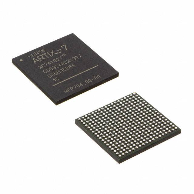
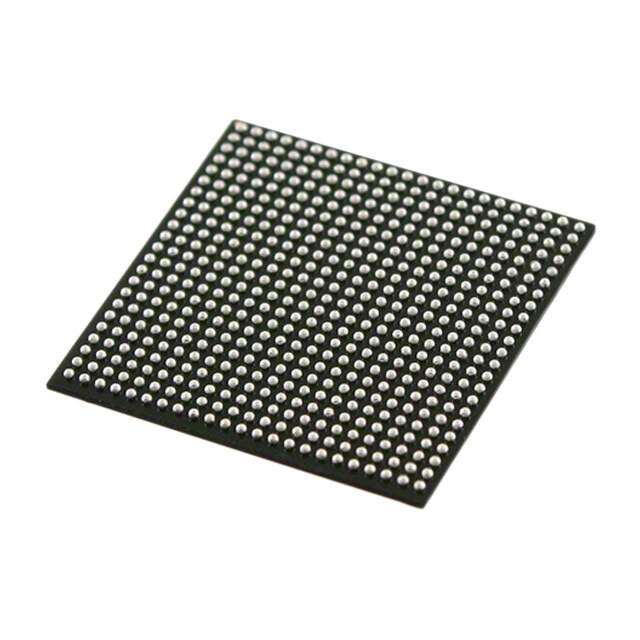
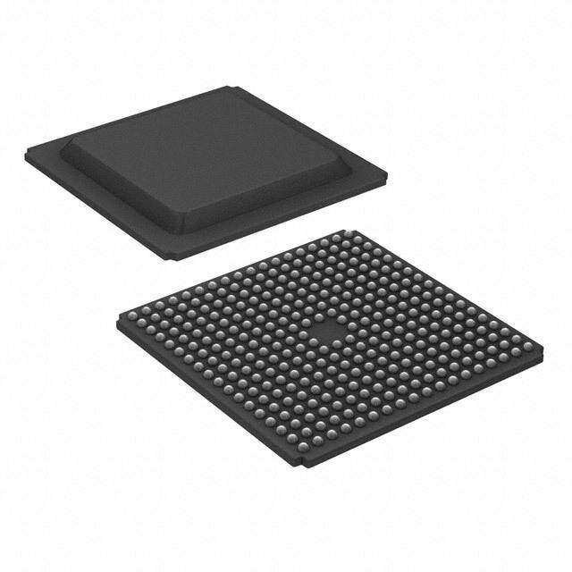
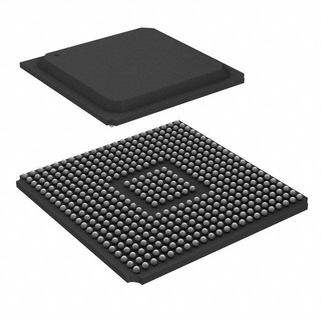
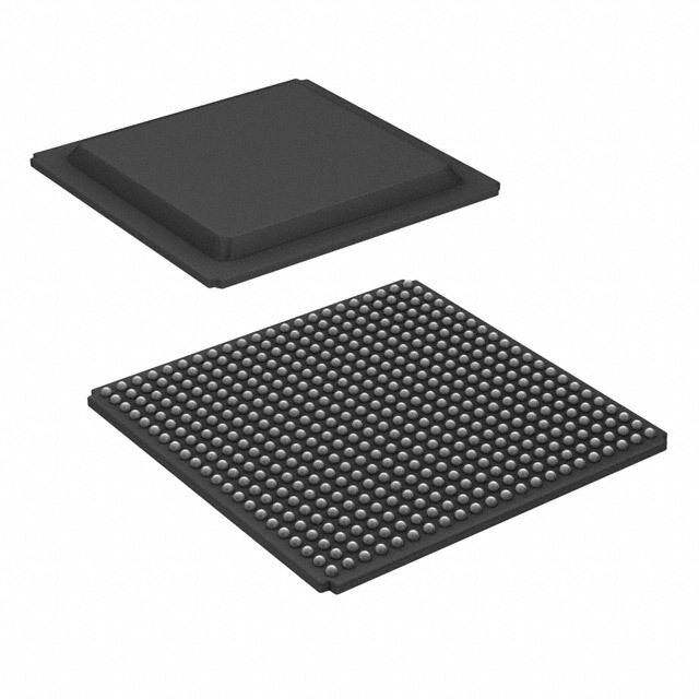
| 描述 | IC FPGA 210 I/O 324CSBGA |
| 产品分类 | |
| I/O数 | 210 |
| LAB/CLB数 | 7925 |
| 品牌 | Xilinx Inc |
| 数据手册 | 点击此处下载产品Datasheet点击此处下载产品Datasheet点击此处下载产品Datasheet点击此处下载产品Datasheet |
| 产品图片 |
|
| 产品型号 | XC7A100T-3CSG324E |
| PCN组件/产地 | |
| PCN设计/规格 | |
| rohs | 无铅 / 符合限制有害物质指令(RoHS)规范要求 |
| 产品系列 | Artix-7 |
| 产品培训模块 | http://www.digikey.cn/PTM/IndividualPTM.page?site=cn&lang=zhs&ptm=30320 |
| 供应商器件封装 | 324-CSPBGA (15x15) |
| 其它名称 | 122-1875 |
| 安装类型 | 表面贴装 |
| 封装/外壳 | 324-LFBGA,CSPBGA |
| 工作温度 | 0°C ~ 100°C |
| 总RAM位数 | 4976640 |
| 栅极数 | - |
| 标准包装 | 126 |
| 电压-电源 | 0.95 V ~ 1.05 V |
| 逻辑元件/单元数 | 101440 |


- 商务部:美国ITC正式对集成电路等产品启动337调查
- 曝三星4nm工艺存在良率问题 高通将骁龙8 Gen1或转产台积电
- 太阳诱电将投资9.5亿元在常州建新厂生产MLCC 预计2023年完工
- 英特尔发布欧洲新工厂建设计划 深化IDM 2.0 战略
- 台积电先进制程称霸业界 有大客户加持明年业绩稳了
- 达到5530亿美元!SIA预计今年全球半导体销售额将创下新高
- 英特尔拟将自动驾驶子公司Mobileye上市 估值或超500亿美元
- 三星加码芯片和SET,合并消费电子和移动部门,撤换高东真等 CEO
- 三星电子宣布重大人事变动 还合并消费电子和移动部门
- 海关总署:前11个月进口集成电路产品价值2.52万亿元 增长14.8%

PDF Datasheet 数据手册内容提取
Artix-7 FPGAs Data Sheet: DC and AC Switching Characteristics DS181 (v1.25) June 18, 2018 Product Specification Introduction Artix®-7 FPGAs are available in -3, -2, -1, -1LI, and -2L speed grade military device are the same as for a -1C speed speed grades, with -3 having the highest performance. The grade commercial device). However, only selected speed Artix-7FPGAs predominantly operate at a 1.0V core voltage. grades and/or devices are available in each temperature The -1LI and -2L devices are screened for lower maximum range. For example, -1M is only available in the static power and can operate at lower core voltages for defense-grade Artix-7Q family and -1Q is only available in lower dynamic power than the -1 and -2 devices, XAArtix-7FPGAs. respectively. The -1LI devices operate only at All supply voltage and junction temperature specifications V =V =0.95V and have the same speed CCINT CCBRAM are representative of worst-case conditions. The parameters specifications as the -1 speed grade. The -2L devices can included are common to popular designs and typical operate at either of two V voltages, 0.9V and 1.0V and CCINT applications. are screened for lower maximum static power. When operated at V =1.0V, the speed specification of a -2L Available device and package combinations can be found in: CCINT device is the same as the -2 speed grade. When operated at • 7Series FPGAs Overview (DS180) V =0.9V, the -2L static and dynamic power is reduced. CCINT • Defense-Grade 7Series FPGAs Overview (DS185) Artix-7 FPGA DC and AC characteristics are specified in • XA Artix-7 FPGAs Overview (DS197) commercial, extended, industrial, expanded (-1Q), and military (-1M) temperature ranges. Except the operating This Artix-7 FPGA data sheet, part of an overall set of temperature range or unless otherwise noted, all the DC documentation on the 7series FPGAs, is available on the and AC electrical parameters are the same for a particular Xilinx website at www.xilinx.com/documentation. speed grade (that is, the timing characteristics of a -1M DC Characteristics Table 1: Absolute Maximum Ratings(1) Symbol Description Min Max Units FPGA Logic V Internal supply voltage –0.5 1.1 V CCINT V Auxiliary supply voltage –0.5 2.0 V CCAUX V Supply voltage for the block RAM memories –0.5 1.1 V CCBRAM V Output drivers supply voltage for HR I/O banks –0.5 3.6 V CCO V Input reference voltage –0.5 2.0 V REF I/O input voltage –0.4 V +0.55 V CCO VIN(2)(3)(4) I/O input voltage (when VCCO=3.3V) for VREF and differential I/O standards –0.4 2.625 V except TMDS_33(5) V Key memory battery backup supply –0.5 2.0 V CCBATT GTP Transceiver V Analog supply voltage for the GTP transmitter and receiver circuits –0.5 1.1 V MGTAVCC V Analog supply voltage for the GTP transmitter and receiver termination circuits –0.5 1.32 V MGTAVTT V Reference clock absolute input voltage –0.5 1.32 V MGTREFCLK V Receiver (RXP/RXN) and Transmitter (TXP/TXN) absolute input voltage –0.5 1.26 V IN © 2011– 2018 Xilinx, Inc. XILINX, the Xilinx logo, Artix, Virtex, Kintex, Zynq, Spartan, ISE, Vivado and other designated brands included herein are trademarks of Xilinx in the United States and other countries. All other trademarks are the property of their respective owners. DS181 (v1.25) June 18, 2018 www.xilinx.com Send Feedback Product Specification 1
Artix-7 FPGAs Data Sheet: DC and AC Switching Characteristics Table 1: Absolute Maximum Ratings(1) (Cont’d) Symbol Description Min Max Units I DC input current for receiver input pins DC coupled RX termination=floating – 14 mA DCIN-FLOAT I DC input current for receiver input pins DC coupled RX termination=V – 12 mA DCIN-MGTAVTT MGTAVTT I DC input current for receiver input pins DC coupled RX termination=GND – 6.5 mA DCIN-GND I DC output current for transmitter pins DC coupled RX termination=floating – 14 mA DCOUT-FLOAT I DC output current for transmitter pins DC coupled RX termination=V – 12 mA DCOUT-MGTAVTT MGTAVTT XADC V XADC supply relative to GNDADC –0.5 2.0 V CCADC V XADC reference input relative to GNDADC –0.5 2.0 V REFP Temperature T Storage temperature (ambient) –65 150 °C STG Maximum soldering temperature for Pb/Sn component bodies(6) – +220 °C T SOL Maximum soldering temperature for Pb-free component bodies(6) – +260 °C T Maximum junction temperature(6) – +125 °C j Notes: 1. Stresses beyond those listed under Absolute Maximum Ratings might cause permanent damage to the device. These are stress ratings only, and functional operation of the device at these or any other conditions beyond those listed under Operating Conditions is not implied. Exposure to Absolute Maximum Ratings conditions for extended periods of time might affect device reliability. 2. The lower absolute voltage specification always applies. 3. For I/O operation, refer to 7Series FPGAs SelectIO Resources User Guide (UG471). 4. The maximum limit applies to DC signals. For maximum undershoot and overshoot AC specifications, see Table4. 5. See Table9 for TMDS_33 specifications. 6. For soldering guidelines and thermal considerations, see 7Series FPGA Packaging and Pinout Specification (UG475). Table 2: Recommended Operating Conditions(1)(2) Symbol Description Min Typ Max Units FPGA Logic For -3, -2, -2LE (1.0V), -1, -1Q, -1M devices: internal supply voltage 0.95 1.00 1.05 V V (3) For -1LI (0.95V) devices: internal supply voltage 0.92 0.95 0.98 V CCINT For -2LE (0.9V) devices: internal supply voltage 0.87 0.90 0.93 V V Auxiliary supply voltage 1.71 1.80 1.89 V CCAUX For -3, -2, -2LE (1.0V), -2LE (0.9V), -1, -1Q, -1M devices: block RAM supply 0.95 1.00 1.05 V V (3) voltage CCBRAM For -1LI (0.95V) devices: blockRAM supply voltage 0.92 0.95 0.98 V V (4)(5) Supply voltage for HR I/O banks 1.14 – 3.465 V CCO I/O input voltage –0.20 – V +0.20 V CCO VIN(6) I/O input voltage (when VCCO=3.3V) for VREF and differential I/O standards –0.20 – 2.625 V except TMDS_33(7) Maximum current through any pin in a powered or unpowered bank when – – 10 mA I (8) IN forward biasing the clamp diode. V (9) Battery voltage 1.0 – 1.89 V CCBATT GTP Transceiver V (10) Analog supply voltage for the GTP transmitter and receiver circuits 0.97 1.0 1.03 V MGTAVCC V (10) Analog supply voltage for the GTP transmitter and receiver termination circuits 1.17 1.2 1.23 V MGTAVTT XADC V XADC supply relative to GNDADC 1.71 1.80 1.89 V CCADC DS181 (v1.25) June 18, 2018 www.xilinx.com Send Feedback Product Specification 2
Artix-7 FPGAs Data Sheet: DC and AC Switching Characteristics Table 2: Recommended Operating Conditions(1)(2) (Cont’d) Symbol Description Min Typ Max Units V Externally supplied reference voltage 1.20 1.25 1.30 V REFP Temperature Junction temperature operating range for commercial (C) temperature devices 0 – 85 °C Junction temperature operating range for extended (E) temperature devices 0 – 100 °C T Junction temperature operating range for industrial (I) temperature devices –40 – 100 °C j Junction temperature operating range for expanded (Q) temperature devices –40 – 125 °C Junction temperature operating range for military (M) temperature devices –55 – 125 °C Notes: 1. All voltages are relative to ground. 2. For the design of the power distribution system consult 7 Series FPGAs PCB Design and Pin Planning Guide (UG483). 3. If V and V are operating at the same voltage, V and V should be connected to the same supply. CCINT CCBRAM CCINT CCBRAM 4. Configuration data is retained even if V drops to 0V. CCO 5. Includes V of 1.2V, 1.35V, 1.5V, 1.8V, 2.5V, and 3.3V at ±5%. CCO 6. The lower absolute voltage specification always applies. 7. See Table9 for TMDS_33 specifications. 8. A total of 200mA per bank should not be exceeded. 9. V is required only when using bitstream encryption. If battery is not used, connect V to either ground or V . CCBATT CCBATT CCAUX 10. Each voltage listed requires the filter circuit described in 7Series FPGAs GTP Transceiver User Guide (UG482). Table 3: DC Characteristics Over Recommended Operating Conditions Symbol Description Min Typ(1) Max Units V Data retention V voltage (below which configuration data might be lost) 0.75 – – V DRINT CCINT V Data retention V voltage (below which configuration data might be lost) 1.5 – – V DRI CCAUX I V leakage current per pin – – 15 µA REF REF I Input or output leakage current per pin (sample-tested) – – 15 µA L C (2) Die input capacitance at the pad – – 8 pF IN Pad pull-up (when selected) @ V =0V, V =3.3V 90 – 330 µA IN CCO Pad pull-up (when selected) @ V =0V, V =2.5V 68 – 250 µA IN CCO I Pad pull-up (when selected) @ V =0V, V =1.8V 34 – 220 µA RPU IN CCO Pad pull-up (when selected) @ V =0V, V =1.5V 23 – 150 µA IN CCO Pad pull-up (when selected) @ V =0V, V =1.2V 12 – 120 µA IN CCO I Pad pull-down (when selected) @ V =3.3V 68 – 330 µA RPD IN I Analog supply current, analog circuits in powered up state – – 25 mA CCADC I (3) Battery supply current – – 150 nA BATT Thevenin equivalent resistance of programmable input termination to V /2 28 40 55 Ω CCO (UNTUNED_SPLIT_40) Thevenin equivalent resistance of programmable input termination to V /2 35 50 65 Ω R (4) CCO IN_TERM (UNTUNED_SPLIT_50) Thevenin equivalent resistance of programmable input termination to V /2 44 60 83 Ω CCO (UNTUNED_SPLIT_60) DS181 (v1.25) June 18, 2018 www.xilinx.com Send Feedback Product Specification 3
Artix-7 FPGAs Data Sheet: DC and AC Switching Characteristics Table 3: DC Characteristics Over Recommended Operating Conditions (Cont’d) Symbol Description Min Typ(1) Max Units n Temperature diode ideality factor – 1.010 – – r Temperature diode series resistance – 2 – Ω Notes: 1. Typical values are specified at nominal voltage, 25°C. 2. This measurement represents the die capacitance at the pad, not including the package. 3. Maximum value specified for worst case process at 25°C. 4. Termination resistance to a V /2 level. CCO Table 4: V Maximum Allowed AC Voltage Overshoot and Undershoot for HR I/O Banks(1)(2) IN AC Voltage Overshoot % of UI @–55°C to 125°C AC Voltage Undershoot % of UI @–55°C to 125°C –0.40 100 –0.45 61.7 V +0.55 100 CCO –0.50 25.8 –0.55 11.0 V +0.60 46.6 –0.60 4.77 CCO V +0.65 21.2 –0.65 2.10 CCO V +0.70 9.75 –0.70 0.94 CCO V +0.75 4.55 –0.75 0.43 CCO V +0.80 2.15 –0.80 0.20 CCO V +0.85 1.02 –0.85 0.09 CCO V +0.90 0.49 –0.90 0.04 CCO V +0.95 0.24 –0.95 0.02 CCO Notes: 1. A total of 200mA per bank should not be exceeded. 2. The peak voltage of the overshoot or undershoot, and the duration above V +0.20V or below GND–0.20V, must not exceed the values CCO in this table. DS181 (v1.25) June 18, 2018 www.xilinx.com Send Feedback Product Specification 4
Artix-7 FPGAs Data Sheet: DC and AC Switching Characteristics Table 5: Typical Quiescent Supply Current Speed Grade Symbol Description Device 1.0V 0.95V 0.9V Units -3 -2 -2LE -1 -1LI -2LE I Quiescent V supply current XC7A12T 48 48 48 48 43 38 mA CCINTQ CCINT XC7A15T 95 95 95 95 58 66 mA XC7A25T 48 48 48 48 43 38 mA XC7A35T 95 95 95 95 58 66 mA XC7A50T 95 95 95 95 58 66 mA XC7A75T 155 155 155 155 96 108 mA XC7A100T 155 155 155 155 96 108 mA XC7A200T 328 328 328 328 203 232 mA XA7A12T N/A 48 N/A 48 N/A N/A mA XA7A15T N/A 95 N/A 95 N/A N/A mA XA7A25T N/A 48 N/A 48 N/A N/A mA XA7A35T N/A 95 N/A 95 N/A N/A mA XA7A50T N/A 95 N/A 95 N/A N/A mA XA7A75T N/A 155 N/A 155 N/A N/A mA XA7A100T N/A 155 N/A 155 N/A N/A mA XQ7A50T N/A 95 N/A 95 58 N/A mA XQ7A100T N/A 155 N/A 155 96 N/A mA XQ7A200T N/A 328 N/A 328 203 N/A mA I Quiescent V supply current XC7A12T 1 1 1 1 1 1 mA CCOQ CCO XC7A15T 1 1 1 1 1 1 mA XC7A25T 1 1 1 1 1 1 mA XC7A35T 1 1 1 1 1 1 mA XC7A50T 1 1 1 1 1 1 mA XC7A75T 4 4 4 4 4 4 mA XC7A100T 4 4 4 4 4 4 mA XC7A200T 5 5 5 5 5 5 mA XA7A12T N/A 1 N/A 1 N/A N/A mA XA7A15T N/A 1 N/A 1 N/A N/A mA XA7A25T N/A 1 N/A 1 N/A N/A mA XA7A35T N/A 1 N/A 1 N/A N/A mA XA7A50T N/A 1 N/A 1 N/A N/A mA XA7A75T N/A 4 N/A 4 N/A N/A mA XA7A100T N/A 4 N/A 4 N/A N/A mA XQ7A50T N/A 1 N/A 1 1 N/A mA XQ7A100T N/A 4 N/A 4 4 N/A mA XQ7A200T N/A 5 N/A 5 5 N/A mA DS181 (v1.25) June 18, 2018 www.xilinx.com Send Feedback Product Specification 5
Artix-7 FPGAs Data Sheet: DC and AC Switching Characteristics Table 5: Typical Quiescent Supply Current (Cont’d) Speed Grade Symbol Description Device 1.0V 0.95V 0.9V Units -3 -2 -2LE -1 -1LI -2LE I Quiescent V supply current XC7A12T 13 13 13 13 13 13 mA CCAUXQ CCAUX XC7A15T 22 22 22 22 19 22 mA XC7A25T 13 13 13 13 13 13 mA XC7A35T 22 22 22 22 19 22 mA XC7A50T 22 22 22 22 19 22 mA XC7A75T 36 36 36 36 32 36 mA XC7A100T 36 36 36 36 32 36 mA XC7A200T 73 73 73 73 65 73 mA XA7A12T N/A 13 N/A 13 N/A N/A mA XA7A15T N/A 22 N/A 22 N/A N/A mA XA7A25T N/A 13 N/A 13 N/A N/A mA XA7A35T N/A 22 N/A 22 N/A N/A mA XA7A50T N/A 22 N/A 22 N/A N/A mA XA7A75T N/A 36 N/A 36 N/A N/A mA XA7A100T N/A 36 N/A 36 N/A N/A mA XQ7A50T N/A 22 N/A 22 19 N/A mA XQ7A100T N/A 36 N/A 36 32 N/A mA XQ7A200T N/A 73 N/A 73 65 N/A mA DS181 (v1.25) June 18, 2018 www.xilinx.com Send Feedback Product Specification 6
Artix-7 FPGAs Data Sheet: DC and AC Switching Characteristics Table 5: Typical Quiescent Supply Current (Cont’d) Speed Grade Symbol Description Device 1.0V 0.95V 0.9V Units -3 -2 -2LE -1 -1LI -2LE I Quiescent V supply current XC7A12T 1 1 1 1 1 1 mA CCBRAMQ CCBRAM XC7A15T 2 2 2 2 1 2 mA XC7A25T 1 1 1 1 1 1 mA XC7A35T 2 2 2 2 1 2 mA XC7A50T 2 2 2 2 1 2 mA XC7A75T 4 4 4 4 2 4 mA XC7A100T 4 4 4 4 2 4 mA XC7A200T 11 11 11 11 6 11 mA XA7A12T N/A 1 N/A 1 N/A N/A mA XA7A15T N/A 2 N/A 2 N/A N/A mA XA7A25T N/A 1 N/A 1 N/A N/A mA XA7A35T N/A 2 N/A 2 N/A N/A mA XA7A50T N/A 2 N/A 2 N/A N/A mA XA7A75T N/A 4 N/A 4 N/A N/A mA XA7A100T N/A 4 N/A 4 N/A N/A mA XQ7A50T N/A 2 N/A 2 1 N/A mA XQ7A100T N/A 4 N/A 4 2 N/A mA XQ7A200T N/A 11 N/A 11 6 N/A mA Notes: 1. Typical values are specified at nominal voltage, 85°C junction temperature (T) with single-ended SelectIO resources. j 2. Typical values are for blank configured devices with no output current loads, no active input pull-up resistors, all I/O pins are 3-state and floating. 3. Use the Xilinx Power Estimator (XPE) spreadsheet tool (download at http://www.xilinx.com/power) to estimate static power consumption for conditions other than those specified. DS181 (v1.25) June 18, 2018 www.xilinx.com Send Feedback Product Specification 7
Artix-7 FPGAs Data Sheet: DC and AC Switching Characteristics Power-On/Off Power Supply Sequencing The recommended power-on sequence is V , V , V , and V to achieve minimum current draw and ensure CCINT CCBRAM CCAUX CCO that the I/Os are 3-stated at power-on. The recommended power-off sequence is the reverse of the power-on sequence. If V and V have the same recommended voltage levels then both can be powered by the same supply and ramped CCINT CCBRAM simultaneously. If V and V have the same recommended voltage levels then both can be powered by the same CCAUX CCO supply and ramped simultaneously. For V voltages of 3.3V in HR I/O banks and configuration bank 0: CCO • The voltage difference between V and V must not exceed 2.625V for longer than T for each CCO CCAUX VCCO2VCCAUX power-on/off cycle to maintain device reliability levels. • The T time can be allocated in any percentage between the power-on and power-off ramps. VCCO2VCCAUX The recommended power-on sequence to achieve minimum current draw for the GTP transceivers is V , V , CCINT MGTAVCC V OR V , V , V . Both V and V can be ramped simultaneously. The recommended MGTAVTT MGTAVCC CCINT MGTAVTT MGTAVCC CCINT power-off sequence is the reverse of the power-on sequence to achieve minimum current draw. If these recommended sequences are not met, current drawn from V can be higher than specifications during power- MGTAVTT up and power-down. • When V is powered before V and V –V >150 mV and V <0.7V, the V MGTAVTT MGTAVCC MGTAVTT MGTAVCC MGTAVCC MGTAVTT current draw can increase by 460mA per transceiver during V ramp up. The duration of the current draw can be MGTAVCC up to 0.3xT (ramp time from GND to 90% of V ). The reverse is true for power-down. MGTAVCC MGTAVCC • When V is powered before V and V –V >150 mV and V <0.7V, the V current MGTAVTT CCINT MGTAVTT CCINT CCINT MGTAVTT draw can increase by 50mA per transceiver during V ramp up. The duration of the current draw can be up to CCINT 0.3xT (ramp time from GND to 90% of V ). The reverse is true for power-down. VCCINT CCINT There is no recommended sequence for supplies not shown. Table6 shows the minimum current, in addition to I , that is required by Artix-7 devices for proper power-on and CCQ configuration. If the current minimums shown in Table5 and Table6 are met, the device powers on after all four supplies have passed through their power-on reset threshold voltages. The FPGA must not be configured until after V is applied. CCINT Once initialized and configured, use the Xilinx Power Estimator (XPE) tools to estimate current drain on these supplies. Table 6: Power-On Current for Artix-7 Devices Device I I I I Units CCINTMIN CCAUXMIN CCOMIN CCBRAMMIN XC7A12T I +120 I +40 I +40mA per bank I +60 mA CCINTQ CCAUXQ CCOQ CCBRAMQ XC7A15T I +120 I +40 I +40mA per bank I +60 mA CCINTQ CCAUXQ CCOQ CCBRAMQ XC7A25T I +120 I +40 I +40mA per bank I +60 mA CCINTQ CCAUXQ CCOQ CCBRAMQ XC7A35T I +120 I +40 I +40mA per bank I +60 mA CCINTQ CCAUXQ CCOQ CCBRAMQ XC7A50T I +120 I +40 I +40mA per bank I +60 mA CCINTQ CCAUXQ CCOQ CCBRAMQ XC7A75T I +170 I +40 I +40mA per bank I +60 mA CCINTQ CCAUXQ CCOQ CCBRAMQ XC7A100T I +170 I +40 I +40mA per bank I +60 mA CCINTQ CCAUXQ CCOQ CCBRAMQ XC7A200T I +340 I +50 I +40mA per bank I +80 mA CCINTQ CCAUXQ CCOQ CCBRAMQ XA7A12T I +120 I +40 I +40mA per bank I +60 mA CCINTQ CCAUXQ CCOQ CCBRAMQ XA7A15T I +120 I +40 I +40mA per bank I +60 mA CCINTQ CCAUXQ CCOQ CCBRAMQ XA7A25T I +120 I +40 I +40mA per bank I +60 mA CCINTQ CCAUXQ CCOQ CCBRAMQ XA7A35T I +120 I +40 I +40mA per bank I +60 mA CCINTQ CCAUXQ CCOQ CCBRAMQ XA7A50T I +120 I +40 I +40mA per bank I +60 mA CCINTQ CCAUXQ CCOQ CCBRAMQ XA7A75T I +170 I +40 I +40mA per bank I +60 mA CCINTQ CCAUXQ CCOQ CCBRAMQ XA7A100T I +170 I +40 I +40mA per bank I +60 mA CCINTQ CCAUXQ CCOQ CCBRAMQ XQ7A50T I +120 I +40 I +40mA per bank I +60 mA CCINTQ CCAUXQ CCOQ CCBRAMQ DS181 (v1.25) June 18, 2018 www.xilinx.com Send Feedback Product Specification 8
Artix-7 FPGAs Data Sheet: DC and AC Switching Characteristics Table 6: Power-On Current for Artix-7 Devices (Cont’d) Device I I I I Units CCINTMIN CCAUXMIN CCOMIN CCBRAMMIN XQ7A100T I +170 I +40 I +40mA per bank I +60 mA CCINTQ CCAUXQ CCOQ CCBRAMQ XQ7A200T I +340 I +50 I +40mA per bank I +80 mA CCINTQ CCAUXQ CCOQ CCBRAMQ Table 7: Power Supply Ramp Time Symbol Description Conditions Min Max Units T Ramp time from GND to 90% of V 0.2 50 ms VCCINT CCINT T Ramp time from GND to 90% of V 0.2 50 ms VCCO CCO T Ramp time from GND to 90% of V 0.2 50 ms VCCAUX CCAUX T Ramp time from GND to 90% of V 0.2 50 ms VCCBRAM CCBRAM T = 125°C(1) – 300 J T Allowed time per power cycle for V – V > 2.625V T = 100°C(1) – 500 ms VCCO2VCCAUX CCO CCAUX J T = 85°C(1) – 800 J T Ramp time from GND to 90% of V 0.2 50 ms MGTAVCC MGTAVCC T Ramp time from GND to 90% of V 0.2 50 ms MGTAVTT MGTAVTT Notes: 1. Based on 240,000 power cycles with nominal V of 3.3V or 36,500 power cycles with worst case V of 3.465V. CCO CCO DC Input and Output Levels Values for V and V are recommended input voltages. Values for I and I are guaranteed over the recommended IL IH OL OH operating conditions at the V and V test points. Only selected standards are tested. These are chosen to ensure that all OL OH standards meet their specifications. The selected standards are tested at a minimum V with the respective V and V CCO OL OH voltage levels shown. Other standards are sample tested. Table 8: SelectIO DC Input and Output Levels(1)(2) V V V V I I IL IH OL OH OL OH I/O Standard V, Min V, Max V, Min V, Max V, Max V, Min mA, Max mA, Min HSTL_I –0.300 V –0.100 V +0.100 V +0.300 0.400 V –0.400 8.00 –8.00 REF REF CCO CCO HSTL_I_18 –0.300 V –0.100 V +0.100 V +0.300 0.400 V –0.400 8.00 –8.00 REF REF CCO CCO HSTL_II –0.300 V –0.100 V +0.100 V +0.300 0.400 V –0.400 16.00 –16.00 REF REF CCO CCO HSTL_II_18 –0.300 V –0.100 V +0.100 V +0.300 0.400 V –0.400 16.00 –16.00 REF REF CCO CCO HSUL_12 –0.300 V –0.130 V +0.130 V +0.300 20%V 80%V 0.10 –0.10 REF REF CCO CCO CCO LVCMOS12 –0.300 35% V 65% V V +0.300 0.400 V –0.400 Note3 Note3 CCO CCO CCO CCO LVCMOS15 –0.300 35% V 65% V V +0.300 25%V 75%V Note4 Note4 CCO CCO CCO CCO CCO LVCMOS18 –0.300 35% V 65% V V +0.300 0.450 V –0.450 Note5 Note5 CCO CCO CCO CCO LVCMOS25 –0.300 0.7 1.700 V +0.300 0.400 V –0.400 Note4 Note4 CCO CCO LVCMOS33 –0.300 0.8 2.000 3.450 0.400 V –0.400 Note4 Note4 CCO LVTTL –0.300 0.8 2.000 3.450 0.400 2.400 Note5 Note5 MOBILE_DDR –0.300 20% V 80% V V +0.300 10%V 90%V 0.10 –0.10 CCO CCO CCO CCO CCO PCI33_3 –0.400 30% V 50% V V +0.500 10%V 90%V 1.50 –0.50 CCO CCO CCO CCO CCO SSTL135 –0.300 V –0.090 V +0.090 V +0.300 V /2–0.150 V /2+0.150 13.00 –13.00 REF REF CCO CCO CCO SSTL135_R –0.300 V –0.090 V +0.090 V +0.300 V /2–0.150 V /2+0.150 8.90 –8.90 REF REF CCO CCO CCO SSTL15 –0.300 V –0.100 V +0.100 V +0.300 V /2–0.175 V /2+0.175 13.00 –13.00 REF REF CCO CCO CCO DS181 (v1.25) June 18, 2018 www.xilinx.com Send Feedback Product Specification 9
Artix-7 FPGAs Data Sheet: DC and AC Switching Characteristics Table 8: SelectIO DC Input and Output Levels(1)(2) (Cont’d) V V V V I I IL IH OL OH OL OH I/O Standard V, Min V, Max V, Min V, Max V, Max V, Min mA, Max mA, Min SSTL15_R –0.300 V –0.100 V +0.100 V +0.300 V /2–0.175 V /2+0.175 8.90 –8.90 REF REF CCO CCO CCO SSTL18_I –0.300 V –0.125 V +0.125 V +0.300 V /2–0.470 V /2+0.470 8.00 –8.00 REF REF CCO CCO CCO SSTL18_II –0.300 V –0.125 V +0.125 V +0.300 V /2–0.600 V /2+0.600 13.40 –13.40 REF REF CCO CCO CCO Notes: 1. Tested according to relevant specifications. 2. 3.3V and 2.5V standards are only supported in HR I/O banks. 3. Supported drive strengths of 4, 8, or 12mA in HR I/O banks. 4. Supported drive strengths of 4, 8, 12, or 16mA in HR I/O banks. 5. Supported drive strengths of 4, 8, 12, 16, or 24mA in HR I/O banks. 6. For detailed interface specific DC voltage levels, see 7Series FPGAs SelectIO Resources User Guide (UG471). Table 9: Differential SelectIO DC Input and Output Levels V (1) V (2) V (3) V (4) ICM ID OCM OD I/O Standard V, Min V, Typ V, Max V, Min V, Typ V, Max V, Min V, Typ V, Max V, Min V, Typ V, Max BLVDS_25 0.300 1.200 1.425 0.100 – – – 1.250 – Note5 MINI_LVDS_25 0.300 1.200 V 0.200 0.400 0.600 1.000 1.200 1.400 0.300 0.450 0.600 CCAUX PPDS_25 0.200 0.900 V 0.100 0.250 0.400 0.500 0.950 1.400 0.100 0.250 0.400 CCAUX RSDS_25 0.300 0.900 1.500 0.100 0.350 0.600 1.000 1.200 1.400 0.100 0.350 0.600 TMDS_33 2.700 2.965 3.230 0.150 0.675 1.200 V –0.405 V –0.300 V –0.190 0.400 0.600 0.800 CCO CCO CCO Notes: 1. V is the input common mode voltage. ICM 2. V is the input differential voltage (Q–Q). ID 3. V is the output common mode voltage. OCM 4. V is the output differential voltage (Q–Q). OD 5. V for BLVDS will vary significantly depending on topology and loading. OD Table 10: Complementary Differential SelectIO DC Input and Output Levels V (1) V (2) V (3) V (4) I I ICM ID OL OH OL OH I/O Standard V, Min V,Typ V, Max V,Min V, Max V, Max V, Min mA, Max mA, Min DIFF_HSTL_I 0.300 0.750 1.125 0.100 – 0.400 V –0.400 8.00 –8.00 CCO DIFF_HSTL_I_18 0.300 0.900 1.425 0.100 – 0.400 V –0.400 8.00 –8.00 CCO DIFF_HSTL_II 0.300 0.750 1.125 0.100 – 0.400 V –0.400 16.00 –16.00 CCO DIFF_HSTL_II_18 0.300 0.900 1.425 0.100 – 0.400 V –0.400 16.00 –16.00 CCO DIFF_HSUL_12 0.300 0.600 0.850 0.100 – 20% V 80% V 0.100 –0.100 CCO CCO DIFF_MOBILE_DDR 0.300 0.900 1.425 0.100 – 10% V 90% V 0.100 –0.100 CCO CCO DIFF_SSTL135 0.300 0.675 1.000 0.100 – (V /2)–0.150 (V /2)+0.150 13.0 –13.0 CCO CCO DIFF_SSTL135_R 0.300 0.675 1.000 0.100 – (V /2)–0.150 (V /2)+0.150 8.9 –8.9 CCO CCO DIFF_SSTL15 0.300 0.750 1.125 0.100 – (V /2)–0.175 (V /2)+0.175 13.0 –13.0 CCO CCO DIFF_SSTL15_R 0.300 0.750 1.125 0.100 – (V /2)–0.175 (V /2)+0.175 8.9 –8.9 CCO CCO DIFF_SSTL18_I 0.300 0.900 1.425 0.100 – (V /2)–0.470 (V /2)+0.470 8.00 –8.00 CCO CCO DS181 (v1.25) June 18, 2018 www.xilinx.com Send Feedback Product Specification 10
Artix-7 FPGAs Data Sheet: DC and AC Switching Characteristics Table 10: Complementary Differential SelectIO DC Input and Output Levels (Cont’d) V (1) V (2) V (3) V (4) I I ICM ID OL OH OL OH I/O Standard V, Min V,Typ V, Max V,Min V, Max V, Max V, Min mA, Max mA, Min DIFF_SSTL18_II 0.300 0.900 1.425 0.100 – (V /2)–0.600 (V /2)+0.600 13.4 –13.4 CCO CCO Notes: 1. V is the input common mode voltage. ICM 2. V is the input differential voltage (Q–Q). ID 3. V is the single-ended low-output voltage. OL 4. V is the single-ended high-output voltage. OH LVDS DC Specifications (LVDS_25) Table 11: LVDS_25 DC Specifications(1) Symbol DC Parameter Conditions Min Typ Max Units V Supply Voltage 2.375 2.500 2.625 V CCO V Output High Voltage for Q and Q R = 100Ω across Q and Q signals – – 1.675 V OH T V Output Low Voltage for Q and Q R = 100Ω across Q and Q signals 0.700 – – V OL T V Differential Output Voltage: R = 100Ω across Q and Q signals 247 350 600 mV ODIFF T (Q–Q), Q = High (Q–Q), Q=High V Output Common-Mode Voltage R = 100Ω across Q and Q signals 1.000 1.250 1.425 V OCM T V Differential Input Voltage: 100 350 600 mV IDIFF (Q–Q), Q = High (Q–Q), Q=High V Input Common-Mode Voltage 0.300 1.200 1.500 V ICM Notes: 1. Differential inputs for LVDS_25 can be placed in banks with V levels that are different from the required level for outputs. Consult the CCO 7Series FPGAs SelectIO Resources User Guide (UG471) for more information. DS181 (v1.25) June 18, 2018 www.xilinx.com Send Feedback Product Specification 11
Artix-7 FPGAs Data Sheet: DC and AC Switching Characteristics AC Switching Characteristics All values represented in this data sheet are based on the speed specifications from the ISE® Design Suite and Vivado®Design Suite as outlined in Table12. Table 12: Artix-7 FPGA Speed Specification Version By Device Version In: Typical V CCINT Device ISE 14.7 Vivado 2018.2 (Table2) N/A 1.22 1.0V XC7A12T, XC7A15T, XC7A25T, XC7A35T, XC7A50T, XC7A75T N/A 1.22 0.95V XC7A12T, XC7A15T, XC7A25T, XC7A35T, XC7A50T, XC7A75T, XC7A100T, XC7A200T N/A 1.14 0.9V XC7A12T, XC7A15T, XC7A25T, XC7A35T, XC7A50T, XC7A75T 1.10 1.22 1.0V XC7A100T, XC7A200T 1.07 1.14 0.9V XC7A100T, XC7A200T N/A 1.15 1.0V XA7A12T, XA7A15T, XA725T, XA7A35T, XA7A50T, XA7A75T 1.07 1.15 1.0V XA7A100T 1.06 1.11 1.0V XQ7A100T, XQ7A200T N/A 1.11 1.0V XQ7A50T Switching characteristics are specified on a per-speed-grade basis and can be designated as Advance, Preliminary, or Production. Each designation is defined as follows: Advance Product Specification These specifications are based on simulations only and are typically available soon after device design specifications are frozen. Although speed grades with this designation are considered relatively stable and conservative, some under-reporting might still occur. Preliminary Product Specification These specifications are based on complete ES (engineering sample) silicon characterization. Devices and speed grades with this designation are intended to give a better indication of the expected performance of production silicon. The probability of under-reporting delays is greatly reduced as compared to Advance data. Production Product Specification These specifications are released once enough production silicon of a particular device family member has been characterized to provide full correlation between specifications and devices over numerous production lots. There is no under-reporting of delays, and customers receive formal notification of any subsequent changes. Typically, the slowest speed grades transition to Production before faster speed grades. Testing of AC Switching Characteristics Internal timing parameters are derived from measuring internal test patterns. All AC switching characteristics are representative of worst-case supply voltage and junction temperature conditions. For more specific, more precise, and worst-case guaranteed data, use the values reported by the static timing analyzer and back-annotate to the simulation net list. Unless otherwise noted, values apply to all Artix-7 FPGAs. DS181 (v1.25) June 18, 2018 www.xilinx.com Send Feedback Product Specification 12
Artix-7 FPGAs Data Sheet: DC and AC Switching Characteristics Speed Grade Designations Since individual family members are produced at different times, the migration from one category to another depends completely on the status of the fabrication process for each device. Table13 correlates the current status of each Artix-7 device on a per speed grade basis. Table 13: Artix-7 Device Speed Grade Designations Speed Grade Designations Device Advance Preliminary Production XC7A12T -3, -2, -1, -1LI (0.95V), and -2LE (0.9V) XC7A15T -3, -2, -2LE (1.0V), -1, -1LI (0.95V), and -2LE (0.9V) XC7A25T -3, -2, -1, -1LI (0.95V), and -2LE (0.9V) XC7A35T -3, -2, -2LE (1.0V), -1, -1LI (0.95V), and -2LE (0.9V) XC7A50T -3, -2, -2LE (1.0V), -1, -1LI (0.95V), and -2LE (0.9V) XC7A75T -3, -2, -2LE (1.0V), -1, -1LI (0.95V), and -2LE (0.9V) XC7A100T -3, -2, -2LE (1.0V), -1, -1LI (0.95V), and -2LE (0.9V) XC7A200T -3, -2, -2LE (1.0V), -1, -1LI (0.95V), and -2LE (0.9V) XA7A12T -2I, -1I, and -1Q XA7A15T -2I, -1I, and -1Q XA7A25T -2I, -1I, and -1Q XA7A35T -2I, -1I, and -1Q XA7A50T -2I, -1I, and -1Q XA7A75T -2I, -1I, and -1Q XA7A100T -2I, -1I, and -1Q XQ7A50T -2I, -1I, -1LI (0.95V), and -1M XQ7A100T -2I, -1I, -1LI (0.95V), and -1M XQ7A200T -2I, -1I, -1LI (0.95V), and -1M Production Silicon and Software Status In some cases, a particular family member (and speed grade) is released to production before a speed specification is released with the correct label (Advance, Preliminary, Production). Any labeling discrepancies are corrected in subsequent speed specification releases. Table14 lists the production released Artix-7 device, speed grade, and the minimum corresponding supported speed specification version and software revisions. The software and speed specifications listed are the minimum releases required for production. All subsequent releases of software and speed specifications are valid. Table 14: Artix-7 Device Production Software and Speed Specification Release Speed Grade Device 1.0V 0.95V 0.9V -3 -2 -2LE -1 -1Q -1M -1LI -2LE XC7A12T Vivado tools Vivado tools 2017.4 v1.20 N/A N/A Vivado tools Vivado tools 2018.2 v1.22 2017.4 v1.20 2018.1 v1.14 XC7A15T Vivado tools 2014.4 v1.14 N/A N/A Vivado tools Vivado tools 2014.4 v1.14 2014.4 v1.10 XC7A25T Vivado tools Vivado tools 2017.4 v1.20 N/A N/A Vivado tools Vivado tools 2018.2 v1.22 2017.4 v1.20 2018.1 v1.14 XC7A35T Vivado tools 2013.4 v1.11 N/A N/A Vivado tools Vivado tools 2014.4 v1.14 2013.4 v1.08 DS181 (v1.25) June 18, 2018 www.xilinx.com Send Feedback Product Specification 13
Artix-7 FPGAs Data Sheet: DC and AC Switching Characteristics Table 14: Artix-7 Device Production Software and Speed Specification Release (Cont’d) Speed Grade Device 1.0V 0.95V 0.9V -3 -2 -2LE -1 -1Q -1M -1LI -2LE XC7A50T Vivado tools 2013.4 v1.11 N/A N/A Vivado tools Vivado tools 2014.4 v1.14 2013.4 v1.08 XC7A75T Vivado tools 2013.3 v1.10 N/A N/A Vivado tools Vivado tools 2014.4 v1.14 2013.3 v1.07 XC7A100T ISE tools 14.4 or Vivado tools 2012.4 with the N/A N/A Vivado tools ISE tools 14.5 14.4/2012.4 device pack v1.07 2014.4 v1.14 or Vivado XC7A200T ISE tools 14.4 or Vivado tools 2012.4 with the N/A N/A Vivado tools tools 2013.1 14.4/2012.4 device pack v1.07 2014.4 v1.14 v1.05 XA7A12T N/A Vivado tools N/A Vivado tools 2018.1 v1.15 N/A N/A N/A 2018.1 v1.15 XA7A15T N/A Vivado tools N/A Vivado tools 2014.4 v1.14 N/A N/A N/A 2014.4 v1.14 XA7A25T N/A Vivado tools N/A Vivado tools 2018.1 v1.15 N/A N/A N/A 2018.1 v1.15 XA7A35T N/A Vivado tools N/A Vivado tools 2014.1 v1.09 N/A N/A N/A 2014.1 v1.09 XA7A50T N/A Vivado tools N/A Vivado tools 2014.1 v1.09 N/A N/A N/A 2014.1 v1.09 XA7A75T N/A Vivado tools N/A Vivado tools 2014.1 v1.09 N/A N/A N/A 2014.1 v1.09 XA7A100T N/A ISE tools 14.5 N/A ISE tools 14.5 ISE tools 14.6 N/A N/A N/A or Vivado tools or Vivado tools or Vivado tools 2013.1 v1.05 2013.1 v1.05 2013.2 v1.06 XQ7A50T N/A Vivado tools N/A Vivado tools N/A Vivado tools Vivado tools N/A 2014.2 v1.08 2014.2 v1.08 2014.2 v1.08 2015.4 v1.11 XQ7A100T N/A ISE tools 14.5 N/A ISE tools 14.5 N/A ISE tools 14.6 Vivado tools N/A or Vivado tools or Vivado tools or Vivado tools 2015.4 v1.11 2013.1 v1.04 2013.1 v1.04 2013.2 v1.05 XQ7A200T N/A ISE tools 14.5 N/A ISE tools 14.5 N/A ISE tools 14.6 Vivado tools N/A or Vivado tools or Vivado tools or Vivado tools 2015.4 v1.11 2013.1 v1.04 2013.1 v1.04 2013.2 v1.05 Selecting the Correct Speed Grade and Voltage in the Vivado Tools It is important to select the correct device speed grade and voltage in the Vivado tools for the device that you are selecting. To select the 1.0V speed specifications in the Vivado tools, select the Artix-7, XA Artix-7, or Defense Grade Artix-7Q sub-family, and then select the part name that is the device name followed by the package name followed by the speed grade. For example, select the xc7a100tfgg676-3 part name for the XC7A100T device in the FGG676 package and -3 (1.0V) speed grade or select the xc7a100tfgg676-2L part name for the XC7A100T device in the FGG676 package and -2LE (1.0V) speed grade. To select the -1LI (0.95V) speed specifications in the Vivado tools, select the Artix-7 sub-family and then select the part name that is the device name followed by an “i” followed by the package name followed by the speed grade. For example, select the xc7a100tifgg676-1L part name for the XC7A100T device in the FGG676 package and -1LI (0.95V) speed grade. The -1LI (0.95V) speed specifications are not supported in the ISE tools. To select the -2LE (0.9V) speed specifications in the Vivado tools, select the Artix-7 Low Voltage sub-family and then select the part name that is the device name followed by an “l” followed by the package name followed by the speed grade. For example, select the xc7a100tlfgg676-2L part name for the XC7A100T device in the FGG676 package and -2LE (0.9V) speed grade. DS181 (v1.25) June 18, 2018 www.xilinx.com Send Feedback Product Specification 14
Artix-7 FPGAs Data Sheet: DC and AC Switching Characteristics A similar part naming convention applies to the speed specifications selection in the ISE tools for supported devices. See Table14 for the subset of 7 series FPGAs supported in the ISE tools. Performance Characteristics This section provides the performance characteristics of some common functions and designs implemented in Artix-7 devices. The numbers reported here are worst-case values; they have all been fully characterized. These values are subject to the same guidelines as the AC Switching Characteristics, page12. Table 15: Networking Applications Interface Performances Speed Grade Description 1.0V 0.95V 0.9V Units -3 -2/-2LE -1 -1LI -2LE SDR LVDS transmitter (using OSERDES; DATA_WIDTH=4 to 8) 680 680 600 600 600 Mb/s DDR LVDS transmitter (using OSERDES; DATA_WIDTH=4 to 14) 1250 1250 950 950 950 Mb/s SDR LVDS receiver (SFI-4.1)(1) 680 680 600 600 600 Mb/s DDR LVDS receiver (SPI-4.2)(1) 1250 1250 950 950 950 Mb/s Notes: 1. LVDS receivers are typically bounded with certain applications where specific dynamic phase-alignment (DPA) algorithms dominate deterministic performance. Table 16: Maximum Physical Interface (PHY) Rate for Memory Interfaces IP available with the Memory Interface Generator(1)(2) Speed Grade Memory Standard 1.0V 0.95V 0.9V Units -3 -2/-2LE -1 -1Q/-1M -1LI -2LE 4:1 Memory Controllers DDR3 1066(3) 800 800 667 800 800 Mb/s DDR3L 800 800 667 N/A 667 667 Mb/s DDR2 800 800 667 533 667 667 Mb/s 2:1 Memory Controllers DDR3 800 700 620 620 620 620 Mb/s DDR3L 800 700 620 N/A 620 620 Mb/s DDR2 800 700 620 533 620 620 Mb/s LPDDR2 667 667 533 400 533 533 Mb/s Notes: 1. V tracking is required. For more information, see 7Series FPGAs Memory Interface Solutions User Guide (UG586). REF 2. When using the internal V , the maximum data rate is 800Mb/s (400MHz). REF 3. The maximum PHY rate is 800Mb/s in the CPG238 package. DS181 (v1.25) June 18, 2018 www.xilinx.com Send Feedback Product Specification 15
Artix-7 FPGAs Data Sheet: DC and AC Switching Characteristics IOB Pad Input/Output/3-State Table17 summarizes the values of standard-specific data input delay adjustments, output delays terminating at pads (based on standard) and 3-state delays. • T is described as the delay from IOB pad through the input buffer to the I-pin of an IOB pad. The delay varies IOPI depending on the capability of the SelectIO input buffer. • T is described as the delay from the O pin to the IOB pad through the output buffer of an IOB pad. The delay varies IOOP depending on the capability of the SelectIO output buffer. • T is described as the delay from the T pin to the IOB pad through the output buffer of an IOB pad, when 3-state is IOTP disabled. The delay varies depending on the SelectIO capability of the output buffer. In HR I/O banks, the IN_TERM termination turn-on time is always faster than T when the INTERMDISABLE pin is used. IOTP Table 17: IOB High Range (HR) Switching Characteristics T T T IOPI IOOP IOTP Speed Grade Speed Grade Speed Grade I/OStandard Units 1.0V 0.95V 0.9V 1.0V 0.95V 0.9V 1.0V 0.95V 0.9V -2/ -1Q/ -2/ -1Q/ -2/ -1Q/ -3 -1 -1LI -2LE -3 -1 -1LI -2LE -3 -1 -1LI -2LE -2LE -1M -2LE -1M -2LE -1M LVTTL_S4 1.26 1.34 1.41 1.53 1.41 1.58 3.80 3.93 4.18 4.18 4.18 4.41 3.82 3.96 4.20 4.20 4.20 4.05 ns LVTTL_S8 1.26 1.34 1.41 1.53 1.41 1.58 3.54 3.66 3.92 3.92 3.92 4.15 3.56 3.69 3.93 3.93 3.93 3.78 ns LVTTL_S12 1.26 1.34 1.41 1.53 1.41 1.58 3.52 3.65 3.90 3.90 3.90 4.13 3.54 3.68 3.91 3.91 3.91 3.77 ns LVTTL_S16 1.26 1.34 1.41 1.53 1.41 1.58 3.07 3.19 3.45 3.45 3.45 3.68 3.09 3.22 3.46 3.46 3.46 3.31 ns LVTTL_S24 1.26 1.34 1.41 1.53 1.41 1.58 3.29 3.41 3.67 3.67 3.67 3.90 3.31 3.44 3.68 3.68 3.68 3.53 ns LVTTL_F4 1.26 1.34 1.41 1.53 1.41 1.58 3.26 3.38 3.64 3.64 3.64 3.86 3.28 3.41 3.65 3.65 3.65 3.50 ns LVTTL_F8 1.26 1.34 1.41 1.53 1.41 1.58 2.74 2.87 3.12 3.12 3.12 3.35 2.76 2.90 3.13 3.13 3.13 2.99 ns LVTTL_F12 1.26 1.34 1.41 1.53 1.41 1.58 2.73 2.85 3.10 3.10 3.10 3.33 2.74 2.88 3.12 3.12 3.12 2.97 ns LVTTL_F16 1.26 1.34 1.41 1.53 1.41 1.58 2.56 2.68 2.93 2.93 2.93 3.16 2.57 2.71 2.95 2.95 2.95 2.80 ns LVTTL_F24 1.26 1.34 1.41 1.53 1.41 1.58 2.52 2.65 2.90 3.23 2.90 3.22 2.54 2.68 2.91 3.24 2.91 2.86 ns LVDS_25 0.73 0.81 0.88 0.89 0.88 0.90 1.29 1.41 1.67 1.67 1.67 1.86 1.31 1.44 1.68 1.68 1.68 1.50 ns MINI_LVDS_25 0.73 0.81 0.88 0.89 0.88 0.90 1.27 1.40 1.65 1.65 1.65 1.88 1.29 1.43 1.66 1.66 1.66 1.52 ns BLVDS_25 0.73 0.81 0.88 0.88 0.88 0.90 1.84 1.96 2.21 2.76 2.21 2.44 1.85 1.99 2.23 2.77 2.23 2.08 ns RSDS_25 (point 0.73 0.81 0.88 0.89 0.88 0.90 1.27 1.40 1.65 1.65 1.65 1.88 1.29 1.43 1.66 1.66 1.66 1.52 ns to point) PPDS_25 0.73 0.81 0.88 0.89 0.88 0.90 1.29 1.41 1.67 1.67 1.67 1.88 1.31 1.44 1.68 1.68 1.68 1.52 ns TMDS_33 0.73 0.81 0.88 0.92 0.88 0.90 1.41 1.54 1.79 1.79 1.79 1.99 1.43 1.57 1.80 1.80 1.80 1.63 ns PCI33_3 1.24 1.32 1.39 1.52 1.39 1.57 3.10 3.22 3.48 3.48 3.48 3.71 3.12 3.25 3.49 3.49 3.49 3.34 ns HSUL_12_S 0.67 0.75 0.82 0.88 0.82 0.87 1.81 1.93 2.18 2.18 2.18 2.41 1.82 1.96 2.20 2.20 2.20 2.05 ns HSUL_12_F 0.67 0.75 0.82 0.88 0.82 0.87 1.29 1.41 1.67 1.67 1.67 1.90 1.31 1.44 1.68 1.68 1.68 1.53 ns DIFF_HSUL_ 0.68 0.76 0.83 0.86 0.83 0.88 1.81 1.93 2.18 2.18 2.18 2.21 1.82 1.96 2.20 2.20 2.20 1.84 ns 12_S DIFF_HSUL_ 0.68 0.76 0.83 0.86 0.83 0.88 1.29 1.41 1.67 1.67 1.67 1.79 1.31 1.44 1.68 1.68 1.68 1.42 ns 12_F MOBILE_ 0.76 0.84 0.91 0.91 0.91 0.96 1.68 1.80 2.06 2.06 2.06 2.24 1.70 1.83 2.07 2.07 2.07 1.88 ns DDR_S MOBILE_ 0.76 0.84 0.91 0.91 0.91 0.96 1.38 1.51 1.76 1.76 1.76 1.97 1.40 1.54 1.77 1.77 1.77 1.61 ns DDR_F DIFF_MOBILE_ 0.70 0.78 0.85 0.85 0.85 0.87 1.70 1.82 2.07 2.07 2.07 2.24 1.71 1.85 2.09 2.09 2.09 1.88 ns DDR_S DIFF_MOBILE_ 0.70 0.78 0.85 0.85 0.85 0.87 1.45 1.57 1.82 1.82 1.82 2.00 1.46 1.60 1.84 1.84 1.84 1.64 ns DDR_F DS181 (v1.25) June 18, 2018 www.xilinx.com Send Feedback Product Specification 16
Artix-7 FPGAs Data Sheet: DC and AC Switching Characteristics Table 17: IOB High Range (HR) Switching Characteristics (Cont’d) T T T IOPI IOOP IOTP Speed Grade Speed Grade Speed Grade I/OStandard Units 1.0V 0.95V 0.9V 1.0V 0.95V 0.9V 1.0V 0.95V 0.9V -2/ -1Q/ -2/ -1Q/ -2/ -1Q/ -3 -1 -1LI -2LE -3 -1 -1LI -2LE -3 -1 -1LI -2LE -2LE -1M -2LE -1M -2LE -1M HSTL_I_S 0.67 0.75 0.82 0.86 0.82 0.87 1.62 1.74 1.99 1.99 1.99 2.19 1.63 1.77 2.01 2.01 2.01 1.83 ns HSTL_II_S 0.65 0.73 0.80 0.86 0.80 0.85 1.41 1.54 1.79 1.79 1.79 1.99 1.43 1.57 1.80 1.81 1.80 1.63 ns HSTL_I_18_S 0.67 0.75 0.82 0.88 0.82 0.87 1.29 1.41 1.67 1.67 1.67 1.86 1.31 1.44 1.68 1.68 1.68 1.50 ns HSTL_II_18_S 0.66 0.75 0.81 0.88 0.81 0.87 1.41 1.54 1.79 1.79 1.79 1.97 1.43 1.57 1.80 1.80 1.80 1.61 ns DIFF_HSTL_I_S 0.68 0.76 0.83 0.86 0.83 0.85 1.59 1.71 1.96 1.96 1.96 2.13 1.60 1.74 1.98 1.98 1.98 1.77 ns DIFF_HSTL_ 0.68 0.76 0.83 0.86 0.83 0.85 1.51 1.63 1.88 1.88 1.88 2.07 1.52 1.66 1.90 1.90 1.90 1.70 ns II_S DIFF_HSTL_ 0.71 0.79 0.86 0.86 0.86 0.87 1.38 1.51 1.76 1.76 1.76 1.96 1.40 1.54 1.77 1.77 1.77 1.59 ns I_18_S DIFF_HSTL_ 0.70 0.78 0.85 0.88 0.85 0.87 1.46 1.58 1.84 1.84 1.84 2.00 1.48 1.61 1.85 1.85 1.85 1.64 ns II_18_S HSTL_I_F 0.67 0.75 0.82 0.86 0.82 0.87 1.10 1.22 1.48 1.49 1.48 1.69 1.12 1.25 1.49 1.51 1.49 1.33 ns HSTL_II_F 0.65 0.73 0.80 0.86 0.80 0.85 1.12 1.24 1.49 1.49 1.49 1.71 1.13 1.27 1.51 1.51 1.51 1.34 ns HSTL_I_18_F 0.67 0.75 0.82 0.88 0.82 0.87 1.13 1.26 1.51 1.54 1.51 1.72 1.15 1.29 1.52 1.56 1.52 1.36 ns HSTL_II_18_F 0.66 0.75 0.81 0.88 0.81 0.87 1.12 1.24 1.49 1.51 1.49 1.71 1.13 1.27 1.51 1.52 1.51 1.34 ns DIFF_HSTL_I_F 0.68 0.76 0.83 0.86 0.83 0.85 1.18 1.30 1.56 1.56 1.56 1.77 1.20 1.33 1.57 1.57 1.57 1.41 ns DIFF_HSTL_ 0.68 0.76 0.83 0.86 0.83 0.85 1.21 1.33 1.59 1.59 1.59 1.77 1.23 1.36 1.60 1.60 1.60 1.41 ns II_F DIFF_HSTL_ 0.71 0.79 0.86 0.86 0.86 0.87 1.21 1.33 1.59 1.59 1.59 1.77 1.23 1.36 1.60 1.60 1.60 1.41 ns I_18_F DIFF_HSTL_ 0.70 0.78 0.85 0.88 0.85 0.87 1.21 1.33 1.59 1.59 1.59 1.77 1.23 1.36 1.60 1.60 1.60 1.41 ns II_18_F LVCMOS33_S4 1.26 1.34 1.41 1.52 1.41 1.62 3.80 3.93 4.18 4.18 4.18 4.41 3.82 3.96 4.20 4.20 4.20 4.05 ns LVCMOS33_S8 1.26 1.34 1.41 1.52 1.41 1.62 3.52 3.65 3.90 3.90 3.90 4.13 3.54 3.68 3.91 3.91 3.91 3.77 ns LVCMOS33_S12 1.26 1.34 1.41 1.52 1.41 1.62 3.09 3.21 3.46 3.46 3.46 3.69 3.10 3.24 3.48 3.48 3.48 3.33 ns LVCMOS33_S16 1.26 1.34 1.41 1.52 1.41 1.62 3.40 3.52 3.77 3.78 3.77 4.00 3.42 3.55 3.79 3.79 3.79 3.64 ns LVCMOS33_F4 1.26 1.34 1.41 1.52 1.41 1.62 3.26 3.38 3.64 3.64 3.64 3.86 3.28 3.41 3.65 3.65 3.65 3.50 ns LVCMOS33_F8 1.26 1.34 1.41 1.52 1.41 1.62 2.74 2.87 3.12 3.12 3.12 3.35 2.76 2.90 3.13 3.13 3.13 2.99 ns LVCMOS33_F12 1.26 1.34 1.41 1.52 1.41 1.62 2.56 2.68 2.93 2.93 2.93 3.16 2.57 2.71 2.95 2.95 2.95 2.80 ns LVCMOS33_F16 1.26 1.34 1.41 1.52 1.41 1.62 2.56 2.68 2.93 3.06 2.93 3.16 2.57 2.71 2.95 3.07 2.95 2.80 ns LVCMOS25_S4 1.12 1.20 1.27 1.38 1.27 1.43 3.13 3.26 3.51 3.51 3.51 3.72 3.15 3.29 3.52 3.52 3.52 3.36 ns LVCMOS25_S8 1.12 1.20 1.27 1.38 1.27 1.43 2.88 3.01 3.26 3.26 3.26 3.49 2.90 3.04 3.27 3.27 3.27 3.13 ns LVCMOS25_S12 1.12 1.20 1.27 1.38 1.27 1.43 2.48 2.60 2.85 2.85 2.85 3.08 2.49 2.63 2.87 2.87 2.87 2.72 ns LVCMOS25_S16 1.12 1.20 1.27 1.38 1.27 1.43 2.82 2.94 3.20 3.20 3.20 3.43 2.84 2.97 3.21 3.21 3.21 3.06 ns LVCMOS25_F4 1.12 1.20 1.27 1.38 1.27 1.43 2.74 2.87 3.12 3.12 3.12 3.35 2.76 2.90 3.13 3.13 3.13 2.99 ns LVCMOS25_F8 1.12 1.20 1.27 1.38 1.27 1.43 2.18 2.30 2.56 2.56 2.56 2.79 2.20 2.33 2.57 2.57 2.57 2.42 ns LVCMOS25_F12 1.12 1.20 1.27 1.38 1.27 1.43 2.16 2.29 2.54 2.54 2.54 2.77 2.18 2.32 2.55 2.56 2.55 2.41 ns LVCMOS25_F16 1.12 1.20 1.27 1.38 1.27 1.43 2.01 2.13 2.39 2.63 2.39 2.61 2.03 2.16 2.40 2.65 2.40 2.25 ns LVCMOS18_S4 0.74 0.83 0.89 0.97 0.89 0.94 1.62 1.74 1.99 1.99 1.99 2.19 1.63 1.77 2.01 2.01 2.01 1.83 ns LVCMOS18_S8 0.74 0.83 0.89 0.97 0.89 0.94 2.18 2.30 2.56 2.56 2.56 2.79 2.20 2.33 2.57 2.57 2.57 2.42 ns LVCMOS18_S12 0.74 0.83 0.89 0.97 0.89 0.94 2.18 2.30 2.56 2.56 2.56 2.79 2.20 2.33 2.57 2.57 2.57 2.42 ns DS181 (v1.25) June 18, 2018 www.xilinx.com Send Feedback Product Specification 17
Artix-7 FPGAs Data Sheet: DC and AC Switching Characteristics Table 17: IOB High Range (HR) Switching Characteristics (Cont’d) T T T IOPI IOOP IOTP Speed Grade Speed Grade Speed Grade I/OStandard Units 1.0V 0.95V 0.9V 1.0V 0.95V 0.9V 1.0V 0.95V 0.9V -2/ -1Q/ -2/ -1Q/ -2/ -1Q/ -3 -1 -1LI -2LE -3 -1 -1LI -2LE -3 -1 -1LI -2LE -2LE -1M -2LE -1M -2LE -1M LVCMOS18_S16 0.74 0.83 0.89 0.97 0.89 0.94 1.52 1.65 1.90 1.90 1.90 2.13 1.54 1.68 1.91 1.91 1.91 1.77 ns LVCMOS18_S24 0.74 0.83 0.89 0.97 0.89 0.94 1.60 1.72 1.98 2.40 1.98 2.21 1.62 1.75 1.99 2.41 1.99 1.84 ns LVCMOS18_F4 0.74 0.83 0.89 0.97 0.89 0.94 1.45 1.57 1.82 1.82 1.82 2.05 1.46 1.60 1.84 1.84 1.84 1.69 ns LVCMOS18_F8 0.74 0.83 0.89 0.97 0.89 0.94 1.68 1.80 2.06 2.06 2.06 2.29 1.70 1.83 2.07 2.07 2.07 1.92 ns LVCMOS18_F12 0.74 0.83 0.89 0.97 0.89 0.94 1.68 1.80 2.06 2.06 2.06 2.29 1.70 1.83 2.07 2.07 2.07 1.92 ns LVCMOS18_F16 0.74 0.83 0.89 0.97 0.89 0.94 1.40 1.52 1.77 1.78 1.77 2.00 1.42 1.55 1.79 1.79 1.79 1.64 ns LVCMOS18_F24 0.74 0.83 0.89 0.97 0.89 0.94 1.34 1.46 1.71 2.28 1.71 1.94 1.35 1.49 1.73 2.29 1.73 1.58 ns LVCMOS15_S4 0.77 0.86 0.93 0.96 0.93 0.98 2.05 2.18 2.43 2.43 2.43 2.50 2.07 2.21 2.45 2.45 2.45 2.14 ns LVCMOS15_S8 0.77 0.86 0.93 0.96 0.93 0.98 2.09 2.21 2.46 2.46 2.46 2.69 2.10 2.24 2.48 2.48 2.48 2.33 ns LVCMOS15_S12 0.77 0.86 0.93 0.96 0.93 0.98 1.59 1.71 1.96 1.96 1.96 2.19 1.60 1.74 1.98 1.98 1.98 1.83 ns LVCMOS15_S16 0.77 0.86 0.93 0.96 0.93 0.98 1.59 1.71 1.96 1.96 1.96 2.19 1.60 1.74 1.98 1.98 1.98 1.83 ns LVCMOS15_F4 0.77 0.86 0.93 0.96 0.93 0.98 1.85 1.97 2.23 2.23 2.23 2.27 1.87 2.00 2.24 2.24 2.24 1.91 ns LVCMOS15_F8 0.77 0.86 0.93 0.96 0.93 0.98 1.60 1.72 1.98 1.98 1.98 2.21 1.62 1.75 1.99 1.99 1.99 1.84 ns LVCMOS15_F12 0.77 0.86 0.93 0.96 0.93 0.98 1.35 1.47 1.73 1.73 1.73 1.96 1.37 1.50 1.74 1.74 1.74 1.59 ns LVCMOS15_F16 0.77 0.86 0.93 0.96 0.93 0.98 1.34 1.46 1.71 2.07 1.71 1.94 1.35 1.49 1.73 2.09 1.73 1.58 ns LVCMOS12_S4 0.87 0.95 1.02 1.19 1.02 1.08 2.57 2.69 2.95 2.95 2.95 3.18 2.59 2.72 2.96 2.96 2.96 2.81 ns LVCMOS12_S8 0.87 0.95 1.02 1.19 1.02 1.08 2.09 2.21 2.46 2.46 2.46 2.69 2.10 2.24 2.48 2.48 2.48 2.33 ns LVCMOS12_S12 0.87 0.95 1.02 1.19 1.02 1.08 1.79 1.91 2.17 2.17 2.17 2.40 1.81 1.94 2.18 2.18 2.18 2.03 ns LVCMOS12_F4 0.87 0.95 1.02 1.19 1.02 1.08 1.98 2.10 2.35 2.35 2.35 2.58 1.99 2.13 2.37 2.37 2.37 2.22 ns LVCMOS12_F8 0.87 0.95 1.02 1.19 1.02 1.08 1.54 1.66 1.92 1.92 1.92 2.15 1.56 1.69 1.93 1.93 1.93 1.78 ns LVCMOS12_F12 0.87 0.95 1.02 1.19 1.02 1.08 1.38 1.51 1.76 1.76 1.76 1.97 1.40 1.54 1.77 1.77 1.77 1.61 ns SSTL135_S 0.67 0.75 0.82 0.88 0.82 0.87 1.35 1.47 1.73 1.73 1.73 1.93 1.37 1.50 1.74 1.74 1.74 1.56 ns SSTL15_S 0.60 0.68 0.75 0.75 0.75 0.80 1.30 1.43 1.68 1.71 1.68 1.88 1.32 1.46 1.69 1.73 1.69 1.52 ns SSTL18_I_S 0.67 0.75 0.82 0.86 0.82 0.87 1.67 1.79 2.04 2.04 2.04 2.24 1.68 1.82 2.06 2.06 2.06 1.88 ns SSTL18_II_S 0.67 0.75 0.82 0.88 0.82 0.85 1.31 1.43 1.68 1.68 1.68 1.91 1.32 1.46 1.70 1.70 1.70 1.55 ns DIFF_SSTL135_ 0.68 0.76 0.83 0.88 0.83 0.87 1.35 1.47 1.73 1.73 1.73 1.93 1.37 1.50 1.74 1.74 1.74 1.56 ns S DIFF_SSTL15_ 0.68 0.76 0.83 0.88 0.83 0.87 1.30 1.43 1.68 1.71 1.68 1.88 1.32 1.46 1.69 1.73 1.69 1.52 ns S DIFF_SSTL18 0.71 0.79 0.86 0.88 0.86 0.87 1.68 1.80 2.06 2.06 2.06 2.24 1.70 1.83 2.07 2.07 2.07 1.88 ns _I_S DIFF_SSTL18 0.71 0.79 0.86 0.88 0.86 0.87 1.38 1.51 1.76 1.76 1.76 1.94 1.40 1.54 1.77 1.77 1.77 1.58 ns _II_S DS181 (v1.25) June 18, 2018 www.xilinx.com Send Feedback Product Specification 18
Artix-7 FPGAs Data Sheet: DC and AC Switching Characteristics Table 17: IOB High Range (HR) Switching Characteristics (Cont’d) T T T IOPI IOOP IOTP Speed Grade Speed Grade Speed Grade I/OStandard Units 1.0V 0.95V 0.9V 1.0V 0.95V 0.9V 1.0V 0.95V 0.9V -2/ -1Q/ -2/ -1Q/ -2/ -1Q/ -3 -1 -1LI -2LE -3 -1 -1LI -2LE -3 -1 -1LI -2LE -2LE -1M -2LE -1M -2LE -1M SSTL135_F 0.67 0.75 0.82 0.88 0.82 0.87 1.12 1.24 1.49 1.49 1.49 1.71 1.13 1.27 1.51 1.51 1.51 1.34 ns SSTL15_F 0.60 0.68 0.75 0.75 0.75 0.80 1.07 1.19 1.45 1.45 1.45 1.68 1.09 1.22 1.46 1.46 1.46 1.31 ns SSTL18_I_F 0.67 0.75 0.82 0.86 0.82 0.87 1.12 1.24 1.49 1.53 1.49 1.72 1.13 1.27 1.51 1.54 1.51 1.36 ns SSTL18_II_F 0.67 0.75 0.82 0.88 0.82 0.85 1.12 1.24 1.49 1.51 1.49 1.71 1.13 1.27 1.51 1.52 1.51 1.34 ns DIFF_SSTL135 0.68 0.76 0.83 0.88 0.83 0.87 1.12 1.24 1.49 1.49 1.49 1.71 1.13 1.27 1.51 1.51 1.51 1.34 ns _F DIFF_SSTL15_F 0.68 0.76 0.83 0.88 0.83 0.87 1.07 1.19 1.45 1.45 1.45 1.68 1.09 1.22 1.46 1.46 1.46 1.31 ns DIFF_SSTL18_I 0.71 0.79 0.86 0.88 0.86 0.87 1.23 1.35 1.60 1.60 1.60 1.80 1.24 1.38 1.62 1.62 1.62 1.44 ns _F DIFF_SSTL18_II 0.71 0.79 0.86 0.88 0.86 0.87 1.21 1.33 1.59 1.59 1.59 1.79 1.23 1.36 1.60 1.60 1.60 1.42 ns _F Table18 specifies the values of T and T . T is described as the delay from the T pin to the IOB pad through the IOTPHZ IOIBUFDISABLE IOTPHZ output buffer of an IOB pad, when 3-state is enabled (i.e., a high impedance state). T is described as the IOB delay from IOIBUFDISABLE IBUFDISABLE to O output. In HR I/O banks, the internal IN_TERM termination turn-off time is always faster than T when the IOTPHZ INTERMDISABLE pin is used. Table 18: IOB 3-state Output Switching Characteristics Speed Grade Symbol Description 1.0V 0.95V 0.9V Units -3 -2/-2LE -1 -1Q/-1M -1LI -2LE T T input to pad high-impedance 2.06 2.19 2.37 2.37 2.37 2.03 ns IOTPHZ T IBUF turn-on time from IBUFDISABLE to O 2.11 2.30 2.60 2.60 2.60 2.17 ns IOIBUFDISABLE output I/O Standard Adjustment Measurement Methodology Input Delay Measurements Table19 shows the test setup parameters used for measuring input delay. Table 19: Input Delay Measurement Methodology V V MEAS REF Description I/O Standard Attribute V (1) V (1) L H (3)(5) (2)(4) LVCMOS, 1.2V LVCMOS12 0.1 1.1 0.6 – LVCMOS, 1.5V LVCMOS15 0.1 1.4 0.75 – LVCMOS, 1.8V LVCMOS18 0.1 1.7 0.9 – LVCMOS, 2.5V LVCMOS25 0.1 2.4 1.25 – LVCMOS, 3.3V LVCMOS33 0.1 3.2 1.65 – LVTTL, 3.3V LVTTL 0.1 3.2 1.65 – MOBILE_DDR, 1.8V MOBILE_DDR 0.1 1.7 0.9 – PCI33, 3.3V PCI33_3 0.1 3.2 1.65 – HSTL (High-Speed Transceiver Logic), Class I, 1.2V HSTL_I_12 V –0.5 V +0.5 V 0.60 REF REF REF DS181 (v1.25) June 18, 2018 www.xilinx.com Send Feedback Product Specification 19
Artix-7 FPGAs Data Sheet: DC and AC Switching Characteristics Table 19: Input Delay Measurement Methodology (Cont’d) V V MEAS REF Description I/O Standard Attribute V (1) V (1) L H (3)(5) (2)(4) HSTL, Class I & II, 1.5V HSTL_I, HSTL_II V –0.65 V +0.65 V 0.75 REF REF REF HSTL, Class I & II, 1.8V HSTL_I_18, HSTL_II_18 V –0.8 V +0.8 V 0.90 REF REF REF HSUL (High-Speed Unterminated Logic), 1.2V HSUL_12 V –0.5 V +0.5 V 0.60 REF REF REF SSTL (Stub Terminated Transceiver Logic), 1.2V SSTL12 V –0.5 V +0.5 V 0.60 REF REF REF SSTL, 1.35V SSTL135, SSTL135_R V –0.575 V +0.575 V 0.675 REF REF REF SSTL, 1.5V SSTL15, SSTL15_R V –0.65 V +0.65 V 0.75 REF REF REF SSTL, Class I & II, 1.8V SSTL18_I, SSTL18_II V –0.8 V +0.8 V 0.90 REF REF REF DIFF_MOBILE_DDR, 1.8V DIFF_MOBILE_DDR 0.9–0.125 0.9+0.125 0(5) – DIFF_HSTL, Class I, 1.2V DIFF_HSTL_I_12 0.6–0.125 0.6+0.125 0(5) – DIFF_HSTL, Class I & II,1.5V DIFF_HSTL_I, 0.75–0.125 0.75+0.125 0(5) – DIFF_HSTL_II DIFF_HSTL, Class I & II, 1.8V DIFF_HSTL_I_18, 0.9–0.125 0.9+0.125 0(5) – DIFF_HSTL_II_18 DIFF_HSUL, 1.2V DIFF_HSUL_12 0.6–0.125 0.6+0.125 0(5) – DIFF_SSTL135/DIFF_SSTL135_R, 1.35V DIFF_SSTL135, 0.675–0.125 0.675+0.125 0(5) – DIFF_SSTL135_R DIFF_SSTL15/DIFF_SSTL15_R, 1.5V DIFF_SSTL15, 0.75–0.125 0.75+0.125 0(5) – DIFF_SSTL15_R DIFF_SSTL18_I/DIFF_SSTL18_II, 1.8V DIFF_SSTL18_I, 0.9–0.125 0.9+0.125 0(5) – DIFF_SSTL18_II LVDS_25, 2.5V LVDS_25 1.2–0.125 1.2+0.125 0(5) – BLVDS_25, 2.5V BLVDS_25 1.25–0.125 1.25+0.125 0(5) – MINI_LVDS_25, 2.5V MINI_LVDS_25 1.25–0.125 1.25+0.125 0(5) – PPDS_25 PPDS_25 1.25–0.125 1.25+0.125 0(5) – RSDS_25 RSDS_25 1.25–0.125 1.25+0.125 0(5) – TMDS_33 TMDS_33 3–0.125 3+0.125 0(5) – Notes: 1. Input waveform switches between V and V . L H 2. Measurements are made at typical, minimum, and maximum V values. Reported delays reflect worst case of these measurements. V REF REF values listed are typical. 3. Input voltage level from which measurement starts. 4. This is an input voltage reference that bears no relation to the V / V parameters found in IBIS models and/or noted in Figure1. REF MEAS 5. The value given is the differential input voltage. DS181 (v1.25) June 18, 2018 www.xilinx.com Send Feedback Product Specification 20
Artix-7 FPGAs Data Sheet: DC and AC Switching Characteristics Output Delay Measurements Output delays are measured with short output traces. Standard termination was used for all testing. The propagation delay of the trace is characterized separately and subtracted from the final measurement, and is therefore not included in the generalized test setups shown in Figure1 and Figure2. X-Ref Target - Figure 1 V REF FPGA Output RREF V MEAS (Voltage Level When Taking Delay Measurement) C REF (Probe Capacitance) DS181_04_090514 Figure 1: Single-Ended Test Setup X-Ref Target - Figure 2 FPGA Output + C R V REF REF MEAS – DS181_05_090514 Figure 2: Differential Test Setup Parameters V , R , C , and V fully describe the test conditions for each I/O standard. The most accurate prediction REF REF REF MEAS of propagation delay in any given application can be obtained through IBIS simulation, using this method: 1. Simulate the output driver of choice into the generalized test setup using values from Table20. 2. Record the time to V . MEAS 3. Simulate the output driver of choice into the actual PCB trace and load using the appropriate IBIS model or capacitance value to represent the load. 4. Record the time to V . MEAS 5. Compare the results of step2 and step4. The increase or decrease in delay yields the actual propagation delay of the PCB trace. Table 20: Output Delay Measurement Methodology R C (1) V V Description I/O Standard Attribute REF REF MEAS REF (Ω) (pF) (V) (V) LVCMOS, 1.2V LVCMOS12 1M 0 0.6 0 LVCMOS, 1.5V LVCMOS15 1M 0 0.75 0 LVCMOS, 1.8V LVCMOS18 1M 0 0.9 0 LVCMOS, 2.5V LVCMOS25 1M 0 1.25 0 LVCMOS, 3.3V LVCMOS33 1M 0 1.65 0 LVTTL, 3.3V LVTTL 1M 0 1.65 0 PCI33, 3.3V PCI33_3 25 10 1.65 0 DS181 (v1.25) June 18, 2018 www.xilinx.com Send Feedback Product Specification 21
Artix-7 FPGAs Data Sheet: DC and AC Switching Characteristics Table 20: Output Delay Measurement Methodology (Cont’d) R C (1) V V Description I/O Standard Attribute REF REF MEAS REF (Ω) (pF) (V) (V) HSTL (High-Speed Transceiver Logic), Class I, 1.2V HSTL_I_12 50 0 V 0.6 REF HSTL, Class I, 1.5V HSTL_I 50 0 V 0.75 REF HSTL, Class II, 1.5V HSTL_II 25 0 V 0.75 REF HSTL, Class I, 1.8V HSTL_I_18 50 0 V 0.9 REF HSTL, Class II, 1.8V HSTL_II_18 25 0 V 0.9 REF HSUL (High-Speed Unterminated Logic), 1.2V HSUL_12 50 0 V 0.6 REF SSTL12, 1.2V SSTL12 50 0 V 0.6 REF SSTL135/SSTL135_R, 1.35V SSTL135, SSTL135_R 50 0 V 0.675 REF SSTL15/SSTL15_R, 1.5V SSTL15, SSTL15_R 50 0 V 0.75 REF SSTL (Stub Series Terminated Logic), SSTL18_I, SSTL18_II 50 0 V 0.9 REF Class I & ClassII, 1.8V DIFF_MOBILE_DDR, 1.8V DIFF_MOBILE_DDR 50 0 V 0.9 REF DIFF_HSTL, Class I, 1.2V DIFF_HSTL_I_12 50 0 V 0.6 REF DIFF_HSTL, Class I & II, 1.5V DIFF_HSTL_I, DIFF_HSTL_II 50 0 V 0.75 REF DIFF_HSTL, Class I & II, 1.8V DIFF_HSTL_I_18, DIFF_HSTL_II_18 50 0 V 0.9 REF DIFF_HSUL_12, 1.2V DIFF_HSUL_12 50 0 V 0.6 REF DIFF_SSTL135/DIFF_SSTL135_R, 1.35V DIFF_SSTL135, DIFF_SSTL135_R 50 0 V 0.675 REF DIFF_SSTL15/DIFF_SSTL15_R, 1.5V DIFF_SSTL15, DIFF_SSTL15_R 50 0 V 0.75 REF DIFF_SSTL18, Class I & II, 1.8V DIFF_SSTL18_I, DIFF_SSTL18_II 50 0 V 0.9 REF LVDS, 2.5V LVDS_25 100 0 0(2) 0 BLVDS (Bus LVDS), 2.5V BLVDS_25 100 0 0(2) 0 Mini LVDS, 2.5V MINI_LVDS_25 100 0 0(2) 0 PPDS_25 PPDS_25 100 0 0(2) 0 RSDS_25 RSDS_25 100 0 0(2) 0 TMDS_33 TMDS_33 50 0 0(2) 3.3 Notes: 1. C is the capacitance of the probe, nominally 0 pF. REF 2. The value given is the differential output voltage. DS181 (v1.25) June 18, 2018 www.xilinx.com Send Feedback Product Specification 22
Artix-7 FPGAs Data Sheet: DC and AC Switching Characteristics Input/Output Logic Switching Characteristics Table 21: ILOGIC Switching Characteristics Speed Grade Symbol Description 1.0V 0.95V 0.9V Units -3 -2/-2LE -1 -1Q/-1M -1LI -2LE Setup/Hold T / CE1 pin setup/hold with respect to 0.48/0.02 0.54/0.02 0.76/0.02 0.76/0.02 0.76/0.02 0.50/–0.07 ns ICE1CK T CLK ICKCE1 T / SR pin setup/hold with respect to 0.60/0.01 0.70/0.01 1.13/0.01 1.13/0.01 1.13/0.01 0.88/–0.35 ns ISRCK T CLK ICKSR T / D pin setup/hold with respect to CLK 0.01/0.27 0.01/0.29 0.01/0.33 0.01/0.33 0.01/0.33 0.01/0.33 ns IDOCK T without Delay IOCKD T / DDLY pin setup/hold with respect to 0.02/0.27 0.02/0.29 0.02/0.33 0.02/0.33 0.02/0.33 0.01/0.33 ns IDOCKD T CLK (using IDELAY) IOCKDD Combinatorial T D pin to O pin propagation delay, no 0.11 0.11 0.13 0.13 0.13 0.14 ns IDI Delay T DDLY pin to O pin propagation delay 0.11 0.12 0.14 0.14 0.14 0.15 ns IDID (using IDELAY) Sequential Delays T D pin to Q1 pin using flip-flop as a 0.41 0.44 0.51 0.51 0.51 0.54 ns IDLO latch without Delay T DDLY pin to Q1 pin using flip-flop as 0.41 0.44 0.51 0.51 0.51 0.55 ns IDLOD a latch (using IDELAY) T CLK to Q outputs 0.53 0.57 0.66 0.66 0.66 0.71 ns ICKQ T SR pin to OQ/TQ out 0.96 1.08 1.32 1.32 1.32 1.32 ns RQ_ ILOGIC T Global set/reset to Q outputs 7.60 7.60 10.51 10.51 10.51 11.39 ns GSRQ_ ILOGIC Set/Reset T Minimum pulse width, SR inputs 0.61 0.72 0.72 0.72 0.72 0.72 ns, Min RPW_ ILOGIC Table 22: OLOGIC Switching Characteristics Speed Grade Symbol Description 1.0V 0.95V 0.9V Units -3 -2/-2LE -1 -1Q/-1M -1LI -2LE Setup/Hold T / D1/D2 pins setup/hold with respect 0.67/–0.11 0.71/–0.11 0.84/–0.11 0.84/–0.06 0.84/–0.11 0.64/0.03 ns ODCK T to CLK OCKD T / OCE pin setup/hold with respect to 0.32/0.58 0.34/0.58 0.51/0.58 0.51/0.58 0.51/0.58 0.28/0.01 ns OOCECK T CLK OCKOCE T / SR pin setup/hold with respect to 0.37/0.21 0.44/0.21 0.80/0.21 0.80/0.21 0.80/0.21 0.62/–0.25 ns OSRCK T CLK OCKSR T / T1/T2 pins setup/hold with respect to 0.69/–0.14 0.73/–0.14 0.89/–0.14 0.89/–0.11 0.89/–0.14 0.66/0.02 ns OTCK T CLK OCKT T / TCE pin setup/hold with respect to 0.32/0.01 0.34/0.01 0.51/0.01 0.51/0.10 0.51/0.01 0.24/0.05 ns OTCECK T CLK OCKTCE DS181 (v1.25) June 18, 2018 www.xilinx.com Send Feedback Product Specification 23
Artix-7 FPGAs Data Sheet: DC and AC Switching Characteristics Table 22: OLOGIC Switching Characteristics (Cont’d) Speed Grade Symbol Description 1.0V 0.95V 0.9V Units -3 -2/-2LE -1 -1Q/-1M -1LI -2LE Combinatorial T D1 to OQ out or T1 to TQ out 0.83 0.96 1.16 1.16 1.16 1.36 ns ODQ Sequential Delays T CLK to OQ/TQ out 0.47 0.49 0.56 0.56 0.56 0.63 ns OCKQ T SR pin to OQ/TQ out 0.72 0.80 0.95 0.95 0.95 1.12 ns RQ_OLOGIC T Global set/reset to Q outputs 7.60 7.60 10.51 10.51 10.51 11.39 ns GSRQ_OLOGIC Set/Reset T Minimum pulse width, SR inputs 0.64 0.74 0.74 0.74 0.74 0.74 ns, RPW_OLOGIC Min Input Serializer/Deserializer Switching Characteristics Table 23: ISERDES Switching Characteristics Speed Grade Symbol Description 1.0V 0.95V 0.9V Units -3 -2/-2LE -1 -1Q/-1M -1LI -2LE Setup/Hold for Control Lines T / BITSLIP pin setup/hold with 0.01/0.14 0.02/0.15 0.02/0.17 0.02/0.17 0.02/0.17 0.02/0.21 ns ISCCK_BITSLIP T respect to CLKDIV ISCKC_BITSLIP T / CE pin setup/hold with respect to 0.45/–0.01 0.50/–0.01 0.72/–0.01 0.72/–0.01 0.72/–0.01 0.45/–0.11 ns ISCCK_CE T (2) CLK (for CE1) ISCKC_CE T / CE pin setup/hold with respect to –0.10/0.33 –0.10/0.36 –0.10/0.40 –0.10/0.40 –0.10/0.40 –0.17/0.40 ns ISCCK_CE2 T (2) CLKDIV (for CE2) ISCKC_CE2 Setup/Hold for Data Lines T / D pin setup/hold with respect to –0.02/0.12 –0.02/0.14 –0.02/0.17 –0.02/0.17 –0.02/0.17 –0.04/0.19 ns ISDCK_D T CLK ISCKD_D T / DDLY pin setup/hold with respect –0.02/0.12 –0.02/0.14 –0.02/0.17 –0.02/0.17 –0.02/0.17 –0.03/0.19 ns ISDCK_DDLY T to CLK (using IDELAY)(1) ISCKD_DDLY T / D pin setup/hold with respect to –0.02/0.12 –0.02/0.14 –0.02/0.17 –0.02/0.17 –0.02/0.17 –0.04/0.19 ns ISDCK_D_DDR T CLK at DDR mode ISCKD_D_DDR T / D pin setup/hold with respect to 0.12/0.12 0.14/0.14 0.17/0.17 0.17/0.17 0.17/0.17 0.19/0.19 ns ISDCK_DDLY_DDR T CLK at DDR mode (using ISCKD_DDLY_DDR IDELAY)(1) Sequential Delays T CLKDIV to out at Q pin 0.53 0.54 0.66 0.66 0.66 0.67 ns ISCKO_Q Propagation Delays T D input to DO output pin 0.11 0.11 0.13 0.13 0.13 0.14 ns ISDO_DO Notes: 1. Recorded at 0 tap value. 2. T and T are reported as T /T in the timing report. ISCCK_CE2 ISCKC_CE2 ISCCK_CE ISCKC_CE DS181 (v1.25) June 18, 2018 www.xilinx.com Send Feedback Product Specification 24
Artix-7 FPGAs Data Sheet: DC and AC Switching Characteristics Output Serializer/Deserializer Switching Characteristics Table 24: OSERDES Switching Characteristics Speed Grade Symbol Description 1.0V 0.95V 0.9V Units -3 -2/-2LE -1 -1Q/-1M -1LI -2LE Setup/Hold T / D input setup/hold with respect to 0.42/0.03 0.45/0.03 0.63/0.03 0.63/0.08 0.63/0.03 0.44/–0.02 ns OSDCK_D T CLKDIV OSCKD_D T / T input setup/hold with respect to 0.69/–0.13 0.73/–0.13 0.88/–0.13 0.88/–0.13 0.88/–0.13 0.66/–0.25 ns OSDCK_T T (1) CLK OSCKD_T T / T input setup/hold with respect to 0.31/–0.13 0.34/–0.13 0.39/–0.13 0.39/–0.13 0.39/–0.13 0.46/–0.25 ns OSDCK_T2 T (1) CLKDIV OSCKD_T2 T / OCE input setup/hold with respect 0.32/0.58 0.34/0.58 0.51/0.58 0.51/0.58 0.51/0.58 0.28/–0.04 ns OSCCK_OCE T to CLK OSCKC_OCE T SR (reset) input setup with respect 0.47 0.52 0.85 0.85 0.85 0.70 ns OSCCK_S to CLKDIV T / TCE input setup/hold with respect 0.32/0.01 0.34/0.01 0.51/0.01 0.51/0.10 0.51/0.01 0.24/0.00 ns OSCCK_TCE T to CLK OSCKC_TCE Sequential Delays T Clock to out from CLK to OQ 0.40 0.42 0.48 0.48 0.48 0.54 ns OSCKO_OQ T Clock to out from CLK to TQ 0.47 0.49 0.56 0.56 0.56 0.63 ns OSCKO_TQ Combinatorial T T input to TQ Out 0.83 0.92 1.11 1.11 1.11 1.18 ns OSDO_TTQ Notes: 1. T and T are reported as T /T in the timing report. OSDCK_T2 OSCKD_T2 OSDCK_T OSCKD_T DS181 (v1.25) June 18, 2018 www.xilinx.com Send Feedback Product Specification 25
Artix-7 FPGAs Data Sheet: DC and AC Switching Characteristics Input/Output Delay Switching Characteristics Table 25: Input/Output Delay Switching Characteristics Speed Grade Symbol Description 1.0V 0.95V 0.9V Units -3 -2/-2LE -1 -1Q/-1M -1LI -2LE IDELAYCTRL T Reset to ready for IDELAYCTRL 3.67 3.67 3.67 3.67 3.67 3.67 µs DLYCCO_RDY F Attribute REFCLK 200.00 200.00 200.00 200.00 200.00 200.00 MHz IDELAYCTRL_REF frequency=200.00(1) Attribute REFCLK 300.00 300.00 300.00 300.00 300.00 300.00 MHz frequency=300.00(1) Attribute REFCLK 400.00 400.00 N/A N/A N/A N/A MHz frequency=400.00(1) IDELAYCTRL_REF_ REFCLK precision ±10 ±10 ±10 ±10 ±10 ±10 MHz PRECISION T Minimum Reset pulse width 59.28 59.28 59.28 59.28 59.28 59.28 ns IDELAYCTRL_RPW IDELAY T IDELAY chain delay resolution 1/(32x2xF ) µs IDELAYRESOLUTION REF Pattern dependent period jitter in 0 0 0 0 0 0 ps delay chain for clock pattern.(2) per tap Pattern dependent period jitter in ±5 ±5 ±5 ±5 ±5 ±5 ps delay chain for random data per tap T IDELAYPAT_JIT pattern (PRBS 23)(3) Pattern dependent period jitter in ±9 ±9 ±9 ±9 ±9 ±9 ps delay chain for random data per tap pattern (PRBS 23)(4) T Maximum frequency of CLK input 680.00 680.00 600.00 600.00 600.00 520.00 MHz IDELAY_CLK_MAX to IDELAY T / CE pin setup/hold with respect to 0.12/0.11 0.16/0.13 0.21/0.16 0.21/0.16 0.21/0.16 0.14/0.16 ns IDCCK_CE T C for IDELAY IDCKC_CE T / INC pin setup/hold with respect to 0.12/0.16 0.14/0.18 0.16/0.22 0.16/0.23 0.16/0.22 0.10/0.23 ns IDCCK_INC T C for IDELAY IDCKC_INC T / RST pin setup/hold with respect 0.15/0.09 0.16/0.11 0.18/0.14 0.18/0.14 0.18/0.14 0.22/0.19 ns IDCCK_RST T to C for IDELAY IDCKC_RST T Propagation delay through Note5 Note5 Note5 Note5 Note5 Note5 ps IDDO_IDATAIN IDELAY Notes: 1. Average Tap Delay at 200 MHz=78ps, at 300MHz=52ps, and at 400MHz=39ps. 2. When HIGH_PERFORMANCE mode is set to TRUE or FALSE. 3. When HIGH_PERFORMANCE mode is set to TRUE. 4. When HIGH_PERFORMANCE mode is set to FALSE. 5. Delay depends on IDELAY tap setting. See the timing report for actual values. DS181 (v1.25) June 18, 2018 www.xilinx.com Send Feedback Product Specification 26
Artix-7 FPGAs Data Sheet: DC and AC Switching Characteristics Table 26: IO_FIFO Switching Characteristics Speed Grade Symbol Description 1.0V 0.95V 0.9V Units -3 -2/-2LE -1 -1Q/-1M -1LI -2LE IO_FIFO Clock to Out Delays T RDCLK to Q outputs 0.55 0.60 0.68 0.68 0.68 0.81 ns OFFCKO_DO T Clock to IO_FIFO flags 0.55 0.61 0.77 0.77 0.77 0.79 ns CKO_FLAGS Setup/Hold T /T D inputs to WRCLK 0.47/0.02 0.51/0.02 0.58/0.02 0.58/0.18 0.58/0.02 0.76/0.09 ns CCK_D CKC_D T / WREN to WRCLK 0.42/–0.01 0.47/–0.01 0.53/–0.01 0.53/–0.01 0.53/–0.01 0.70/–0.05 ns IFFCCK_WREN T IFFCKC_WREN T / RDEN to RDCLK 0.53/0.02 0.58/0.02 0.66/0.02 0.66/0.02 0.66/0.02 0.79/–0.02 ns OFFCCK_RDEN T OFFCKC_RDEN Minimum Pulse Width T RESET, RDCLK, WRCLK 1.62 2.15 2.15 2.15 2.15 2.15 ns PWH_IO_FIFO T RESET, RDCLK, WRCLK 1.62 2.15 2.15 2.15 2.15 2.15 ns PWL_IO_FIFO Maximum Frequency F RDCLK and WRCLK 266.67 200.00 200.00 200.00 200.00 200.00 MHz MAX DS181 (v1.25) June 18, 2018 www.xilinx.com Send Feedback Product Specification 27
Artix-7 FPGAs Data Sheet: DC and AC Switching Characteristics CLB Switching Characteristics Table 27: CLB Switching Characteristics Speed Grade Symbol Description 1.0V 0.95V 0.9V Units -3 -2/-2LE -1 -1Q/-1M -1LI -2LE Combinatorial Delays T An–Dn LUT address to A 0.10 0.11 0.13 0.13 0.13 0.15 ns, Max ILO T An–Dn LUT address to 0.27 0.30 0.36 0.36 0.36 0.41 ns, Max ILO_2 AMUX/CMUX T An–Dn LUT address to BMUX_A 0.42 0.46 0.55 0.55 0.55 0.65 ns, Max ILO_3 T An–Dn inputs to A–D Q outputs 0.94 1.05 1.27 1.27 1.27 1.51 ns, Max ITO T AX inputs to AMUX output 0.62 0.69 0.84 0.84 0.84 1.01 ns, Max AXA T AX inputs to BMUX output 0.58 0.66 0.83 0.83 0.83 0.98 ns, Max AXB T AX inputs to CMUX output 0.60 0.68 0.82 0.82 0.82 0.98 ns, Max AXC T AX inputs to DMUX output 0.68 0.75 0.90 0.90 0.90 1.08 ns, Max AXD T BX inputs to BMUX output 0.51 0.57 0.69 0.69 0.69 0.82 ns, Max BXB T BX inputs to DMUX output 0.62 0.69 0.82 0.82 0.82 0.99 ns, Max BXD T CX inputs to CMUX output 0.42 0.48 0.58 0.58 0.58 0.69 ns, Max CXC T CX inputs to DMUX output 0.53 0.59 0.71 0.71 0.71 0.86 ns, Max CXD T DX inputs to DMUX output 0.52 0.58 0.70 0.70 0.70 0.84 ns, Max DXD Sequential Delays T Clock to AQ–DQ outputs 0.40 0.44 0.53 0.53 0.53 0.62 ns, Max CKO T Clock to AMUX – DMUX outputs 0.47 0.53 0.66 0.66 0.66 0.73 ns, Max SHCKO Setup and Hold Times of CLB Flip-Flops Before/After Clock CLK T /T A – D input to CLK on A–D 0.07/0.12 0.09/0.14 0.11/0.18 0.11/0.28 0.11/0.18 0.11/0.22 ns, Min AS AH N N flip-flops T / A –D input to CLK on A–D 0.06/0.19 0.07/0.21 0.09/0.26 0.09/0.35 0.09/0.26 0.09/0.33 ns, Min DICK X X T flip-flops CKDI A –D input through MUXs and/or 0.59/0.08 0.66/0.09 0.81/0.11 0.81/0.20 0.81/0.11 0.97/0.15 ns, Min X X carry logic to CLK on A–D flip-flops T / CE input to CLK on A–D flip-flops 0.15/0.00 0.17/0.00 0.21/0.01 0.21/0.13 0.21/0.01 0.34/–0.01 ns, Min CECK_CLB T CKCE_CLB T / SR input to CLK on A–D flip-flops 0.38/0.03 0.43/0.04 0.53/0.05 0.53/0.18 0.53/0.05 0.62/0.19 ns, Min SRCK T CKSR Set/Reset T SR input minimum pulse width 0.52 0.78 1.04 1.04 1.04 0.95 ns, Min SRMIN T Delay from SR input to AQ–DQ 0.53 0.59 0.71 0.71 0.71 0.83 ns, Max RQ flip-flops T Delay from CE input to AQ–DQ 0.52 0.58 0.70 0.70 0.70 0.83 ns, Max CEO flip-flops F Toggle frequency (for export 1412 1286 1098 1098 1098 1098 MHz TOG control) DS181 (v1.25) June 18, 2018 www.xilinx.com Send Feedback Product Specification 28
Artix-7 FPGAs Data Sheet: DC and AC Switching Characteristics CLB Distributed RAM Switching Characteristics (SLICEM Only) Table 28: CLB Distributed RAM Switching Characteristics Speed Grade Symbol Description 1.0V 0.95V 0.9V Units -3 -2/-2LE -1 -1Q/-1M -1LI -2LE Sequential Delays T Clock to A–B outputs 0.98 1.09 1.32 1.32 1.32 1.54 ns, Max SHCKO T Clock to AMUX–BMUX outputs 1.37 1.53 1.86 1.86 1.86 2.18 ns, Max SHCKO_1 Setup and Hold Times Before/After Clock CLK T / A–D inputs to CLK 0.54/0.28 0.60/0.30 0.72/0.35 0.72/0.37 0.72/0.35 0.96/0.40 ns, Min DS_LRAM T DH_LRAM T / Address An inputs to clock 0.27/0.55 0.30/0.60 0.37/0.70 0.37/0.71 0.37/0.70 0.43/0.71 ns, Min AS_LRAM T AH_LRAM Address An inputs through MUXs 0.69/0.18 0.77/0.21 0.94/0.26 0.94/0.35 0.94/0.26 1.11/0.31 ns, Min and/or carry logic to clock T / WE input to clock 0.38/0.10 0.43/0.12 0.53/0.17 0.53/0.17 0.53/0.17 0.62/0.13 ns, Min WS_LRAM T WH_LRAM T / CE input to CLK 0.39/0.10 0.44/0.11 0.53/0.17 0.53/0.17 0.53/0.17 0.63/0.12 ns, Min CECK_LRAM T CKCE_LRAM Clock CLK T Minimum pulse width 1.05 1.13 1.25 1.25 1.25 1.61 ns, Min MPW_LRAM T Minimum clock period 2.10 2.26 2.50 2.50 2.50 3.21 ns, Min MCP Notes: 1. T also represents the CLK to XMUX output. Refer to the timing report for the CLK to XMUX path. SHCKO CLB Shift Register Switching Characteristics (SLICEM Only) Table 29: CLB Shift Register Switching Characteristics Speed Grade Symbol Description 1.0V 0.95V 0.9V Units -3 -2/-2LE -1 -1Q/-1M -1LI -2LE Sequential Delays T Clock to A–D outputs 1.19 1.33 1.61 1.61 1.61 1.89 ns, Max REG T Clock to AMUX–DMUX output 1.58 1.77 2.15 2.15 2.15 2.53 ns, Max REG_MUX T Clock to DMUX output via M31 1.12 1.23 1.46 1.46 1.46 1.68 ns, Max REG_M31 output Setup and Hold Times Before/After Clock CLK T / WE input 0.37/0.10 0.41/0.12 0.51/0.17 0.51/0.17 0.51/0.17 0.59/0.13 ns, Min WS_SHFREG T WH_SHFREG T / CE input to CLK 0.37/0.10 0.42/0.11 0.52/0.17 0.52/0.17 0.52/0.17 0.60/0.12 ns, Min CECK_SHFREG T CKCE_SHFREG T / A–D inputs to CLK 0.33/0.34 0.37/0.37 0.44/0.43 0.44/0.44 0.44/0.43 0.54/0.55 ns, Min DS_SHFREG T DH_SHFREG Clock CLK T Minimum pulse width 0.77 0.86 0.98 0.98 0.98 1.22 ns, Min MPW_SHFREG DS181 (v1.25) June 18, 2018 www.xilinx.com Send Feedback Product Specification 29
Artix-7 FPGAs Data Sheet: DC and AC Switching Characteristics Block RAM and FIFO Switching Characteristics Table 30: Block RAM and FIFO Switching Characteristics Speed Grade Symbol Description 1.0V 0.95V 0.9V Units -3 -2/-2LE -1 -1Q/-1M -1LI -2LE Block RAM and FIFO Clock-to-Out Delays T and Clock CLK to DOUT 1.85 2.13 2.46 2.46 2.46 2.87 ns, Max RCKO_DO T (1) output (without output RCKO_DO_REG register)(2)(3) Clock CLK to DOUT 0.64 0.74 0.89 0.89 0.89 1.02 ns, Max output (with output register)(4)(5) T and Clock CLK to DOUT 2.77 3.04 3.84 3.84 3.84 5.30 ns, Max RCKO_DO_ECC T output with ECC (without RCKO_DO_ECC_REG output register)(2)(3) Clock CLK to DOUT 0.73 0.81 0.94 0.94 0.94 1.11 ns, Max output with ECC (with output register)(4)(5) T and Clock CLK to DOUT 2.61 2.88 3.30 3.30 3.30 3.76 ns, Max RCKO_DO_CASCOUT T output with cascade RCKO_DO_CASCOUT_REG (without output register)(2) Clock CLK to DOUT 1.16 1.28 1.46 1.46 1.46 1.56 ns, Max output with cascade (with output register)(4) T Clock CLK to FIFO flags 0.76 0.87 1.05 1.05 1.05 1.14 ns, Max RCKO_FLAGS outputs(6) T Clock CLK to FIFO 0.94 1.02 1.15 1.15 1.15 1.30 ns, Max RCKO_POINTERS pointers outputs(7) T Clock CLK to ECCPARITY 0.78 0.85 0.94 0.94 0.94 1.10 ns, Max RCKO_PARITY_ECC in ECC encode only mode T and Clock CLK to BITERR 2.56 2.81 3.55 3.55 3.55 4.90 ns, Max RCKO_SDBIT_ECC T (without output register) RCKO_SDBIT_ECC_REG Clock CLK to BITERR 0.68 0.76 0.89 0.89 0.89 1.05 ns, Max (with output register) T and Clock CLK to RDADDR 0.75 0.88 1.07 1.07 1.07 1.15 ns, Max RCKO_RDADDR_ECC T output with ECC (without RCKO_RDADDR_ECC_REG output register) Clock CLK to RDADDR 0.84 0.93 1.08 1.08 1.08 1.29 ns, Max output with ECC (with output register) Setup and Hold Times Before/After Clock CLK T / ADDR inputs(8) 0.45/0.31 0.49/0.33 0.57/0.36 0.57/0.52 0.57/0.36 0.77/0.45 ns, Min RCCK_ADDRA T RCKC_ADDRA T / Data input setup/hold time 0.58/0.60 0.65/0.63 0.74/0.67 0.74/0.67 0.74/0.67 0.92/0.76 ns, Min RDCK_DI_WF_NC T when block RAM is RCKD_DI_WF_NC configured in WRITE_FIRST or NO_CHANGE mode(9) T / Data input setup/hold time 0.20/0.29 0.22/0.34 0.25/0.41 0.25/0.50 0.25/0.41 0.29/0.38 ns, Min RDCK_DI_RF T when block RAM is RCKD_DI_RF configured in READ_FIRST mode(9) DS181 (v1.25) June 18, 2018 www.xilinx.com Send Feedback Product Specification 30
Artix-7 FPGAs Data Sheet: DC and AC Switching Characteristics Table 30: Block RAM and FIFO Switching Characteristics (Cont’d) Speed Grade Symbol Description 1.0V 0.95V 0.9V Units -3 -2/-2LE -1 -1Q/-1M -1LI -2LE T / DIN inputs with block RAM 0.50/0.43 0.55/0.46 0.63/0.50 0.63/0.50 0.63/0.50 0.78/0.54 ns, Min RDCK_DI_ECC T ECC in standard mode(9) RCKD_DI_ECC T / DIN inputs with block RAM 0.93/0.43 1.02/0.46 1.17/0.50 1.17/0.50 1.17/0.50 1.38/0.48 ns, Min RDCK_DI_ECCW T ECC encode only(9) RCKD_DI_ECCW T / DIN inputs with FIFO ECC 1.04/0.56 1.15/0.59 1.32/0.64 1.32/0.64 1.32/0.64 1.55/0.77 ns, Min RDCK_DI_ECC_FIFO T in standard mode(9) RCKD_DI_ECC_FIFO T / Inject single/double bit 0.58/0.35 0.64/0.37 0.74/0.40 0.74/0.52 0.74/0.40 0.92/0.48 ns, Min RCCK_INJECTBITERR T error in ECC mode RCKC_INJECTBITERR T /T Block RAM enable (EN) 0.35/0.20 0.39/0.21 0.45/0.23 0.45/0.41 0.45/0.23 0.57/0.26 ns, Min RCCK_EN RCKC_EN input T / CE input of output register 0.24/0.15 0.29/0.15 0.36/0.16 0.36/0.39 0.36/0.16 0.40/0.19 ns, Min RCCK_REGCE T RCKC_REGCE T / Synchronous RSTREG 0.29/0.07 0.32/0.07 0.35/0.07 0.35/0.17 0.35/0.07 0.41/0.07 ns, Min RCCK_RSTREG T input RCKC_RSTREG T / Synchronous RSTRAM 0.32/0.42 0.34/0.43 0.36/0.46 0.36/0.57 0.36/0.46 0.40/0.47 ns, Min RCCK_RSTRAM T input RCKC_RSTRAM T / Write enable (WE) input 0.44/0.18 0.48/0.19 0.54/0.20 0.54/0.42 0.54/0.20 0.64/0.23 ns, Min RCCK_WEA T (block RAM only) RCKC_WEA T / WREN FIFO inputs 0.46/0.30 0.46/0.35 0.47/0.43 0.47/0.43 0.47/0.43 0.77/0.44 ns, Min RCCK_WREN T RCKC_WREN T / RDEN FIFO inputs 0.42/0.30 0.43/0.35 0.43/0.43 0.43/0.62 0.43/0.43 0.71/0.50 ns, Min RCCK_RDEN T RCKC_RDEN Reset Delays T Reset RST to FIFO 0.90 0.98 1.10 1.10 1.10 1.25 ns, Max RCO_FLAGS flags/pointers(10) T / FIFO reset recovery and 1.87/–0.81 2.07/–0.81 2.37/–0.81 2.37/–0.58 2.37/–0.81 2.44/–0.71 ns, Max RREC_RST T removal timing(11) RREM_RST Maximum Frequency F Block RAM (write first and 509.68 460.83 388.20 388.20 388.20 315.66 MHz MAX_BRAM_WF_NC no change modes) when not in SDP RF mode F Block RAM (read first, 509.68 460.83 388.20 388.20 388.20 315.66 MHz MAX_BRAM_RF_ performance mode) when PERFORMANCE in SDP RF mode but no address overlap between port A and port B F Block RAM (read first, 447.63 404.53 339.67 339.67 339.67 268.96 MHz MAX_BRAM_RF_ delayed write mode) when DELAYED_WRITE in SDP RF mode and there is possibility of overlap between port A and port B addresses DS181 (v1.25) June 18, 2018 www.xilinx.com Send Feedback Product Specification 31
Artix-7 FPGAs Data Sheet: DC and AC Switching Characteristics Table 30: Block RAM and FIFO Switching Characteristics (Cont’d) Speed Grade Symbol Description 1.0V 0.95V 0.9V Units -3 -2/-2LE -1 -1Q/-1M -1LI -2LE F Block RAM cascade (write 467.07 418.59 345.78 345.78 345.78 273.30 MHz MAX_CAS_WF_NC first, no change mode) when cascade but not in RF mode F Block RAM cascade (read 467.07 418.59 345.78 345.78 345.78 273.30 MHz MAX_CAS_RF_ first, performance mode) PERFORMANCE when in cascade with RF mode and no possibility of address overlap/one port is disabled F When in cascade RF 405.35 362.19 297.35 297.35 297.35 226.60 MHz MAX_CAS_RF_ mode and there is a DELAYED_WRITE possibility of address overlap between port A and port B F FIFO in all modes without 509.68 460.83 388.20 388.20 388.20 315.66 MHz MAX_FIFO ECC F Block RAM and FIFO in 410.34 365.10 297.53 297.53 297.53 215.38 MHz MAX_ECC ECC configuration Notes: 1. The timing report shows all of these parameters as T . RCKO_DO 2. T includes T , T , and T as well as the B port equivalent timing parameters. RCKO_DOR RCKO_DOW RCKO_DOPR RCKO_DOPW 3. These parameters also apply to synchronous FIFO with DO_REG=0. 4. T includes T as well as the B port equivalent timing parameters. RCKO_DO RCKO_DOP 5. These parameters also apply to multirate (asynchronous) and synchronous FIFO with DO_REG=1. 6. T includes the following parameters: T , T , T , T , T , T RCKO_FLAGS RCKO_AEMPTY RCKO_AFULL RCKO_EMPTY RCKO_FULL RCKO_RDERR RCKO_WRERR. 7. T includes both T and T RCKO_POINTERS RCKO_RDCOUNT RCKO_WRCOUNT. 8. The ADDR setup and hold must be met when EN is asserted (even when WE is deasserted). Otherwise, block RAM data corruption is possible. 9. These parameters include both A and B inputs as well as the parity inputs of A and B. 10. T includes the following flags: AEMPTY, AFULL, EMPTY, FULL, RDERR, WRERR, RDCOUNT, and WRCOUNT. RCO_FLAGS 11. RDEN and WREN must be held Low prior to and during reset. The FIFO reset must be asserted for at least five positive clock edges of the slowest clock (WRCLK or RDCLK). DS181 (v1.25) June 18, 2018 www.xilinx.com Send Feedback Product Specification 32
Artix-7 FPGAs Data Sheet: DC and AC Switching Characteristics DSP48E1 Switching Characteristics Table 31: DSP48E1 Switching Characteristics Speed Grade Symbol Description 1.0V 0.95V 0.9V Units -3 -2/-2LE -1 -1Q/-1M -1LI -2LE Setup and Hold Times of Data/Control Pins to the Input Register Clock T / A input to Aregister CLK 0.26/ 0.30/ 0.37/ 0.37/ 0.37/ 0.45/ ns DSPDCK_A_AREG TDSPCKD_A_AREG 0.12 0.13 0.14 0.28 0.14 0.14 T / B input to Bregister CLK 0.33/ 0.38/ 0.45/ 0.45/ 0.45/ 0.60/ ns DSPDCK_B_BREG TDSPCKD_B_BREG 0.15 0.16 0.18 0.25 0.18 0.19 T / C input to Cregister CLK 0.17/ 0.20/ 0.24/ 0.24/ 0.24/ 0.34/ ns DSPDCK_C_CREG TDSPCKD_C_CREG 0.17 0.19 0.21 0.26 0.21 0.29 T / D input to Dregister CLK 0.25/ 0.32/ 0.42/ 0.42/ 0.42/ 0.54/ ns DSPDCK_D_DREG TDSPCKD_D_DREG 0.25 0.27 0.27 0.42 0.27 0.23 T / ACIN input to A register CLK 0.23/ 0.27/ 0.32/ 0.32/ 0.32/ 0.36/ ns DSPDCK_ACIN_AREG TDSPCKD_ACIN_AREG 0.12 0.13 0.14 0.17 0.14 0.14 T / BCIN input to B register CLK 0.25/ 0.29/ 0.36/ 0.36/ 0.36/ 0.41/ ns DSPDCK_BCIN_BREG TDSPCKD_BCIN_BREG 0.15 0.16 0.18 0.18 0.18 0.19 Setup and Hold Times of Data Pins to the Pipeline Register Clock T / {A, B} input to Mregister CLK 2.40/ 2.76/ 3.29/ 3.29/ 3.29/ 4.31/ ns DSPDCK_{A, B}_MREG_MULT T using multiplier –0.01 –0.01 –0.01 –0.01 –0.01 –0.07 DSPCKD_{A, B}_MREG_MULT T / {A, D} input to AD register CLK 1.29/ 1.48/ 1.76/ 1.76/ 1.76/ 2.29/ ns DSPDCK_{A, D}_ADREG T –0.02 –0.02 –0.02 –0.02 –0.02 –0.27 DSPCKD_{A, D}_ADREG Setup and Hold Times of Data/Control Pins to the Output Register Clock T / {A, B} input to Pregister CLK 4.02/ 4.60/ 5.48/ 5.48/ 5.48/ 6.95/ ns DSPDCK_{A, B}_PREG_MULT TDSPCKD_{A, B} _PREG_MULT using multiplier –0.28 –0.28 –0.28 –0.28 –0.28 –0.48 T / D input to P register CLK using 3.93/ 4.50/ 5.35/ 5.35/ 5.35/ 6.73/ ns DSPDCK_D_PREG_MULT TDSPCKD_D_PREG_MULT multiplier –0.73 –0.73 –0.73 –0.73 –0.73 –1.68 T / A or B input to Pregister CLK 1.73/ 1.98/ 2.35/ 2.35/ 2.35/ 2.80/ ns DSPDCK_{A, B} _PREG TDSPCKD_{A, B} _PREG not using multiplier –0.28 –0.28 –0.28 –0.28 –0.28 –0.48 T / C input to Pregister CLK not 1.54/ 1.76/ 2.10/ 2.10/ 2.10/ 2.54/ ns DSPDCK_C_PREG TDSPCKD_C_PREG using multiplier –0.26 –0.26 –0.26 –0.26 –0.26 –0.45 T / PCIN input to Pregister CLK 1.32/ 1.51/ 1.80/ 1.80/ 1.80/ 2.13/ ns DSPDCK_PCIN_PREG TDSPCKD_PCIN_PREG –0.15 –0.15 –0.15 –0.15 –0.15 –0.25 Setup and Hold Times of the CE Pins T / {CEA; CEB} input to {A; B} 0.35/ 0.42/ 0.52/ 0.52/ 0.52/ 0.64/ ns DSPDCK_{CEA;CEB}_{AREG;BREG} TDSPCKD_{CEA;CEB}_{AREG;BREG} register CLK 0.06 0.08 0.11 0.11 0.11 0.11 T / CEC input to Cregister CLK 0.28/ 0.34/ 0.42/ 0.42/ 0.42/ 0.49/ ns DSPDCK_CEC_CREG TDSPCKD_CEC_CREG 0.10 0.11 0.13 0.13 0.13 0.16 T / CED input to Dregister CLK 0.36/ 0.43/ 0.52/ 0.52/ 0.52/ 0.68/ ns DSPDCK_CED_DREG TDSPCKD_CED_DREG –0.03 –0.03 –0.03 –0.03 –0.03 0.14 T / CEM input to Mregister CLK 0.17/ 0.21/ 0.27/ 0.27/ 0.27/ 0.45/ ns DSPDCK_CEM_MREG TDSPCKD_CEM_MREG 0.18 0.20 0.23 0.23 0.23 0.29 T / CEP input to Pregister CLK 0.36/ 0.43/ 0.53/ 0.53/ 0.53/ 0.63/ ns DSPDCK_CEP_PREG TDSPCKD_CEP_PREG 0.01 0.01 0.01 0.01 0.01 0.00 DS181 (v1.25) June 18, 2018 www.xilinx.com Send Feedback Product Specification 33
Artix-7 FPGAs Data Sheet: DC and AC Switching Characteristics Table 31: DSP48E1 Switching Characteristics (Cont’d) Speed Grade Symbol Description 1.0V 0.95V 0.9V Units -3 -2/-2LE -1 -1Q/-1M -1LI -2LE Setup and Hold Times of the RST Pins T / {RSTA, RSTB} input to {A, B} 0.41/ 0.46/ 0.55/ 0.55/ 0.55/ 0.63/ ns DSPDCK_{RSTA; RSTB}_{AREG; BREG} TDSPCKD_{RSTA; RSTB}_{AREG; BREG} register CLK 0.11 0.13 0.15 0.24 0.15 0.40 T / RSTC input to Cregister CLK 0.07/ 0.08/ 0.09/ 0.09/ 0.09/ 0.13/ ns DSPDCK_RSTC_CREG TDSPCKD_RSTC_CREG 0.10 0.11 0.12 0.25 0.12 0.11 T / RSTD input to Dregister CLK 0.44/ 0.50/ 0.59/ 0.59/ 0.59/ 0.67/ ns DSPDCK_RSTD_DREG TDSPCKD_RSTD_DREG 0.07 0.08 0.09 0.09 0.09 0.08 T / RSTM input to Mregister CLK 0.21/ 0.23/ 0.27/ 0.27/ 0.27/ 0.28/ ns DSPDCK_RSTM_MREG TDSPCKD_RSTM_MREG 0.22 0.24 0.28 0.28 0.28 0.35 T / RSTP input to Pregister CLK 0.27/ 0.30/ 0.35/ 0.35/ 0.35/ 0.43/ ns DSPDCK_RSTP_PREG TDSPCKD_RSTP_PREG 0.01 0.01 0.01 0.03 0.01 0.00 Combinatorial Delays from Input Pins to Output Pins T A input to CARRYOUT output 3.79 4.35 5.18 5.18 5.18 6.61 ns DSPDO_A_CARRYOUT_MULT using multiplier T D input to P output using 3.72 4.26 5.07 5.07 5.07 6.41 ns DSPDO_D_P_MULT multiplier T B input to P output not using 1.53 1.75 2.08 2.08 2.08 2.48 ns DSPDO_B_P multiplier T C input to P output 1.33 1.53 1.82 1.82 1.82 2.22 ns DSPDO_C_P Combinatorial Delays from Input Pins to Cascading Output Pins T {A, B} input to {ACOUT, BCOUT} 0.55 0.63 0.74 0.74 0.74 0.87 ns DSPDO_{A; B}_{ACOUT; BCOUT} output T {A, B} input to 4.06 4.65 5.54 5.54 5.54 7.03 ns DSPDO_{A, B}_CARRYCASCOUT_MULT CARRYCASCOUT output using multiplier T D input to CARRYCASCOUT 3.97 4.54 5.40 5.40 5.40 6.81 ns DSPDO_D_CARRYCASCOUT_MULT output using multiplier T {A, B} input to 1.77 2.03 2.41 2.41 2.41 2.88 ns DSPDO_{A, B}_CARRYCASCOUT CARRYCASCOUT output not using multiplier T C input to CARRYCASCOUT 1.58 1.81 2.15 2.15 2.15 2.62 ns DSPDO_C_CARRYCASCOUT output Combinatorial Delays from Cascading Input Pins to All Output Pins T ACIN input to P output using 3.65 4.19 5.00 5.00 5.00 6.40 ns DSPDO_ACIN_P_MULT multiplier T ACIN input to P output not using 1.37 1.57 1.88 1.88 1.88 2.44 ns DSPDO_ACIN_P multiplier T ACIN input to ACOUT output 0.38 0.44 0.53 0.53 0.53 0.63 ns DSPDO_ACIN_ACOUT T ACIN input to 3.90 4.47 5.33 5.33 5.33 6.79 ns DSPDO_ACIN_CARRYCASCOUT_MULT CARRYCASCOUT output using multiplier T ACIN input to 1.61 1.85 2.21 2.21 2.21 2.84 ns DSPDO_ACIN_CARRYCASCOUT CARRYCASCOUT output not using multiplier T PCIN input to P output 1.11 1.28 1.52 1.52 1.52 1.82 ns DSPDO_PCIN_P T PCIN input to 1.36 1.56 1.85 1.85 1.85 2.21 ns DSPDO_PCIN_CARRYCASCOUT CARRYCASCOUT output DS181 (v1.25) June 18, 2018 www.xilinx.com Send Feedback Product Specification 34
Artix-7 FPGAs Data Sheet: DC and AC Switching Characteristics Table 31: DSP48E1 Switching Characteristics (Cont’d) Speed Grade Symbol Description 1.0V 0.95V 0.9V Units -3 -2/-2LE -1 -1Q/-1M -1LI -2LE Clock to Outs from Output Register Clock to Output Pins T CLK PREG to P output 0.33 0.37 0.44 0.44 0.44 0.54 ns DSPCKO_P_PREG T CLK PREG to 0.52 0.59 0.69 0.69 0.69 0.84 ns DSPCKO_CARRYCASCOUT_PREG CARRYCASCOUT output Clock to Outs from Pipeline Register Clock to Output Pins T CLK MREG to P output 1.68 1.93 2.31 2.31 2.31 2.73 ns DSPCKO_P_MREG T CLK MREG to 1.92 2.21 2.64 2.64 2.64 3.12 ns DSPCKO_CARRYCASCOUT_MREG CARRYCASCOUT output T CLK ADREG to P output using 2.72 3.10 3.69 3.69 3.69 4.60 ns DSPCKO_P_ADREG_MULT multiplier T CLK ADREG to 2.96 3.38 4.02 4.02 4.02 4.99 ns DSPCKO_CARRYCASCOUT_ADREG_ CARRYCASCOUT output using MULT multiplier Clock to Outs from Input Register Clock to Output Pins T CLK AREG to P output using 3.94 4.51 5.37 5.37 5.37 6.84 ns DSPCKO_P_AREG_MULT multiplier T CLK BREG to P output not using 1.64 1.87 2.22 2.22 2.22 2.65 ns DSPCKO_P_BREG multiplier T CLK CREG to P output not 1.69 1.93 2.30 2.30 2.30 2.81 ns DSPCKO_P_CREG using multiplier T CLK DREG to P output using 3.91 4.48 5.32 5.32 5.32 6.77 ns DSPCKO_P_DREG_MULT multiplier Clock to Outs from Input Register Clock to Cascading Output Pins T CLK (ACOUT, BCOUT) to {A,B} 0.64 0.73 0.87 0.87 0.87 1.02 ns DSPCKO_{ACOUT; BCOUT}_{AREG; register output BREG} T CLK (AREG, BREG) to 4.19 4.79 5.70 5.70 5.70 7.24 ns DSPCKO_CARRYCASCOUT_{AREG, CARRYCASCOUT output using BREG}_MULT multiplier T CLK BREG to 1.88 2.15 2.55 2.55 2.55 3.04 ns DSPCKO_CARRYCASCOUT_ BREG CARRYCASCOUT output not using multiplier T CLK DREG to 4.16 4.76 5.65 5.65 5.65 7.17 ns DSPCKO_CARRYCASCOUT_ CARRYCASCOUT output using DREG_MULT multiplier T CLK CREG to 1.94 2.21 2.63 2.63 2.63 3.20 ns DSPCKO_CARRYCASCOUT_ CREG CARRYCASCOUT output Maximum Frequency F With all registers used 628.93 550.66 464.25 464.25 464.25 363.77 MHz MAX F With pattern detector 531.63 465.77 392.93 392.93 392.93 310.08 MHz MAX_PATDET F Two register multiply without 349.28 305.62 257.47 257.47 257.47 210.44 MHz MAX_MULT_NOMREG MREG F Two register multiply without 317.26 277.62 233.92 233.92 233.92 191.28 MHz MAX_MULT_NOMREG_PATDET MREG with pattern detect F Without ADREG 397.30 346.26 290.44 290.44 290.44 223.26 MHz MAX_PREADD_MULT_NOADREG F Without ADREG with pattern 397.30 346.26 290.44 290.44 290.44 223.26 MHz MAX_PREADD_MULT_NOADREG_ detect PATDET DS181 (v1.25) June 18, 2018 www.xilinx.com Send Feedback Product Specification 35
Artix-7 FPGAs Data Sheet: DC and AC Switching Characteristics Table 31: DSP48E1 Switching Characteristics (Cont’d) Speed Grade Symbol Description 1.0V 0.95V 0.9V Units -3 -2/-2LE -1 -1Q/-1M -1LI -2LE F Without pipeline registers 260.01 227.01 190.69 190.69 190.69 150.13 MHz MAX_NOPIPELINEREG (MREG, ADREG) F Without pipeline registers 241.72 211.15 177.43 177.43 177.43 140.10 MHz MAX_NOPIPELINEREG_PATDET (MREG, ADREG) with pattern detect Clock Buffers and Networks Table 32: Global Clock Switching Characteristics (Including BUFGCTRL) Speed Grade Symbol Description 1.0V 0.95V 0.9V Units -3 -2/-2LE -1 -1Q/-1M -1LI -2LE T / CE pins setup/hold 0.12/0.39 0.13/0.40 0.16/0.41 0.16/0.83 0.16/0.41 0.31/0.67 ns BCCCK_CE T (1) BCCKC_CE T / S pins setup/hold 0.12/0.39 0.13/0.40 0.16/0.41 0.16/0.83 0.16/0.41 0.31/0.67 ns BCCCK_S T (1) BCCKC_S T (2) BUFGCTRL delay from I0/I1 to O 0.08 0.09 0.10 0.10 0.10 0.14 ns BCCKO_O Maximum Frequency F Global clock tree (BUFG) 628.00 628.00 464.00 464.00 464.00 394.00 MHz MAX_BUFG Notes: 1. T and T must be satisfied to assure glitch-free operation of the global clock when switching between clocks. These BCCCK_CE BCCKC_CE parameters do not apply to the BUFGMUX primitive that assures glitch-free operation. The other global clock setup and hold times are optional; only needing to be satisfied if device operation requires simulation matches on a cycle-for-cycle basis when switching between clocks. 2. T (BUFG delay from I0 to O) values are the same as T values. BGCKO_O BCCKO_O Table 33: Input/Output Clock Switching Characteristics (BUFIO) Speed Grade Symbol Description 1.0V 0.95V 0.9V Units -3 -2/-2LE -1 -1Q/-1M -1LI -2LE T Clock to out delay from I to O 1.11 1.26 1.54 1.54 1.54 1.56 ns BIOCKO_O Maximum Frequency F I/O clock tree (BUFIO) 680.00 680.00 600.00 600.00 600.00 600.00 MHz MAX_BUFIO Table 34: Regional Clock Buffer Switching Characteristics (BUFR) Speed Grade Symbol Description 1.0V 0.95V 0.9V Units -3 -2/-2LE -1 -1Q/-1M -1LI -2LE T Clock to out delay from I to O 0.64 0.76 0.99 0.99 0.99 1.24 ns BRCKO_O Clock to out delay from I to O with 0.34 0.39 0.52 0.52 0.52 0.72 ns T BRCKO_O_BYP Divide Bypass attribute set T Propagation delay from CLR to O 0.81 0.85 1.09 1.09 1.09 0.96 ns BRDO_O DS181 (v1.25) June 18, 2018 www.xilinx.com Send Feedback Product Specification 36
Artix-7 FPGAs Data Sheet: DC and AC Switching Characteristics Table 34: Regional Clock Buffer Switching Characteristics (BUFR) (Cont’d) Speed Grade Symbol Description 1.0V 0.95V 0.9V Units -3 -2/-2LE -1 -1Q/-1M -1LI -2LE Maximum Frequency F (1) Regional clock tree (BUFR) 420.00 375.00 315.00 315.00 315.00 315.00 MHz MAX_BUFR Notes: 1. The maximum input frequency to the BUFR and BUFMR is the BUFIO F frequency. MAX Table 35: Horizontal Clock Buffer Switching Characteristics (BUFH) Speed Grade Symbol Description 1.0V 0.95V 0.9V Units -3 -2/-2LE -1 -1Q/-1M -1LI -2LE T BUFH delay from I to O 0.10 0.11 0.13 0.13 0.13 0.16 ns BHCKO_O T / 0.19/0.13 0.22/0.15 0.28/0.21 0.28/0.42 0.28/0.21 0.35/0.25 ns BHCCK_CE CE pin setup and hold T BHCKC_CE Maximum Frequency F Horizontal clock buffer (BUFH) 628.00 628.00 464.00 464.00 464.00 394.00 MHz MAX_BUFH Table 36: Duty Cycle Distortion and Clock-Tree Skew Speed Grade Symbol Description Device 1.0V 0.95V 0.9V Units -3 -2/-2LE -1 -1Q/-1M -1LI -2LE T Global clock tree duty-cycle All 0.20 0.20 0.20 N/A 0.20 0.25 ns DCD_CLK distortion(1) T Global clock tree skew(2) XC7A12T 0.26 0.26 0.26 N/A 0.26 0.33 ns CKSKEW XC7A15T 0.26 0.26 0.26 N/A 0.26 0.33 ns XC7A25T 0.26 0.26 0.26 N/A 0.26 0.33 ns XC7A35T 0.26 0.26 0.26 N/A 0.26 0.33 ns XC7A50T 0.26 0.26 0.26 N/A 0.26 0.33 ns XC7A75T 0.27 0.33 0.36 N/A 0.36 0.48 ns XC7A100T 0.27 0.33 0.36 N/A 0.36 0.48 ns XC7A200T 0.40 0.48 0.54 N/A 0.54 0.69 ns XA7A12T N/A 0.26 0.26 0.26 N/A N/A ns XA7A15T N/A 0.26 0.26 0.26 N/A N/A ns XA7A25T N/A 0.26 0.26 0.26 N/A N/A ns XA7A35T N/A 0.26 0.26 0.26 N/A N/A ns XA7A50T N/A 0.26 0.26 0.26 N/A N/A ns XA7A75T N/A 0.33 0.36 0.36 N/A N/A ns XA7A100T N/A 0.33 0.36 0.36 N/A N/A ns XQ7A50T N/A 0.26 0.26 0.26 0.26 N/A ns XQ7A100T N/A 0.33 0.36 0.36 0.36 N/A ns XQ7A200T N/A 0.48 0.54 0.54 0.54 N/A ns T I/O clock tree duty cycle distortion All 0.14 0.14 0.14 0.14 0.14 0.14 ns DCD_BUFIO DS181 (v1.25) June 18, 2018 www.xilinx.com Send Feedback Product Specification 37
Artix-7 FPGAs Data Sheet: DC and AC Switching Characteristics Table 36: Duty Cycle Distortion and Clock-Tree Skew (Cont’d) Speed Grade Symbol Description Device 1.0V 0.95V 0.9V Units -3 -2/-2LE -1 -1Q/-1M -1LI -2LE T I/O clock tree skew across one All 0.03 0.03 0.03 0.03 0.03 0.03 ns BUFIOSKEW clock region T Regional clock tree duty cycle All 0.18 0.18 0.18 0.18 0.18 0.18 ns DCD_BUFR distortion Notes: 1. These parameters represent the worst-case duty cycle distortion observable at the I/O flip flops. For all I/O standards, IBIS can be used to calculate any additional duty cycle distortion that might be caused by asymmetrical rise/fall times. 2. The T value represents the worst-case clock-tree skew observable between sequential I/O elements. Significantly less clock-tree CKSKEW skew exists for I/O registers that are close to each other and fed by the same or adjacent clock-tree branches. Use the Xilinx Timing Analyzer tools to evaluate clock skew specific to your application. MMCM Switching Characteristics Table 37: MMCM Specification Speed Grade Symbol Description 1.0V 0.95V 0.9V Units -3 -2/-2LE -1 -1LI -2LE MMCM_F Maximum input clock frequency 800.00 800.00 800.00 800.00 800.00 MHz INMAX MMCM_F Minimum input clock frequency 10.00 10.00 10.00 10.00 10.00 MHz INMIN MMCM_F Maximum input clock period jitter <20% of clock input period or 1ns Max INJITTER MMCM_F Allowable input duty cycle: 25 25 25 25 25 % INDUTY 10—49MHz Allowable input duty cycle: 30 30 30 30 30 % 50—199MHz Allowable input duty cycle: 35 35 35 35 35 % 200—399MHz Allowable input duty cycle: 40 40 40 40 40 % 400—499MHz Allowable input duty cycle: > 500MHz 45 45 45 45 45 % MMCM_F Minimum dynamic phase-shift clock 0.01 0.01 0.01 0.01 0.01 MHz MIN_PSCLK frequency MMCM_F Maximum dynamic phase-shift clock 550.00 500.00 450.00 450.00 450.00 MHz MAX_PSCLK frequency MMCM_F Minimum MMCM VCO frequency 600.00 600.00 600.00 600.00 600.00 MHz VCOMIN MMCM_F Maximum MMCM VCO frequency 1600.00 1440.00 1200.00 1200.00 1200.00 MHz VCOMAX MMCM_F Low MMCM bandwidth at typical(1) 1.00 1.00 1.00 1.00 1.00 MHz BANDWIDTH High MMCM bandwidth at typical(1) 4.00 4.00 4.00 4.00 4.00 MHz MMCM_T Static phase offset of the MMCM 0.12 0.12 0.12 0.12 0.12 ns STATPHAOFFSET outputs(2) MMCM_T MMCM output jitter Note3 OUTJITTER MMCM_T MMCM output clock duty-cycle 0.20 0.20 0.20 0.20 0.25 ns OUTDUTY precision(4) MMCM_T MMCM maximum lock time 100.00 100.00 100.00 100.00 100.00 µs LOCKMAX MMCM_F MMCM maximum output frequency 800.00 800.00 800.00 800.00 800.00 MHz OUTMAX MMCM_F MMCM minimum output frequency(5)(6) 4.69 4.69 4.69 4.69 4.69 MHz OUTMIN DS181 (v1.25) June 18, 2018 www.xilinx.com Send Feedback Product Specification 38
Artix-7 FPGAs Data Sheet: DC and AC Switching Characteristics Table 37: MMCM Specification (Cont’d) Speed Grade Symbol Description 1.0V 0.95V 0.9V Units -3 -2/-2LE -1 -1LI -2LE MMCM_T External clock feedback variation <20% of clock input period or 1ns Max EXTFDVAR MMCM_RST Minimum reset pulse width 5.00 5.00 5.00 5.00 5.00 ns MINPULSE MMCM_F Maximum frequency at the phase 550.00 500.00 450.00 450.00 450.00 MHz PFDMAX frequency detector MMCM_F Minimum frequency at the phase 10.00 10.00 10.00 10.00 10.00 MHz PFDMIN frequency detector MMCM_T Maximum delay in the feedback path 3ns Max or one CLKIN cycle FBDELAY MMCM Switching Characteristics Setup and Hold T / Setup and hold of phase-shift enable 1.04/0.00 1.04/0.00 1.04/0.00 1.04/0.00 1.04/0.00 ns MMCMDCK_PSEN T MMCMCKD_PSEN T / Setup and hold of phase-shift 1.04/0.00 1.04/0.00 1.04/0.00 1.04/0.00 1.04/0.00 ns MMCMDCK_PSINCDEC T increment/decrement MMCMCKD_PSINCDEC T Phase shift clock-to-out of PSDONE 0.59 0.68 0.81 0.81 0.78 ns MMCMCKO_PSDONE Dynamic Reconfiguration Port (DRP) for MMCM Before and After DCLK T / DADDR setup/hold 1.25/0.15 1.40/0.15 1.63/0.15 1.63/0.15 1.43/0.00 ns, Min MMCMDCK_DADDR T MMCMCKD_DADDR T / DI setup/hold 1.25/0.15 1.40/0.15 1.63/0.15 1.63/0.15 1.43/0.00 ns, Min MMCMDCK_DI T MMCMCKD_DI T / DEN setup/hold 1.76/0.00 1.97/0.00 2.29/0.00 2.29/0.00 2.40/0.00 ns, Min MMCMDCK_DEN T MMCMCKD_DEN T / DWE setup/hold 1.25/0.15 1.40/0.15 1.63/0.15 1.63/0.15 1.43/0.00 ns, Min MMCMDCK_DWE T MMCMCKD_DWE T CLK to out of DRDY 0.65 0.72 0.99 0.99 0.99 ns, Max MMCMCKO_DRDY F DCLK frequency 200.00 200.00 200.00 200.00 100.00 MHz, Max DCK Notes: 1. The MMCM does not filter typical spread-spectrum input clocks because they are usually far below the bandwidth filter frequencies. 2. The static offset is measured between any MMCM outputs with identical phase. 3. Values for this parameter are available in the Clocking Wizard. See http://www.xilinx.com/products/intellectual-property/clocking_wizard.htm. 4. Includes global clock buffer. 5. Calculated as F /128 assuming output duty cycle is 50%. VCO 6. When CLKOUT4_CASCADE=TRUE, MMCM_F is 0.036MHz. OUTMIN DS181 (v1.25) June 18, 2018 www.xilinx.com Send Feedback Product Specification 39
Artix-7 FPGAs Data Sheet: DC and AC Switching Characteristics PLL Switching Characteristics Table 38: PLL Specification Speed Grade Symbol Description 1.0V 0.95V 0.9V Units -3 -2/-2LE -1 -1LI -2LE PLL_F Maximum input clock frequency 800.00 800.00 800.00 800.00 800.00 MHz INMAX PLL_F Minimum input clock frequency 19.00 19.00 19.00 19.00 19.00 MHz INMIN PLL_F Maximum input clock period jitter <20% of clock input period or 1ns Max INJITTER PLL_F Allowable input duty cycle: 19—49MHz 25 25 25 25 25 % INDUTY Allowable input duty cycle: 50—199MHz 30 30 30 30 30 % Allowable input duty cycle: 200—399MHz 35 35 35 35 35 % Allowable input duty cycle: 400—499MHz 40 40 40 40 40 % Allowable input duty cycle: >500MHz 45 45 45 45 45 % PLL_F Minimum PLL VCO frequency 800.00 800.00 800.00 800.00 800.00 MHz VCOMIN PLL_F Maximum PLL VCO frequency 2133.00 1866.00 1600.00 1600.00 1600.00 MHz VCOMAX PLL_F Low PLL bandwidth at typical(1) 1.00 1.00 1.00 1.00 1.00 MHz BANDWIDTH High PLL bandwidth at typical(1) 4.00 4.00 4.00 4.00 4.00 MHz PLL_T Static phase offset of the PLL outputs(2) 0.12 0.12 0.12 0.12 0.12 ns STATPHAOFFSET PLL_T PLL output jitter Note3 OUTJITTER PLL_T PLL output clock duty-cycle precision(4) 0.20 0.20 0.20 0.20 0.25 ns OUTDUTY PLL_T PLL maximum lock time 100.00 100.00 100.00 100.00 100.00 µs LOCKMAX PLL_F PLL maximum output frequency 800.00 800.00 800.00 800.00 800.00 MHz OUTMAX PLL_F PLL minimum output frequency(5) 6.25 6.25 6.25 6.25 6.25 MHz OUTMIN PLL_T External clock feedback variation <20% of clock input period or 1ns Max EXTFDVAR PLL_RST Minimum reset pulse width 5.00 5.00 5.00 5.00 5.00 ns MINPULSE PLL_F Maximum frequency at the phase 550.00 500.00 450.00 450.00 450.00 MHz PFDMAX frequency detector PLL_F Minimum frequency at the phase 19.00 19.00 19.00 19.00 19.00 MHz PFDMIN frequency detector PLL_T Maximum delay in the feedback path 3ns Max or one CLKIN cycle FBDELAY Dynamic Reconfiguration Port (DRP) for PLL Before and After DCLK T / Setup and hold of D address 1.25/0.15 1.40/0.15 1.63/0.15 1.63/0.15 1.43/0.00 ns, Min PLLDCK_DADDR T PLLCKD_DADDR T / Setup and hold of D input 1.25/0.15 1.40/0.15 1.63/0.15 1.63/0.15 1.43/0.00 ns, Min PLLDCK_DI T PLLCKD_DI T / Setup and hold of D enable 1.76/0.00 1.97/0.00 2.29/0.00 2.29/0.00 2.40/0.00 ns, Min PLLDCK_DEN T PLLCKD_DEN T / Setup and hold of D write enable 1.25/0.15 1.40/0.15 1.63/0.15 1.63/0.15 1.43/0.00 ns, Min PLLDCK_DWE T PLLCKD_DWE T CLK to out of DRDY 0.65 0.72 0.99 0.99 0.99 ns, Max PLLCKO_DRDY DS181 (v1.25) June 18, 2018 www.xilinx.com Send Feedback Product Specification 40
Artix-7 FPGAs Data Sheet: DC and AC Switching Characteristics Table 38: PLL Specification (Cont’d) Speed Grade Symbol Description 1.0V 0.95V 0.9V Units -3 -2/-2LE -1 -1LI -2LE F DCLK frequency 200.00 200.00 200.00 200.00 100.00 MHz, Max DCK Notes: 1. The PLL does not filter typical spread-spectrum input clocks because they are usually far below the bandwidth filter frequencies. 2. The static offset is measured between any PLL outputs with identical phase. 3. Values for this parameter are available in the Clocking Wizard. See http://www.xilinx.com/products/intellectual-property/clocking_wizard.htm. 4. Includes global clock buffer. 5. Calculated as F /128 assuming output duty cycle is 50%. VCO Device Pin-to-Pin Output Parameter Guidelines Table 39: Clock-Capable Clock Input to Output Delay Without MMCM/PLL (Near Clock Region)(1) Speed Grade Symbol Description Device 1.0V 0.95V 0.9V Units -3 -2/-2LE -1 -1M/-1Q -1LI -2LE SSTL15 Clock-Capable Clock Input to Output Delay using Output Flip-Flop, Fast Slew Rate, without MMCM/PLL. T Clock-capable clock input and OUTFF at XC7A12T 4.97 5.55 6.44 N/A 6.44 7.38 ns ICKOF pins/banks closest to the BUFGs without MMCM/PLL (near clock region)(2) XC7A15T 5.10 5.70 6.61 N/A 6.61 7.56 ns XC7A25T 4.97 5.55 6.44 N/A 6.44 7.38 ns XC7A35T 5.10 5.70 6.61 N/A 6.61 7.56 ns XC7A50T 5.10 5.70 6.61 N/A 6.61 7.56 ns XC7A75T 5.14 5.74 6.72 N/A 6.72 7.62 ns XC7A100T 5.14 5.74 6.72 N/A 6.72 7.62 ns XC7A200T 5.47 6.11 7.16 N/A 7.16 8.08 ns XA7A12T N/A 5.55 6.44 6.44 N/A N/A ns XA7A15T N/A 5.70 6.61 6.61 N/A N/A ns XA7A25T N/A 5.55 6.44 6.44 N/A N/A ns XA7A35T N/A 5.70 6.61 6.61 N/A N/A ns XA7A50T N/A 5.70 6.61 6.61 N/A N/A ns XA7A75T N/A 5.74 6.72 6.72 N/A N/A ns XA7A100T N/A 5.74 6.72 6.72 N/A N/A ns XQ7A50T N/A 5.70 6.61 6.61 6.61 N/A ns XQ7A100T N/A 5.74 6.72 6.72 6.72 N/A ns XQ7A200T N/A 6.11 7.16 7.16 7.16 N/A ns Notes: 1. Listed above are representative values where one global clock input drives one vertical clock line in each accessible column, and where all accessible IOB and CLB flip-flops are clocked by the global clock net. 2. Refer to the Die Level Bank Numbering Overview section of 7Series FPGA Packaging and Pinout Specification (UG475). DS181 (v1.25) June 18, 2018 www.xilinx.com Send Feedback Product Specification 41
Artix-7 FPGAs Data Sheet: DC and AC Switching Characteristics Table 40: Clock-Capable Clock Input to Output Delay Without MMCM/PLL (Far Clock Region)(1) Speed Grade Symbol Description Device 1.0V 0.95V 0.9V Units -3 -2/-2LE -1 -1M/-1Q -1LI -2LE SSTL15 Clock-Capable Clock Input to Output Delay using Output Flip-Flop, Fast Slew Rate, without MMCM/PLL. T Clock-capable clock input and OUTFF XC7A12T 4.97 5.55 6.44 N/A 6.44 7.38 ns ICKOFFAR at pins/banks farthest from the BUFGs without MMCM/PLL (far clock region)(2) XC7A15T 5.10 5.70 6.61 N/A 6.61 7.57 ns XC7A25T 4.97 5.55 6.44 N/A 6.44 7.38 ns XC7A35T 5.10 5.70 6.61 N/A 6.61 7.57 ns XC7A50T 5.10 5.70 6.61 N/A 6.61 7.57 ns XC7A75T 5.38 6.01 7.02 N/A 7.02 7.94 ns XC7A100T 5.38 6.01 7.02 N/A 7.02 7.94 ns XC7A200T 6.17 6.89 8.05 N/A 8.05 9.03 ns XA7A12T N/A 5.55 6.44 6.44 N/A N/A ns XA7A15T N/A 5.70 6.61 6.61 N/A N/A ns XA7A25T N/A 5.55 6.44 6.44 N/A N/A ns XA7A35T N/A 5.70 6.61 6.61 N/A N/A ns XA7A50T N/A 5.70 6.61 6.61 N/A N/A ns XA7A75T N/A 6.01 7.02 7.02 N/A N/A ns XA7A100T N/A 6.01 7.02 7.02 N/A N/A ns XQ7A50T N/A 5.70 6.61 6.61 6.61 N/A ns XQ7A100T N/A 6.01 7.02 7.02 7.02 N/A ns XQ7A200T N/A 6.89 8.05 8.05 8.05 N/A ns Notes: 1. Listed above are representative values where one global clock input drives one vertical clock line in each accessible column, and where all accessible IOB and CLB flip-flops are clocked by the global clock net. 2. Refer to the Die Level Bank Numbering Overview section of 7Series FPGA Packaging and Pinout Specification (UG475). DS181 (v1.25) June 18, 2018 www.xilinx.com Send Feedback Product Specification 42
Artix-7 FPGAs Data Sheet: DC and AC Switching Characteristics Table 41: Clock-Capable Clock Input to Output Delay With MMCM Speed Grade Symbol Description Device 1.0V 0.95V 0.9V Units -3 -2/-2LE -1 -1M/-1Q -1LI -2LE SSTL15 Clock-Capable Clock Input to Output Delay using Output Flip-Flop, Fast Slew Rate, with MMCM. T Clock-capable clock input and XC7A12T 1.00 1.00 1.00 N/A 1.00 1.78 ns ICKOFMMCMCC OUTFF with MMCM XC7A15T 1.00 1.00 1.00 N/A 1.00 1.78 ns XC7A25T 1.00 1.00 1.00 N/A 1.00 1.78 ns XC7A35T 1.00 1.00 1.00 N/A 1.00 1.78 ns XC7A50T 1.00 1.00 1.00 N/A 1.00 1.78 ns XC7A75T 1.00 1.00 1.00 N/A 1.00 1.79 ns XC7A100T 1.00 1.00 1.00 N/A 1.00 1.79 ns XC7A200T 1.01 1.02 1.04 N/A 1.04 1.84 ns XA7A12T N/A 1.00 1.00 1.00 N/A N/A ns XA7A15T N/A 1.00 1.00 1.00 N/A N/A ns XA7A25T N/A 1.00 1.00 1.00 N/A N/A ns XA7A35T N/A 1.00 1.00 1.00 N/A N/A ns XA7A50T N/A 1.00 1.00 1.00 N/A N/A ns XA7A75T N/A 1.00 1.00 1.00 N/A N/A ns XA7A100T N/A 1.00 1.00 1.00 N/A N/A ns XQ7A50T N/A 1.00 1.00 1.00 1.00 N/A ns XQ7A100T N/A 1.00 1.00 1.00 1.00 N/A ns XQ7A200T N/A 1.02 1.04 1.04 1.04 N/A ns Notes: 1. Listed above are representative values where one global clock input drives one vertical clock line in each accessible column, and where all accessible IOB and CLB flip-flops are clocked by the global clock net. 2. MMCM output jitter is already included in the timing calculation. DS181 (v1.25) June 18, 2018 www.xilinx.com Send Feedback Product Specification 43
Artix-7 FPGAs Data Sheet: DC and AC Switching Characteristics Table 42: Clock-Capable Clock Input to Output Delay With PLL Speed Grade Symbol Description Device 1.0V 0.95V 0.9V Units -3 -2/-2LE -1 -1M/-1Q -1LI -2LE SSTL15 Clock-Capable Clock Input to Output Delay using Output Flip-Flop, Fast Slew Rate, with PLL. T Clock-capable clock input and XC7A12T 0.83 0.83 0.83 N/A 0.83 1.38 ns ICKOFPLLCC OUTFF with PLL XC7A15T 0.82 0.82 0.82 N/A 0.82 1.39 ns XC7A25T 0.83 0.83 0.83 N/A 0.83 1.38 ns XC7A35T 0.82 0.82 0.82 N/A 0.82 1.39 ns XC7A50T 0.82 0.82 0.82 N/A 0.82 1.39 ns XC7A75T 0.82 0.82 0.82 N/A 0.82 1.40 ns XC7A100T 0.82 0.82 0.82 N/A 0.82 1.40 ns XC7A200T 0.81 0.81 0.81 N/A 0.81 1.45 ns XA7A12T N/A 0.83 0.83 0.83 N/A N/A ns XA7A15T N/A 0.82 0.82 0.82 N/A N/A ns XA7A25T N/A 0.83 0.83 0.83 N/A N/A ns XA7A35T N/A 0.82 0.82 0.82 N/A N/A ns XA7A50T N/A 0.82 0.82 0.82 N/A N/A ns XA7A75T N/A 0.82 0.82 0.82 N/A N/A ns XA7A100T N/A 0.82 0.82 0.82 N/A N/A ns XQ7A50T N/A 0.82 0.82 0.82 0.82 N/A ns XQ7A100T N/A 0.82 0.82 0.82 0.82 N/A ns XQ7A200T N/A 0.81 0.81 0.81 0.81 N/A ns Notes: 1. Listed above are representative values where one global clock input drives one vertical clock line in each accessible column, and where all accessible IOB and CLB flip-flops are clocked by the global clock net. 2. PLL output jitter is already included in the timing calculation. Table 43: Pin-to-Pin, Clock-to-Out using BUFIO Speed Grade Symbol Description 1.0V 0.95V 0.9V Units -3 -2/-2LE -1 -1M/-1Q -1LI -2LE SSTL15 Clock-Capable Clock Input to Output Delay using Output Flip-Flop, Fast Slew Rate, with BUFIO. T Clock to out of I/O clock 5.01 5.61 6.64 6.64 6.64 7.32 ns ICKOFCS DS181 (v1.25) June 18, 2018 www.xilinx.com Send Feedback Product Specification 44
Artix-7 FPGAs Data Sheet: DC and AC Switching Characteristics Device Pin-to-Pin Input Parameter Guidelines All devices are 100% functionally tested. Values are expressed in nanoseconds unless otherwise noted. Table 44: Global Clock Input Setup and Hold Without MMCM/PLL with ZHOLD_DELAY on HR I/O Banks Speed Grade Symbol Description Device 1.0V 0.95V 0.9V Units -3 -2/-2LE -1 -1M/-1Q -1LI -2LE Input Setup and Hold Time Relative to Global Clock Input Signal for SSTL15 Standard.(1) T / Full delay (legacy delay XC7A12T 2.49/–0.37 2.67/–0.37 3.12/–0.37 N/A 3.12/–0.37 5.13/–0.54 ns PSFD T or default delay) PHFD XC7A15T 2.47/–0.29 2.65/–0.29 3.10/–0.29 N/A 3.10/–0.29 5.10/–0.44 ns global clock input and IFF(2) without XC7A25T 2.49/–0.37 2.67/–0.37 3.12/–0.37 N/A 3.12/–0.37 5.13/–0.54 ns MMCM/PLL with ZHOLD_DELAY on HR XC7A35T 2.47/–0.29 2.65/–0.29 3.10/–0.29 N/A 3.10/–0.29 5.10/–0.44 ns I/O banks XC7A50T 2.47/–0.29 2.65/–0.29 3.10/–0.29 N/A 3.10/–0.29 5.10/–0.44 ns XC7A75T 2.69/–0.34 2.89/–0.34 3.34/–0.34 N/A 3.34/–0.34 5.66/–0.51 ns XC7A100T 2.69/–0.34 2.89/–0.34 3.34/–0.34 N/A 3.34/–0.34 5.66/–0.51 ns XC7A200T 3.03/–0.36 3.27/–0.36 3.79/–0.36 N/A 3.79/–0.36 6.66/–0.55 ns XA7A12T N/A 2.67/–0.37 3.12/–0.37 3.12/–0.37 N/A N/A ns XA7A15T N/A 2.65/–0.29 3.10/–0.29 3.10/–0.29 N/A N/A ns XA7A25T N/A 2.67/–0.37 3.12/–0.37 3.12/–0.37 N/A N/A ns XA7A35T N/A 2.65/–0.29 3.10/–0.29 3.10/–0.29 N/A N/A ns XA7A50T N/A 2.65/–0.29 3.10/–0.29 3.10/–0.29 N/A N/A ns XA7A75T N/A 2.89/–0.34 3.34/–0.34 3.34/–0.34 N/A N/A ns XA7A100T N/A 2.89/–0.34 3.34/–0.34 3.34/–0.34 N/A N/A ns XQ7A50T N/A 2.65/–0.29 3.10/–0.29 3.10/–0.29 3.10/–0.29 N/A ns XQ7A100T N/A 2.89/–0.34 3.34/–0.34 3.34/–0.34 3.34/–0.34 N/A ns XQ7A200T N/A 3.27/–0.36 3.79/–0.36 3.79/–0.36 3.79/–0.36 N/A ns Notes: 1. Setup and hold times are measured over worst case conditions (process, voltage, temperature). Setup time is measured relative to the global clock input signal using the slowest process, highest temperature, and lowest voltage. Hold time is measured relative to the global clock input signal using the fastest process, lowest temperature, and highest voltage. 2. IFF = Input flip-flop or latch. DS181 (v1.25) June 18, 2018 www.xilinx.com Send Feedback Product Specification 45
Artix-7 FPGAs Data Sheet: DC and AC Switching Characteristics Table 45: Clock-Capable Clock Input Setup and Hold With MMCM Speed Grade Symbol Description Device 1.0V 0.95V 0.9V Units -3 -2/-2LE -1 -1M/-1Q -1LI -2LE Input Setup and Hold Time Relative to Global Clock Input Signal for SSTL15 Standard.(1) T / No delay clock- XC7A12T 2.37/–0.61 2.69/–0.61 3.21/–0.61 N/A 3.21/–0.61 2.00/–0.47 ns PSMMCMCC T capable clockinput PHMMCMCC and IFF(2) with XC7A15T 2.46/–0.62 2.80/–0.62 3.35/–0.62 N/A 3.35/–0.62 2.14/–0.48 ns MMCM XC7A25T 2.37/–0.61 2.69/–0.61 3.21/–0.61 N/A 3.21/–0.61 2.00/–0.47 ns XC7A35T 2.46/–0.62 2.80/–0.62 3.35/–0.62 N/A 3.35/–0.62 2.14/–0.48 ns XC7A50T 2.46/–0.62 2.80/–0.62 3.35/–0.62 N/A 3.35/–0.62 2.14/–0.48 ns XC7A75T 2.47/–0.62 2.81/–0.62 3.36/–0.62 N/A 3.36/–0.62 2.15/–0.48 ns XC7A100T 2.47/–0.62 2.81/–0.62 3.36/–0.62 N/A 3.36/–0.62 2.15/–0.48 ns XC7A200T 2.59/–0.63 2.95/–0.63 3.52/–0.63 N/A 3.52/–0.63 2.32/–0.51 ns XA7A12T N/A 2.69/–0.61 3.21/–0.61 3.21/–0.61 N/A N/A ns XA7A15T N/A 2.80/–0.62 3.35/–0.62 3.35/–0.62 N/A N/A ns XA7A25T N/A 2.69/–0.61 3.21/–0.61 3.21/–0.61 N/A N/A ns XA7A35T N/A 2.80/–0.62 3.35/–0.62 3.35/–0.62 N/A N/A ns XA7A50T N/A 2.80/–0.62 3.35/–0.62 3.35/–0.62 N/A N/A ns XA7A75T N/A 2.81/–0.62 3.36/–0.62 3.36/–0.62 N/A N/A ns XA7A100T N/A 2.81/–0.62 3.36/–0.62 3.36/–0.62 N/A N/A ns XQ7A50T N/A 2.80/–0.62 3.35/–0.62 3.35/–0.62 3.35/–0.62 N/A ns XQ7A100T N/A 2.81/–0.62 3.36/–0.62 3.36/–0.62 3.36/–0.62 N/A ns XQ7A200T N/A 2.95/–0.63 3.52/–0.63 3.52/–0.63 3.52/–0.63 N/A ns Notes: 1. Setup and hold times are measured over worst case conditions (process, voltage, temperature). Setup time is measured relative to the global clock input signal using the slowest process, highest temperature, and lowest voltage. Hold time is measured relative to the global clock input signal using the fastest process, lowest temperature, and highest voltage. 2. IFF = Input flip-flop or latch 3. Use IBIS to determine any duty-cycle distortion incurred using various standards. DS181 (v1.25) June 18, 2018 www.xilinx.com Send Feedback Product Specification 46
Artix-7 FPGAs Data Sheet: DC and AC Switching Characteristics Table 46: Clock-Capable Clock Input Setup and Hold With PLL Speed Grade Symbol Description Device 1.0V 0.95V 0.9V Units -3 -2/-2LE -1 -1M/-1Q -1LI -2LE Input Setup and Hold Time Relative to Clock-Capable Clock Input Signal for SSTL15 Standard.(1) T / No delay clock-capable XC7A12T 2.68/–0.19 3.04/–0.19 3.64/–0.19 N/A 3.64/–0.19 2.32/–0.57 ns PSPLLCC T clockinput and IFF(2) PHPLLCC XC7A15T 2.77/–0.20 3.15/–0.20 3.77/–0.20 N/A 3.77/–0.20 2.46/–0.59 ns with PLL XC7A25T 2.68/–0.19 3.04/–0.19 3.64/–0.19 N/A 3.64/–0.19 2.32/–0.57 ns XC7A35T 2.77/–0.20 3.15/–0.20 3.77/–0.20 N/A 3.77/–0.20 2.46/–0.59 ns XC7A50T 2.77/–0.20 3.15/–0.20 3.77/–0.20 N/A 3.77/–0.20 2.46/–0.59 ns XC7A75T 2.78/–0.20 3.15/–0.20 3.78/–0.20 N/A 3.78/–0.20 2.47/–0.59 ns XC7A100T 2.78/–0.20 3.15/–0.20 3.78/–0.20 N/A 3.78/–0.20 2.47/–0.59 ns XC7A200T 2.91/–0.21 3.29/–0.21 3.94/–0.21 N/A 3.94/–0.21 2.64/–0.62 ns XA7A12T N/A 3.04/–0.19 3.64/–0.19 3.64/–0.19 N/A N/A ns XA7A15T N/A 3.15/–0.20 3.77/–0.20 3.77/–0.20 N/A N/A ns XA7A25T N/A 3.04/–0.19 3.64/–0.19 3.64/–0.19 N/A N/A ns XA7A35T N/A 3.15/–0.20 3.77/–0.20 3.77/–0.20 N/A N/A ns XA7A50T N/A 3.15/–0.20 3.77/–0.20 3.77/–0.20 N/A N/A ns XA7A75T N/A 3.15/–0.20 3.78/–0.20 3.78/–0.20 N/A N/A ns XA7A100T N/A 3.15/–0.20 3.78/–0.20 3.78/–0.20 N/A N/A ns XQ7A50T N/A 3.15/–0.20 3.77/–0.20 3.77/–0.20 3.77/–0.20 N/A ns XQ7A100T N/A 3.15/–0.20 3.78/–0.20 3.78/–0.20 3.78/–0.20 N/A ns XQ7A200T N/A 3.29/–0.21 3.94/–0.21 3.94/–0.21 3.94/–0.21 N/A ns Notes: 1. Setup and hold times are measured over worst case conditions (process, voltage, temperature). Setup time is measured relative to the global clock input signal using the slowest process, highest temperature, and lowest voltage. Hold time is measured relative to the global clock input signal using the fastest process, lowest temperature, and highest voltage. 2. IFF = Input flip-flop or latch 3. Use IBIS to determine any duty-cycle distortion incurred using various standards. Table 47: Data Input Setup and Hold Times Relative to a Forwarded Clock Input Pin Using BUFIO Speed Grade Symbol Description 1.0V 0.95V 0.9V Units -3 -2/-2LE -1 -1M/-1Q -1LI -2LE Input Setup and Hold Time Relative to a Forwarded Clock Input Pin Using BUFIO for SSTL15 Standard. T /T Setup and hold of I/O clock –0.38/1.31 –0.38/1.46 –0.38/1.76 –0.38/1.76 –0.38/1.76 –0.16/1.89 ns PSCS PHCS Table 48: Sample Window Speed Grade Symbol Description 1.0V 0.95V 0.9V Units -3 -2/-2LE -1 -1M/-1Q -1LI -2LE T Sampling error at receiver pins(1) 0.59 0.64 0.70 0.70 0.70 0.70 ns SAMP DS181 (v1.25) June 18, 2018 www.xilinx.com Send Feedback Product Specification 47
Artix-7 FPGAs Data Sheet: DC and AC Switching Characteristics Table 48: Sample Window (Cont’d) Speed Grade Symbol Description 1.0V 0.95V 0.9V Units -3 -2/-2LE -1 -1M/-1Q -1LI -2LE T Sampling error at receiver pins using 0.35 0.40 0.46 0.46 0.46 0.46 ns SAMP_BUFIO BUFIO(2) Notes: 1. This parameter indicates the total sampling error of the Artix-7 FPGAs DDR input registers, measured across voltage, temperature, and process. The characterization methodology uses the MMCM to capture the DDR input registers’ edges of operation. These measurements include: - CLK0 MMCM jitter - MMCM accuracy (phase offset) - MMCM phase shift resolution These measurements do not include package or clock tree skew. 2. This parameter indicates the total sampling error of the Artix-7 FPGAs DDR input registers, measured across voltage, temperature, and process. The characterization methodology uses the BUFIO clock network and IDELAY to capture the DDR input registers’ edges of operation. These measurements do not include package or clock tree skew. Additional Package Parameter Guidelines The parameters in this section provide the necessary values for calculating timing budgets for Artix-7 FPGA clock transmitter and receiver data-valid windows. Table 49: Package Skew Symbol Description Device Package Value Units T Package skew(1) XC7A12T CPG238 55 ps PKGSKEW CSG325 76 ps XC7A15T CPG236 48 ps CSG324 104 ps CSG325 142 ps FTG256 98 ps FGG484 97 ps XC7A25T CPG238 55 ps CSG325 76 ps XC7A35T CPG236 48 ps CSG324 104 ps CSG325 142 ps FTG256 98 ps FGG484 97 ps XC7A50T CPG236 48 ps CSG324 104 ps CSG325 142 ps FTG256 98 ps FGG484 97 ps XC7A75T CSG324 113 ps FTG256 120 ps FGG484 144 ps FGG676 153 ps DS181 (v1.25) June 18, 2018 www.xilinx.com Send Feedback Product Specification 48
Artix-7 FPGAs Data Sheet: DC and AC Switching Characteristics Table 49: Package Skew (Cont’d) Symbol Description Device Package Value Units T Package skew(1) XC7A100T CSG324 113 ps PKGSKEW FTG256 120 ps FGG484 144 ps FGG676 153 ps XC7A200T SBG484 111 ps FBG484 109 ps FBG676 121 ps FFG1156 151 ps XA7A12T CSG325 76 ps CPG238 55 ps XA7A15T CPG236 48 ps CSG324 104 ps CSG325 142 ps XA7A25T CSG325 76 ps CPG238 55 ps XA7A35T CPG236 48 ps CSG324 104 ps CSG325 142 ps XA7A50T CPG236 48 ps CSG324 104 ps CSG325 142 ps XA7A75T CSG324 113 ps FGG484 144 ps XA7A100T CSG324 113 ps FGG484 144 ps XQ7A50T CS325 142 ps FG484 97 ps XQ7A100T CS324 113 ps FG484 144 ps XQ7A200T RS484 111 ps RB484 109 ps RB676 121 ps Notes: 1. These values represent the worst-case skew between any two SelectIO resources in the package: shortest delay to longest delay from die pad to ball. 2. Package delay information is available for these device/package combinations. This information can be used to deskew the package. DS181 (v1.25) June 18, 2018 www.xilinx.com Send Feedback Product Specification 49
Artix-7 FPGAs Data Sheet: DC and AC Switching Characteristics GTP Transceiver Specifications GTP Transceiver DC Input and Output Levels Table50 summarizes the DC output specifications of the GTP transceivers in Artix-7 FPGAs. Consult 7Series FPGAs GTP Transceiver User Guide (UG482) for further details. Table 50: GTP Transceiver DC Specifications Symbol DC Parameter Conditions Min Typ Max Units Differential peak-to-peak output Transmitter output swing is set to 1000 – – mV DV PPOUT voltage(1) maximum setting DC common mode output Equation based V –DV /4 mV V MGTAVTT PPOUT CMOUTDC voltage R Differential output resistance – 100 – Ω OUT V Common mode output voltage: AC coupled 1/2 V mV CMOUTAC MGTAVTT Transmitter output pair (TXP and TXN) intra-pair skew – – 10 ps (FF, FB, SB packages) T OSKEW Transmitter output pair (TXP and TXN) intra-pair skew – – 12 ps (FG, FT, CS, CP packages) Differential peak-to-peak input External AC coupled 150 – 2000 mV DV PPIN voltage V Single-ended input voltage(2) DC coupled V =1.2V –200 – V mV IN MGTAVTT MGTAVTT V Common mode input voltage DC coupled V =1.2V – 2/3 V – mV CMIN MGTAVTT MGTAVTT R Differential input resistance – 100 – Ω IN C Recommended external AC coupling capacitor(3) – 100 – nF EXT Notes: 1. The output swing and preemphasis levels are programmable using the attributes discussed in 7Series FPGAs GTP Transceiver User Guide (UG482) and can result in values lower than reported in this table. 2. Voltage measured at the pin referenced to ground. 3. Other values can be used as appropriate to conform to specific protocols and standards. X-Ref Target - Figure 3 +V P Single-Ended Peak-to-Peak N Voltage 0 ds181_01_062014 Figure 3: Single-Ended Peak-to-Peak Voltage X-Ref Target - Figure 4 +V Differential 0 Peak-to-Peak Voltage –V P–N ds181_02_062014 Figure 4: Differential Peak-to-Peak Voltage DS181 (v1.25) June 18, 2018 www.xilinx.com Send Feedback Product Specification 50
Artix-7 FPGAs Data Sheet: DC and AC Switching Characteristics Note: In Figure4, differential peak-to-peak voltage = single-ended peak-to-peak voltage x 2. Table51 summarizes the DC specifications of the clock input of the GTP transceiver. Consult 7Series FPGAs GTP Transceiver User Guide (UG482) for further details. Table 51: GTP Transceiver Clock DC Input Level Specification Symbol DC Parameter Min Typ Max Units V Differential peak-to-peak input voltage 350 – 2000 mV IDIFF R Differential input resistance – 100 – Ω IN C Required external AC coupling capacitor – 100 – nF EXT GTP Transceiver Switching Characteristics Consult 7Series FPGAs GTP Transceiver User Guide (UG482) for further information. Table 52: GTP Transceiver Performance Speed Grade -1 (1.0V) -2 (1.0V) -1LI (0.95V) -3 (1.0V) -2LE (0.9V) -2LE (1.0V) -1Q (1.0V) -1M (1.0V) Output Symbol Description Units Divider Package Type FF FF FG FG FG FG FF FB FB FF FT FT FT FT FB SB SB FB CS CS CS CS SB RB RB SB CP CP CP CP RS RS F Maximum GTP transceiver data rate 6.6 6.25 6.6 6.25 3.75 3.75 3.75 3.75 Gb/s GTPMAX F Minimum GTP transceiver data rate 0.500 0.500 0.500 0.500 0.500 0.500 0.500 0.500 Gb/s GTPMIN 1 3.2–6.6 3.2–6.6 3.2–3.75 3.2–3.75 Gb/s 2 1.6–3.3 1.6–3.3 1.6–3.2 1.6–3.2 Gb/s F PLL line rate range GTPRANGE 4 0.8–1.65 0.8–1.65 0.8–1.6 0.8–1.6 Gb/s 8 0.5–0.825 0.5–0.825 0.5–0.8 0.5–0.8 Gb/s F GTP transceiver PLL frequency 1.6–3.3 1.6–3.3 1.6–3.3 1.6–3.3 GHz GTPPLLRANGE range Table 53: GTP Transceiver Dynamic Reconfiguration Port (DRP) Switching Characteristics Speed Grade Symbol Description 1.0V 0.95V 0.9V Units -3 -2/-2LE -1 -1LI -2LE F GTPDRPCLK maximum frequency 175 175 156 156 125 MHz GTPDRPCLK Table 54: GTP Transceiver Reference Clock Switching Characteristics All Speed Grades Symbol Description Conditions Units Min Typ Max F Reference clock frequency range 60 – 660 MHz GCLK T Reference clock rise time 20%–80% – 200 – ps RCLK T Reference clock fall time 80%–20% – 200 – ps FCLK T Reference clock duty cycle Transceiver PLL only 40 – 60 % DCREF DS181 (v1.25) June 18, 2018 www.xilinx.com Send Feedback Product Specification 51
Artix-7 FPGAs Data Sheet: DC and AC Switching Characteristics X-Ref Target - Figure 5 T RCLK 80% 20% T FCLK ds181_03_062811 Figure 5: Reference Clock Timing Parameters Table 55: GTP Transceiver PLL/Lock Time Adaptation All Speed Grades Symbol Description Conditions Units Min Typ Max T Initial PLL lock – – 1 ms LOCK After the PLL is locked to the reference clock, this is the time it Clock recovery phase acquisition and T takes to lock the clock data – 50,000 2.3x10⁶ UI DLOCK adaptation time. recovery (CDR) to the data present at the input. Table 56: GTP Transceiver User Clock Switching Characteristics(1) Speed Grade Symbol Description Conditions 1.0V 0.95V 0.9V Units -3 -2/-2LE -1 -1LI -2LE F TXOUTCLK maximum frequency 412.500 412.500 234.375 234.375 234.375 MHz TXOUT F RXOUTCLK maximum frequency 412.500 412.500 234.375 234.375 234.375 MHz RXOUT F TXUSRCLK maximum frequency 16-bit data path 412.500 412.500 234.375 234.375 234.375 MHz TXIN F RXUSRCLK maximum frequency 16-bit data path 412.500 412.500 234.375 234.375 234.375 MHz RXIN F TXUSRCLK2 maximum frequency 16-bit data path 412.500 412.500 234.375 234.375 234.375 MHz TXIN2 F RXUSRCLK2 maximum frequency 16-bit data path 412.500 412.500 234.375 234.375 234.375 MHz RXIN2 Notes: 1. Clocking must be implemented as described in 7Series FPGAs GTP Transceiver User Guide (UG482). DS181 (v1.25) June 18, 2018 www.xilinx.com Send Feedback Product Specification 52
Artix-7 FPGAs Data Sheet: DC and AC Switching Characteristics Table 57: GTP Transceiver Transmitter Switching Characteristics Symbol Description Condition Min Typ Max Units F Serial data rate range 0.500 – F Gb/s GTPTX GTPMAX T TX rise time 20%–80% – 50 – ps RTX T TX fall time 80%–20% – 50 – ps FTX T TX lane-to-lane skew(1) – – 500 ps LLSKEW V Electrical idle amplitude – – 20 mV TXOOBVDPP T Electrical idle transition time – – 140 ns TXOOBTRANSITION TJ Total Jitter(2)(3) – – 0.30 UI 6.6 6.6Gb/s DJ Deterministic Jitter(2)(3) – – 0.15 UI 6.6 TJ Total Jitter(2)(3) – – 0.30 UI 5.0 5.0Gb/s DJ Deterministic Jitter(2)(3) – – 0.15 UI 5.0 TJ Total Jitter(2)(3) – – 0.30 UI 4.25 4.25Gb/s DJ Deterministic Jitter(2)(3) – – 0.15 UI 4.25 TJ Total Jitter(2)(3) – – 0.30 UI 3.75 3.75Gb/s DJ Deterministic Jitter(2)(3) – – 0.15 UI 3.75 TJ Total Jitter(2)(3) – – 0.2 UI 3.2 3.20Gb/s(4) DJ Deterministic Jitter(2)(3) – – 0.1 UI 3.2 TJ Total Jitter(2)(3) – – 0.32 UI 3.2L 3.20Gb/s(5) DJ Deterministic Jitter(2)(3) – – 0.16 UI 3.2L TJ Total Jitter(2)(3) – – 0.20 UI 2.5 2.5Gb/s(6) DJ Deterministic Jitter(2)(3) – – 0.08 UI 2.5 TJ Total Jitter(2)(3) – – 0.15 UI 1.25 1.25Gb/s(7) DJ Deterministic Jitter(2)(3) – – 0.06 UI 1.25 TJ Total Jitter(2)(3) – – 0.1 UI 500 500Mb/s DJ Deterministic Jitter(2)(3) – – 0.03 UI 500 Notes: 1. Using same REFCLK input with TX phase alignment enabled for up to four consecutive transmitters (one fully populated GTP Quad). 2. Using PLL[0/1]_FBDIV=2, 20-bit internal data width. These values are NOT intended for protocol specific compliance determinations. 3. All jitter values are based on a bit-error ratio of 1e-12. 4. PLL frequency at 3.2GHz and TXOUT_DIV=2. 5. PLL frequency at 1.6GHz and TXOUT_DIV=1. 6. PLL frequency at 2.5GHz and TXOUT_DIV=2. 7. PLL frequency at 2.5GHz and TXOUT_DIV=4. DS181 (v1.25) June 18, 2018 www.xilinx.com Send Feedback Product Specification 53
Artix-7 FPGAs Data Sheet: DC and AC Switching Characteristics Table 58: GTP Transceiver Receiver Switching Characteristics Symbol Description Min Typ Max Units F Serial data rate RX oversampler not enabled 0.500 – F Gb/s GTPRX GTPMAX T Time for RXELECIDLE to respond to loss or restoration of data – 10 – ns RXELECIDLE RX OOB detect threshold peak-to-peak 60 – 150 mV OOBVDPP Receiver spread-spectrum –5000 – 5000 ppm RX Modulated @ 33kHz SST tracking(1) RX Run length (CID) – – 512 UI RL RX Data/REFCLK PPM offset tolerance –1250 – 1250 ppm PPMTOL SJ Jitter Tolerance(2) JT_SJ Sinusoidal Jitter(3) 6.6Gb/s 0.44 – – UI 6.6 JT_SJ Sinusoidal Jitter(3) 5.0Gb/s 0.44 – – UI 5.0 JT_SJ Sinusoidal Jitter(3) 4.25Gb/s 0.44 – – UI 4.25 JT_SJ Sinusoidal Jitter(3) 3.75Gb/s 0.44 – – UI 3.75 JT_SJ Sinusoidal Jitter(3) 3.2Gb/s(4) 0.45 – – UI 3.2 JT_SJ Sinusoidal Jitter(3) 3.2Gb/s(5) 0.45 – – UI 3.2L JT_SJ Sinusoidal Jitter(3) 2.5Gb/s(6) 0.5 – – UI 2.5 JT_SJ Sinusoidal Jitter(3) 1.25Gb/s(7) 0.5 – – UI 1.25 JT_SJ Sinusoidal Jitter(3) 500Mb/s 0.4 – – UI 500 SJ Jitter Tolerance with Stressed Eye(2) JT_TJSE 3.2Gb/s 0.70 – – UI 3.2 Total Jitter with Stressed Eye(8) JT_TJSE 6.6Gb/s 0.70 – – UI 6.6 JT_SJSE3.2 Sinusoidal Jitter with Stressed 3.2Gb/s 0.1 – – UI JT_SJSE Eye(8) 6.6Gb/s 0.1 – – UI 6.6 Notes: 1. Using RXOUT_DIV=1, 2, and 4. 2. All jitter values are based on a bit error ratio of 1e–12. 3. The frequency of the injected sinusoidal jitter is 10MHz. 4. PLL frequency at 3.2GHz and RXOUT_DIV=2. 5. PLL frequency at 1.6GHz and RXOUT_DIV=1. 6. PLL frequency at 2.5GHz and RXOUT_DIV=2. 7. PLL frequency at 2.5GHz and RXOUT_DIV=4. 8. Composite jitter. DS181 (v1.25) June 18, 2018 www.xilinx.com Send Feedback Product Specification 54
Artix-7 FPGAs Data Sheet: DC and AC Switching Characteristics GTP Transceiver Protocol Jitter Characteristics For Table59 through Table63, the 7Series FPGAs GTP Transceiver User Guide (UG482) contains recommended settings for optimal usage of protocol specific characteristics. Table 59: Gigabit Ethernet Protocol Characteristics Description Line Rate (Mb/s) Min Max Units Gigabit Ethernet Transmitter Jitter Generation Total transmitter jitter (T_TJ) 1250 – 0.24 UI Gigabit Ethernet Receiver High Frequency Jitter Tolerance Total receiver jitter tolerance 1250 0.749 – UI Table 60: XAUI Protocol Characteristics Description Line Rate (Mb/s) Min Max Units XAUI Transmitter Jitter Generation Total transmitter jitter (T_TJ) 3125 – 0.35 UI XAUI Receiver High Frequency Jitter Tolerance Total receiver jitter tolerance 3125 0.65 – UI Table 61: PCI Express Protocol Characteristics(1) Standard Description Line Rate (Mb/s) Min Max Units PCI Express Transmitter Jitter Generation PCI Express Gen 1 Total transmitter jitter 2500 – 0.25 UI PCI Express Gen 2 Total transmitter jitter 5000 – 0.25 UI PCI Express Receiver High Frequency Jitter Tolerance PCI Express Gen 1 Total receiver jitter tolerance 2500 0.65 – UI Receiver inherent timing error 0.40 – UI PCI Express Gen 2(2) 5000 Receiver inherent deterministic timing error 0.30 – UI Notes: 1. Tested per card electromechanical(CEM)methodology. 2. Using common REFCLK. Table 62: CEI-6G Protocol Characteristics Description Line Rate (Mb/s) Interface Min Max Units CEI-6G Transmitter Jitter Generation Total transmitter jitter(1) 4976–6375 CEI-6G-SR – 0.3 UI CEI-6G Receiver High Frequency Jitter Tolerance Total receiver jitter tolerance(1) 4976–6375 CEI-6G-SR 0.6 – UI Notes: 1. Tested at most commonly used line rate of 6250Mb/s using 390.625MHz reference clock. DS181 (v1.25) June 18, 2018 www.xilinx.com Send Feedback Product Specification 55
Artix-7 FPGAs Data Sheet: DC and AC Switching Characteristics Table 63: CPRI Protocol Characteristics Description Line Rate (Mb/s) Min Max Units CPRI Transmitter Jitter Generation 614.4 – 0.35 UI 1228.8 – 0.35 UI 2457.6 – 0.35 UI Total transmitter jitter 3072.0 – 0.35 UI 4915.2 – 0.3 UI 6144.0 – 0.3 UI CPRI Receiver Frequency Jitter Tolerance 614.4 0.65 – UI 1228.8 0.65 – UI 2457.6 0.65 – UI Total receiver jitter tolerance 3072.0 0.65 – UI 4915.2(1) 0.60 – UI 6144.0(1) 0.60 – UI Notes: 1. Tested to CEI-6G-SR. Integrated Interface Block for PCI Express Designs Switching Characteristics More information and documentation on solutions for PCI Express designs can be found at: www.xilinx.com/products/technology/pci-express.html Table 64: Maximum Performance for PCI Express Designs Speed Grade Symbol Description 1.0V 0.95V 0.9V Units -3 -2/-2LE -1 -1LI -2LE F Pipe clock maximum frequency 250.00 250.00 250.00 250.00 250.00 MHz PIPECLK F User clock maximum frequency 250.00 250.00 250.00 250.00 250.00 MHz USERCLK F User clock 2 maximum frequency 250.00 250.00 250.00 250.00 250.00 MHz USERCLK2 F DRP clock maximum frequency 250.00 250.00 250.00 250.00 250.00 MHz DRPCLK Notes: 1. Refer to PG054, 7Series FPGAs Integrated Block for PCI Express Product Guide for specific supported core configurations. DS181 (v1.25) June 18, 2018 www.xilinx.com Send Feedback Product Specification 56
Artix-7 FPGAs Data Sheet: DC and AC Switching Characteristics XADC Specifications Table 65: XADC Specifications Parameter Symbol Comments/Conditions Min Typ Max Units V =1.8V±5%, V =1.25V, V =0V, ADCCLK=26MHz, –55°C≤Tj≤125°C, Typical values at T=+40°C CCADC REFP REFN j ADC Accuracy(1) Resolution 12 – – Bits Integral Nonlinearity(2) INL –40°C≤T ≤100°C – – ±2 LSBs j –55°C≤T <–40°C; 100°C<T ≤125°C – – ±3 LSBs j j Differential Nonlinearity DNL No missing codes, guaranteed monotonic – – ±1 LSBs Offset Error Unipolar –40°C≤T ≤100°C – – ±8 LSBs j –55°C≤T <–40°C; 100°C<T ≤125°C – – ±12 LSBs j j Bipolar –55°C≤T ≤125°C – – ±4 LSBs j Gain Error – – ±0.5 % Offset Matching – – 4 LSBs Gain Matching – – 0.3 % Sample Rate – – 1 MS/s Signal to Noise Ratio(2) SNR F =500KS/s, F =20kHz 60 – – dB SAMPLE IN RMS Code Noise External 1.25V reference – – 2 LSBs On-chip reference – 3 – LSBs Total Harmonic Distortion(2) THD F =500KS/s, F =20kHz 70 – – dB SAMPLE IN Analog Inputs(3) ADC Input Ranges Unipolar operation 0 – 1 V Bipolar operation –0.5 – +0.5 V Unipolar common mode range (FS input) 0 – +0.5 V Bipolar common mode range (FS input) +0.5 – +0.6 V Maximum External Channel Input Ranges Adjacent analog channels set within these –0.1 – V V CCADC ranges should not corrupt measurements on adjacent channels Auxiliary Channel Full FRBW 250 – – kHz Resolution Bandwidth On-Chip Sensors Temperature Sensor Error –40°C≤T ≤100°C – – ±4 °C j –55°C≤T <–40°C; 100°C<T ≤125°C – – ±6 °C j j Supply Sensor Error –40°C≤T ≤100°C – – ±1 % j –55°C≤T <–40°C; 100°C<T ≤125°C – – ±2 % j j Conversion Rate(4) Conversion Time - Continuous t Number of ADCCLK cycles 26 – 32 Cycles CONV Conversion Time - Event t Number of CLK cycles – – 21 Cycles CONV DRP Clock Frequency DCLK DRP clock frequency 8 – 250 MHz ADC Clock Frequency ADCCLK Derived from DCLK 1 – 26 MHz DCLK Duty Cycle 40 – 60 % DS181 (v1.25) June 18, 2018 www.xilinx.com Send Feedback Product Specification 57
Artix-7 FPGAs Data Sheet: DC and AC Switching Characteristics Table 65: XADC Specifications (Cont’d) Parameter Symbol Comments/Conditions Min Typ Max Units XADC Reference(5) External Reference V Externally supplied reference voltage 1.20 1.25 1.30 V REFP On-Chip Reference Ground V pin to AGND, 1.2375 1.25 1.2625 V REFP –40°C≤T ≤100°C j Ground V pin to AGND, 1.225 1.25 1.275 V REFP –55°C≤T <–40°C; 100°C<T ≤125°C j j Notes: 1. Offset and gain errors are removed by enabling the XADC automatic gain calibration feature. The values are specified for when this feature is enabled. 2. Only specified for bitstream option XADCEnhancedLinearity=ON. 3. See the ADC chapter in the 7SeriesFPGAs and Zynq-7000APSoC XADC Dual 12-Bit 1MSPS Analog-to-Digital Converter (UG480) for a detailed description. 4. See the Timing chapter in the 7SeriesFPGAs and Zynq-7000APSoC XADC Dual 12-Bit 1MSPS Analog-to-Digital Converter (UG480) for a detailed description. 5. Any variation in the reference voltage from the nominal V = 1.25V and V = 0V will result in a deviation from the ideal transfer REFP REFN function. This also impacts the accuracy of the internal sensor measurements (i.e., temperature and power supply). However, for external ratiometric type applications allowing reference to vary by ±4% is permitted. Configuration Switching Characteristics Table 66: Configuration Switching Characteristics Speed Grade Symbol Description 1.0V 0.95V 0.9V Units -3 -2/-2LE -1 -1LI -2LE Power-up Timing Characteristics T (1) Program latency 5.00 5.00 5.00 5.00 5.00 ms, Max PL T (1) Power-on reset (50ms ramp rate time) 10/50 10/50 10/50 10/50 10/50 ms, Min/Max POR Power-on reset (1ms ramp rate time) 10/35 10/35 10/35 10/35 10/35 ms, Min/Max T Program pulse width 250.00 250.00 250.00 250.00 250.00 ns, Min PROGRAM CCLK Output (Master Mode) T Master CCLK output delay 150.00 150.00 150.00 150.00 150.00 ns, Min ICCK T Master CCLK clock Low time duty cycle 40/60 40/60 40/60 40/60 40/60 %, Min/Max MCCKL T Master CCLK clock High time duty cycle 40/60 40/60 40/60 40/60 40/60 %, Min/Max MCCKH F Master CCLK frequency 100.00 100.00 100.00 100.00 70.00 MHz, Max MCCK Master CCLK frequency for AES encrypted x16 50.00 50.00 50.00 50.00 35.00 MHz, Max F Master CCLK frequency at start of configuration 3.00 3.00 3.00 3.00 3.00 MHz, Typ MCCK_START F Frequency tolerance, master mode with respect ±50 ±50 ±50 ±50 ±50 %, Max MCCKTOL to nominal CCLK CCLK Input (Slave Modes) T Slave CCLK clock minimum Low time 2.50 2.50 2.50 2.50 2.50 ns, Min SCCKL T Slave CCLK clock minimum High time 2.50 2.50 2.50 2.50 2.50 ns, Min SCCKH F Slave CCLK frequency 100.00 100.00 100.00 100.00 70.00 MHz, Max SCCK EMCCLK Input (Master Mode) T External master CCLK Low time 2.50 2.50 2.50 2.50 2.50 ns, Min EMCCKL T External master CCLK High time 2.50 2.50 2.50 2.50 2.50 ns, Min EMCCKH F External master CCLK frequency 100.00 100.00 100.00 100.00 70.00 MHz, Max EMCCK DS181 (v1.25) June 18, 2018 www.xilinx.com Send Feedback Product Specification 58
Artix-7 FPGAs Data Sheet: DC and AC Switching Characteristics Table 66: Configuration Switching Characteristics (Cont’d) Speed Grade Symbol Description 1.0V 0.95V 0.9V Units -3 -2/-2LE -1 -1LI -2LE Internal Configuration Access Port F Internal configuration access port (ICAPE2) 100.00 100.00 100.00 100.00 70.00 MHz, Max ICAPCK clock frequency Master/Slave Serial Mode Programming Switching T / DIN setup/hold 4.00/0.00 4.00/0.00 4.00/0.00 4.00/0.00 5.00/0.00 ns, Min DCCK T CCKD T DOUT clock to out 8.00 8.00 8.00 8.00 9.00 ns, Max CCO SelectMAP Mode Programming Switching T / D[31:00] setup/hold 4.00/0.00 4.00/0.00 4.00/0.00 4.00/0.00 4.50/0.00 ns, Min SMDCCK T SMCCKD T / CSI_B setup/hold 4.00/0.00 4.00/0.00 4.00/0.00 4.00/0.00 5.00/0.00 ns, Min SMCSCCK T SMCCKCS T / RDWR_B setup/hold 10.00/0.00 10.00/0.00 10.00/0.00 10.00/0.00 12.00/0.00 ns, Min SMWCCK T SMCCKW T CSO_B clock to out (330Ω pull-up resistor 7.00 7.00 7.00 7.00 8.00 ns, Max SMCKCSO required) T D[31:00] clock to out in readback 8.00 8.00 8.00 8.00 10.00 ns, Max SMCO F Readback frequency 100.00 100.00 100.00 100.00 70.00 MHz, Max RBCCK Boundary-Scan Port Timing Specifications T / TMS and TDI setup/hold 3.00/2.00 3.00/2.00 3.00/2.00 3.00/2.00 3.00/2.00 ns, Min TAPTCK T TCKTAP T TCK falling edge to TDO output 7.00 7.00 7.00 7.00 8.50 ns, Max TCKTDO F TCK frequency 66.00 66.00 66.00 66.00 50.00 MHz, Max TCK BPI Flash Master Mode Programming Switching T (2) A[28:00], RS[1:0], FCS_B, FOE_B, FWE_B, 8.50 8.50 8.50 8.50 10.00 ns, Max BPICCO ADV_B clock to out T / D[15:00] setup/hold 4.00/0.00 4.00/0.00 4.00/0.00 4.00/0.00 4.50/0.00 ns, Min BPIDCC T BPICCD SPI Flash Master Mode Programming Switching T / D[03:00] setup/hold 3.00/0.00 3.00/0.00 3.00/0.00 3.00/0.00 3.00/0.00 ns, Min SPIDCC T SPICCD T MOSI clock to out 8.00 8.00 8.00 8.00 9.00 ns, Max SPICCM T FCS_B clock to out 8.00 8.00 8.00 8.00 9.00 ns, Max SPICCFC STARTUPE2 Ports T STARTUPE2 USRCCLKO input to CCLK output 0.50/6.00 0.50/6.70 0.50/7.50 0.50/7.50 0.50/7.50 ns, USRCCLKO Min/Max F STARTUPE2 CFGMCLK output frequency 65.00 65.00 65.00 65.00 65.00 MHz, Typ CFGMCLK F STARTUPE2 CFGMCLK output frequency ±50 ±50 ±50 ±50 ±50 %, Max CFGMCLKTOL tolerance DS181 (v1.25) June 18, 2018 www.xilinx.com Send Feedback Product Specification 59
Artix-7 FPGAs Data Sheet: DC and AC Switching Characteristics Table 66: Configuration Switching Characteristics (Cont’d) Speed Grade Symbol Description 1.0V 0.95V 0.9V Units -3 -2/-2LE -1 -1LI -2LE Device DNA Access Port F DNA access port (DNA_PORT) 100.00 100.00 100.00 100.00 70.00 MHz, Max DNACK Notes: 1. To support longer delays in configuration, use the design solutions described in 7Series FPGA Configuration User Guide (UG470). 2. Only during configuration, the last edge is determined by a weak pull-up/pull-down resistor in the I/O. eFUSE Programming Conditions Table67 lists the programming conditions specifically for eFUSE. For more information, see 7Series FPGA Configuration User Guide (UG470). Table 67: eFUSE Programming Conditions(1) Symbol Description Min Typ Max Units I V supply current – – 115 mA FS CCAUX T Temperature range 15 – 125 °C j Notes: 1. The FPGA must not be configured during eFUSE programming. Revision History The following table shows the revision history for this document: Date Version Description 09/26/2011 1.0 Initial Xilinx release. 11/07/2011 1.1 Revised the V specification in Table11. Updated the AC Switching Characteristics based upon the OCM ISE 13.3 software v1.02 speed specification throughout document including Table13 and Table14. Added MMCM_T while adding MMCM_ to the symbol names of a few specifications in FBDELAY Table37 and PLL to the symbol names in Table38. In Table39 through Table46, updated the pin-to- pin description with the SSTL15 standard. Updated units in Table 46. 02/13/2012 1.2 Updated the Artix-7 family of devices listed throughout the entire data sheet. Updated the AC Switching Characteristics based upon the ISE 13.4 software v1.03 for the -3, -2, and -1 speed grades and v1.00 for the -2L speed grade. Updated summary description on page1. In Table2, revised V for the 3.3V HR I/O banks and CCO updated T. Updated the notes in Table5. Added MGTAVCC and MGTAVTT power supply ramp times j to Table7. Rearranged Table8, added Mobile_DDR, HSTL_I_18, HSTL_II_18, HSUL_12, SSTL135_R, SSTL15_R, and SSTL12 and removed DIFF_SSTL135, DIFF_SSTL18_I, DIFF_SSTL18_II, DIFF_HSTL_I, and DIFF_HSTL_II. Added Table9 and Table10. Revised the specifications in Table11. Revised V in Table50. Updated the eFUSE Programming Conditions IN section and removed the endurance table. Added the table. Revised F and F in Table56. TXIN RXIN Revised I and updated Note1 in Table65. Revised DDR LVDS transmitter data width in CCADC Table15. Removed notes from Table27 as they are no longer applicable. Updated specifications in Table66. Updated Note1 in Table36. DS181 (v1.25) June 18, 2018 www.xilinx.com Send Feedback Product Specification 60
Artix-7 FPGAs Data Sheet: DC and AC Switching Characteristics Date Version Description 06/01/2012 1.3 Reorganized entire data sheet including adding Table43 and Table47. Updated T in Table1. Updated I and added R to Table3. Updated Power-On/Off Power SOL BATT IN_TERM Supply Sequencing section with regards to GTP transceivers. In Table8, updated many parameters including SSTL135 and SSTL135_R. Removed V column and added DIFF_HSUL_12 to Table10. OX Updated V in Table11. Updated Table15 and removed notes 2 and 3. Updated Table16. OL Updated the AC Switching Characteristics based upon the ISE 14.1 software v1.03 for the -3, -2, -2L (1.0V), -1, and v1.01 for the -2L (0.9V) speed specifications throughout the document. In Table30, updated Reset Delays section including Note10 and Note11. In Table56, replaced F with F . Updated many of the XADC specifications in Table65 and added Note2. Updated TXOUT GLK and moved Dynamic Reconfiguration Port (DRP) for MMCM Before and After DCLK section from Table66 to Table37 and Table38. 09/20/2012 1.4 In Table1, updated the descriptions, changed V and Note2, and added Note4. In Table2, changed IN descriptions and notes. Updated parameters in Table3. Added Table4. Revised the Power-On/Off Power Supply Sequencing section. Updated standards and specifications in Table8, Table9, and Table10. Removed the XC7A350T device from data sheet. Updated the AC Switching Characteristics section to the ISE 14.2 speed specifications throughout the document. Updated the IOB Pad Input/Output/3-State discussion and changed Table18 by adding T . Removed many of the combinatorial delay specifications and T /T from IOIBUFDISABLE CINCK CKCIN Table27.Changed F conditions in Table37 and Table38. Updated the GTP Transceiver PFDMAX Specifications section, moved the GTP Transceiver DC characteristics section to the overall DC Characteristics section, and added the GTP Transceiver Protocol Jitter Characteristics section. In Table65, updated Note1. In Table66, updated T . POR 02/01/2013 1.5 Updated the AC Switching Characteristics based upon the 14.4/2012.4 device pack for ISE 14.4 and Vivado 2012.4, both at v1.07 for the -3, -2, -2L (1.0V), -1 speed specifications, and v1.05 for the -2L (0.9V) speed specifications throughout the document. Production changes to Table13 and Table14 for -3, -2, -2L (1.0V), -1 speed specifications. Revised I and I and added Note 5 in Table1. Added Note2 to Table2. Updated Table5. DCIN DCOUT Added minimum current specifications to Table6. Removed SSTL12 and HSTL_I_12 from Table8. Removed DIFF_SSTL12 from Table10. Updated Table13. Added a 2:1 memory controller section to Table16. Updated Note1 in Table34. Revised Table36. Updated Note1 and Note2 in Table49. Updated D in Table50. Updated V in Table51. Removed T and T and revised VPPIN IDIFF LOCK PHASE F in Table54. Updated T in Table55. Updated Table56. In Table57, updated T , T , GCLK DLOCK RTX FTX V , and revised Note1 through Note7. In Table58, updated RX and RX and TXOOBVDPP SST PPMTOL revised Note4 through Note7. In Table63, revised and added Note1. Revised the maximum external channel input ranges in Table65. In Table66, revised F and MCCK added the Internal Configuration Access Port section. 04/17/2013 1.6 Updated the AC Switching Characteristics based upon v1.07 of the ISE 14.5 and Vivado 2013.1 for the -3, -2, -2L (1.0V), and -1 speed specifications, and v1.05 for the -2L (0.9V) speed specifications. Production changes to Table13 and Table14 for -2L (0.9V) speed specifications. In Table1, revised V (I/O input voltage) to match values in Table4 and combined Note4 with old Note IN 5 and then added new Note5. Revised V description, removed Note 10, and added Note7 in Table2. IN Updated first 3 rows in Table4. Also revised PCI33_3 voltage minimum in Table8 to match values in Table1 and Table4. Added Note1 to Table11. Removed Note 1 from Table14. Updated Table16 title. Throughout the data sheet (Table28, Table29, and Table44) removed the obvious note “A Zero “0” Hold Time listing indicates no hold time or a negative hold time.” 09/04/2013 1.7 Added new Artix-7devices (XC7A35T, XC7A50T, and XC7A75T) throughout. In Table1, updated I DCIN and I for cases when floating, at V , or GND. Added back Note 1 to Table14. Added CPG DCOUT MGTAVTT package to Table50 and Table52. 11/27/2013 1.8 Added automotive and expanded temperature range Artix-7 devices throughout. Added -1M and -1Q speed grades throughout. Added reference to 7Series FPGAs Overview, Defense-Grade 7Series FPGAs Overview, and XA Artix-7 FPGAs Overview in Introduction. In Table2, added junction temperature operating ranges for expanded (Q) and military (M) devices, and added Note3. In Table3, removed commercial (C), industrial (I), and extended (E) from descriptions of R . Updated IN_TERM temperature ranges in Table4. Removed notes from Table6. Added T = 125°C to Conditions column J for T in Table7. In AC Switching Characteristics, updated first paragraph, added VCCO2VCCAUX Table12, and added -1Q/-1M speed grades to other tables in this section. In Table52, added RB and RS packages, and updated F . In Table65, updated ADC Accuracy, On-Chip Sensors, XADC GTPMAX Reference sections and notes. Added T and F to Table66. USRCCLKO DNACK DS181 (v1.25) June 18, 2018 www.xilinx.com Send Feedback Product Specification 61
Artix-7 FPGAs Data Sheet: DC and AC Switching Characteristics Date Version Description 01/07/2014 1.9 In Table13, promoted all XC7A75T speed grades from Advance to Production and all XQ7A50T speed grades from Preliminary to Advance. In Table14, inserted “Vivado tools 2013.3” for the production XC7A75T speed grades. 01/23/2014 1.10 Updated the AC Switching Characteristics based upon ISE 14.7 and Vivado 2013.4. Updated Note5 in Table2. Removed pad pull-down @ V =1.8V for I in Table3. Added Note2 to Table4. IN RPD Removed XQ7A50T fromTable12, Table13, and Table14. In Table13, changed speed grades for XA Artix-7 FPGAs and defense-grade Artix-7Q family from -2 to -2I and -1 to -1I, and moved all speed grades of XA7A100T, and -1I and -2I speed grades of XQ7A100T from Preliminary to Production. In Table14, updated production software for XA7A100T and XQ7A100T. Added HSUL_12_F, DIFF_HSUL_12_F, MOBILE_DDR_S, MOBILE_DDR_F, DIFF_MOBILE_DDR_S, and DIFF_MOBILE_DDR_F to Table17. Removed introductory text in Device Pin-to-Pin Output Parameter Guidelines. 03/04/2014 1.11 Updated Note2 in Table4. In Table13, moved XQ7A100T -1M speed grade from Preliminary to Production. In Table14, added production software for XQ7A100T -1M speed grade. 03/28/2014 1.12 In Table5, added I , I , I , and I values for XC7A35T, XC7A50T, XA7A35T, CCINTQ CCOQ CCAUXQ CCBRAMQ XA7A50T, and XQ7A50T devices. In Table6, added power-on current values for XC7A35T, XC7A50T, XA7A35T, XA7A50T, and XQ7A50T devices. In Table12, added row for XC7A35T, XC7A50T, and XC7A75T devices. In Table13, moved all speed grades of XC7A35T and XC7A50T devices from Advance to Production, and added XQ7A50T. In Table14, added XQ7A50T and production software for XC7A35T and XC7A50T -3, -2, -2L (1.0V), -1, and -2L (0.9V) speed grades. For F IDELAYCTRL_REF in Table25, updated REFCLK frequency of 300MHz, added REFCLK frequency of 400MHz, and updated Note1. In Table36, added T data for XC7A35T and XC7A50T devices. In Table39, CKSKEW updated T data for -1 and -2L (0.9V) speed grades of XC7A35T and XC7A50T devices. In ICKOF Table40, updated T data for -1 and -2L (0.9V) speed grades of XC7A35T and XC7A50T ICKOFFAR devices. In Table41, added T data for -2L (0.9V)speed grade of XC7A35T and ICKOFMMCMCC XC7A50T devices. In Table42, added T data for -2L (0.9V)speed grade of XC7A35T and ICKOFPLLCC XC7A50T devices. In Table44, updated T /T data for -2/-2L, -1, and -2L (0.9V) speed grades PSFD PHFD of XC7A35T and XC7A50T devices. In Table45, updated T /T data for -1 and -2L PSMMCMCC PHMMCMCC (0.9V) speed grades of XC7A35T and XC7A50T devices. In Table46, updated T /T PSPLLCC PHPLLCC data for -1 and -2L (0.9V) speed grades of XC7A35T and XC7A50T devices. In Table49, added package skew values for XC7A35T, XC7A50T, XA7A35T, XA7A50T, and XQ7A50T devices. 05/13/2014 1.13 In AC Switching Characteristics, updated to Vivado 2014.1. In Table12, updated Vivado 2014.1 version numbers and consolidated rows. In Table13, moved all XA7A75T speed grades from Advance to Preliminary and all XQ7A200T speed grades from Preliminary to Production. In Table14, added production software for XQ7A200T -2, -1, and -1M speed grades. Added timing data for XA7A35T, XA7A50T, XA7A75T, and XQ7A50T devices to Table39, Table40, Table41, Table42, Table44, Table45, and Table46. 07/01/2014 1.14 Updated Note2 in Table4 per the customer notice XCN14014: 7 Series FPGA and Zynq-7000 AP SoC I/O Undershoot Voltage Data Sheet Update. In Power-On/Off Power Supply Sequencing, added sentence about there being no recommended sequence for supplies not shown. In AC Switching Characteristics, updated to Vivado 2014.2. In Table12, added row for XQ7A50T. In Table13, moved all XQ7A50T speed grades from Advance to Production. In Table14, added production software for XQ7A50T -2, -1, and -1M speed grades. In Table36, added T values for XA7A35T, XA7A50T, CKSKEW and XQ7A50T. Updated description of T in Table39 and added Note2. Updated description of ICKOF T in Table40 and added Note2. In Table50, moved DV value of 1000mV from Max to ICKOFFAR PPOUT Min column, updated V DC parameter description, and added Note2. Added “peak-to-peak” to labels IN in Figure3 and Figure4. Added note after Figure4. Added Note1 to Table64. In Table66, replaced USRCCLK Output with STARTUPE2 Ports and added F and F . CFGMCLK CFGMCLKTOL 09/23/2014 1.15 Removed 3.3V as descriptor of HR I/O banks throughout. Updated Note3 in Table5. In Table13, moved all XA7A35T and XA7A50T speed grades from Advance to Production, and all XA7A75T speed grades from Preliminary to Production. In Table14, added production software for XA7A35T, XA7A50T, and XA7A75T -2, -1, and -1Q speed grades, and removed Note 2. Added I/O Standard Adjustment Measurement Methodology. 10/09/2014 1.16 Added XC7A15T and XA7A15T devices. Added -1LI speed grade throughout. Updated Introduction. Added -1LI (0.95V) to description of V and V in Table2. Updated Note1 and added CCINT CCBRAM Note2 to Table14. DS181 (v1.25) June 18, 2018 www.xilinx.com Send Feedback Product Specification 62
Artix-7 FPGAs Data Sheet: DC and AC Switching Characteristics Date Version Description 11/19/2014 1.17 Replaced -2L speed grade with -2LE throughout. Updated descriptions of V and V in CCINT CCBRAM Table2. Updated the AC Switching Characteristics based upon Vivado 2014.4. In Table12, updated Vivado software version and added a row for V =0.95V. In Table13, moved all speed grades for CCINT all devices from Advance to Production. In Table14, added Vivado 2014.4 software version to -1LI (0.95V) speed grade column for commercial devices and applicable speed grades for XC7A15T and XA7A15T devices, and removed table notes. Added Selecting the Correct Speed Grade and Voltage in the Vivado Tools. In Table16, moved LPDDR2 row to end of 2:1 Memory Controllers section. Updated speed grade heading row in Table52. 03/18/2015 1.18 In Table11, changed maximum V value from 1.425V to 1.500V. Removed LVDS 1.8V standard from ICM Table19 and Table20. Removed minimum sample rate specification from Table65. 09/24/2015 1.19 Updated first paragraph in Introduction. Assigned quiescent supply currents to -1LI speed grade Artix-7Q devices in Table5. In Table14, changed -1LI speed grade Artix-7Q device cells from N/A to blank and added Note1. Removed DIFF_SSTL12 standard from Table19 and Table20. Changed -1LI speed grade Artix-7Q device cells from N/A to blank in Table36, Table39, Table40, Table41, Table42, Table44, Table45, and Table46. Added SBV484, FBV484, FBV676, and FFV1156 packages to Table49. Removed Pb-free G suffix from packages in Table50 and Table52. 11/24/2015 1.20 In AC Switching Characteristics, updated to Vivado 2015.4. In Table13, added -1LI (0.95V) speed grade to Production column for XQ7A50T, XQ7A100T, and XQ7A200T. In Table14, removed table note and added Vivado 2015.4 software version to -1LI (0.95V) speed grade column for XQ7A50T, XQ7A100T, and XQ7A200T. In Table36, added T for XQ7A50T, XQ7A100T, and XQ7A200T CKSKEW at -1LI (0.95V) speed grade. Updated device pin-to-pin output parameter tables (Table39 to Table42) and input parameter tables (Table44 to Table46) for XQ7A50T, XQ7A100T, and XQ7A200T at -1LI (0.95V) speed grade. 09/27/2016 1.21 Added XC7A12T and XC7A25T devices. Updated the AC Switching Characteristics based upon Vivado 2016.3. In Table19, updated V values for LVCMOS 3.3V, LVTTL 3.3V, and PCI33 3.3V, MEAS and removed note 1. Removed LVDCI_15, HSLVDCI_15, LVDCI_15, and HSLVDCI_18 I/O standards from Table20. 04/13/2017 1.22 Added 1.35V to Note5 in Table2. Updated the AC Switching Characteristics based upon Vivado 2016.4. In Table13, added -2LE (0.9V) speed grade to Advance column for XC7A12T and XC7A25T. In Table25, changed T units from ps to µs. In Table36, updated T for IDELAYRESOLUTION CKSKEW XC7A12T and XC7A25T devices at -2LE (0.9V) speed grade. Updated device pin-to-pin output parameter tables (Table39 to Table42) and input parameter tables (Table44 to Table46) for XC7A12T and XC7A25T devices at -2LE (0.9V) speed grade. Removed SBV484, FBV484, FBV676, and FFV1156 packages from Table49 per the customer notice XCN16022: Cross-ship of Lead-free Bump and Substrates in Lead-free (FFG/FBG/SBG) Packages. 12/21/2017 1.23 Updated the AC Switching Characteristics based upon Vivado 2017.4. For XC7A12T and XC7A25T in Table13, moved -3 and -2LE (0.9V) speed grades to Preliminary column and -2, -1, and -1LI (0.95V) speed grades to Production column. In Table14, added Vivado 2017.4 software version to -2, -2LE, -1, and -1LI (0.95V) speed grade columns for XC7A12T and XC7A25T. In Table44, updated T / T PSFD PHFD for XC7A12T and XC7A25T at -3, -2/-2LE, -1 and -1LI (0.95V) speed grades. In Table46, updated T for XC7A12T and XC7A25T at -1 and -1LI (0.95V) speed grades. In Table49, added PSPLLCC package skew values for XC7A12T and XC7A25T. 04/04/2018 1.24 Added XA7A12T and XA7A25T devices. Updated the AC Switching Characteristics based upon Vivado 2018.1. In Table13, for XC7A12T and XC7A25T moved -2LE (0.9V) speed grade to Production column and added XA7A12T and XA7A25T with -2I, -1I, and -1Q speed grades in Production column. Added Note3 to Table16. 06/18/2018 1.25 Updated the AC Switching Characteristics based upon Vivado 2018.2. In Table13, for XC7A12T and XC7A25T moved -3 speed grade to Production. In Table14, added Vivado 2018.2 software version to -3 speed grade for XC7A12T and XC7A25T and removed note. DS181 (v1.25) June 18, 2018 www.xilinx.com Send Feedback Product Specification 63
Artix-7 FPGAs Data Sheet: DC and AC Switching Characteristics Notice of Disclaimer The information disclosed to you hereunder (the “Materials”) is provided solely for the selection and use of Xilinx products. To the maximum extent permitted by applicable law: (1) Materials are made available “AS IS” and with all faults, Xilinx hereby DISCLAIMS ALL WARRANTIES AND CONDITIONS, EXPRESS, IMPLIED, OR STATUTORY, INCLUDING BUT NOT LIMITED TO WARRANTIES OF MERCHANTABILITY, NON-INFRINGEMENT, OR FITNESS FOR ANY PARTICULAR PURPOSE; and (2) Xilinx shall not be liable (whether in contract or tort, including negligence, or under any other theory of liability) for any loss or damage of any kind or nature related to, arising under, or in connection with, the Materials (including your use of the Materials), including for any direct, indirect, special, incidental, or consequential loss or damage (including loss of data, profits, goodwill, or any type of loss or damage suffered as a result of any action brought by a third party) even if such damage or loss was reasonably foreseeable or Xilinx had been advised of the possibility of the same. Xilinx assumes no obligation to correct any errors contained in the Materials, or to advise you of any corrections or update. You may not reproduce, modify, distribute, or publicly display the Materials without prior written consent. Certain products are subject to the terms and conditions of Xilinx’s limited warranty, please refer to Xilinx’s Terms of Sale which can be viewed at www.xilinx.com/legal.htm#tos; IP cores may be subject to warranty and support terms contained in a license issued to you by Xilinx. Xilinx products are not designed or intended to be fail-safe or for use in any application requiring fail-safe performance; you assume sole risk and liability for use of Xilinx products in such critical applications, please refer to Xilinx’s Terms of Sale which can be viewed at www.xilinx.com/legal.htm#tos. AUTOMOTIVE APPLICATIONS DISCLAIMER AUTOMOTIVE PRODUCTS (IDENTIFIED AS “XA” IN THE PART NUMBER) ARE NOT WARRANTED FOR USE IN THE DEPLOYMENT OF AIRBAGS OR FOR USE IN APPLICATIONS THAT AFFECT CONTROL OF A VEHICLE (“SAFETY APPLICATION”) UNLESS THERE IS A SAFETY CONCEPT OR REDUNDANCY FEATURE CONSISTENT WITH THE ISO 26262 AUTOMOTIVE SAFETY STANDARD (“SAFETY DESIGN”). CUSTOMER SHALL, PRIOR TO USING OR DISTRIBUTING ANY SYSTEMS THAT INCORPORATE PRODUCTS, THOROUGHLY TEST SUCH SYSTEMS FOR SAFETY PURPOSES. USE OF PRODUCTS IN A SAFETY APPLICATION WITHOUT A SAFETY DESIGN IS FULLY AT THE RISK OF CUSTOMER, SUBJECT ONLY TO APPLICABLE LAWS AND REGULATIONS GOVERNING LIMITATIONS ON PRODUCT LIABILITY. DS181 (v1.25) June 18, 2018 www.xilinx.com Send Feedback Product Specification 64