ICGOO在线商城 > 集成电路(IC) > 嵌入式 - FPGA(现场可编程门阵列) > XC3S50AN-4TQG144C
 Datasheet下载
- 型号: XC3S50AN-4TQG144C
- 制造商: Xilinx
- 库位|库存: xxxx|xxxx
- 要求:
| 数量阶梯 | 香港交货 | 国内含税 |
| +xxxx | $xxxx | ¥xxxx |
查看当月历史价格
查看今年历史价格
XC3S50AN-4TQG144C产品简介:
ICGOO电子元器件商城为您提供XC3S50AN-4TQG144C由Xilinx设计生产,在icgoo商城现货销售,并且可以通过原厂、代理商等渠道进行代购。 XC3S50AN-4TQG144C价格参考¥25.00-¥31.25。XilinxXC3S50AN-4TQG144C封装/规格:嵌入式 - FPGA(现场可编程门阵列), 。您可以下载XC3S50AN-4TQG144C参考资料、Datasheet数据手册功能说明书,资料中有XC3S50AN-4TQG144C 详细功能的应用电路图电压和使用方法及教程。
Xilinx Inc.的XC3S50AN-4TQG144C是一款基于Spartan-3A系列的FPGA(现场可编程门阵列),它具有高度的灵活性和可编程性,适用于多种嵌入式系统应用场景。以下是该型号的主要应用场景:

 1. 通信与网络设备
XC3S50AN-4TQG144C可以用于通信系统的前端处理,如协议转换、数据包处理、信号调理等。它支持高速串行接口,适合用于小型化、低功耗的网络设备,如无线接入点、路由器、交换机等。其可编程逻辑单元可以根据不同的通信协议进行定制,确保高效的数据传输和处理。

 2. 工业自动化与控制
在工业自动化领域,该FPGA可用于实时控制系统中,如PLC(可编程逻辑控制器)、运动控制器等。它可以实现复杂的逻辑运算、定时器、计数器等功能,并且可以通过编程来适应不同的工业标准和协议。此外,它还可以用于传感器数据采集与处理,帮助提高系统的响应速度和精度。

 3. 消费电子
该型号FPGA体积小、功耗低,非常适合用于便携式消费电子产品,如手持设备、智能家居控制器等。它可以集成多种功能模块,如音频/视频处理、图像识别、用户界面控制等,帮助设计人员快速开发出高性能的产品。

 4. 汽车电子
在汽车电子领域,XC3S50AN-4TQG144C可用于车载信息娱乐系统、高级驾驶辅助系统(ADAS)等。它可以处理来自摄像头、雷达等传感器的数据,进行实时分析和决策。此外,它还可以用于车辆网络通信,如CAN总线、LIN总线等协议的实现。

 5. 医疗设备
在医疗设备中,该FPGA可用于信号处理、图像重建、数据采集等任务。例如,在便携式医疗设备中,它可以处理来自传感器的生理信号,进行实时监测和分析,帮助医生做出更准确的诊断。

 6. 教育与科研
由于其灵活的可编程性和较低的成本,XC3S50AN-4TQG144C也广泛应用于教育和科研领域。学生和研究人员可以使用它来学习和探索数字电路设计、嵌入式系统开发等领域的知识。

总之,XC3S50AN-4TQG144C凭借其小巧的封装、低功耗和强大的可编程能力,适用于多种嵌入式应用,尤其是在对成本敏感、空间有限的应用场景中表现出色。
| 参数 | 数值 |
| 产品目录 | 集成电路 (IC) |
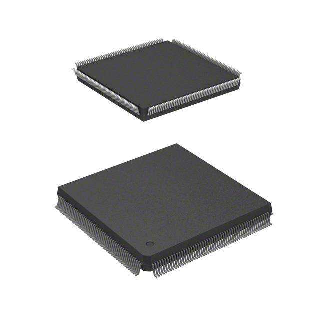
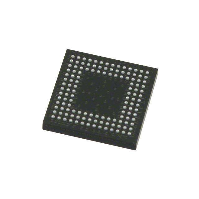
| 描述 | IC FPGA 108 I/O 144TQFP |
| 产品分类 | |
| I/O数 | 108 |
| LAB/CLB数 | 176 |
| 品牌 | Xilinx Inc |
| 数据手册 | |
| 产品图片 |
|
| 产品型号 | XC3S50AN-4TQG144C |
| PCN其它 | |
| PCN设计/规格 | |
| rohs | 无铅 / 符合限制有害物质指令(RoHS)规范要求 |
| 产品系列 | Spartan®-3AN |
| 产品培训模块 | http://www.digikey.cn/PTM/IndividualPTM.page?site=cn&lang=zhs&ptm=16177 |
| 产品目录页面 | |
| 供应商器件封装 | 144-TQFP(20x20) |
| 其它名称 | 122-1555 |
| 安装类型 | 表面贴装 |
| 封装/外壳 | 144-LQFP |
| 工作温度 | 0°C ~ 85°C |
| 总RAM位数 | 55296 |
| 栅极数 | 50000 |
| 标准包装 | 60 |
| 电压-电源 | 1.14 V ~ 1.26 V |
| 逻辑元件/单元数 | 1584 |


- 商务部:美国ITC正式对集成电路等产品启动337调查
- 曝三星4nm工艺存在良率问题 高通将骁龙8 Gen1或转产台积电
- 太阳诱电将投资9.5亿元在常州建新厂生产MLCC 预计2023年完工
- 英特尔发布欧洲新工厂建设计划 深化IDM 2.0 战略
- 台积电先进制程称霸业界 有大客户加持明年业绩稳了
- 达到5530亿美元!SIA预计今年全球半导体销售额将创下新高
- 英特尔拟将自动驾驶子公司Mobileye上市 估值或超500亿美元
- 三星加码芯片和SET,合并消费电子和移动部门,撤换高东真等 CEO
- 三星电子宣布重大人事变动 还合并消费电子和移动部门
- 海关总署:前11个月进口集成电路产品价值2.52万亿元 增长14.8%

PDF Datasheet 数据手册内容提取
1 Spartan-3AN FPGA Family Data Sheet DS557 January 9, 2019 Product Specification Module 1: Module 3: Introduction and Ordering Information DC and Switching Characteristics DS557(v4.3) January 9, 2019 DS557 (v4.3) January 9, 2019 (cid:129) Introduction (cid:129) DC Electrical Characteristics (cid:129) Features (cid:129) Absolute Maximum Ratings (cid:129) Architectural Overview (cid:129) Supply Voltage Specifications (cid:129) Configuration Overview (cid:129) Recommended Operating Conditions (cid:129) In-system Flash Memory Overview (cid:129) Switching Characteristics (cid:129) General I/O Capabilities (cid:129) I/O Timing (cid:129) Supported Packages and Package Marking (cid:129) Configurable Logic Block (CLB) Timing (cid:129) Ordering Information (cid:129) Multiplier Timing (cid:129) Block RAM Timing Module 2: (cid:129) Digital Clock Manager (DCM) Timing Functional Description (cid:129) Suspend Mode Timing DS557 (v4.3) January 9, 2019 (cid:129) Device DNA Timing (cid:129) Configuration and JTAG Timing The functionality of the Spartan®-3AN FPGA family is described in the following documents: Module 4: Pinout Descriptions (cid:129) UG331: Spartan-3 Generation FPGA User Guide (cid:129) Clocking Resources DS557 (v4.3) January 9, 2019 (cid:129) Digital Clock Managers (DCMs) (cid:129) Pin Descriptions (cid:129) Block RAM (cid:129) Package Overview (cid:129) Configurable Logic Blocks (CLBs) (cid:129) Pinout Tables - Distributed RAM (cid:129) Footprint Diagrams - SRL16 Shift Registers - Carry and Arithmetic Logic Table 1: Production Status of Spartan-3AN FPGAs (cid:129) I/O Resources Spartan-3AN FPGA Status (cid:129) Embedded Multiplier Blocks (cid:129) Programmable Interconnect XC3S50AN Production (cid:129) ISE® Design Tools and IP Cores XC3S200AN Production (cid:129) Embedded Processing and Control Solutions (cid:129) Pin Types and Package Overview XC3S400AN Production (cid:129) Package Drawings XC3S700AN Production (cid:129) Powering FPGAs XC3S1400AN Production (cid:129) Power Management (cid:129) UG332: Spartan-3 Generation Configuration User Guide Additional information on the Spartan-3AN family can be (cid:129) Configuration Overview found at: (cid:129) Configuration Pins and Behavior (cid:129) Bitstream Sizes http://www.xilinx.com/support/index.html/content/xilinx/en/s (cid:129) Detailed Descriptions by Mode upportNav/silicon_devices/fpga/spartan-3an.html. - Self-contained In-System Flash mode - Master Serial Mode using Platform Flash PROM - Master SPI Mode using Commodity Serial Flash - Master BPI Mode using Commodity Parallel Flash - Slave Parallel (SelectMAP) using a Processor - Slave Serial using a Processor - JTAG Mode (cid:129) ISE iMPACT Programming Examples (cid:129) MultiBoot Reconfiguration (cid:129) Design Authentication using Device DNA (cid:129) UG333: Spartan-3AN In-System Flash User Guide (cid:129) UG334: Spartan-3AN Starter Kit User Guide © Copyright 2007–2019 Xilinx, Inc. Xilinx, the Xilinx logo, Artix, ISE, Kintex, Spartan, Virtex, Vivado, Zynq, and other designated brands included herein are trademarks of Xilinx in the United States and other countries. PCI and PCI-X are trademarks of PCI-SIG and used under license. All other trademarks are the property of their respective owners. DS557 January 9, 2019 www.xilinx.com Send Feedback Product Specification 1
9 Spartan-3AN FPGA Family: Introduction and Ordering Information DS557(v4.3) January 9, 2019 Product Specification Introduction The Spartan®-3AN FPGA family combines the best attributes of a (cid:129) Buried configuration interface leading edge, low cost FPGA with nonvolatile technology across a (cid:129) Unique Device DNA serial number in each device for broad range of densities. The family combines all the features of design Authentication to prevent unauthorized copying the Spartan-3A FPGA family plus leading technology in-system (cid:129) Flash memory sector protection and lockdown Flash memory for configuration and nonvolatile data storage. (cid:129) Configuration watchdog timer automatically recovers from The Spartan-3AN FPGAs are part of the Extended Spartan-3A configuration errors family, which also includes the Spartan-3A FPGAs and the higher (cid:129) Suspend mode reduces system power consumption density Spartan-3A DSP FPGAs. The Spartan-3AN FPGA family (cid:129) Retains all design state and FPGA configuration data is excellent for space-constrained applications such as blade (cid:129) Fast response time, typically less than 100 μs servers, medical devices, automotive infotainment, telematics, GPS, and other small consumer products. Combining FPGA and (cid:129) Full hot-swap compliance Flash technology minimizes chip count, PCB traces and overall (cid:129) Multi-voltage, multi-standard SelectIO™ interface pins size while increasing system reliability. (cid:129) Up to 502 I/O pins or 227 differential signal pairs The Spartan-3AN FPGA internal configuration interface is (cid:129) LVCMOS, LVTTL, HSTL, and SSTL single-ended signal completely self-contained, increasing design security. The family standards maintains full support for external configuration. The Spartan-3AN (cid:129) 3.3V, 2.5V, 1.8V, 1.5V, and 1.2V signaling FPGA is the world’s first nonvolatile FPGA with MultiBoot, (cid:129) Up to 24 mA output drive supporting two or more configuration files in one device, allowing (cid:129) 3.3V ±10% compatibility and hot swap compliance alternative configurations for field upgrades, test modes, or (cid:129) 622+ Mb/s data transfer rate per I/O multiple system configurations. (cid:129) DDR/DDR2 SDRAM support up to 400 Mb/s Features (cid:129) LVDS, RSDS, mini-LVDS, PPDS, and HSTL/SSTL (cid:129) The new standard for low cost nonvolatile FPGA solutions differential I/O (cid:129) Abundant, flexible logic resources (cid:129) Eliminates traditional nonvolatile FPGA limitations with the advanced 90 nm Spartan-3A device feature set (cid:129) Densities up to 25,344 logic cells (cid:129) Memory, multipliers, DCMs, SelectIO, hot swap, power (cid:129) Optional shift register or distributed RAM support management, etc. (cid:129) Enhanced 18 x 18 multipliers with optional pipeline (cid:129) Integrated robust configuration memory (cid:129) Hierarchical SelectRAM™ memory architecture (cid:129) Saves board space (cid:129) Up to 576 Kbits of dedicated block RAM (cid:129) Improves ease-of-use (cid:129) Up to 176 Kbits of efficient distributed RAM (cid:129) Simplifies design (cid:129) Up to eight Digital Clock Managers (DCMs) (cid:129) Reduces support issues (cid:129) Eight global clocks and eight additional clocks per each half (cid:129) Plentiful amounts of nonvolatile memory available to the user of device, plus abundant low-skew routing (cid:129) Up to 11+Mb available (cid:129) Complete Xilinx® ISE® and WebPACK™ software (cid:129) MultiBoot support development system support (cid:129) Embedded processing and code shadowing (cid:129) MicroBlaze™ and PicoBlaze embedded processor cores (cid:129) Scratchpad memory (cid:129) Fully compliant 32-/64-bit 33 MHz PCI™ technology support (cid:129) Robust 100K Flash memory program/erase cycles (cid:129) Low-cost QFP and BGA Pb-free (RoHS) packaging options (cid:129) 20 years Flash memory data retention (cid:129) Pin-compatible with the same packages in the Spartan-3A FPGA family (cid:129) Security features provide bitstream anti-cloning protection Table 2: Summary of Spartan-3AN FPGA Attributes System Equivalent Distributed Block RAM Dedicated Maximum Max Differential Bitstream In-System Device Gates Logic Cells CLBs Slices RAM Bits(1) Bits(1) Multipliers DCMs User I/O I/O Pairs Size(1) Flash Bits XC3S50AN 50K 1,584 176 704 11K 54K 3 2 108 50 427K 1M(2) XC3S200AN 200K 4,032 448 1,792 28K 288K 16 4 195 90 1,168K 4M XC3S400AN 400K 8,064 896 3,584 56K 360K 20 4 311 142 1,842K 4M XC3S700AN 700K 13,248 1,472 5,888 92K 360K 20 8 372 165 2,669K 8M XC3S1400AN 1400K 25,344 2,816 11,264 176K 576K 32 8 502 227 4,644K 16M Notes: 1. By convention, one Kb is equivalent to 1,024 bits and one Mb is equivalent to 1,024 Kb. 2. Maximum supported by Xilinx tools. See the customer notice XCN14003: Flash Wafer Fabrication Change and Gold (Au) To Copper (Cu) Transition for Spartan-3AN FPGA Devices. © Copyright 2007–2019 Xilinx, Inc. Xilinx, the Xilinx logo, Artix, ISE, Kintex, Spartan, Virtex, Vivado, Zynq, and other designated brands included herein are trademarks of Xilinx in the United States and other countries. PCI and PCI-X are trademarks of PCI-SIG and used under license. All other trademarks are the property of their respective owners. DS557(v4.3) January 9, 2019 www.xilinx.com Send Feedback Product Specification 2
Spartan-3AN FPGA Family: Introduction and Ordering Information Architectural Overview The Spartan-3AN FPGA architecture is compatible with that (cid:129) Digital Clock Manager (DCM) Blocks provide of the Spartan-3A FPGA. The architecture consists of five self-calibrating, fully digital solutions for distributing, fundamental programmable functional elements: delaying, multiplying, dividing, and phase-shifting clock signals. (cid:129) Configurable Logic Blocks (CLBs) contain flexible Look-Up Tables (LUTs) that implement logic plus These elements are organized as shown in Figure1. A dual storage elements used as flip-flops or latches. ring of staggered IOBs surrounds a regular array of CLBs. Each device has two columns of block RAM except for the (cid:129) Input/Output Blocks (IOBs) control the flow of data XC3S50AN, which has one column. Each RAM column between the I/O pins and the internal logic of the consists of several 18-Kbit RAM blocks. Each block RAM is device. IOBs support bidirectional data flow plus associated with a dedicated multiplier. The DCMs are 3-state operation. They support a variety of signal positioned in the center with two at the top and two at the standards, including several high-performance bottom of the device. The XC3S50AN has DCMs only at the differential standards. Double Data-Rate (DDR) top, while the XC3S700AN and XC3S1400AN add two registers are included. DCMs in the middle of the two columns of block RAM and (cid:129) Block RAM provides data storage in the form of multipliers. 18-Kbit dual-port blocks. The Spartan-3AN FPGA features a rich network of traces (cid:129) Multiplier Blocks accept two 18-bit binary numbers as that interconnect all five functional elements, transmitting inputs and calculate the product. signals among them. Each functional element has an associated switch matrix that permits multiple connections to the routing. X-Ref Target - Figure 1 IOBs CLB M A er DCM Block R Multipli IOOBBss DDCCMM er pli CLBs ulti OBs DCM M / M OBs I RA I k c o Bl IOBs DS557-1_01_122006 Notes: 1. The XC3S700AN and XC3S1400AN have two additional DCMs on both the left and right sides as indicated by the dashed lines. The XC3S50AN has only two DCMs at the top and only one Block RAM/Multiplier column. Figure 1: Spartan-3AN Family Architecture DS557(v4.3) January 9, 2019 www.xilinx.com Send Feedback Product Specification 3
Spartan-3AN FPGA Family: Introduction and Ordering Information X-Ref Target - Figure 2 Spartan-3AN FPGA ‘0’ M2 VCCAUX 3.3V Configure from internal ‘1’ M1 INIT_B flash memory Indicates when ‘1’ M0 DONE configuration is finished DS557-1_06_082810 Figure 2: Spartan-3AN FPGA Configuration Interface from Internal SPI Flash Memory Configuration In-System Flash Memory Spartan-3AN FPGAs are programmed by loading Each Spartan-3AN FPGA contains abundant integrated SPI configuration data into robust, reprogrammable, static serial Flash memory, shown in Table3, used primarily to CMOS configuration latches (CCLs) that collectively control store the FPGA’s configuration bitstream. However, the all functional elements and routing resources. The FPGA’s Flash memory array is large enough to store at least two configuration data is stored on-chip in nonvolatile Flash MultiBoot FPGA configuration bitstreams or nonvolatile memory, or externally in a PROM or some other nonvolatile data required by the FPGA application, such as medium, either on or off the board. After applying power, the code-shadowed MicroBlaze processor applications. configuration data is written to the FPGA using any of seven Table 3: Spartan-3AN Device In-System Flash Memory different modes: Additional (cid:129) Configure from internal SPI Flash memory (Figure2) Total Flash FPGA Flash Part Number Memory Bitstream (cid:129) Completely self-contained Memory (Bits) (Bits) (Bits)(1) (cid:129) Reduced board space (cid:129) Easy-to-use configuration interface XC3S50AN 1,081,344(2) 437,312 642,048 (cid:129) Master Serial from a Xilinx Platform Flash PROM XC3S200AN 4,325,376 1,196,128 3,127,872 (cid:129) Serial Peripheral Interface (SPI) from an external XC3S400AN 4,325,376 1,886,560 2,437,248 industry-standard SPI serial Flash XC3S700AN 8,650,752 2,732,640 5,917,824 (cid:129) Byte Peripheral Interface (BPI) Up from an XC3S1400AN 17,301,504 4,755,296 12,545,280 industry-standard x8 or x8/x16 parallel NOR Flash Notes: (cid:129) Slave Serial, typically downloaded from a processor 1. Aligned to next available page location. (cid:129) Slave Parallel, typically downloaded from a processor 2. Maximum supported by Xilinx tools. (cid:129) Boundary-Scan (JTAG), typically downloaded from a After configuration, the FPGA design has full access to the processor or system tester in-system Flash memory via an internal SPI interface; the The MultiBoot feature stores multiple configuration files in control logic is implemented with FPGA logic. Additionally, the on-chip Flash, providing extended life with field the FPGA application itself can store nonvolatile data or upgrades. MultiBoot also supports multiple system provide live, in-system Flash updates. solutions with a single board to minimize inventory and The Spartan-3AN device in-system Flash memory supports simplify the addition of new features, even in the field. leading-edge serial Flash features. Flexibility is maintained to do additional MultiBoot configurations via the external configuration method. (cid:129) Small page size (264 or 528 bytes) simplifies nonvolatile data storage The Spartan-3AN device authentication protocol prevents (cid:129) Randomly accessible, byte addressable cloning. Design cloning, unauthorized overbuilding, and complete reverse engineering have driven device security (cid:129) Up to 66 MHz serial data transfers requirements to higher and higher levels. Authentication (cid:129) SRAM page buffers moves the security from bitstream protection to the next (cid:129) Read Flash data while programming another Flash generation of design-level security protecting both the page design and embedded microcode. The authentication (cid:129) EEPROM-like byte write functionality algorithm is entirely user defined, implemented using FPGA (cid:129) Two buffers in most devices, one in XC3S50AN logic. Every product, generation, or design can have a different algorithm and functionality to enhance security. (cid:129) Page, Block, and Sector Erase DS557(v4.3) January 9, 2019 www.xilinx.com Send Feedback Product Specification 4
Spartan-3AN FPGA Family: Introduction and Ordering Information (cid:129) Sector-based data protection and security features I/O Capabilities (cid:129) Sector Protect: Write- and erase-protect a sector The Spartan-3AN FPGA SelectIO interface supports many (changeable) popular single-ended and differential standards. Table4 (cid:129) Sector Lockdown: Sector data is unchangeable shows the number of user I/Os as well as the number of (permanent) differential I/O pairs available for each device/package (cid:129) 128-byte Security Register combination. Some of the user I/Os are unidirectional, (cid:129) Separate from FPGA’s unique Device DNA input-only pins as indicated in Table4. identifier Spartan-3AN FPGAs support the following single-ended (cid:129) 64-byte factory-programmed identifier unique to standards: the in-system Flash memory (cid:129) 3.3V low-voltage TTL (LVTTL) (cid:129) 64-byte one-time programmable, user-programmable field (cid:129) Low-voltage CMOS (LVCMOS) at 3.3V, 2.5V, 1.8V, 1.5V, or 1.2V (cid:129) 100,000 Program/Erase cycles (cid:129) 3.3V PCI at 33 MHz or 66 MHz (cid:129) 20-year data retention (cid:129) HSTL I, II, and III at 1.5V and 1.8V, commonly used in (cid:129) Comprehensive programming support memory applications (cid:129) In-system prototype programming via JTAG using (cid:129) SSTL I and II at 1.8V, 2.5V, and 3.3V, commonly used Xilinx Platform Cable USB and iMPACT software for memory applications (cid:129) Product programming support using BPM Microsystems programmers with appropriate Spartan-3AN FPGAs support the following differential programming adapter standards: (cid:129) Design examples demonstrating in-system (cid:129) LVDS, mini-LVDS, RSDS, and PPDS I/O at 2.5V or programming from a Spartan-3AN FPGA 3.3V application (cid:129) Bus LVDS I/O at 2.5V (cid:129) TMDS I/O at 3.3V (cid:129) Differential HSTL and SSTL I/O (cid:129) LVPECL inputs at 2.5V or 3.3V Table 4: Available User I/Os and Differential (Diff) I/O Pairs TQ144 FT256 FG400 FG484 FG676 Package(1) TQG144 FTG256 FGG400 FGG484 FGG676 Body Size (mm) 20x20(2) 17x17 21x21 23x23 27x27 Device(3) User Diff User Diff User Diff User Diff User Diff 108(4) 50 144(5) 64(5) XC3S50AN – – – – – – (7) (24) (32) (32) 195 90 XC3S200AN – – – – – – – – (35) (50) 195 90 311 142 XC3S400AN – – – – – – (35) (50) (63) (78) 372 165 XC3S700AN – – – – – – – – (84) (93) 375(5) 165(5) 502 227 XC3S1400AN – – – – – – (87) (93) (94) (131) Notes: 1. See Pb and Pb-Free Packaging, page7 for details on Pb and Pb-free packaging options. 2. The footprint for the TQ(G)144 (22mm x 22mm) package is larger than the package body. 3. Each Spartan-3AN FPGA has a pin-compatible Spartan-3A FPGA equivalent, although Spartan-3A FPGAs do not have internal SPI flash and offer more part/package combinations. 4. The number shown in bold indicates the maximum number of I/O and input-only pins. The number shown in (italics) indicates the number of input-only pins. The differential (Diff) input-only pin count includes both differential pairs on input-only pins and differential pairs on I/O pins within I/O banks that are restricted to differential inputs. 5. Xilinx has issued a discontinuation notice for these highlighted devices/packages. For more information see XCN13016: Product Discontinuation Notice For Selected Spartan-3AN FPGA Products. DS557(v4.3) January 9, 2019 www.xilinx.com Send Feedback Product Specification 5
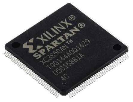
Spartan-3AN FPGA Family: Introduction and Ordering Information Package Marking Figure3 provides a top marking example for Spartan-3AN The “5C” and “4I” Speed Grade/Temperature Range part FPGAs in the quad-flat packages. Figure4 shows the top combinations may be dual marked as “5C/4I”. Devices marking for Spartan-3AN FPGAs in BGA packages. The with the dual mark can be used as either -5C or -4I devices. markings for the BGA packages are nearly identical to those Devices with a single mark are only guaranteed for the for the quad-flat packages, except that the marking is marked speed grade and temperature range. rotated with respect to the ball A1 indicator. X-Ref Target - Figure 3 Mask Revision Code Fabrication Code R SPARTANR Process Technology Device Type XC3S50ANTM Package TQG144AGQ0725 Date Code D1234567A Speed Grade 4C Lot Code Temperature Range Pin P1 DS557-1_02_080107 Figure 3: Spartan-3AN FPGA QFP Package Marking Example X-Ref Target - Figure 4 Mask Revision Code BGA Ball A1 R Fabrication Code SPARTANR Process Code Device Type XC3S200ANTM Package FTG256AGQ0725 Date Code D1234567A 4C Lot Code Speed Grade Temperature Range DS557-1_03_080107 Figure 4: Spartan-3AN FPGA BGA Package Marking Example DS557(v4.3) January 9, 2019 www.xilinx.com Send Feedback Product Specification 6
Spartan-3AN FPGA Family: Introduction and Ordering Information Pb and Pb-Free Packaging Spartan-3AN FPGAs are available in both leaded (Pb) and Pb-free packaging options (see Table5). The Pb-free packages are available for all devices and include a ‘G’ character in the ordering code. Leaded (non-Pb-free) packages are available for selected devices. The ordering code for the leaded devices does not have an extra ‘G’. Leaded and Pb-free devices have the same pin-out. Table 5: Pb and Pb-Free Package Options Pins 144 256 400 484 676 Type TQFP FTBGA FBGA FBGA FBGA Material Pb-Free Pb Pb-Free Pb Pb-Free Pb Pb-Free Pb Pb-Free Pb Device Speed Range TQG144 TQ144 FTG256 FT256 FGG400 FG400 FGG484 FG484 FGG676 FG676 XC3S50AN -4 C, I ✔ SCD4100(1) Note3 Note3 -5 C ✔ Note2 Note3 Note3 XC3S200AN -4 C, I ✔ ✔ -5 C ✔ ✔ XC3S400AN -4 C, I ✔ ✔ ✔ ✔ -5 C ✔ ✔ ✔ Note2 XC3S700AN -4 C, I ✔ ✔ -5 C ✔ Note2 XC3S1400AN -4 C, I Note3 Note3 ✔ ✔ -5 C Note3 Note3 ✔ Note2 Notes: 1. To order a Pb package for the XC3S50AN -4 option, append SCD4100 to the part number (XC3S50AN-4TQ144C4100). 2. For Pb packaging for these options, contact your Xilinx sales representative. 3. Xilinx has issued a discontinuation notice for these highlighted devices/packages. For more information see XCN13016: Product Discontinuation Notice For Selected Spartan-3AN FPGA Products. DS557(v4.3) January 9, 2019 www.xilinx.com Send Feedback Product Specification 7
Spartan-3AN FPGA Family: Introduction and Ordering Information Ordering Information X-Ref Target - Figure 5 Example: XC3S50AN -4 TQG144 C Device Type Temperature Range: C = Commercial (T = 0oC to 85oC) J Speed Grade I = Industrial (T = -40oC to 100oC) J Package Type/Number of Pins DS557-1_05_101109 Figure 5: Device Numbering Format Device Speed Grade Package Type / Number of Pins Temperature Range (T ) J XC3S50AN -4 Standard PerformanceTQ144/ 144-pin Thin Quad Flat Pack (TQFP) C Commercial (0°C to 85°C) TQG144 XC3S200AN -5 High Performance(1) FT256/ 256-ball Fine-Pitch Thin Ball Grid Array (FTBGA) I Industrial (–40°C to 100°C) FTG256 XC3S400AN FG400/ 400-ball Fine-Pitch Ball Grid Array (FBGA) FGG400 XC3S700AN FG484/ 484-ball Fine-Pitch Ball Grid Array (FBGA) FGG484 XC3S1400AN FG676/ 676-ball Fine-Pitch Ball Grid Array (FBGA) FGG676 Notes: 1. The -5 speed grade is exclusively available in the Commercial temperature range. 2. See Table4 and Table5 for available package combinations. DS557(v4.3) January 9, 2019 www.xilinx.com Send Feedback Product Specification 8
Spartan-3AN FPGA Family: Introduction and Ordering Information Revision History The following table shows the revision history for this document. Date Version Revision 02/26/2007 1.0 Initial release. 08/16/2007 2.0 Updated for Production release of initial device. 09/12/2007 2.0.1 Noted that only dual-mark devices are guaranteed for both -4I and -5C. 12/12/2007 3.0 Updated to Production status with Production release of final family member, XC3S50AN. Noted that non-Pb-free packages may be available for selected devices. 06/02/2008 3.1 Minor updates. 11/19/2009 3.2 Updated document throughout to reflect availability of Pb package options. Added references to the Extended Spartan-3A family. Removed table note 2 from Table2. In Table4, added Pb packages, added table note 4, and updated table note 2. Added Table5. 12/02/2010 4.0 Updated Notice of Disclaimer. 04/01/2011 4.1 In Table2, revised the Maximum Differential I/O Pairs and Maximum User I/O values for the XC3S50AN. In Table4, added packages to the XC3S50AN, XC3S400AN, and XC3S1400AN. Updated Pb and Pb-Free Packaging section and Table5 to include the new device/package combinations for the XC3S50AN, XC3S400AN, and XC3S1400AN. 06/11/2014 4.2 In Table2, revised the XC3S50AN values in Maximum User I/O and Max Differential I/O Pairs columns, and added Note2 to the In-System Flash Bits column. In Table3, added the same Note2. Descriptions of these changes and further links to the product changes are outlined in the customer notice XCN14003: Flash Wafer Fabrication Change and Gold (Au) To Copper (Cu) Transition for Spartan-3AN FPGA Devices. Xilinx has issued a discontinuation notice for the XC3S50AN in the FT(G)256 package and the XC3S1400AN in the FG(G)484 package. See XCN13016: Product Discontinuation Notice For Selected Spartan-3AN FPGA Products. This customer notice is highlighted in Table4 and Table5. Updated Notice of Disclaimer. 01/09/2019 4.3 Updated for Lead-Frame Plating Composition Change For Legacy Eutectic Products (XCN18024). Notice of Disclaimer The information disclosed to you hereunder (the “Materials”) is provided solely for the selection and use of Xilinx products. To the maximum extent permitted by applicable law: (1) Materials are made available "AS IS" and with all faults, Xilinx hereby DISCLAIMS ALL WARRANTIES AND CONDITIONS, EXPRESS, IMPLIED, OR STATUTORY, INCLUDING BUT NOT LIMITED TO WARRANTIES OF MERCHANTABILITY, NON-INFRINGEMENT, OR FITNESS FOR ANY PARTICULAR PURPOSE; and (2) Xilinx shall not be liable (whether in contract or tort, including negligence, or under any other theory of liability) for any loss or damage of any kind or nature related to, arising under, or in connection with, the Materials (including your use of the Materials), including for any direct, indirect, special, incidental, or consequential loss or damage (including loss of data, profits, goodwill, or any type of loss or damage suffered as a result of any action brought by a third party) even if such damage or loss was reasonably foreseeable or Xilinx had been advised of the possibility of the same. Xilinx assumes no obligation to correct any errors contained in the Materials or to notify you of updates to the Materials or to product specifications. You may not reproduce, modify, distribute, or publicly display the Materials without prior written consent. Certain products are subject to the terms and conditions of Xilinx’s limited warranty, please refer to Xilinx’s Terms of Sale which can be viewed at www.xilinx.com/legal.htm#tos; IP cores may be subject to warranty and support terms contained in a license issued to you by Xilinx. Xilinx products are not designed or intended to be fail-safe or for use in any application requiring fail-safe performance; you assume sole risk and liability for use of Xilinx products in such critical applications, please refer to Xilinx’s Terms of Sale which can be viewed at www.xilinx.com/legal.htm#tos. AUTOMOTIVE APPLICATIONS DISCLAIMER AUTOMOTIVE PRODUCTS (IDENTIFIED AS “XA” IN THE PART NUMBER) ARE NOT WARRANTED FOR USE IN THE DEPLOYMENT OF AIRBAGS OR FOR USE IN APPLICATIONS THAT AFFECT CONTROL OF A VEHICLE (“SAFETY APPLICATION”) UNLESS THERE IS A SAFETY CONCEPT OR REDUNDANCY FEATURE CONSISTENT WITH THE ISO 26262 AUTOMOTIVE SAFETY STANDARD (“SAFETY DESIGN”). CUSTOMER SHALL, PRIOR TO USING OR DISTRIBUTING ANY SYSTEMS THAT INCORPORATE PRODUCTS, THOROUGHLY TEST SUCH SYSTEMS FOR SAFETY PURPOSES. USE OF PRODUCTS IN A SAFETY APPLICATION WITHOUT A SAFETY DESIGN IS FULLY AT THE RISK OF CUSTOMER, SUBJECT ONLY TO APPLICABLE LAWS AND REGULATIONS GOVERNING LIMITATIONS ON PRODUCT LIABILITY. DS557(v4.3) January 9, 2019 www.xilinx.com Send Feedback Product Specification 9
11 Spartan-3AN FPGA Family: Functional Description DS557 (v4.3) January 9, 2019 Product Specification Spartan-3AN FPGA Design Documentation The functionality of the Spartan®-3AN FPGA family is (cid:129) UG333: Spartan-3AN FPGA In-System Flash User described in the following documents. The topics covered in Guide each guide are listed below: (cid:129) For FPGA applications that write to or read from • DS706: Extended Spartan-3A Family Overview the In-System Flash memory after configuration (cid:129) UG331: Spartan-3 Generation FPGA User Guide (cid:129) SPI_ACCESS interface (cid:129) Clocking Resources (cid:129) In-System Flash memory architecture (cid:129) Digital Clock Managers (DCMs) (cid:129) Read, program, and erase commands (cid:129) Block RAM (cid:129) Status registers (cid:129) Configurable Logic Blocks (CLBs) (cid:129) Sector Protection and Sector Lockdown features - Distributed RAM (cid:129) Security Register with Unique Identifier - SRL16 Shift Registers - Carry and Arithmetic Logic Create a Xilinx user account and sign up to receive (cid:129) I/O Resources automatic e-mail notification whenever this data sheet or (cid:129) Embedded Multiplier Blocks the associated user guides are updated. (cid:129) Programmable Interconnect (cid:129) Sign Up for Alerts on Xilinx.com (cid:129) ISE® Design Tools https://secure.xilinx.com/webreg/register.do?group=my (cid:129) IP Cores profile&languageID=1 (cid:129) Embedded Processing and Control Solutions (cid:129) Pin Types and Package Overview Spartan-3AN FPGA Starter Kit (cid:129) Package Drawings For specific hardware examples, please see the (cid:129) Powering FPGAs Spartan-3AN FPGA Starter Kit board web page, which has (cid:129) Power Management links to various design examples and the user guide. (cid:129) UG332: Spartan-3 Generation Configuration (cid:129) Spartan-3AN FPGA Starter Kit Board Page User Guide http://www.xilinx.com/s3anstarter (cid:129) Configuration Overview (cid:129) UG334: Spartan-3AN FPGA Starter Kit User Guide - Configuration Pins and Behavior - Bitstream Sizes Related Product Families (cid:129) Detailed Descriptions by Mode - Master Serial Mode using Xilinx® Platform The Spartan-3AN FPGA family is generally compatible with Flash the Spartan-3A FPGA family. - Master SPI Mode using SPI Serial Flash (cid:129) DS529: Spartan-3A FPGA Family Data Sheet PROM - Internal Master SPI Mode - Master BPI Mode using Parallel NOR Flash - Slave Parallel (SelectMAP) using a Processor - Slave Serial using a Processor - JTAG Mode (cid:129) ISE iMPACT Programming Examples (cid:129) MultiBoot Reconfiguration (cid:129) Design Authentication using Device DNA © Copyright 2007–2019 Xilinx, Inc. Xilinx, the Xilinx logo, Artix, ISE, Kintex, Spartan, Virtex, Vivado, Zynq, and other designated brands included herein are trademarks of Xilinx in the United States and other countries. PCI and PCI-X are trademarks of PCI-SIG and used under license. All other trademarks are the property of their respective owners. DS557 (v4.3) January 9, 2019 www.xilinx.com Send Feedback Product Specification 10
Spartan-3AN FPGA Family: Functional Description Revision History The following table shows the revision history for this document. Date Version Revision 02/26/2007 1.0 Initial release. 08/16/2007 2.0 Updated for Production release of initial device. 09/12/2007 2.0.1 Minor updates to text. 09/24/2007 2.1 Added note that In-System Flash commands were not supported by simulation until ISE 10.1 software. 12/12/2007 3.0 Updated to Production status with Production release of final family member, XC3S50AN. Noted that SPI_ACCESS simulation is supported in ISE 10.1 software. Updated links. 06/02/2008 3.1 Minor updates. 11/19/2009 3.2 In the Spartan-3AN FPGA Design Documentation section, added link to DS706, Extended Spartan-3A Family Overview and removed references to older software versions. 12/02/2010 4.0 Updated link to sign up for Alerts and updated Notice of Disclaimer. 04/01/2011 4.1 Added the FT(G)256 package selection for the XC3S50AN and XC3S400AN devices and the FG(G)484 package selection for the XC3S1400AN device throughout this data sheet. 06/11/2014 4.2 Xilinx has issued a discontinuation notice for the XC3S50AN in the FT(G)256 package and the XC3S1400AN in the FG(G)484 package. See XCN13016: Product Discontinuation Notice For Selected Spartan-3AN FPGA Products. Updated Notice of Disclaimer. 01/09/2019 4.3 Updated for Lead-Frame Plating Composition Change For Legacy Eutectic Products (XCN18024). Notice of Disclaimer The information disclosed to you hereunder (the “Materials”) is provided solely for the selection and use of Xilinx products. To the maximum extent permitted by applicable law: (1) Materials are made available "AS IS" and with all faults, Xilinx hereby DISCLAIMS ALL WARRANTIES AND CONDITIONS, EXPRESS, IMPLIED, OR STATUTORY, INCLUDING BUT NOT LIMITED TO WARRANTIES OF MERCHANTABILITY, NON-INFRINGEMENT, OR FITNESS FOR ANY PARTICULAR PURPOSE; and (2) Xilinx shall not be liable (whether in contract or tort, including negligence, or under any other theory of liability) for any loss or damage of any kind or nature related to, arising under, or in connection with, the Materials (including your use of the Materials), including for any direct, indirect, special, incidental, or consequential loss or damage (including loss of data, profits, goodwill, or any type of loss or damage suffered as a result of any action brought by a third party) even if such damage or loss was reasonably foreseeable or Xilinx had been advised of the possibility of the same. Xilinx assumes no obligation to correct any errors contained in the Materials or to notify you of updates to the Materials or to product specifications. You may not reproduce, modify, distribute, or publicly display the Materials without prior written consent. Certain products are subject to the terms and conditions of Xilinx’s limited warranty, please refer to Xilinx’s Terms of Sale which can be viewed at www.xilinx.com/legal.htm#tos; IP cores may be subject to warranty and support terms contained in a license issued to you by Xilinx. Xilinx products are not designed or intended to be fail-safe or for use in any application requiring fail-safe performance; you assume sole risk and liability for use of Xilinx products in such critical applications, please refer to Xilinx’s Terms of Sale which can be viewed at www.xilinx.com/legal.htm#tos. AUTOMOTIVE APPLICATIONS DISCLAIMER AUTOMOTIVE PRODUCTS (IDENTIFIED AS “XA” IN THE PART NUMBER) ARE NOT WARRANTED FOR USE IN THE DEPLOYMENT OF AIRBAGS OR FOR USE IN APPLICATIONS THAT AFFECT CONTROL OF A VEHICLE (“SAFETY APPLICATION”) UNLESS THERE IS A SAFETY CONCEPT OR REDUNDANCY FEATURE CONSISTENT WITH THE ISO 26262 AUTOMOTIVE SAFETY STANDARD (“SAFETY DESIGN”). CUSTOMER SHALL, PRIOR TO USING OR DISTRIBUTING ANY SYSTEMS THAT INCORPORATE PRODUCTS, THOROUGHLY TEST SUCH SYSTEMS FOR SAFETY PURPOSES. USE OF PRODUCTS IN A SAFETY APPLICATION WITHOUT A SAFETY DESIGN IS FULLY AT THE RISK OF CUSTOMER, SUBJECT ONLY TO APPLICABLE LAWS AND REGULATIONS GOVERNING LIMITATIONS ON PRODUCT LIABILITY. DS557 (v4.3) January 9, 2019 www.xilinx.com Send Feedback Product Specification 11
70 Spartan-3AN FPGA Family: DC and Switching Characteristics DS557 (v4.3) January 9, 2019 Product Specification DC Electrical Characteristics In this section, specifications can be designated as All parameter limits are representative of worst-case supply Advance, Preliminary, or Production. These terms are voltage and junction temperature conditions. Unless defined as follows: otherwise noted, the published parameter values apply to all Spartan®-3AN devices. AC and DC characteristics Advance: Initial estimates are based on simulation, early are specified using the same numbers for both characterization, and/or extrapolation from the commercial and industrial grades. characteristics of other families. Values are subject to change. Use as estimates, not for production. Absolute Maximum Ratings Preliminary: Based on characterization. Further changes are not expected. Stresses beyond those listed under Table6: Absolute Maximum Ratings might cause permanent damage to the Production: These specifications are approved once the device. These are stress ratings only; functional operation silicon has been characterized over numerous production of the device at these or any other conditions beyond those lots. Parameter values are considered stable with no future listed under the Recommended Operating Conditions is not changes expected. implied. Exposure to absolute maximum conditions for extended periods of time adversely affects device reliability. Table 6: Absolute Maximum Ratings Symbol Description Conditions Min Max Units V Internal supply voltage –0.5 1.32 V CCINT V Auxiliary supply voltage –0.5 3.75 V CCAUX V Output driver supply voltage –0.5 3.75 V CCO V Input reference voltage –0.5 V +0.5 V REF CCO Voltage applied to all User I/O pins and Driver in a high-impedance state –0.95 4.6 V V dual-purpose pins IN Voltage applied to all Dedicated pins –0.5 4.6 V I Input clamp current per I/O pin –0.5V < V < (V + 0.5V)(1) – ±100 mA IK IN CCO Electrostatic Discharge Voltage Human body model – ±2000 V V Charged device model – ±500 V ESD Machine model – ±200 V T Junction temperature – 125 °C J T Storage temperature –65 150 °C STG Notes: 1. Upper clamp applies only when using PCI IOSTANDARDs. 1. For soldering guidelines, see UG112: Device Package User Guide and XAPP427: Implementation and Solder Reflow Guidelines for Pb-Free Packages. © Copyright 2007–2019 Xilinx, Inc. Xilinx, the Xilinx logo, Artix, ISE, Kintex, Spartan, Virtex, Vivado, Zynq, and other designated brands included herein are trademarks of Xilinx in the United States and other countries. PCI and PCI-X are trademarks of PCI-SIG and used under license. All other trademarks are the property of their respective owners. DS557 (v4.3) January 9, 2019 www.xilinx.com Send Feedback Product Specification 12
Spartan-3AN FPGA Family: DC and Switching Characteristics Power Supply Specifications Table 7: Supply Voltage Thresholds for Power-On Reset Symbol Description Min Max Units V Threshold for the V supply 0.4 1.0 V CCINTT CCINT V Threshold for the V supply 1.0 2.0 V CCAUXT CCAUX V Threshold for the V Bank 2 supply 1.0 2.0 V CCO2T CCO Notes: 1. When configuring from the In-System Flash, V must be in the recommended operating range; on power-up make sure V CCAUX CCAUX reaches at least 3.0V before INIT_B goes High to indicate the start of configuration. V , V , and V supplies to the FPGA can CCINT CCAUX CCO be applied in any order if this requirement is met. However, an external configuration source might have specific requirements. Check the data sheet for the attached configuration source. Apply V last for lowest overall power consumption (see the chapter called “Powering CCINT Spartan-3 Generation FPGAs” in UG331 for more information). 2. To ensure successful power-on, V , V Bank 2, and V supplies must rise through their respective threshold-voltage ranges with CCINT CCO CCAUX no dips at any point. Table 8: Supply Voltage Ramp Rate Symbol Description Min Max Units V Ramp rate from GND to valid V supply level 0.2 100 ms CCINTR CCINT V Ramp rate from GND to valid V supply level 0.2 100 ms CCAUXR CCAUX V Ramp rate from GND to valid V Bank 2 supply level 0.2 100 ms CCO2R CCO Notes: 1. When configuring from the In-System Flash, V must be in the recommended operating range; on power-up make sure V CCAUX CCAUX reaches at least 3.0V before INIT_B goes High to indicate the start of configuration. V , V , and V supplies to the FPGA can CCINT CCAUX CCO be applied in any order if this requirement is met. However, an external configuration source might have specific requirements. Check the data sheet for the attached configuration source. Apply V last for lowest overall power consumption (see the chapter called “Powering CCINT Spartan-3 Generation FPGAs” in UG331 for more information). 2. To ensure successful power-on, V , V Bank 2, and V supplies must rise through their respective threshold-voltage ranges with CCINT CCO CCAUX no dips at any point. Table 9: Supply Voltage Levels Necessary for Preserving CMOS Configuration Latch (CCL) Contents and RAM Data Symbol Description Min Units V V level required to retain CMOS Configuration Latch (CCL) and RAM data 1.0 V DRINT CCINT V V level required to retain CMOS Configuration Latch (CCL) and RAM data 2.0 V DRAUX CCAUX DS557 (v4.3) January 9, 2019 www.xilinx.com Send Feedback Product Specification 13
Spartan-3AN FPGA Family: DC and Switching Characteristics General Recommended Operating Conditions Table 10: General Recommended Operating Conditions Symbol Description Min Nominal Max Units T Junction temperature Commercial 0 – 85 °C J Industrial –40 – 100 °C V Internal supply voltage 1.14 1.20 1.26 V CCINT V (1) Output driver supply voltage 1.10 – 3.60 V CCO V Auxiliary supply voltage V =3.3V 3.00 3.30 3.60 V CCAUX CCAUX V (2) Input voltage PCI IOSTANDARD –0.5 – V +0.5 V IN CCO All other IP or IO_# –0.5 – 4.10 V IOSTANDARDs IO_Lxxy_#(3) –0.5 – 4.10 V T Input signal transition time(4) – – 500 ns IN Notes: 1. This V range spans the lowest and highest operating voltages for all supported I/O standards. Table13 lists the recommended V CCO CCO range specific to each of the single-ended I/O standards, and Table15 lists that specific to the differential standards. 2. See XAPP459, Eliminating I/O Coupling Effects when Interfacing Large-Swing Single-Ended Signals to User I/O Pins on Spartan-3 Families. 3. For single-ended signals that are placed on a differential-capable I/O, V of –0.2V to –0.5V is supported but can cause increased leakage IN between the two pins. See Parasitic Leakage in UG331, Spartan-3 Generation FPGA User Guide. 4. Measured between 10% and 90% V . Follow Signal Integrity recommendations. CCO DS557 (v4.3) January 9, 2019 www.xilinx.com Send Feedback Product Specification 14
Spartan-3AN FPGA Family: DC and Switching Characteristics General DC Characteristics for I/O Pins Table 11: General DC Characteristics of User I/O, Dual-Purpose, and Dedicated Pins Symbol Description Test Conditions Min Typ Max Units I (2) Leakage current at User I/O, Driver is in a high-impedance state, –10 – +10 µA L Input-only, Dual-Purpose, and V =0V or V max, sample-tested IN CCO Dedicated pins, FPGA powered I Leakage current on pins during All pins except INIT_B, PROG_B, DONE, and JTAG –10 – +10 µA HS hot socketing, FPGA unpowered pins when PUDC_B=1. INIT_B, PROG_B, DONE, and JTAG pins or other Add I + I µA HS RPU pins when PUDC_B=0. I (3) Current through pull-up resistor V = GND V or V = –151 –315 –710 µA RPU IN CCO CCAUX at User I/O, Dual-Purpose, 3.0V to 3.6V Input-only, and Dedicated pins. V = 2.3V to 2.7V –82 –182 –437 µA Dedicated pins are powered by CCO VCCAUX.(4) VCCO = 1.7V to 1.9V –36 –88 –226 µA V = 1.4V to 1.6V –22 –56 –148 µA CCO V = 1.14V to 1.26V –11 –31 –83 µA CCO R (3) Equivalent pull-up resistor value V = GND V = 3.0V to 3.6V 5.1 11.4 23.9 kΩ PU IN CCO at User I/O, Dual-Purpose, V = 2.3V to 2.7V 6.2 14.8 33.1 kΩ Input-only, and Dedicated pins CCO (based on IRPU per Note 3) VCCO = 1.7V to 1.9V 8.4 21.6 52.6 kΩ V = 1.4V to 1.6V 10.8 28.4 74.0 kΩ CCO V = 1.14V to 1.26V 15.3 41.1 119.4 kΩ CCO I (3) Current through pull-down V = V V = 3.0V to 3.6V 167 346 659 µA RPD IN CCO CCAUX resistor at User I/O, Dual-Purpose, Input-only, and Dedicated pins R (3) Equivalent pull-down resistor V = 3.0V to 3.6V V = 3.0V to 3.6V 5.5 10.4 20.8 kΩ PD CCAUX IN value at User I/O, Dual-Purpose, V = 2.3V to 2.7V 4.1 7.8 15.7 kΩ Input-only, and Dedicated pins IN (based on IRPD per Note 3) VIN = 1.7V to 1.9V 3.0 5.7 11.1 kΩ V = 1.4V to 1.6V 2.7 5.1 9.6 kΩ IN V = 1.14V to 1.26V 2.4 4.5 8.1 kΩ IN I V current per pin All V levels –10 – +10 µA REF REF CCO C Input capacitance – – – 10 pF IN R Resistance of optional differential V = 3.3V ± 10% LVDS_33, 90 100 115 Ω DT CCO termination circuit within a MINI_LVDS_33, differential I/O pair. Not available RSDS_33 on Input-only pairs. V = 2.5V ± 10% LVDS_25, 90 110 – Ω CCO MINI_LVDS_25, RSDS_25 Notes: 1. The numbers in this table are based on the conditions set forth in Table10. 2. For single-ended signals that are placed on a differential-capable I/O, V of –0.2V to –0.5V is supported but can cause increased leakage IN between the two pins. See Parasitic Leakage in UG331, Spartan-3 Generation FPGA User Guide. 3. This parameter is based on characterization. The pull-up resistance R = V / I . The pull-down resistance R =V /I . PU CCO RPU PD IN RPD 4. V must be 3.3V on Spartan-3AN FPGAs. V for Spartan-3A FPGAs can be either 3.3V or 2.5V. CCAUX CCAUX DS557 (v4.3) January 9, 2019 www.xilinx.com Send Feedback Product Specification 15
Spartan-3AN FPGA Family: DC and Switching Characteristics Quiescent Current Requirements Table 12: Spartan-3AN FPGA Quiescent Supply Current Characteristics Commercial Industrial Symbol Description Device Typical(2) Units Maximum(2) Maximum(2) I Quiescent V supply current XC3S50AN 2 20 30 mA CCINTQ CCINT XC3S200AN 7 50 70 mA XC3S400AN 10 85 125 mA XC3S700AN 13 120 185 mA XC3S1400AN 24 220 310 mA I Quiescent V supply current XC3S50AN 0.2 2 3 mA CCOQ CCO XC3S200AN 0.2 2 3 mA XC3S400AN 0.3 3 4 mA XC3S700AN 0.3 3 4 mA XC3S1400AN 0.3 3 4 mA I Quiescent V supply current XC3S50AN 3.1 8.1 10.1 mA CCAUXQ CCAUX XC3S200AN 5.1 12.1 15.1 mA XC3S400AN 5.1 18.1 24.1 mA XC3S700AN 6.1 28.1 34.1 mA XC3S1400AN 10.1 50.1 58.1 mA Notes: 1. The numbers in this table are based on the conditions set forth in Table10. 2. Quiescent supply current is measured with all I/O drivers in a high-impedance state and with all pull-up/pull-down resistors at the I/O pads disabled. The internal SPI Flash is deselected (CSB = High); the internal SPI Flash current is consumed on the V supply rail. Typical CCAUX values are characterized using typical devices at room temperature (T of 25°C at V = 1.2V, V = 3.3V, and V = 3.3V). The J CCINT CCO CCAUX maximum limits are tested for each device at the respective maximum specified junction temperature and at maximum voltage limits with V = 1.26V, V = 3.6V, and V = 3.6V. The FPGA is programmed with a “blank” configuration data file (that is, a design with no CCINT CCO CCAUX functional elements instantiated). For conditions other than those described above (for example, a design including functional elements), measured quiescent current levels will be different than the values in the table. 3. There are two recommended ways to estimate the total power consumption (quiescent plus dynamic) for a specific design: (cid:129) The Spartan-3AN FPGA Xilinx Power Estimator provides quick, approximate, typical estimates, and does not require a netlist of the design. (cid:129) Xilinx Power Analyzer uses a netlist as input to provide maximum estimates as well as more accurate typical estimates. For more information on power for the In-System Flash memory, see the Power Management chapter of UG333. 4. The maximum numbers in this table indicate the minimum current each power rail requires in order for the FPGA to power-on successfully. 5. For information on the power-saving Suspend mode, see XAPP480: Using Suspend Mode in Spartan-3 Generation FPGAs. Suspend mode typically saves 40% total power consumption compared to quiescent current. DS557 (v4.3) January 9, 2019 www.xilinx.com Send Feedback Product Specification 16
Spartan-3AN FPGA Family: DC and Switching Characteristics Single-Ended I/O Standards Table 13: Recommended Operating Conditions for User I/Os Using Single-Ended Standards IOSTANDARD VCCO for Drivers(2) VREF VIL VIH(3) Attribute Min (V) Nom (V) Max (V) Min (V) Nom (V) Max (V) Max (V) Min (V) LVTTL 3.0 3.3 3.6 0.8 2.0 LVCMOS33(4) 3.0 3.3 3.6 0.8 2.0 LVCMOS25(4)(5) 2.3 2.5 2.7 0.7 1.7 LVCMOS18 1.65 1.8 1.95 V is not used for 0.4 0.8 REF LVCMOS15 1.4 1.5 1.6 these I/O standards 0.4 0.8 LVCMOS12 1.1 1.2 1.3 0.4 0.7 PCI33_3(6) 3.0 3.3 3.6 0.3• V 0.5• V CCO CCO PCI66_3(6) 3.0 3.3 3.6 0.3• V 0.5• V CCO CCO HSTL_I 1.4 1.5 1.6 0.68 0.75 0.9 V – 0.1 V + 0.1 REF REF HSTL_III 1.4 1.5 1.6 – 0.9 – V – 0.1 V + 0.1 REF REF HSTL_I_18 1.7 1.8 1.9 0.8 0.9 1.1 V – 0.1 V + 0.1 REF REF HSTL_II_18 1.7 1.8 1.9 – 0.9 – V – 0.1 V + 0.1 REF REF HSTL_III_18 1.7 1.8 1.9 – 1.1 – V – 0.1 V + 0.1 REF REF SSTL18_I 1.7 1.8 1.9 0.833 0.900 0.969 V – 0.125 V + 0.125 REF REF SSTL18_II 1.7 1.8 1.9 0.833 0.900 0.969 V – 0.125 V + 0.125 REF REF SSTL2_I 2.3 2.5 2.7 1.13 1.25 1.38 V – 0.150 V + 0.150 REF REF SSTL2_II 2.3 2.5 2.7 1.13 1.25 1.38 V – 0.150 V + 0.150 REF REF SSTL3_I 3.0 3.3 3.6 1.3 1.5 1.7 V – 0.2 V + 0.2 REF REF SSTL3_II 3.0 3.3 3.6 1.3 1.5 1.7 V – 0.2 V + 0.2 REF REF Notes: 1. Descriptions of the symbols used in this table are as follows: V – the supply voltage for output drivers CCO V – the reference voltage for setting the input switching threshold REF V – the input voltage that indicates a Low logic level IL V – the input voltage that indicates a High logic level IH 2. In general, the V rails supply only output drivers, not input circuits. The exceptions are for LVCMOS25 inputs and for PCI™ I/O standards. CCO 3. For device operation, the maximum signal voltage (V max) can be as high as V max. See Table6. IH IN 4. There is approximately 100 mV of hysteresis on inputs using LVCMOS33 and LVCMOS25 I/O standards. 5. All Dedicated pins (PROG_B, DONE, SUSPEND, TCK, TDI, TDO, and TMS) draw power from the V rail and use the LVCMOS33 CCAUX standard. The Dual-Purpose configuration pins use the LVCMOS standard before the User mode. When using these pins as part of a standard 2.5V configuration interface, apply 2.5V to the V lines of Banks 0, 1, and 2 at power-on as well as throughout configuration. CCO 6. For information on PCI IP solutions, see www.xilinx.com/pci. The PCI IOSTANDARD is not supported on input-only pins. The PCIX IOSTANDARD is available and has equivalent characteristics but no PCI-X IP is supported. DS557 (v4.3) January 9, 2019 www.xilinx.com Send Feedback Product Specification 17
Spartan-3AN FPGA Family: DC and Switching Characteristics Table 14: DC Characteristics of User I/Os Using Table 14: DC Characteristics of User I/Os Using Single-Ended Standards Single-Ended Standards (Cont’d) Test Logic Level Test Logic Level IOSTANDARD Conditions Characteristics IOSTANDARD Conditions Characteristics Attribute IOL IOH VOL VOH Attribute IOL IOH VOL VOH (mA) (mA) Max (V) Min (V) (mA) (mA) Max (V) Min (V) LVTTL(3) 2 2 –2 0.4 2.4 HSTL_I(5) 8 –8 0.4 VCCO - 0.4 4 4 –4 HSTL_III(5) 24 –8 0.4 VCCO - 0.4 6 6 –6 HSTL_I_18 8 –8 0.4 VCCO - 0.4 8 8 –8 HSTL_II_18(5) 16 –16 0.4 VCCO - 0.4 12 12 –12 HSTL_III_18 24 –8 0.4 VCCO - 0.4 16 16 –16 SSTL18_I 6.7 –6.7 VTT – 0.475 VTT + 0.475 24 24 –24 SSTL18_II(5) 13.4 –13.4 VTT – 0.603 VTT + 0.603 LVCMOS33(3) 2 2 –2 0.4 VCCO – 0.4 SSTL2_I 8.1 –8.1 VTT – 0.61 VTT + 0.61 4 4 –4 SSTL2_II(5) 16.2 –16.2 VTT – 0.81 VTT + 0.81 6 6 –6 SSTL3_I 8 –8 VTT – 0.6 VTT + 0.6 8 8 –8 SSTL3_II 16 –16 VTT – 0.8 VTT + 0.8 12 12 –12 Notes: 16 16 –16 1. The numbers in this table are based on the conditions set forth in Table10 and Table13. 24(5) 24 –24 2. Descriptions of the symbols used in this table are as follows: – I the output current condition under which V is tested LVCMOS25(3) 2 2 –2 0.4 VCCO – 0.4 IOL – the output current condition under which VOL is tested OH – OH 4 4 –4 VOL – the output voltage that indicates a Low logic level V the output voltage that indicates a High logic level OH – 6 6 –6 VCCO– the supply voltage for output drivers V the voltage applied to a resistor termination TT 8 8 –8 3. For the LVCMOS and LVTTL standards: the same V and V OL OH limits apply for the Fast, Slow and QUIETIO slew attributes. 12 12 –12 4. Tested according to the relevant PCI specifications. For 16(5) 16 –16 information on PCI IP solutions, see www.xilinx.com/products/ design_resources/conn_central/protocols/pci_pcix.htm. The 24(5) 24 –24 PCIX IOSTANDARD is available and has equivalent characteristics but no PCI-X IP is supported. LVCMOS18(3) 2 2 –2 0.4 VCCO – 0.4 5. These higher-drive output standards are supported only on 4 4 –4 FPGA banks 1 and 3. Inputs are unrestricted. See the chapter “Using I/O Resources” in UG331. 6 6 –6 8 8 –8 12(5) 12 –12 16(5) 16 –16 LVCMOS15(3) 2 2 –2 0.4 VCCO – 0.4 4 4 –4 6 6 –6 8(5) 8 –8 12(5) 12 –12 LVCMOS12(3) 2 2 –2 0.4 VCCO – 0.4 4(5) 4 –4 6(5) 6 –6 PCI33_3(4) 1.5 –0.5 10% V 90% V CCO CCO PCI66_3(4) 1.5 –0.5 10% V 90% V CCO CCO DS557 (v4.3) January 9, 2019 www.xilinx.com Send Feedback Product Specification 18
Spartan-3AN FPGA Family: DC and Switching Characteristics Differential I/O Standards Differential Input Pairs X-Ref Target - Figure 6 V INP P Differential Internal N I/O Pair Pins V Logic INN V INN 50% V V ID INP V ICM GND level V +V INP INN V = Input common mode voltage = ICM 2 V = Differential input voltage = V -V ID INP INN DS529-3_10_012907 Figure 6: Differential Input Voltages Table 15: Recommended Operating Conditions for User I/Os Using Differential Signal Standards V for Drivers(1) V V (2) CCO ID ICM IOSTANDARD Attribute Min (V) Nom (V) Max (V) Min (mV) Nom (mV) Max (mV) Min (V) Nom (V) Max (V) LVDS_25(3) 2.25 2.5 2.75 100 350 600 0.3 1.25 2.35 LVDS_33(3) 3.0 3.3 3.6 100 350 600 0.3 1.25 2.35 BLVDS_25(4) 2.25 2.5 2.75 100 300 – 0.3 1.3 2.35 MINI_LVDS_25(3) 2.25 2.5 2.75 200 – 600 0.3 1.2 1.95 MINI_LVDS_33(3) 3.0 3.3 3.6 200 – 600 0.3 1.2 1.95 LVPECL_25(5) Inputs Only 100 800 1000 0.3 1.2 1.95 LVPECL_33(5) Inputs Only 100 800 1000 0.3 1.2 2.8(6) RSDS_25(3) 2.25 2.5 2.75 100 200 – 0.3 1.2 1.5 RSDS_33(3) 3.0 3.3 3.6 100 200 – 0.3 1.2 1.5 TMDS_33(3), (4), (7) 3.14 3.3 3.47 150 – 1200 2.7 – 3.23 PPDS_25(3) 2.25 2.5 2.75 100 – 400 0.2 – 2.3 PPDS_33(3) 3.0 3.3 3.6 100 – 400 0.2 – 2.3 DIFF_HSTL_I_18(8) 1.7 1.8 1.9 100 – – 0.8 – 1.1 DIFF_HSTL_II_18(8)(9) 1.7 1.8 1.9 100 – – 0.8 – 1.1 DIFF_HSTL_III_18(8) 1.7 1.8 1.9 100 – – 0.8 – 1.1 DIFF_HSTL_I(8) 1.4 1.5 1.6 100 – – 0.68 0.9 DIFF_HSTL_III(8) 1.4 1.5 1.6 100 – – – 0.9 – DIFF_SSTL18_I(8) 1.7 1.8 1.9 100 – – 0.7 – 1.1 DIFF_SSTL18_II(8)(9) 1.7 1.8 1.9 100 – – 0.7 – 1.1 DIFF_SSTL2_I(8) 2.3 2.5 2.7 100 – – 1.0 – 1.5 DIFF_SSTL2_II(8)(9) 2.3 2.5 2.7 100 – – 1.0 – 1.5 DIFF_SSTL3_I(8) 3.0 3.3 3.6 100 – – 1.1 – 1.9 DS557 (v4.3) January 9, 2019 www.xilinx.com Send Feedback Product Specification 19
Spartan-3AN FPGA Family: DC and Switching Characteristics Table 15: Recommended Operating Conditions for User I/Os Using Differential Signal Standards (Cont’d) V for Drivers(1) V V (2) CCO ID ICM IOSTANDARD Attribute Min (V) Nom (V) Max (V) Min (mV) Nom (mV) Max (mV) Min (V) Nom (V) Max (V) DIFF_SSTL3_II(8) 3.0 3.3 3.6 100 – – 1.1 – 1.9 Notes: 1. The V rails supply only differential output drivers, not input circuits. CCO 2. V must be less than V . ICM CCAUX 3. These true differential output standards are supported only on FPGA banks 0 and 2. Inputs are unrestricted. See the “Using I/O Resources” chapter in UG331. 4. See External Termination Requirements for Differential I/O, page22. 5. LVPECL is supported on inputs only, not outputs. Requires V =3.3V ± 10%. CCAUX 6. LVPECL_33 maximum V =V –(V / 2) ICM CCAUX ID 7. Requires V =3.3V ± 10% for inputs. (V – 300 mV) ≤ V ≤ (V – 37 mV) CCAUX CCAUX ICM CCAUX 8. V inputs are used for the DIFF_SSTL and DIFF_HSTL standards. The V settings are the same as for the single-ended versions in REF REF Table13. Other differential standards do not use V . REF 9. These higher-drive output standards are supported only on FPGA banks 1 and 3. Inputs are unrestricted. See the “Using I/O Resources” chapter in UG331. Differential Output Pairs X-Ref Target - Figure 7 V OUTP P Differential Internal N I/O Pair Pins V Logic OUTN V V OH OUTN V 50% VOD OUTP V V OL OCM GND level V +V OUTP OUTN V = Output common mode voltage = OCM 2 VOD= Output differential voltage = VOUTP-VOUTN V = Output voltage indicating a High logic level OH V = Output voltage indicating a Low logic level OL DS529-3_11_082810 Figure 7: Differential Output Voltages DS557 (v4.3) January 9, 2019 www.xilinx.com Send Feedback Product Specification 20
Spartan-3AN FPGA Family: DC and Switching Characteristics Table 16: DC Characteristics of User I/Os Using Differential Signal Standards V V V V OD OCM OH OL IOSTANDARD Attribute Min (mV) Typ (mV) Max (mV) Min (V) Typ (V) Max (V) Min (V) Max (V) LVDS_25 247 350 454 1.125 – 1.375 – – LVDS_33 247 350 454 1.125 – 1.375 – – BLVDS_25 240 350 460 – 1.30 – – – MINI_LVDS_25 300 – 600 1.0 – 1.4 – – MINI_LVDS_33 300 – 600 1.0 – 1.4 – – RSDS_25 100 – 400 1.0 – 1.4 – – RSDS_33 100 – 400 1.0 – 1.4 – – TMDS_33 400 – 800 V – 0.405 – V – 0.190 – – CCO CCO PPDS_25 100 – 400 0.5 0.8 1.4 – – PPDS_33 100 – 400 0.5 0.8 1.4 – – DIFF_HSTL_I_18 – – – – – – V – 0.4 0.4 CCO DIFF_HSTL_II_18 – – – – – – V – 0.4 0.4 CCO DIFF_HSTL_III_18 – – – – – – V – 0.4 0.4 CCO DIFF_HSTL_I – – – – – – V – 0.4 0.4 CCO DIFF_HSTL_III – – – – – – V – 0.4 0.4 CCO DIFF_SSTL18_I – – – – – – V + 0.475 V – 0.475 TT TT DIFF_SSTL18_II – – – – – – V + 0.475 V – 0.475 TT TT DIFF_SSTL2_I – – – – – – V + 0.61 V – 0.61 TT TT DIFF_SSTL2_II – – – – – – V + 0.81 V – 0.81 TT TT DIFF_SSTL3_I – – – – – – V + 0.6 V – 0.6 TT TT DIFF_SSTL3_II – – – – – – V + 0.8 V – 0.8 TT TT Notes: 1. The numbers in this table are based on the conditions set forth in Table10 and Table15. 2. See External Termination Requirements for Differential I/O, page22. 3. Output voltage measurements for all differential standards are made with a termination resistor (R ) of 100Ω across the N and P pins of the T differential signal pair. 4. At any given time, no more than two of the following differential output standards can be assigned to an I/O bank: LVDS_25, RSDS_25, MINI_LVDS_25, PPDS_25 when V =2.5V, or LVDS_33, RSDS_33, MINI_LVDS_33, TMDS_33, PPDS_33 when V =3.3V CCO CCO DS557 (v4.3) January 9, 2019 www.xilinx.com Send Feedback Product Specification 21
Spartan-3AN FPGA Family: DC and Switching Characteristics External Termination Requirements for Differential I/O LVDS, RSDS, MINI_LVDS, and PPDS I/O Standards X-Ref Target - Figure 8 Bank 0 and 2 Any Bank Bank 0 Bank 0 3 B 1/P4athr to Nf uBmoubrenrs Bank ank 1 NLVoD SV_C3C3,O L VRDeSs_t2r5ic,tions Bank 2 Z0 = 50Ω CAT16-PT4F4 Bank 2 MINI_LVDS_33, MINI_LVDS_25, VCCO = 3.3V VCCO = 2.5V RSDS_33, RSDS_25, PPDS_33, PPDS_25 MLVINDIS__L3V3D, S_33, MLVINDIS__L2V5D, S_25, Z0 = 50Ω 100Ω RSDS_33, RSDS_25, PPDS_33 PPDS_25 DIFF_TERM=No a) Input-only Differential Pairs or Pairs not Using DIFF_TERM=Yes Constraint Z0 = 50Ω VCCO = 3.3V VCCO = 2.5V LVDS_33, LVDS_25, VCCO = 3.3V VCCO = 2.5V MRSINDI_SL_V3D3,S _33, MRSINDI_SL_V2D5,S _25, LVDS_33, LVDS_25, PPDS_33 PPDS_25 MRSINDI_SL_V3D3,S _33, MRSINDI_SL_V2D5,S _25, Z0 = 50Ω RDT PPDS_33 PPDS_25 DIFF_TERM=Yes b) Differential Pairs Using DIFF_TERM=Yes Constraint DS529-3_09_080307 Figure 8: External Input Termination for LVDS, RSDS, MINI_LVDS, and PPDS I/O Standards BLVDS_25 I/O Standard X-Ref Target - Figure 9 Any Bank Any Bank Bank 0 Bank 0 3 B 1/4th of Bourns 1/4th of Bourns 3 B Bank ank 1 CPAaTr1t 6N-LuVm4bFe1r2 CPAaTr1t 6N-uPmT4bFer4 Bank ank 1 Bank 2 Bank 2 VCCO = 2.5V 165Ω Z0 = 50Ω No VCCO Requirement BLVDS_25 140Ω Z0 = 50Ω 100Ω BLVDS_25 165Ω DS529-3_07_080307 Figure 9: External Output and Input Termination Resistors for BLVDS_25 I/O Standard TMDS_33 I/O Standard X-Ref Target - Figure 10 Bank 0 and 2 Any Bank Bank 0 Bank 0 3.3V Bank 3 Bank 1 Bank 2 50Ω 50Ω Bank 2 VCCO = 3.3V VCCAUX = 3.3V TMDS_33 TMDS_33 DVI/HDMI cable DS529-3_08_020107 Figure 10: External Input Resistors Required for TMDS_33 I/O Standard DS557 (v4.3) January 9, 2019 www.xilinx.com Send Feedback Product Specification 22
Spartan-3AN FPGA Family: DC and Switching Characteristics Device DNA Read Endurance Table 17: Device DNA Identifier Memory Characteristics Symbol Description Minimum Units Number of READ operations or JTAG ISC_DNA read operations. Unaffected by Read DNA_CYCLES 30,000,000 HOLD or SHIFT operations cycles In-System Flash Memory Data Retention, Program/Write Endurance Table 18: In-System Flash (ISF) Memory Characteristics Symbol Description Minimum(1) Units ISF_RETENTION Data retention 20 Years Time that the ISF memory is selected and active. SPI_ACCESS design primitive ISF_ACTIVE 2 Years pins CSB=Low, CLK toggling ISF_PAGE_CYCLES Number of program/erase cycles, per ISF memory page 100,000 Cycles Number of cumulative random (non-sequential) page erase/program operations ISF_PAGE_REWRITE 10,000 Cycles within a sector before pages must be rewritten ISF_SPR_CYCLES Number of program/erase cycles for Sector Protection Register 10,000 Cycles Number of program cycles for Sector Lockdown Register per sector, ISF_SEC_CYCLES 1 Cycle user-programmable field in Security Register, and Power-of-2 Page Size Notes: 1. Minimum value at which functionality is still guaranteed. Do not exceed these values. DS557 (v4.3) January 9, 2019 www.xilinx.com Send Feedback Product Specification 23
Spartan-3AN FPGA Family: DC and Switching Characteristics Switching Characteristics All Spartan-3AN FPGAs ship in two speed grades: -4 and Create a Xilinx user account and sign up to receive the higher performance -5. Switching characteristics in this automatic e-mail notification whenever this data sheet or document are designated as Preview, Advance, the associated user guides are updated. Preliminary, or Production, as shown in Table19. Each (cid:129) Sign Up for Alerts category is defined as follows: https://secure.xilinx.com/webreg/register.do?group=myprofi Preview: These specifications are based on estimates only and should not be used for timing analysis. le&languageID=1 Advance: These specifications are based on simulations Timing parameters and their representative values are only and are typically available soon after establishing selected for inclusion either because they are important as FPGA specifications. Although speed grades with this general design requirements or they indicate fundamental designation are considered relatively stable and device performance characteristics. The Spartan-3AN conservative, some under-reporting might still occur. speed files (v1.41), part of the Xilinx Development Software, are the original source for many but not all of the values. Preliminary: These specifications are based on complete The speed grade designations for these files are shown in early silicon characterization. Devices and speed grades Table19. For more complete, more precise, and worst-case with this designation are intended to give a better indication data, use the values reported by the Xilinx static timing of the expected performance of production silicon. The analyzer (TRACE in the Xilinx development software) and probability of under-reporting preliminary delays is greatly back-annotated to the simulation netlist. reduced compared to Advance data. Production: These specifications are approved once Table 19: Spartan-3AN Family v1.41 Speed Grade enough production silicon of a particular device family Designations member has been characterized to provide full correlation Device Preview Advance Preliminary Production between speed files and devices over numerous production lots. There is no under-reporting of delays, and customers XC3S50AN -4, -5 receive formal notification of any subsequent changes. XC3S200AN -4, -5 Typically, the slowest speed grades transition to Production XC3S400AN -4, -5 before faster speed grades. XC3S700AN -4, -5 Software Version Requirements XC3S1400AN -4, -5 Production-quality systems must use FPGA designs Table20 provides the recent history of the Spartan-3AN compiled using a speed file designated as PRODUCTION speed files. status. FPGA designs using a less mature speed file designation should only be used during system prototyping Table 20: Spartan-3AN Speed File Version History or pre-production qualification. FPGA designs with speed ISE files designated as Preview, Advance, or Preliminary should Version Description Release not be used in a production-quality system. Updated for Spartan-3A family. No Whenever a speed file designation changes, as a device 1.41 ISE 10.1.03 change to data for Spartan-3AN family. matures toward Production status, rerun the latest Xilinx® Updated for Spartan-3A family. No ISE® software on the FPGA design to ensure that the 1.40 ISE 10.1.02 change to data for Spartan-3AN family. FPGA design incorporates the latest timing information and Updated for Spartan-3A family. No software updates. 1.39 ISE 10.1 change to data for Spartan-3AN family. In some cases, a particular family member (and speed Updated to Production. No change to grade) is released to Production at a different time than 1.38 ISE 9.2.03i data. when the speed file is released with the Production label. Updated pin-to-pin setup and hold Any labeling discrepancies are corrected in subsequent times, TMDS output adjustment, speed file releases. See Table19 for devices that can be 1.37 ISE 9.2.01i multiplier setup/hold times, and block considered to have the Production label. RAM clock width. All parameter limits are representative of worst-case supply Added -5 speed grade, updated to 1.36 ISE 9.2i Advance. voltage and junction temperature conditions. Unless otherwise noted, the published parameter values apply 1.34 ISE 9.1.03i Updated pin-to-pin timing. to all Spartan-3AN devices. AC and DC characteristics 1.32 ISE 9.1.01i Preview speed files for -4 speed grade. are specified using the same numbers for both commercial and industrial grades. DS557 (v4.3) January 9, 2019 www.xilinx.com Send Feedback Product Specification 24
Spartan-3AN FPGA Family: DC and Switching Characteristics I/O Timing Pin-to-Pin Clock-to-Output Times Table 21: Pin-to-Pin Clock-to-Output Times for the IOB Output Path Speed Grade Symbol Description Conditions Device -5 -4 Units Max Max Clock-to-Output Times T When reading from the Output LVCMOS25(2), 12mA XC3S50AN 3.18 3.42 ns ICKOFDCM Flip-Flop (OFF), the time from the output drive, Fast slew active transition on the Global rate, with DCM(3) XC3S200AN 3.21 3.27 ns Clock pin to data appearing at the XC3S400AN 2.97 3.33 ns Output pin. The DCM is in use. XC3S700AN 3.39 3.50 ns XC3S1400AN 3.51 3.99 ns T When reading from OFF, the time LVCMOS25(2), 12mA XC3S50AN 4.59 5.02 ns ICKOF from the active transition on the output drive, Fast slew XC3S200AN 4.88 5.24 ns Global Clock pin to data appearing rate, without DCM at the Output pin. The DCM is not XC3S400AN 4.68 5.12 ns in use. XC3S700AN 4.97 5.34 ns XC3S1400AN 5.06 5.69 ns Notes: 1. The numbers in this table are tested using the methodology presented in Table30 and are based on the operating conditions set forth in Table10 and Table13. 2. This clock-to-output time requires adjustment whenever a signal standard other than LVCMOS25 is assigned to the Global Clock Input or a standard other than LVCMOS25 with 12 mA drive and Fast slew rate is assigned to the data Output. If the former is true, add the appropriate Input adjustment from Table26. If the latter is true, add the appropriate Output adjustment from Table29. 3. DCM output jitter is included in all measurements. DS557 (v4.3) January 9, 2019 www.xilinx.com Send Feedback Product Specification 25
Spartan-3AN FPGA Family: DC and Switching Characteristics Pin-to-Pin Setup and Hold Times Table 22: Pin-to-Pin Setup and Hold Times for the IOB Input Path (System Synchronous) Speed Grade Symbol Description Conditions Device -5 -4 Units Min Min Setup Times T When writing to the Input LVCMOS25(2), XC3S50AN 2.45 2.68 ns PSDCM Flip-Flop (IFF), the time from the IFD_DELAY_VALUE = 0, setup of data at the Input pin to with DCM(4) XC3S200AN 2.59 2.84 ns the active transition at a Global XC3S400AN 2.38 2.68 ns Clock pin. The DCM is in use. No Input Delay is programmed. XC3S700AN 2.38 2.57 ns XC3S1400AN 1.91 2.17 ns T When writing to IFF, the time from LVCMOS25(2), XC3S50AN 2.55 2.76 ns PSFD the setup of data at the Input pin IFD_DELAY_VALUE = 5, XC3S200AN 2.32 2.76 ns to an active transition at the without DCM Global Clock pin. The DCM is not XC3S400AN 2.21 2.60 ns in use. The Input Delay is programmed. XC3S700AN 2.28 2.63 ns XC3S1400AN 2.33 2.41 ns Hold Times T When writing to IFF, the time from LVCMOS25(3), XC3S50AN –0.36 –0.36 ns PHDCM the active transition at the Global IFD_DELAY_VALUE = 0, Clock pin to the point when data with DCM(4) XC3S200AN –0.52 –0.52 ns must be held at the Input pin. The XC3S400AN –0.33 –0.29 ns DCM is in use. No Input Delay is programmed. XC3S700AN –0.17 –0.12 ns XC3S1400AN –0.07 0.00 ns T When writing to IFF, the time from LVCMOS25(3), XC3S50AN –0.63 –0.58 ns PHFD the active transition at the Global IFD_DELAY_VALUE = 5, XC3S200AN –0.56 –0.56 ns Clock pin to the point when data without DCM must be held at the Input pin. The XC3S400AN –0.42 –0.42 ns DCM is not in use. The Input Delay is programmed. XC3S700AN –0.80 –0.75 ns XC3S1400AN –0.69 –0.69 ns Notes: 1. The numbers in this table are tested using the methodology presented in Table30 and are based on the operating conditions set forth in Table10 and Table13. 2. This setup time requires adjustment whenever a signal standard other than LVCMOS25 is assigned to the Global Clock Input or the data Input. If this is true of the Global Clock Input, subtract the appropriate adjustment from Table26. If this is true of the data Input, add the appropriate Input adjustment from the same table. 3. This hold time requires adjustment whenever a signal standard other than LVCMOS25 is assigned to the Global Clock Input or the data Input. If this is true of the Global Clock Input, add the appropriate Input adjustment from Table26. If this is true of the data Input, subtract the appropriate Input adjustment from the same table. When the hold time is negative, it is possible to change the data before the clock’s active edge. 4. DCM output jitter is included in all measurements. DS557 (v4.3) January 9, 2019 www.xilinx.com Send Feedback Product Specification 26
Spartan-3AN FPGA Family: DC and Switching Characteristics Input Setup and Hold Times Table 23: Setup and Hold Times for the IOB Input Path Speed Grade IFD_ Symbol Description Conditions DELAY_ Device -5 -4 Units VALUE Min Min Setup Times T Time from the setup of data at the LVCMOS25(2) 0 XC3S50AN 1.56 1.58 ns IOPICK Input pin to the active transition at the XC3S200AN 1.71 1.81 ns ICLK input of the Input Flip-Flop (IFF). No Input Delay is programmed. XC3S400AN 1.30 1.51 ns XC3S700AN 1.34 1.51 ns XC3S1400AN 1.36 1.74 ns T Time from the setup of data at the LVCMOS25(2) 1 XC3S50AN 2.16 2.18 ns IOPICKD Input pin to the active transition at the 2 3.10 3.12 ns ICLK input of the Input Flip-Flop (IFF). The Input Delay is programmed. 3 3.51 3.76 ns 4 4.04 4.32 ns 5 3.88 4.24 ns 6 4.72 5.09 ns 7 5.47 5.94 ns 8 5.97 6.52 ns 1 XC3S200AN 2.05 2.20 ns 2 2.72 2.93 ns 3 3.38 3.78 ns 4 3.88 4.37 ns 5 3.69 4.20 ns 6 4.56 5.23 ns 7 5.34 6.11 ns 8 5.85 6.71 ns 1 XC3S400AN 1.79 2.02 ns 2 2.43 2.67 ns 3 3.02 3.43 ns 4 3.49 3.96 ns 5 3.41 3.95 ns 6 4.20 4.81 ns 7 4.96 5.66 ns 8 5.44 6.19 ns DS557 (v4.3) January 9, 2019 www.xilinx.com Send Feedback Product Specification 27
Spartan-3AN FPGA Family: DC and Switching Characteristics Table 23: Setup and Hold Times for the IOB Input Path (Cont’d) Speed Grade IFD_ Symbol Description Conditions DELAY_ Device -5 -4 Units VALUE Min Min T Time from the setup of data at the LVCMOS25(2) 1 XC3S700AN 1.82 1.95 ns IOPICKD Input pin to the active transition at the 2 2.62 2.83 ns ICLK input of the Input Flip-Flop (IFF). The Input Delay is programmed. 3 3.32 3.72 ns 4 3.83 4.31 ns 5 3.69 4.14 ns 6 4.60 5.19 ns 7 5.39 6.10 ns 8 5.92 6.73 ns 1 XC3S1400AN 1.79 2.17 ns 2 2.55 2.92 ns 3 3.38 3.76 ns 4 3.75 4.32 ns 5 3.81 4.19 ns 6 4.39 5.09 ns 7 5.16 5.98 ns 8 5.69 6.57 ns Hold Times T Time from the active transition at the LVCMOS25(3) XC3S50AN –0.66 –0.64 ns IOICKP ICLK input of the Input Flip-Flop (IFF) XC3S200AN –0.85 –0.65 ns to the point where data must be held at the Input pin. No Input Delay is 0 XC3S400AN –0.42 –0.42 ns programmed. XC3S700AN –0.81 –0.67 ns XC3S1400AN –0.71 –0.71 ns T Time from the active transition at the LVCMOS25(3) 1 XC3S50AN –0.88 –0.88 ns IOICKPD ICLK input of the Input Flip-Flop (IFF) 2 –1.33 –1.33 ns to the point where data must be held at the Input pin. The Input Delay is 3 –2.05 –2.05 ns programmed. 4 –2.43 –2.43 ns 5 –2.34 –2.34 ns 6 –2.81 –2.81 ns 7 –3.03 –3.03 ns 8 –3.83 –3.57 ns 1 XC3S200AN –1.51 –1.51 ns 2 –2.09 –2.09 ns 3 –2.40 –2.40 ns 4 –2.68 –2.68 ns 5 –2.56 –2.56 ns 6 –2.99 –2.99 ns 7 –3.29 –3.29 ns 8 –3.61 –3.61 ns DS557 (v4.3) January 9, 2019 www.xilinx.com Send Feedback Product Specification 28
Spartan-3AN FPGA Family: DC and Switching Characteristics Table 23: Setup and Hold Times for the IOB Input Path (Cont’d) Speed Grade IFD_ Symbol Description Conditions DELAY_ Device -5 -4 Units VALUE Min Min T Time from the active transition at the LVCMOS25(3) 1 XC3S400AN –1.12 –1.12 ns IOICKPD ICLK input of the Input Flip-Flop (IFF) 2 –1.70 –1.70 ns to the point where data must be held at the Input pin. The Input Delay is 3 –2.08 –2.08 ns programmed. 4 –2.38 –2.38 ns 5 –2.23 –2.23 ns 6 –2.69 –2.69 ns 7 –3.08 –3.08 ns 8 –3.35 –3.35 ns 1 XC3S700AN –1.67 –1.67 ns 2 –2.27 –2.27 ns 3 –2.59 –2.59 ns 4 –2.92 –2.92 ns 5 –2.89 –2.89 ns 6 –3.22 –3.22 ns 7 –3.52 –3.52 ns 8 –3.81 –3.81 ns 1 XC3S1400AN –1.60 –1.60 ns 2 –2.06 –2.06 ns 3 –2.46 –2.46 ns 4 –2.86 –2.86 ns 5 –2.88 –2.88 ns 6 –3.24 –3.24 ns 7 –3.55 –3.55 ns 8 –3.89 –3.89 ns Set/Reset Pulse Width T Minimum pulse width to SR control – – All 1.33 1.61 ns RPW_IOB input on IOB Notes: 1. The numbers in this table are tested using the methodology presented in Table30 and are based on the operating conditions set forth in Table10 and Table13. 2. This setup time requires adjustment whenever a signal standard other than LVCMOS25 is assigned to the data Input. If this is true, add the appropriate Input adjustment from Table26. 3. These hold times require adjustment whenever a signal standard other than LVCMOS25 is assigned to the data Input. If this is true, subtract the appropriate Input adjustment from Table26. When the hold time is negative, it is possible to change the data before the clock’s active edge. Table 24: Sample Window (Source Synchronous) Symbol Description Maximum Units T Setup and hold capture The input capture sample window value is highly specific to a particular application, device, ps SAMP window of an IOB flip-flop. package, I/O standard, I/O placement, DCM usage, and clock buffer. DS557 (v4.3) January 9, 2019 www.xilinx.com Send Feedback Product Specification 29
Spartan-3AN FPGA Family: DC and Switching Characteristics Input Propagation Times Table 25: Propagation Times for the IOB Input Path Speed Grade Symbol Description Conditions DELAY_VALUE Device Units -5 -4 Max Max Propagation Times T The time it takes for data to travel LVCMOS25(2) IBUF_DELAY_VALUE=0 XC3S50AN 1.04 1.12 ns IOPI from the Input pin to the I output XC3S200AN 0.87 0.87 ns with no input delay programmed XC3S400AN 0.65 0.72 ns XC3S700AN 0.92 0.92 ns XC3S1400AN 0.96 1.21 ns T The time it takes for data to travel LVCMOS25(2) 1 XC3S50AN 1.79 2.07 ns IOPID from the Input pin to the I output 2 2.13 2.46 ns with the input delay programmed 3 2.36 2.71 ns 4 2.88 3.21 ns 5 3.11 3.46 ns 6 3.45 3.84 ns 7 3.75 4.19 ns 8 4.00 4.47 ns 9 3.61 4.11 ns 10 3.95 4.50 ns 11 4.18 4.67 ns 12 4.75 5.20 ns 13 4.98 5.44 ns 14 5.31 5.95 ns 15 5.62 6.28 ns 16 5.86 6.57 ns 1 XC3S200AN 1.57 1.65 ns 2 1.87 1.97 ns 3 2.16 2.33 ns 4 2.68 2.96 ns 5 2.87 3.19 ns 6 3.20 3.60 ns 7 3.57 4.02 ns 8 3.79 4.26 ns 9 3.42 3.86 ns 10 3.79 4.25 ns 11 4.02 4.55 ns 12 4.62 5.24 ns 13 4.86 5.53 ns 14 5.18 5.94 ns DS557 (v4.3) January 9, 2019 www.xilinx.com Send Feedback Product Specification 30
Spartan-3AN FPGA Family: DC and Switching Characteristics Table 25: Propagation Times for the IOB Input Path (Cont’d) Speed Grade Symbol Description Conditions DELAY_VALUE Device Units -5 -4 Max Max T The time it takes for data to travel LVCMOS25(2) 15 XC3S200AN 5.43 6.24 ns IOPID from the Input pin to the I output 16 5.75 6.59 ns with the input delay programmed 1 XC3S400AN 1.32 1.43 ns 2 1.67 1.83 ns 3 1.90 2.07 ns 4 2.33 2.52 ns 5 2.60 2.91 ns 6 2.94 3.20 ns 7 3.23 3.51 ns 8 3.50 3.85 ns 9 3.18 3.55 ns 10 3.53 3.95 ns 11 3.76 4.20 ns 12 4.26 4.67 ns 13 4.51 4.97 ns 14 4.85 5.32 ns 15 5.14 5.64 ns 16 5.40 5.95 ns 1 XC3S700AN 1.84 1.87 ns 2 2.20 2.27 ns 3 2.46 2.60 ns 4 2.93 3.15 ns 5 3.21 3.45 ns 6 3.54 3.80 ns 7 3.86 4.16 ns 8 4.13 4.48 ns 9 3.82 4.19 ns 10 4.17 4.58 ns 11 4.43 4.89 ns 12 4.95 5.49 ns 13 5.22 5.83 ns 14 5.57 6.21 ns 15 5.89 6.55 ns 16 6.16 6.89 ns 1 XC3S1400AN 1.95 2.18 ns 2 2.29 2.59 ns 3 2.54 2.84 ns 4 2.96 3.30 ns DS557 (v4.3) January 9, 2019 www.xilinx.com Send Feedback Product Specification 31
Spartan-3AN FPGA Family: DC and Switching Characteristics Table 25: Propagation Times for the IOB Input Path (Cont’d) Speed Grade Symbol Description Conditions DELAY_VALUE Device Units -5 -4 Max Max T The time it takes for data to travel LVCMOS25(2) 5 XC3S1400AN 3.17 3.52 ns IOPID from the Input pin to the I output 6 3.52 3.92 ns with the input delay programmed 7 3.82 4.18 ns 8 4.10 4.57 ns 9 3.84 4.31 ns 10 4.20 4.79 ns 11 4.46 5.06 ns 12 4.87 5.51 ns 13 5.07 5.73 ns 14 5.43 6.08 ns 15 5.73 6.33 ns 16 6.01 6.77 ns T The time it takes for data to travel LVCMOS25(2) IFD_DELAY_VALUE=0 XC3S50AN 1.70 1.81 ns IOPLI from the Input pin through the IFF XC3S200AN 1.85 2.04 ns latch to the I output with no input delay programmed XC3S400AN 1.44 1.74 ns XC3S700AN 1.48 1.74 ns XC3S1400AN 1.50 1.97 ns DS557 (v4.3) January 9, 2019 www.xilinx.com Send Feedback Product Specification 32
Spartan-3AN FPGA Family: DC and Switching Characteristics Table 25: Propagation Times for the IOB Input Path (Cont’d) Speed Grade Symbol Description Conditions DELAY_VALUE Device Units -5 -4 Max Max T The time it takes for data to travel LVCMOS25(2) 1 XC3S50AN 2.30 2.41 ns IOPLID from the Input pin through the IFF 2 3.24 3.35 ns latch to the I output with the input delay programmed 3 3.65 3.98 ns 4 4.18 4.55 ns 5 4.02 4.47 ns 6 4.86 5.32 ns 7 5.61 6.17 ns 8 6.11 6.75 ns 1 XC3S200AN 2.19 2.43 ns 2 2.86 3.16 ns 3 3.52 4.01 ns 4 4.02 4.60 ns 5 3.83 4.43 ns 6 4.70 5.46 ns 7 5.48 6.33 ns 8 5.99 6.94 ns 1 XC3S400AN 1.93 2.25 ns 2 2.57 2.90 ns 3 3.16 3.66 ns 4 3.63 4.19 ns 5 3.55 4.18 ns 6 4.34 5.03 ns 7 5.09 5.88 ns 8 5.58 6.42 ns 1 XC3S700AN 1.96 2.18 ns 2 2.76 3.06 ns 3 3.45 3.95 ns 4 3.97 4.54 ns 5 3.83 4.37 ns 6 4.74 5.42 ns 7 5.53 6.33 ns 8 6.06 6.96 ns DS557 (v4.3) January 9, 2019 www.xilinx.com Send Feedback Product Specification 33
Spartan-3AN FPGA Family: DC and Switching Characteristics Table 25: Propagation Times for the IOB Input Path (Cont’d) Speed Grade Symbol Description Conditions DELAY_VALUE Device Units -5 -4 Max Max T The time it takes for data to travel LVCMOS25(2) 1 XC3S1400AN 1.93 2.40 ns IOPLID from the Input pin through the IFF 2 2.69 3.15 ns latch to the I output with the input delay programmed 3 3.52 3.99 ns 4 3.89 4.55 ns 5 3.95 4.42 ns 6 4.53 5.32 ns 7 5.30 6.21 ns 8 5.83 6.80 ns Notes: 1. The numbers in this table are tested using the methodology presented in Table30 and are based on the operating conditions set forth in Table10 and Table13. 2. This propagation time requires adjustment whenever a signal standard other than LVCMOS25 is assigned to the data Input. When this is true, add the appropriate Input adjustment from Table26. DS557 (v4.3) January 9, 2019 www.xilinx.com Send Feedback Product Specification 34
Spartan-3AN FPGA Family: DC and Switching Characteristics Input Timing Adjustments Table 26: Input Timing Adjustments by IOSTANDARD Table 26: Input Timing Adjustments by IOSTANDARD Add the Add the Convert Input Time from Adjustment Below Convert Input Time from Adjustment Below FolloLwViCngM SOiSg2n5a lt oS ttahned ard Speed Grade Units FolloLwViCngM SOiSg2n5a lt oS ttahned ard Speed Grade Units (IOSTANDARD) (IOSTANDARD) -5 -4 -5 -4 Single-Ended Standards Differential Standards LVTTL 0.62 0.62 ns LVDS_25 0.76 0.76 ns LVCMOS33 0.54 0.54 ns LVDS_33 0.79 0.79 ns LVCMOS25 0 0 ns BLVDS_25 0.79 0.79 ns LVCMOS18 0.83 0.83 ns MINI_LVDS_25 0.78 0.78 ns LVCMOS15 0.60 0.60 ns MINI_LVDS_33 0.79 0.79 ns LVCMOS12 0.31 0.31 ns LVPECL_25 0.78 0.78 ns PCI33_3 0.41 0.41 ns LVPECL_33 0.79 0.79 ns PCI66_3 0.41 0.41 ns RSDS_25 0.79 0.79 ns HSTL_I 0.72 0.72 ns RSDS_33 0.77 0.77 ns HSTL_III 0.77 0.77 ns TMDS_33 0.79 0.79 ns HSTL_I_18 0.69 0.69 ns PPDS_25 0.79 0.79 ns HSTL_II_18 0.69 0.69 ns PPDS_33 0.79 0.79 ns HSTL_III_18 0.79 0.79 ns DIFF_HSTL_I_18 0.74 0.74 ns SSTL18_I 0.71 0.71 ns DIFF_HSTL_II_18 0.72 0.72 ns SSTL18_II 0.71 0.71 ns DIFF_HSTL_III_18 1.05 1.05 ns SSTL2_I 0.68 0.68 ns DIFF_HSTL_I 0.72 0.72 ns SSTL2_II 0.68 0.68 ns DIFF_HSTL_III 1.05 1.05 ns SSTL3_I 0.78 0.78 ns DIFF_SSTL18_I 0.71 0.71 ns SSTL3_II 0.78 0.78 ns DIFF_SSTL18_II 0.71 0.71 ns DIFF_SSTL2_I 0.74 0.74 ns DIFF_SSTL2_II 0.75 0.75 ns DIFF_SSTL3_I 1.06 1.06 ns DIFF_SSTL3_II 1.06 1.06 ns Notes: 1. The numbers in this table are tested using the methodology presented in Table30 and are based on the operating conditions set forth in Table10, Table13, and Table15. 2. These adjustments are used to convert input path times originally specified for the LVCMOS25 standard to times that correspond to other signal standards. DS557 (v4.3) January 9, 2019 www.xilinx.com Send Feedback Product Specification 35
Spartan-3AN FPGA Family: DC and Switching Characteristics Output Propagation Times Table 27: Timing for the IOB Output Path Speed Grade Symbol Description Conditions Device -5 -4 Units Max Max Clock-to-Output Times T When reading from the Output LVCMOS25(2), 12mA output All 2.87 3.13 ns IOCKP Flip-Flop (OFF), the time from the drive, Fast slew rate active transition at the OCLK input to data appearing at the Output pin Propagation Times T The time it takes for data to travel from LVCMOS25(2), 12mA output All 2.78 2.91 ns IOOP the IOB’s O input to the Output pin drive, Fast slew rate Set/Reset Times T Time from asserting the OFF’s SR LVCMOS25(2), 12mA output All 3.63 3.89 ns IOSRP input to setting/resetting data at the drive, Fast slew rate Output pin T Time from asserting the Global Set 8.62 9.65 ns IOGSRQ Reset (GSR) input on the STARTUP_SPARTAN3A primitive to setting/resetting data at the Output pin Notes: 1. The numbers in this table are tested using the methodology presented in Table30 and are based on the operating conditions set forth in Table10 and Table13. 2. This time requires adjustment whenever a signal standard other than LVCMOS25 with 12 mA drive and Fast slew rate is assigned to the data Output. When this is true, add the appropriate Output adjustment from Table29. DS557 (v4.3) January 9, 2019 www.xilinx.com Send Feedback Product Specification 36
Spartan-3AN FPGA Family: DC and Switching Characteristics Three-State Output Propagation Times Table 28: Timing for the IOB Three-State Path Speed Grade Symbol Description Conditions Device -5 -4 Units Max Max Synchronous Output Enable/Disable Times T Time from the active transition at the OTCLK LVCMOS25, 12mA All 0.63 0.76 ns IOCKHZ input of the Three-state Flip-Flop (TFF) to when output drive, Fast slew the Output pin enters the high-impedance state rate T (2) Time from the active transition at TFF’s OTCLK All 2.80 3.06 ns IOCKON input to when the Output pin drives valid data Asynchronous Output Enable/Disable Times T Time from asserting the Global Three State LVCMOS25, 12mA All 9.47 10.36 ns GTS (GTS) input on the STARTUP_SPARTAN3A output drive, Fast slew primitive to when the Output pin enters the rate high-impedance state Set/Reset Times T Time from asserting TFF’s SR input to when the LVCMOS25, 12mA All 1.61 1.86 ns IOSRHZ Output pin enters a high-impedance state output drive, Fast slew rate T (2) Time from asserting TFF’s SR input at TFF to All 3.57 3.82 ns IOSRON when the Output pin drives valid data Notes: 1. The numbers in this table are tested using the methodology presented in Table30 and are based on the operating conditions set forth in Table10 and Table13. 2. This time requires adjustment whenever a signal standard other than LVCMOS25 with 12 mA drive and Fast slew rate is assigned to the data Output. When this is true, add the appropriate Output adjustment from Table29. DS557 (v4.3) January 9, 2019 www.xilinx.com Send Feedback Product Specification 37
Spartan-3AN FPGA Family: DC and Switching Characteristics Output Timing Adjustments Table 29: Output Timing Adjustments for IOB Table 29: Output Timing Adjustments for IOB (Cont’d) Convert Output Time from Add the Convert Output Time from Add the LVCMOS25 with 12mA Drive Adjustment Below LVCMOS25 with 12mA Drive Adjustment Below Faonldlo Fwainstg S Sleigwn aRla Steta tnod tahred Speed Grade Units Faonldlo Fwainstg S Sleigwn aRla Steta tnod tahred Speed Grade Units (IOSTANDARD) -5 -4 (IOSTANDARD) -5 -4 Single-Ended Standards LVCMOS33 Slow 2 mA 5.58 5.58 ns LVTTL Slow 2 mA 5.58 5.58 ns 4 mA 3.17 3.17 ns 4 mA 3.16 3.16 ns 6 mA 3.17 3.17 ns 6 mA 3.17 3.17 ns 8 mA 2.09 2.09 ns 8 mA 2.09 2.09 ns 12 mA 1.24 1.24 ns 12 mA 1.62 1.62 ns 16 mA 1.15 1.15 ns 16 mA 1.24 1.24 ns 24 mA 2.55(3) 2.55(3) ns 24 mA 2.74(3) 2.74(3) ns Fast 2 mA 3.02 3.02 ns Fast 2 mA 3.03 3.03 ns 4 mA 1.71 1.71 ns 4 mA 1.71 1.71 ns 6 mA 1.72 1.72 ns 6 mA 1.71 1.71 ns 8 mA 0.53 0.53 ns 8 mA 0.53 0.53 ns 12 mA 0.59 0.59 ns 12 mA 0.53 0.53 ns 16 mA 0.59 0.59 ns 16 mA 0.59 0.59 ns 24 mA 0.51 0.51 ns 24 mA 0.60 0.60 ns QuietIO 2 mA 27.67 27.67 ns QuietIO 2 mA 27.67 27.67 ns 4 mA 27.67 27.67 ns 4 mA 27.67 27.67 ns 6 mA 27.67 27.67 ns 6 mA 27.67 27.67 ns 8 mA 16.71 16.71 ns 8 mA 16.71 16.71 ns 12 mA 16.29 16.29 ns 12 mA 16.67 16.67 ns 16 mA 16.18 16.18 ns 16 mA 16.22 16.22 ns 24 mA 12.11 12.11 ns 24 mA 12.11 12.11 ns DS557 (v4.3) January 9, 2019 www.xilinx.com Send Feedback Product Specification 38
Spartan-3AN FPGA Family: DC and Switching Characteristics Table 29: Output Timing Adjustments for IOB (Cont’d) Table 29: Output Timing Adjustments for IOB (Cont’d) Convert Output Time from Add the Convert Output Time from Add the LVCMOS25 with 12mA Drive Adjustment Below LVCMOS25 with 12mA Drive Adjustment Below and Fast Slew Rate to the Units and Fast Slew Rate to the Units Speed Grade Speed Grade Following Signal Standard Following Signal Standard (IOSTANDARD) -5 -4 (IOSTANDARD) -5 -4 LVCMOS25 Slow 2 mA 5.33 5.33 ns LVCMOS18 Slow 2 mA 4.48 4.48 ns 4 mA 2.81 2.81 ns 4 mA 3.69 3.69 ns 6 mA 2.82 2.82 ns 6 mA 2.91 2.91 ns 8 mA 1.14 1.14 ns 8 mA 1.99 1.99 ns 12 mA 1.10 1.10 ns 12 mA 1.57 1.57 ns 16 mA 0.83 0.83 ns 16 mA 1.19 1.19 ns 24 mA 2.26(3) 2.26(3) ns Fast 2 mA 3.96 3.96 ns Fast 2 mA 4.36 4.36 ns 4 mA 2.57 2.57 ns 4 mA 1.76 1.76 ns 6 mA 1.90 1.90 ns 6 mA 1.25 1.25 ns 8 mA 1.06 1.06 ns 8 mA 0.38 0.38 ns 12 mA 0.83 0.83 ns 12 mA 0 0 ns 16 mA 0.63 0.63 ns 16 mA 0.01 0.01 ns QuietIO 2 mA 24.97 24.97 ns 24 mA 0.01 0.01 ns 4 mA 24.97 24.97 ns QuietIO 2 mA 25.92 25.92 ns 6 mA 24.08 24.08 ns 4 mA 25.92 25.92 ns 8 mA 16.43 16.43 ns 6 mA 25.92 25.92 ns 12 mA 14.52 14.52 ns 8 mA 15.57 15.57 ns 16 mA 13.41 13.41 ns 12 mA 15.59 15.59 ns LVCMOS15 Slow 2 mA 5.82 5.82 ns 16 mA 14.27 14.27 ns 4 mA 3.97 3.97 ns 24 mA 11.37 11.37 ns 6 mA 3.21 3.21 ns 8 mA 2.53 2.53 ns 12 mA 2.06 2.06 ns Fast 2 mA 5.23 5.23 ns 4 mA 3.05 3.05 ns 6 mA 1.95 1.95 ns 8 mA 1.60 1.60 ns 12 mA 1.30 1.30 ns QuietIO 2 mA 34.11 34.11 ns 4 mA 25.66 25.66 ns 6 mA 24.64 24.64 ns 8 mA 22.06 22.06 ns 12 mA 20.64 20.64 ns DS557 (v4.3) January 9, 2019 www.xilinx.com Send Feedback Product Specification 39
Spartan-3AN FPGA Family: DC and Switching Characteristics Table 29: Output Timing Adjustments for IOB (Cont’d) Table 29: Output Timing Adjustments for IOB (Cont’d) Convert Output Time from Add the Convert Output Time from Add the LVCMOS25 with 12mA Drive Adjustment Below LVCMOS25 with 12mA Drive Adjustment Below and Fast Slew Rate to the Units and Fast Slew Rate to the Units Speed Grade Speed Grade Following Signal Standard Following Signal Standard (IOSTANDARD) -5 -4 (IOSTANDARD) -5 -4 LVCMOS12 Slow 2 mA 7.14 7.14 ns Differential Standards 4 mA 4.87 4.87 ns LVDS_25 1.16 1.16 ns 6 mA 5.67 5.67 ns LVDS_33 0.46 0.46 ns Fast 2 mA 6.77 6.77 ns BLVDS_25 0.11 0.11 ns 4 mA 5.02 5.02 ns MINI_LVDS_25 0.75 0.75 ns 6 mA 4.09 4.09 ns MINI_LVDS_33 0.40 0.40 ns QuietIO 2 mA 50.76 50.76 ns LVPECL_25 Input Only 4 mA 43.17 43.17 ns LVPECL_33 6 mA 37.31 37.31 ns RSDS_25 1.42 1.42 ns PCI33_3 0.34 0.34 ns RSDS_33 0.58 0.58 ns PCI66_3 0.34 0.34 ns TMDS_33 0.46 0.46 ns HSTL_I 0.78 0.78 ns PPDS_25 1.07 1.07 ns HSTL_III 1.16 1.16 ns PPDS_33 0.63 0.63 ns HSTL_I_18 0.35 0.35 ns DIFF_HSTL_I_18 0.43 0.43 ns HSTL_II_18 0.30 0.30 ns DIFF_HSTL_II_18 0.41 0.41 ns HSTL_III_18 0.47 0.47 ns DIFF_HSTL_III_18 0.36 0.36 ns SSTL18_I 0.40 0.40 ns DIFF_HSTL_I 1.01 1.01 ns SSTL18_II 0.30 0.30 ns DIFF_HSTL_III 0.54 0.54 ns SSTL2_I 0 0 ns DIFF_SSTL18_I 0.49 0.49 ns SSTL2_II –0.05 –0.05 ns DIFF_SSTL18_II 0.41 0.41 ns SSTL3_I 0 0 ns DIFF_SSTL2_I 0.82 0.82 ns SSTL3_II 0.17 0.17 ns DIFF_SSTL2_II 0.09 0.09 ns DIFF_SSTL3_I 1.16 1.16 ns DIFF_SSTL3_II 0.28 0.28 ns Notes: 1. The numbers in this table are tested using the methodology presented in Table30 and are based on the operating conditions set forth in Table10, Table13, and Table15. 2. These adjustments are used to convert output- and three-state-path times originally specified for the LVCMOS25 standard with 12mA drive and Fast slew rate to times that correspond to other signal standards. Do not adjust times that measure when outputs go into a high-impedance state. 3. Note that 16 mA drive is faster than 24 mA drive for the Slow slew rate. DS557 (v4.3) January 9, 2019 www.xilinx.com Send Feedback Product Specification 40
Spartan-3AN FPGA Family: DC and Switching Characteristics Timing Measurement Methodology When measuring timing parameters at the programmable LVCMOS, LVTTL), then R is set to 1MΩ to indicate an T I/Os, different signal standards call for different test open connection, and V is set to zero. The same T conditions. Table30 lists the conditions to use for each measurement point (V ) that was used at the Input is also M standard. used at the Output. The method for measuring Input timing is as follows: A X-Ref Target - Figure 11 signal that swings between a Low logic level of V and a V (V ) L T REF High logic level of V is applied to the Input under test. H Some standards also require the application of a bias FPGA Output R (R ) voltage to the V pins of a given bank to properly set the T REF REF input-switching threshold. The measurement point of the V (V ) Input signal (V ) is commonly located halfway between V M MEAS M L and V . H C (C ) L REF The Output test setup is shown in Figure11. A termination voltage VT is applied to the termination resistor RT, the other DS312-3_04_102406 end of which is connected to the Output. For each standard, Notes: RT and VT generally take on the standard values 1. The names shown in parentheses are recommended for minimizing signal reflections. If the used in the IBIS file. standard does not ordinarily use terminations (for example, Figure 11: Output Test Setup Table 30: Test Methods for Timing Measurement at I/Os Inputs and Inputs Outputs(2) Signal Standard Outputs (IOSTANDARD) V (V) V (V) V (V) R (Ω) V (V) V (V) REF L H T T M Single-Ended LVTTL – 0 3.3 1M 0 1.4 LVCMOS33 – 0 3.3 1M 0 1.65 LVCMOS25 – 0 2.5 1M 0 1.25 LVCMOS18 – 0 1.8 1M 0 0.9 LVCMOS15 – 0 1.5 1M 0 0.75 LVCMOS12 – 0 1.2 1M 0 0.6 PCI33_3 Rising 25 0 0.94 – Note 3 Note 3 Falling 25 3.3 2.03 PCI66_3 Rising 25 0 0.94 – Note 3 Note 3 Falling 25 3.3 2.03 HSTL_I 0.75 V – 0.5 V + 0.5 50 0.75 V REF REF REF HSTL_III 0.9 V – 0.5 V + 0.5 50 1.5 V REF REF REF HSTL_I_18 0.9 V – 0.5 V + 0.5 50 0.9 V REF REF REF HSTL_II_18 0.9 V – 0.5 V + 0.5 25 0.9 V REF REF REF HSTL_III_18 1.1 V – 0.5 V + 0.5 50 1.8 V REF REF REF SSTL18_I 0.9 V – 0.5 V + 0.5 50 0.9 V REF REF REF SSTL18_II 0.9 V – 0.5 V + 0.5 25 0.9 V REF REF REF SSTL2_I 1.25 V – 0.75 V + 0.75 50 1.25 V REF REF REF SSTL2_II 1.25 V – 0.75 V + 0.75 25 1.25 V REF REF REF SSTL3_I 1.5 V – 0.75 V + 0.75 50 1.5 V REF REF REF SSTL3_II 1.5 V – 0.75 V + 0.75 25 1.5 V REF REF REF DS557 (v4.3) January 9, 2019 www.xilinx.com Send Feedback Product Specification 41
Spartan-3AN FPGA Family: DC and Switching Characteristics Table 30: Test Methods for Timing Measurement at I/Os (Cont’d) Inputs and Inputs Outputs(2) Signal Standard Outputs (IOSTANDARD) V (V) V (V) V (V) R (Ω) V (V) V (V) REF L H T T M Differential LVDS_25 – V – 0.125 V + 0.125 50 1.2 V ICM ICM ICM LVDS_33 – V – 0.125 V + 0.125 50 1.2 V ICM ICM ICM BLVDS_25 – V – 0.125 V + 0.125 1M 0 V ICM ICM ICM MINI_LVDS_25 – V – 0.125 V + 0.125 50 1.2 V ICM ICM ICM MINI_LVDS_33 – V – 0.125 V + 0.125 50 1.2 V ICM ICM ICM LVPECL_25 – V – 0.3 V + 0.3 N/A N/A V ICM ICM ICM LVPECL_33 – V – 0.3 V + 0.3 N/A N/A V ICM ICM ICM RSDS_25 – V – 0.1 V + 0.1 50 1.2 V ICM ICM ICM RSDS_33 – V – 0.1 V + 0.1 50 1.2 V ICM ICM ICM TMDS_33 – V – 0.1 V + 0.1 50 3.3 V ICM ICM ICM PPDS_25 – V – 0.1 V + 0.1 50 0.8 V ICM ICM ICM PPDS_33 – V – 0.1 V + 0.1 50 0.8 V ICM ICM ICM DIFF_HSTL_I – V – 0.5 V + 0.5 50 0.75 V ICM ICM ICM DIFF_HSTL_III – V – 0.5 V + 0.5 50 1.5 V ICM ICM ICM DIFF_HSTL_I_18 – V – 0.5 V + 0.5 50 0.9 V ICM ICM ICM DIFF_HSTL_II_18 – V – 0.5 V + 0.5 50 0.9 V ICM ICM ICM DIFF_HSTL_III_18 – V – 0.5 V + 0.5 50 1.8 V ICM ICM ICM DIFF_SSTL18_I – V – 0.5 V + 0.5 50 0.9 V ICM ICM ICM DIFF_SSTL18_II – V – 0.5 V + 0.5 50 0.9 V ICM ICM ICM DIFF_SSTL2_I – V – 0.5 V + 0.5 50 1.25 V ICM ICM ICM DIFF_SSTL2_II – V – 0.5 V + 0.5 50 1.25 V ICM ICM ICM DIFF_SSTL3_I – V – 0.5 V + 0.5 50 1.5 V ICM ICM ICM DIFF_SSTL3_II – V – 0.5 V + 0.5 50 1.5 V ICM ICM ICM Notes: 1. Descriptions of the relevant symbols are as follows: V – The reference voltage for setting the input switching threshold REF V – The common mode input voltage ICM V – Voltage of measurement point on signal transition M V – Low-level test voltage at Input pin L V – High-level test voltage at Input pin H R – Effective termination resistance, which takes on a value of 1MΩ when no parallel termination is required T V – Termination voltage T 2. The load capacitance (C ) at the Output pin is 0 pF for all signal standards. L 3. According to the PCI specification. For information on PCI IP solutions, see www.xilinx.com/products/design_resources/conn_central/protocols/pci_pcix.htm. The PCIX IOSTANDARD is available and has equivalent characteristics but no PCI-X IP is supported. The capacitive load (C ) is connected between the output L and GND. The Output timing for all standards, as published in the speed files and the data sheet, is always based on a C value of zero. High-impedance probes (less than 1 pF) L are used for all measurements. Any delay that the test fixture might contribute to test measurements is subtracted from those measurements to produce the final timing numbers as published in the speed files and data sheet. DS557 (v4.3) January 9, 2019 www.xilinx.com Send Feedback Product Specification 42
Spartan-3AN FPGA Family: DC and Switching Characteristics Using IBIS Models to Simulate Load and any other signal routing inside the package. Other variables contribute to SSO noise levels, including stray Conditions in Application inductance on the PCB as well as capacitive loading at IBIS models permit the most accurate prediction of timing receivers. Any SSO-induced voltage consequently affects delays for a given application. The parameters found in the internal switching noise margins and ultimately signal IBIS model (V , R , and V ) correspond directly quality. REF REF MEAS with the parameters used in Table30 (V , R , and V ). Do T T M Table31and Table32 provide the essential SSO guidelines. not confuse V (the termination voltage) from the IBIS REF For each device/package combination, Table31provides model with V (the input-switching threshold) from the REF the number of equivalent V /GND pairs. The equivalent table. A fourth parameter, C , is always zero. The four CCO REF number of pairs is based on characterization and may not parameters describe all relevant output test conditions. IBIS match the physical number of pairs. For each output signal models are found in the Xilinx development software as well standard and drive strength, Table32 recommends the as at the following link: maximum number of SSOs, switching in the same direction, www.xilinx.com/support/download/index.htm allowed per V /GND pair within an I/O bank. The CCO guidelines in Table32 are categorized by package style, Delays for a given application are simulated according to its slew rate, and output drive current. Furthermore, the specific load conditions as follows: number of SSOs is specified by I/O bank. Generally, the left 1. Simulate the desired signal standard with the output and right I/O banks (Banks 1 and 3) support higher output driver connected to the test setup shown in Figure11. drive current. Use parameter values V , R , and V from Table30. T T M Multiply the appropriate numbers from Table31and C is zero. REF Table32 to calculate the maximum number of SSOs 2. Record the time to V . allowed within an I/O bank. Exceeding these SSO M guidelines might result in increased power or ground 3. Simulate the same signal standard with the output bounce, degraded signal integrity, or increased system jitter. driver connected to the PCB trace with load. Use the appropriate IBIS model (including VREF, RREF, CREF, SSOMAX/IO Bank = Table31 x Table32 and V values) or capacitive value to represent the MEAS The recommended maximum SSO values assumes that the load. FPGA is soldered on the printed circuit board and that the 4. Record the time to V . MEAS board uses sound design practices. The SSO values do not 5. Compare the results of steps 2 and 4. Add (or subtract) apply for FPGAs mounted in sockets, due to the lead the increase (or decrease) in delay to (or from) the inductance introduced by the socket. appropriate Output standard adjustment (Table29) to The number of SSOs allowed for quad-flat packages (TQ) is yield the worst-case delay of the PCB trace. lower than for ball grid array packages (FG) due to the larger lead inductance of the quad-flat packages. Ball grid Simultaneously Switching Output array packages are recommended for applications with a Guidelines large number of simultaneously switching outputs. This section provides guidelines for the recommended Table 31: Equivalent V /GND Pairs per Bank CCO maximum allowable number of Simultaneous Switching Outputs (SSOs). These guidelines describe the maximum Package Style Device number of user I/O pins of a given output signal standard TQG144 FTG256 FGG400 FGG484 FGG676 that should simultaneously switch in the same direction, XC3S50AN 2 3 – – – while maintaining a safe level of switching noise. Meeting these guidelines for the stated test conditions ensures that XC3S200AN – 4 – – – the FPGA operates free from the adverse effects of ground XC3S400AN – 4 5 – – and power bounce. XC3S700AN – – – 5 – Ground or power bounce occurs when a large number of XC3S1400AN – – – 6 9 outputs simultaneously switch in the same direction. The output drive transistors all conduct current to a common voltage rail. Low-to-High transitions conduct to the V CCO rail; High-to-Low transitions conduct to the GND rail. The resulting cumulative current transient induces a voltage difference across the inductance that exists between the die pad and the power supply or ground return. The inductance is associated with bonding wires, the package lead frame, DS557 (v4.3) January 9, 2019 www.xilinx.com Send Feedback Product Specification 43
Spartan-3AN FPGA Family: DC and Switching Characteristics Table 32: Recommended Number of Simultaneously Table 32: Recommended Number of Simultaneously Switching Outputs per VCCO-GND Pair Switching Outputs per VCCO-GND Pair (Cont’d) Package Type Package Type FTG256, FTG256, Signal Standard TQG144 FFGGGG440804,, Signal Standard TQG144 FFGGGG440804,, (IOSTANDARD) FGG676 (IOSTANDARD) FGG676 Top, Left, Top, Left, Top, Left, Top, Left, Bottom Right Bottom Right Bottom Right Bottom Right Banks 0,2 Banks 1,3 Banks 0,2 Banks 1,3 Banks 0,2 Banks 1,3 Banks 0,2 Banks 1,3 Single-Ended Standards LVCMOS33 Slow 2 24 24 76 76 LVTTL Slow 2 20 20 60 60 4 14 14 46 46 4 10 10 41 41 6 11 11 27 27 6 10 10 29 29 8 10 10 20 20 8 6 6 22 22 12 9 9 13 13 12 6 6 13 13 16 8 8 10 10 16 5 5 11 11 24 – 8 – 9 24 4 4 9 9 Fast 2 10 10 10 10 Fast 2 10 10 10 10 4 8 8 8 8 4 6 6 6 6 6 5 5 5 5 6 5 5 5 5 8 4 4 4 4 8 3 3 3 3 12 4 4 4 4 12 3 3 3 3 16 2 2 2 2 16 3 3 3 3 24 – 2 – 2 24 2 2 2 2 QuietIO 2 36 36 76 76 QuietIO 2 40 40 80 80 4 32 32 46 46 4 24 24 48 48 6 24 24 32 32 6 20 20 36 36 8 16 16 26 26 8 16 16 27 27 12 16 16 18 18 12 12 12 16 16 16 12 12 14 14 16 9 9 13 13 24 – 10 – 10 24 9 9 12 12 DS557 (v4.3) January 9, 2019 www.xilinx.com Send Feedback Product Specification 44
Spartan-3AN FPGA Family: DC and Switching Characteristics Table 32: Recommended Number of Simultaneously Table 32: Recommended Number of Simultaneously Switching Outputs per V -GND Pair (Cont’d) Switching Outputs per V -GND Pair (Cont’d) CCO CCO Package Type Package Type FTG256, FTG256, FGG400, FGG400, TQG144 TQG144 Signal Standard FGG484, Signal Standard FGG484, (IOSTANDARD) FGG676 (IOSTANDARD) FGG676 Top, Left, Top, Left, Top, Left, Top, Left, Bottom Right Bottom Right Bottom Right Bottom Right Banks 0,2 Banks 1,3 Banks 0,2 Banks 1,3 Banks 0,2 Banks 1,3 Banks 0,2 Banks 1,3 LVCMOS25 Slow 2 16 16 76 76 LVCMOS18 Slow 2 13 13 64 64 4 10 10 46 46 4 8 8 34 34 6 8 8 33 33 6 8 8 22 22 8 7 7 24 24 8 7 7 18 18 12 6 6 18 18 12 – 5 – 13 16 – 6 – 11 16 – 5 – 10 24 – 5 – 7 Fast 2 13 13 18 18 Fast 2 12 12 18 18 4 8 8 9 9 4 10 10 14 14 6 7 7 7 7 6 8 8 6 6 8 4 4 4 4 8 6 6 6 6 12 – 4 – 4 12 3 3 3 3 16 – 3 – 3 16 – 3 – 3 QuietIO 2 30 30 64 64 24 – 2 – 2 4 24 24 64 64 QuietIO 2 36 36 76 76 6 20 20 48 48 4 30 30 60 60 8 16 16 36 36 6 24 24 48 48 12 – 12 – 36 8 20 20 36 36 16 – 12 – 24 12 12 12 36 36 LVCMOS15 Slow 2 12 12 55 55 16 – 12 – 36 4 7 7 31 31 24 – 8 – 8 6 7 7 18 18 8 – 6 – 15 12 – 5 – 10 Fast 2 10 10 25 25 4 7 7 10 10 6 6 6 6 6 8 – 4 – 4 12 – 3 – 3 QuietIO 2 30 30 70 70 4 21 21 40 40 6 18 18 31 31 8 – 12 – 31 12 – 12 – 20 DS557 (v4.3) January 9, 2019 www.xilinx.com Send Feedback Product Specification 45
Spartan-3AN FPGA Family: DC and Switching Characteristics Table 32: Recommended Number of Simultaneously Table 32: Recommended Number of Simultaneously Switching Outputs per V -GND Pair (Cont’d) Switching Outputs per V -GND Pair (Cont’d) CCO CCO Package Type Package Type FTG256, FTG256, FGG400, FGG400, TQG144 TQG144 Signal Standard FGG484, Signal Standard FGG484, (IOSTANDARD) FGG676 (IOSTANDARD) FGG676 Top, Left, Top, Left, Top, Left, Top, Left, Bottom Right Bottom Right Bottom Right Bottom Right Banks 0,2 Banks 1,3 Banks 0,2 Banks 1,3 Banks 0,2 Banks 1,3 Banks 0,2 Banks 1,3 LVCMOS12 Slow 2 17 17 40 40 PPDS_33 8 – 27 – 4 – 13 – 25 DIFF_HSTL_I – 5 – 10 6 – 10 – 18 DIFF_HSTL_III – 3 – 4 Fast 2 12 9 31 31 DIFF_HSTL_I_18 6 6 8 8 4 – 9 – 13 DIFF_HSTL_II_18 – 2 – 2 6 – 9 – 9 DIFF_HSTL_III_18 4 4 5 4 QuietIO 2 36 36 55 55 DIFF_SSTL18_I 3 6 3 7 4 – 33 – 36 DIFF_SSTL18_II – 4 – 4 6 – 27 – 36 DIFF_SSTL2_I 5 5 9 9 PCI33_3 9 9 16 16 DIFF_SSTL2_II – 3 – 4 PCI66_3 – 9 – 13 DIFF_SSTL3_I 3 4 4 5 HSTL_I – 11 – 20 DIFF_SSTL3_II 2 3 3 3 HSTL_III – 7 – 8 Notes: HSTL_I_18 13 13 17 17 1. Not all I/O standards are supported on all I/O banks. The left and right banks (I/O banks 1 and 3) support higher output drive HSTL_II_18 – 5 – 5 current than the top and bottom banks (I/O banks 0 and 2). Similarly, true differential output standards, such as LVDS, RSDS, HSTL_III_18 8 8 10 8 PPDS, miniLVDS, and TMDS, are only supported in top or bottom SSTL18_I 7 13 7 15 banks (I/O banks 0 and 2). Refer to UG331: Spartan-3 Generation FPGA User Guide for additional information. SSTL18_II – 9 – 9 2. The numbers in this table are recommendations that assume sound board lay out practice. Test limits are the V /V voltage SSTL2_I 10 10 18 18 IL IH limits for the respective I/O standard. SSTL2_II – 6 – 9 3. If more than one signal standard is assigned to the I/Os of a given bank, refer to XAPP689: Managing Ground Bounce in Large SSTL3_I 7 8 8 10 FPGAs for information on how to perform weighted average SSO calculations. SSTL3_II 5 6 6 7 Differential Standards (Number of I/O Pairs or Channels) LVDS_25 8 – 22 – LVDS_33 8 – 27 – BLVDS_25 1 1 4 4 MINI_LVDS_25 8 – 22 – MINI_LVDS_33 8 – 27 – LVPECL_25 Input Only LVPECL_33 Input Only RSDS_25 8 – 22 – RSDS_33 8 – 27 – TMDS_33 8 – 27 – PPDS_25 8 – 22 – DS557 (v4.3) January 9, 2019 www.xilinx.com Send Feedback Product Specification 46
Spartan-3AN FPGA Family: DC and Switching Characteristics Configurable Logic Block (CLB) Timing Table 33: CLB (SLICEM) Timing Speed Grade Symbol Description -5 -4 Units Min Max Min Max Clock-to-Output Times T When reading from the FFX (FFY) Flip-Flop, the time CKO from the active transition at the CLK input to data – 0.60 – 0.68 ns appearing at the XQ (YQ) output Setup Times T Time from the setup of data at the F or G input to the AS 0.18 – 0.36 – ns active transition at the CLK input of the CLB T Time from the setup of data at the BX or BY input to DICK 1.58 – 1.88 – ns the active transition at the CLK input of the CLB Hold Times T Time from the active transition at the CLK input to the AH 0 – 0 – ns point where data is last held at the F or G input T Time from the active transition at the CLK input to the CKDI 0 – 0 – ns point where data is last held at the BX or BY input Clock Timing T The High pulse width of the CLB’s CLK signal 0.63 – 0.75 – ns CH T The Low pulse width of the CLK signal 0.63 – 0.75 – ns CL F Toggle frequency (for export control) 0 770 0 667 MHz TOG Propagation Times T The time it takes for data to travel from the CLB’s F ILO – 0.62 – 0.71 ns (G) input to the X (Y) output Set/Reset Pulse Width T The minimum allowable pulse width, High or Low, to RPW_CLB 1.33 – 1.61 – ns the CLB’s SR input Notes: 1. The numbers in this table are based on the operating conditions set forth in Table10. DS557 (v4.3) January 9, 2019 www.xilinx.com Send Feedback Product Specification 47
Spartan-3AN FPGA Family: DC and Switching Characteristics Table 34: CLB Distributed RAM Switching Characteristics Speed Grade Symbol Description -5 -4 Units Min Max Min Max Clock-to-Output Times T Time from the active edge at the CLK input to data appearing on SHCKO – 1.69 – 2.01 ns the distributed RAM output Setup Times T Setup time of data at the BX or BY input before the active DS –0.07 – –0.02 – ns transition at the CLK input of the distributed RAM T Setup time of the F/G address inputs before the active transition AS 0.18 – 0.36 – ns at the CLK input of the distributed RAM T Setup time of the write enable input before the active transition at WS 0.30 – 0.59 – ns the CLK input of the distributed RAM Hold Times T Hold time of the BX and BY data inputs after the active transition DH 0.13 – 0.13 – ns at the CLK input of the distributed RAM T T Hold time of the F/G address inputs or the write enable input after AH, WH 0.01 – 0.01 – ns the active transition at the CLK input of the distributed RAM Clock Pulse Width T , T Minimum High or Low pulse width at CLK input 0.88 – 1.01 – ns WPH WPL Notes: 1. The numbers in this table are based on the operating conditions set forth in Table10. Table 35: CLB Shift Register Switching Characteristics Speed Grade Symbol Description -5 -4 Units Min Max Min Max Clock-to-Output Times T Time from the active edge at the CLK input to data appearing on REG – 4.11 – 4.82 ns the shift register output Setup Times T Setup time of data at the BX or BY input before the active SRLDS 0.13 – 0.18 – ns transition at the CLK input of the shift register Hold Times T Hold time of the BX or BY data input after the active transition at SRLDH 0.16 – 0.16 – ns the CLK input of the shift register Clock Pulse Width T , T Minimum High or Low pulse width at CLK input 0.90 – 1.01 – ns WPH WPL Notes: 1. The numbers in this table are based on the operating conditions set forth in Table10. DS557 (v4.3) January 9, 2019 www.xilinx.com Send Feedback Product Specification 48
Spartan-3AN FPGA Family: DC and Switching Characteristics Clock Buffer/Multiplexer Switching Characteristics Table 36: Clock Distribution Switching Characteristics Maximum Description Symbol Minimum Speed Grade Units -5 -4 Global clock buffer (BUFG, BUFGMUX, BUFGCE) I input to T – 0.22 0.23 ns O-output delay GIO Global clock multiplexer (BUFGMUX) select S-input setup to I0 and T – 0.56 0.63 ns I1 inputs. Same as BUFGCE enable CE-input GSI Frequency of signals distributed on global buffers (all sides) F 0 350 334 MHz BUFG Notes: 1. The numbers in this table are based on the operating conditions set forth in Table10. DS557 (v4.3) January 9, 2019 www.xilinx.com Send Feedback Product Specification 49
Spartan-3AN FPGA Family: DC and Switching Characteristics 18 x 18 Embedded Multiplier Timing Table 37: 18 x 18 Embedded Multiplier Timing Speed Grade Symbol Description -5 -4 Units Min Max Min Max Combinatorial Delay T Combinational multiplier propagation delay from the A and B inputs MULT to the P outputs, assuming 18-bit inputs and a 36-bit product – 4.36 – 4.88 ns (AREG, BREG, and PREG registers unused) Clock-to-Output Times T Clock-to-output delay from the active transition of the CLK input to MSCKP_P valid data appearing on the P outputs when using the PREG – 0.84 – 1.30 ns register(2)(3) T Clock-to-output delay from the active transition of the CLK input to MSCKP_A T valid data appearing on the P outputs when using either the AREG – 4.44 – 4.97 ns MSCKP_B or BREG register(2)(4) Setup Times T Data setup time at the A or B input before the active transition at the MSDCK_P CLK when using only the PREG output register (AREG, BREG 3.56 – 3.98 – ns registers unused)(3) T Data setup time at the A input before the active transition at the CLK MSDCK_A 0.00 – 0.00 – ns when using the AREG input register(4) T Data setup time at the B input before the active transition at the CLK MSDCK_B 0.00 – 0.00 – ns when using the BREG input register(4) Hold Times T Data hold time at the A or B input after the active transition at the MSCKD_P CLK when using only the PREG output register (AREG, BREG 0.00 – 0.00 – ns registers unused)(3) T Data hold time at the A input after the active transition at the CLK MSCKD_A 0.35 – 0.45 – ns when using the AREG input register(4) T Data hold time at the B input after the active transition at the CLK MSCKD_B 0.35 – 0.45 – ns when using the BREG input register(4) Clock Frequency F Internal operating frequency for a two-stage 18x18 multiplier using MULT the AREG and BREG input registers and the PREG output 0 280 0 250 MHz register(5) Notes: 1. The numbers in this table are based on the operating conditions set forth in Table10. 2. The PREG register is typically used in both single-stage and two-stage pipelined multiplier implementations. 3. The PREG register is typically used when inferring a single-stage multiplier. 4. Input registers AREG or BREG are typically used when inferring a two-stage multiplier. 5. Combinational delay is less and pipelined performance is higher when multiplying input data with less than 18 bits. DS557 (v4.3) January 9, 2019 www.xilinx.com Send Feedback Product Specification 50
Spartan-3AN FPGA Family: DC and Switching Characteristics Block RAM Timing Table 38: Block RAM Timing Speed Grade Symbol Description -5 -4 Units Min Max Min Max Clock-to-Output Times T When reading from block RAM, the delay from the active RCKO transition at the CLK input to data appearing at the DOUT – 2.06 – 2.49 ns output Setup Times T Setup time for the ADDR inputs before the active transition at RCCK_ADDR 0.32 – 0.36 – ns the CLK input of the block RAM T Setup time for data at the DIN inputs before the active RDCK_DIB 0.28 – 0.31 – ns transition at the CLK input of the block RAM T Setup time for the EN input before the active transition at the RCCK_ENB 0.69 – 0.77 – ns CLK input of the block RAM T Setup time for the WE input before the active transition at the RCCK_WEB 1.12 – 1.26 – ns CLK input of the block RAM Hold Times T Hold time on the ADDR inputs after the active transition at the RCKC_ADDR 0 – 0 – ns CLK input T Hold time on the DIN inputs after the active transition at the RCKD_DIB 0 – 0 – ns CLK input T Hold time on the EN input after the active transition at the CLK RCKC_ENB 0 – 0 – ns input T Hold time on the WE input after the active transition at the CLK RCKC_WEB 0 – 0 – ns input Clock Timing T High pulse width of the CLK signal 1.56 – 1.79 – ns BPWH T Low pulse width of the CLK signal 1.56 – 1.79 – ns BPWL Clock Frequency F Block RAM clock frequency 0 320 0 280 MHz BRAM Notes: 1. The numbers in this table are based on the operating conditions set forth in Table10. DS557 (v4.3) January 9, 2019 www.xilinx.com Send Feedback Product Specification 51
Spartan-3AN FPGA Family: DC and Switching Characteristics Digital Clock Manager (DCM) Timing For specification purposes, the DCM consists of three key Period jitter is the worst-case deviation from the ideal clock components: the Delay-Locked Loop (DLL), the Digital period over a collection of millions of samples. In a Frequency Synthesizer (DFS), and the Phase Shifter (PS). histogram of period jitter, the mean value is the clock period. Aspects of DLL operation play a role in all DCM Cycle-cycle jitter is the worst-case difference in clock period applications. All such applications inevitably use the CLKIN between adjacent clock cycles in the collection of clock and the CLKFB inputs connected to either the CLK0 or the periods sampled. In a histogram of cycle-cycle jitter, the CLK2X feedback, respectively. Thus, specifications in the mean value is zero. DLL tables (Table39 and Table40) apply to any application Spread Spectrum that only employs the DLL component. When the DFS and/or the PS components are used together with the DLL, DCMs accept typical spread spectrum clocks as long as then the specifications listed in the DFS and PS tables they meet the input requirements. The DLL will track the (Table41 through Table44) supersede any corresponding frequency changes created by the spread spectrum clock to ones in the DLL tables. DLL specifications that do not drive the global clocks to the FPGA logic. See XAPP469: change with the addition of DFS or PS functions are Spread-Spectrum Clocking Reception for Displays for presented in Table39 and Table40. details. Period jitter and cycle-cycle jitter are two of many different ways of specifying clock jitter. Both specifications describe statistical variation from a mean value. Delay-Locked Loop (DLL) Table 39: Recommended Operating Conditions for the DLL Speed Grade Symbol Description -5 -4 Units Min Max Min Max Input Frequency Ranges F CLKIN_FREQ_DLL Frequency of the CLKIN clock input 5(2) 280(3) 5(2) 250(3) MHz CLKIN Input Pulse Requirements CLKIN_PULSE CLKIN pulse width as a F < 150 MHz 40% 60% 40% 60% % CLKIN percentage of the CLKIN F > 150 MHz 45% 55% 45% 55% % period CLKIN Input Clock Jitter Tolerance and Delay Path Variation(4) CLKIN_CYC_JITT_DLL_LF Cycle-to-cycle jitter at the F < 150 MHz – ±300 – ±300 ps CLKIN CLKIN input CLKIN_CYC_JITT_DLL_HF F > 150 MHz – ±150 – ±150 ps CLKIN CLKIN_PER_JITT_DLL Period jitter at the CLKIN input – ±1 – ±1 ns CLKFB_DELAY_VAR_EXT Allowable variation of off-chip feedback delay – ±1 – ±1 ns from the DCM output to the CLKFB input Notes: 1. DLL specifications apply when any of the DLL outputs (CLK0, CLK90, CLK180, CLK270, CLK2X, CLK2X180, or CLKDV) are in use. 2. The DFS, when operating independently of the DLL, supports lower FCLKIN frequencies. See Table41. 3. The CLKIN_DIVIDE_BY_2 attribute can be used to increase the effective input frequency range up to F . When set to TRUE, BUFG CLKIN_DIVIDE_BY_2 divides the incoming clock frequency by two as it enters the DCM. 4. CLKIN input jitter beyond these limits might cause the DCM to lose lock. 5. The DCM specifications are guaranteed when both adjacent DCMs are locked. DS557 (v4.3) January 9, 2019 www.xilinx.com Send Feedback Product Specification 52
Spartan-3AN FPGA Family: DC and Switching Characteristics Table 40: Switching Characteristics for the DLL Speed Grade Symbol Description Device -5 -4 Units Min Max Min Max Output Frequency Ranges CLKOUT_FREQ_CLK0 Frequency for the CLK0 and CLK180 outputs All 5 280 5 250 MHz CLKOUT_FREQ_CLK90 Frequency for the CLK90 and CLK270 outputs 5 200 5 200 MHz CLKOUT_FREQ_2X Frequency for the CLK2X and CLK2X180 outputs 10 334 10 334 MHz CLKOUT_FREQ_DV Frequency for the CLKDV output 0.3125 186 0.3125 166 MHz Output Clock Jitter(2)(3)(4) CLKOUT_PER_JITT_0 Period jitter at the CLK0 output All – ±100 – ±100 ps CLKOUT_PER_JITT_90 Period jitter at the CLK90 output – ±150 – ±150 ps CLKOUT_PER_JITT_180 Period jitter at the CLK180 output – ±150 – ±150 ps CLKOUT_PER_JITT_270 Period jitter at the CLK270 output – ±150 – ±150 ps CLKOUT_PER_JITT_2X Period jitter at the CLK2X and CLK2X180 outputs – ±[0.5% – ±[0.5% ps of of CLKIN CLKIN period period + 100] + 100] CLKOUT_PER_JITT_DV1 Period jitter at the CLKDV output when performing – ±150 – ±150 ps integer division CLKOUT_PER_JITT_DV2 Period jitter at the CLKDV output when performing – ±[0.5% – ±[0.5% ps non-integer division of of CLKIN CLKIN period period + 100] + 100] Duty Cycle(4) CLKOUT_DUTY_CYCLE_DLL Duty cycle variation for the CLK0, CLK90, CLK180, All – ±[1% of – ±[1% of ps CLK270, CLK2X, CLK2X180, and CLKDV outputs, CLKIN CLKIN including the BUFGMUX and clock tree duty-cycle period period distortion + 350] + 350] Phase Alignment(4) CLKIN_CLKFB_PHASE Phase offset between the CLKIN and CLKFB inputs All – ±150 – ±150 ps CLKOUT_PHASE_DLL Phase offset between DLL CLK0 to CLK2X – ±[1% of – ±[1% of ps outputs (not CLK2X180) CLKIN CLKIN period period + 100] + 100] All others – ±[1% of – ±[1% of ps CLKIN CLKIN period period + 150] + 150] Lock Time LOCK_DLL(3) When using the DLL alone: 5 MHz < F < All – 5 – 5 ms CLKIN The time from deassertion at 15MHz the DCM’s Reset input to the F > 15MHz – 600 – 600 µs rising transition at its LOCKED CLKIN output. When the DCM is locked, the CLKIN and CLKFB signals are in phase DS557 (v4.3) January 9, 2019 www.xilinx.com Send Feedback Product Specification 53
Spartan-3AN FPGA Family: DC and Switching Characteristics Table 40: Switching Characteristics for the DLL (Cont’d) Speed Grade Symbol Description Device -5 -4 Units Min Max Min Max Delay Lines DCM_DELAY_STEP(5) Finest delay resolution, average over all taps All 15 35 15 35 ps Notes: 1. The numbers in this table are based on the operating conditions set forth in Table10 and Table39. 2. Indicates the maximum amount of output jitter that the DCM adds to the jitter on the CLKIN input. 3. For optimal jitter tolerance and faster lock time, use the CLKIN_PERIOD attribute. 4. Some jitter and duty-cycle specifications include 1% of input clock period or 0.01 UI. For example, the data sheet specifies a maximum jitter of “±[1% of CLKIN period + 150]”. Assume the CLKIN frequency is 100MHz. The equivalent CLKIN period is 10ns and 1% of 10ns is 0.1ns or 100ps. According to the data sheet, the maximum jitter is ±[100 ps + 150 ps] = ±250ps. 5. The typical delay step size is 23 ps. Digital Frequency Synthesizer (DFS) Table 41: Recommended Operating Conditions for the DFS Speed Grade Symbol Description -5 -4 Units Min Max Min Max Input Frequency Ranges(2) F CLKIN_FREQ_FX Frequency for the CLKIN input 0.200 333(3) 0.200 333(3) MHz CLKIN Input Clock Jitter Tolerance(4) CLKIN_CYC_JITT_FX_LF Cycle-to-cycle jitter at the F < 150 MHz – ±300 – ±300 ps CLKFX CLKIN input, based on CLKFX CLKIN_CYC_JITT_FX_HF F > 150 MHz – ±150 – ±150 ps output frequency CLKFX CLKIN_PER_JITT_FX Period jitter at the CLKIN input – ±1 – ±1 ns Notes: 1. DFS specifications apply when either of the DFS outputs (CLKFX or CLKFX180) are used. 2. If both DFS and DLL outputs are used on the same DCM, follow the more restrictive CLKIN_FREQ_DLL specifications in Table39. 3. To support double the maximum effective FCLKIN limit, set the CLKIN_DIVIDE_BY_2 attribute to TRUE. This attribute divides the incoming clock frequency by two as it enters the DCM. 4. CLKIN input jitter beyond these limits may cause the DCM to lose lock. DS557 (v4.3) January 9, 2019 www.xilinx.com Send Feedback Product Specification 54
Spartan-3AN FPGA Family: DC and Switching Characteristics Table 42: Switching Characteristics for the DFS Speed Grade Symbol Description Device -5 -4 Units Min Max Min Max Output Frequency Ranges CLKOUT_FREQ_FX Frequency for the CLKFX and CLKFX180 outputs All 5 350 5 320 MHz Output Clock Jitter(2)(3) CLKOUT_PER_JITT_FX Period jitter at the CLKFX and CLKIN All Typ Max Typ Max CLKFX180 outputs. ≤ 20 MHz Use the Spartan-3A Jitter ps Calculator: www.xilinx.com/support/documenta tion/data_sheets/s3a_jitter_calc.zip CLKIN ±[1% of ±[1% of ±[1% of ±[1% of ps > 20 MHz CLKFX CLKFX CLKFX CLKFX period period period period + 100] + 200] + 100] + 200] Duty Cycle(4)(5) CLKOUT_DUTY_CYCLE_FX Duty cycle precision for the CLKFX and CLKFX180 All – ±[1% of – ±[1% of ps outputs, including the BUFGMUX and clock tree CLKFX CLKFX duty-cycle distortion period period + 350] + 350] Phase Alignment(5) CLKOUT_PHASE_FX Phase offset between the DFS CLKFX All – ±200 – ±200 ps output and the DLL CLK0 output when both the DFS and DLL are used CLKOUT_PHASE_FX180 Phase offset between the DFS All – ±[1% of – ±[1% of ps CLKFX180 output and the DLL CLK0 CLKFX CLKFX output when both the DFS and DLL period period are used + 200] + 200] Lock Time LOCK_FX(2) The time from deassertion at the 5 MHz < F All – 5 – 5 ms CLKIN DCM’s Reset input to the rising < 15MHz transition at its LOCKED output. The F > – 450 – 450 µs DFS asserts LOCKED when the CLKIN 15MHz CLKFX and CLKFX180 signals are valid. If using both the DLL and the DFS, use the longer locking time. Notes: 1. The numbers in this table are based on the operating conditions set forth in Table10 and Table41. 2. For optimal jitter tolerance and faster lock time, use the CLKIN_PERIOD attribute. 3. Maximum output jitter is characterized within a reasonable noise environment (40 SSOs and 25% CLB switching) on an XC3S1400A FPGA. Output jitter strongly depends on the environment, including the number of SSOs, the output drive strength, CLB utilization, CLB switching activities, switching frequency, power supply and PCB design. The actual maximum output jitter depends on the system application. 4. The CLKFX and CLKFX180 outputs always have an approximate 50% duty cycle. 5. Some duty-cycle and alignment specifications include a percentage of the CLKFX output period. For example, the data sheet specifies a maximum CLKFX jitter of “±[1% of CLKFX period + 200]”. Assume the CLKFX output frequency is 100 MHz. The equivalent CLKFX period is 10 ns and 1% of 10ns is 0.1ns or 100ps. According to the data sheet, the maximum jitter is ±[100 ps + 200 ps] = ±300ps. DS557 (v4.3) January 9, 2019 www.xilinx.com Send Feedback Product Specification 55
Spartan-3AN FPGA Family: DC and Switching Characteristics Phase Shifter (PS) Table 43: Recommended Operating Conditions for the PS in Variable Phase Mode Speed Grade Symbol Description -5 -4 Units Min Max Min Max Operating Frequency Ranges PSCLK_FREQ (F ) Frequency for the PSCLK input 1 167 1 167 MHz PSCLK Input Pulse Requirements PSCLK_PULSE PSCLK pulse width as a percentage of the PSCLK period 40% 60% 40% 60% % Table 44: Switching Characteristics for the PS in Variable Phase Mode Symbol Description Phase Shift Amount Units Phase Shifting Range MAX_STEPS(2)(3) Maximum allowed number of CLKIN < 60 MHz ±[INTEGER(10 • (T – 3 ns))] steps CLKIN DCM_DELAY_STEP steps for a given CLKIN ≥ 60 MHz ±[INTEGER(15 • (T – 3 ns))] CLKIN clock period, where T=CLKIN CLKIN clock period in ns. If using CLKIN_DIVIDE_BY_2=TRUE, double the clock effective clock period. FINE_SHIFT_RANGE_MIN Minimum guaranteed delay for variable phase shifting ±[MAX_STEPS • ns DCM_DELAY_STEP_MIN] FINE_SHIFT_RANGE_MAX Maximum guaranteed delay for variable phase shifting ±[MAX_STEPS • ns DCM_DELAY_STEP_MAX] Notes: 1. The numbers in this table are based on the operating conditions set forth in Table10 and Table43. 2. The maximum variable phase shift range, MAX_STEPS, is only valid when the DCM is has no initial fixed phase shifting, that is, the PHASE_SHIFT attribute is set to 0. 3. The DCM_DELAY_STEP values are provided at the bottom of Table40. Miscellaneous DCM Timing Table 45: Miscellaneous DCM Timing Symbol Description Min Max Units DCM_RST_PW_MIN Minimum duration of a RST pulse width 3 – CLKIN cycles DCM_RST_PW_MAX(2) Maximum duration of a RST pulse width N/A N/A seconds N/A N/A seconds DCM_CONFIG_LAG_TIME(3) Maximum duration from V applied to FPGA configuration N/A N/A minutes CCINT successfully completed (DONE pin goes High) and clocks N/A N/A minutes applied to DCM DLL Notes: 1. This limit only applies to applications that use the DCM DLL outputs (CLK0, CLK90, CLK180, CLK270, CLK2X, CLK2X180, and CLKDV). The DCM DFS outputs (CLKFX, CLKFX180) are unaffected. 2. This specification is equivalent to the Virtex™-4 FPGA DCM_RESET specification. This specification does not apply for Spartan-3AN FPGAs. 3. This specification is equivalent to the Virtex-4 FPGA T specification. This specification does not apply for Spartan-3AN FPGAs. CONFIG DS557 (v4.3) January 9, 2019 www.xilinx.com Send Feedback Product Specification 56
Spartan-3AN FPGA Family: DC and Switching Characteristics DNA Port Timing Table 46: DNA_PORT Interface Timing Symbol Description Min Max Units T Setup time on SHIFT before the rising edge of CLK 1.0 – ns DNASSU T Hold time on SHIFT after the rising edge of CLK 0.5 – ns DNASH T Setup time on DIN before the rising edge of CLK 1.0 – ns DNADSU T Hold time on DIN after the rising edge of CLK 0.5 – ns DNADH T Setup time on READ before the rising edge of CLK 5.0 10,000 ns DNARSU T Hold time on READ after the rising edge of CLK 0 – ns DNARH T Clock-to-output delay on DOUT after rising edge of CLK 0.5 1.5 ns DNADCKO T CLK frequency 0 100 MHz DNACLKF T CLK High time 1.0 ∞ ns DNACLKH T CLK Low time 1.0 ∞ ns DNACLKL Notes: 1. The minimum READ pulse width is 5ns, the maximum READ pulse width is 10µs. Internal SPI Access Port Timing Table 47: SPI_ACCESS Interface Timing Speed Grade Symbol Description -5 -4 Units Min Max Min Max T Setup time on MOSI before the active edge of CLK 4.47 – 5.0 – ns SPICCK_MOSI T Hold time on MOSI after the active edge of CLK 4.03 – 4.5 – ns SPICKC_MOSI T CSB High time 50 – 50 – ns CSB T Setup time on CSB before the active edge of CLK 7.15 – 8.0 – ns SPICCK_CSB T Hold time on CSB after the active edge of CLK 7.15 – 8.0 – ns SPICCK_CSB T Clock-to-output delay on MISO after active edge of CLK – 14.3 – 16.0 ns SPICKO_MISO F CLK frequency – 50 – 50 MHz SPICLK F CLK frequency for Continuous Array Read command – 50 – 50 MHz SPICAR1 F CLK frequency for Continuous Array Read command, – 33 – 33 MHz SPICAR1 reduced initial latency T CLK High time – ∞ – ∞ ns SPICLKL T CLK Low time 6.8 ∞ 6.8 ∞ ns SPICLKH Notes: 1. For details on using SPI_ACCESS and the In-System Flash memory, see UG333 Spartan-3AN FPGA In-System Flash User Guide. DS557 (v4.3) January 9, 2019 www.xilinx.com Send Feedback Product Specification 57
Spartan-3AN FPGA Family: DC and Switching Characteristics In-System Flash (ISF) Memory Timing Table 48: In-System Flash (ISF) Memory Operations Symbol Description Device Typical(1) Max Units T Page to Buffer transfer time All – 400 µs XFER T Page to Buffer compare time All – 400 µs COMP T Page Programming time XC3S50AN 2 4 ms PP XC3S200AN XC3S400AN XC3S700AN 3 6 ms XC3S1400AN T Page Erase time XC3S50AN 13 32 ms PE XC3S200AN XC3S400AN XC3S700AN(2) 15 35 ms XC3S1400AN T Page Erase and Programming time XC3S50AN 14 35 ms PEP XC3S200AN XC3S400AN XC3S700AN(3) XC3S1400AN 17 40 ms T Block Erase time XC3S50AN 15 35 ms BE XC3S200AN 30 75 ms XC3S400AN XC3S700AN 45 100 ms XC3S1400AN T Sector Erase time XC3S50AN 0.8 2.5 s SE XC3S200AN 1.6 5 s XC3S400AN XC3S700AN XC3S1400AN Notes: 1. Typical values can vary with process and other conditions. 2. XC3S700AN T maximum is 50ms for Flash devices manufactured using the UMC process. For more information, see the Xilinx customer PE notice XCN14003: Flash Wafer Fabrication Change and Gold (Au) To Copper (Cu) Transition for Spartan-3AN FPGA Devices. 3. XC3S700AN T maximum is 55ms for Flash devices manufactured using the UMC process. For more information, see the Xilinx PEP customer notice XCN14003: Flash Wafer Fabrication Change and Gold (Au) To Copper (Cu) Transition for Spartan-3AN FPGA Devices. DS557 (v4.3) January 9, 2019 www.xilinx.com Send Feedback Product Specification 58
Spartan-3AN FPGA Family: DC and Switching Characteristics Suspend Mode Timing X-Ref Target - Figure 12 Entering Suspend Mode Exiting Suspend Mode sw_gwe_cycle sw_gts_cycle SUSPEND Input t t SUSPENDHIGH_AWAKE SUSPENDLOW_AWAKE AWAKE Output t t SUSPEND_GWE AWAKE_GWE Flip-Flops, Block RAM, Write Protected Distributed RAM t t SUSPEND_GTS AWAKE_GTS FPGA Outputs Defined by SUSPEND constraint t t SUSPEND_DISABLE SUSPEND_ENABLE FPGA Inputs, Blocked Interconnect DS610-3_08_061207 Figure 12: Suspend Mode Timing Table 49: Suspend Mode Timing Parameters Symbol Description Min Typ Max Units Entering Suspend Mode T Rising edge of SUSPEND pin to falling edge of AWAKE pin without glitch filter – 7 – ns SUSPENDHIGH_AWAKE (suspend_filter:No) T Adjustment to SUSPEND pin rising edge parameters when glitch filter enabled +160 +300 +600 ns SUSPENDFILTER (suspend_filter:Yes) T Rising edge of SUSPEND pin until FPGA output pins drive their defined – 10 – ns SUSPEND_GTS SUSPEND constraint behavior T Rising edge of SUSPEND pin to write-protect lock on all writable clocked – <5 – ns SUSPEND_GWE elements T Rising edge of the SUSPEND pin to FPGA input pins and interconnect – 340 – ns SUSPEND_DISABLE disabled Exiting Suspend Mode T Falling edge of the SUSPEND pin to rising edge of the AWAKE pin – 4 to 108 – µs SUSPENDLOW_AWAKE Does not include DCM lock time T Falling edge of the SUSPEND pin to FPGA input pins and interconnect – 3.7 to 109 – µs SUSPEND_ENABLE re-enabled T Rising edge of the AWAKE pin until write-protect lock released on all writable – 67 – ns AWAKE_GWE1 clocked elements, using sw_clk:InternalClock and sw_gwe_cycle:1 T Rising edge of the AWAKE pin until write-protect lock released on all writable – 14 – µs AWAKE_GWE512 clocked elements, using sw_clk:InternalClock and sw_gwe_cycle:512 T Rising edge of the AWAKE pin until outputs return to the behavior described – 57 – ns AWAKE_GTS1 in the FPGA application, using sw_clk:InternalClock and sw_gts_cycle:1 T Rising edge of the AWAKE pin until outputs return to the behavior described – 14 – µs AWAKE_GTS512 in the FPGA application, using sw_clk:InternalClock and sw_gts_cycle:512 Notes: 1. These parameters based on characterization. 2. For information on using the Spartan-3AN Suspend feature, see XAPP480: Using Suspend Mode in Spartan-3 Generation FPGAs. DS557 (v4.3) January 9, 2019 www.xilinx.com Send Feedback Product Specification 59
Spartan-3AN FPGA Family: DC and Switching Characteristics Configuration and JTAG Timing General Configuration Power-On/Reconfigure Timing X-Ref Target - Figure 13 VCCINT 1.2V (Supply) 1.0V VCCAUX 3.3V (Supply) 2.0V VCCO Bank 2 2.5V (Supply) 2.0V or 3.3V T POR PROG_B (Input) T T PROG PL INIT_B (Open-Drain) T ICCK CCLK (Output) DS557-3_01_052908 Notes: 1. When configuring from the In-System Flash, V must be in the recommended operating range; on power-up make CCAUX sure V reaches at least 3.0V before INIT_B goes High to indicate the start of configuration. V , V , and CCAUX CCINT CCAUX V supplies to the FPGA can be applied in any order if this requirement is met. CCO 2. The Low-going pulse on PROG_B is optional after power-on but necessary for reconfiguration without a power cycle. 3. The rising edge of INIT_B samples the voltage levels applied to the mode pins (M0 - M2). Figure 13: Waveforms for Power-On and the Beginning of Configuration Table 50: Power-On Timing and the Beginning of Configuration All Speed Grades Symbol Description Device Units Min Max T (2) The time from the application of V , V , and V All – 18 ms POR CCINT CCAUX CCO Bank 2 supply voltage ramps (whichever occurs last) to the rising transition of the INIT_B pin T The width of the low-going pulse on the PROG_B pin All 0.5 – µs PROG T (2) The time from the rising edge of the PROG_B pin to the XC3S50AN – 0.5 ms PL rising transition on the INIT_B pin XC3S200AN – 0.5 ms XC3S400AN – 1 ms XC3S700AN – 2 ms XC3S1400AN – 2 ms T Minimum Low pulse width on INIT_B output All 250 – ns INIT T (3) The time from the rising edge of the INIT_B pin to the All 0.5 4 µs ICCK generation of the configuration clock signal at the CCLK output pin Notes: 1. The numbers in this table are based on the operating conditions set forth in Table10. This means power must be applied to all V , V , CCINT CCO and V lines. CCAUX 2. Power-on reset and the clearing of configuration memory occurs during this period. 3. This specification applies only to the Master Serial, SPI, and BPI modes. 4. For details on configuration, see UG332 Spartan-3 Generation Configuration User Guide. DS557 (v4.3) January 9, 2019 www.xilinx.com Send Feedback Product Specification 60
Spartan-3AN FPGA Family: DC and Switching Characteristics Configuration Clock (CCLK) Characteristics Table 51: Master Mode CCLK Output Period by ConfigRate Option Setting ConfigRate Temperature Symbol Description Minimum Maximum Units Setting(1) Range CCLK clock period by 1 Commercial 1,254 ns TCCLK1 ConfigRate setting (power-on value) Industrial 1,180 2,500 ns Commercial 413 ns T 3 833 CCLK3 Industrial 390 ns Commercial 207 ns 6 T 417 CCLK6 (default) Industrial 195 ns Commercial 178 ns T 7 357 CCLK7 Industrial 168 ns Commercial 156 ns T 8 313 CCLK8 Industrial 147 ns Commercial 123 ns T 10 250 CCLK10 Industrial 116 ns Commercial 103 ns T 12 208 CCLK12 Industrial 97 ns Commercial 93 ns T 13 192 CCLK13 Industrial 88 ns Commercial 72 ns T 17 147 CCLK17 Industrial 68 ns Commercial 54 ns T 22 114 CCLK22 Industrial 51 ns Commercial 47 ns T 25 100 CCLK25 Industrial 45 ns Commercial 44 ns T 27 93 CCLK27 Industrial 42 ns Commercial 36 ns T 33 76 CCLK33 Industrial 34 ns Commercial 26 ns T 44 57 CCLK44 Industrial 25 ns Commercial 22 ns T 50 50 CCLK50 Industrial 21 ns Commercial 11.2 ns T 100 25 CCLK100 Industrial 10.6 ns Notes: 1. Set the ConfigRate option value when generating a configuration bitstream. DS557 (v4.3) January 9, 2019 www.xilinx.com Send Feedback Product Specification 61
Spartan-3AN FPGA Family: DC and Switching Characteristics Table 52: Master Mode CCLK Output Frequency by ConfigRate Option Setting ConfigRate Temperature Symbol Description Minimum Maximum Units Setting Range Equivalent CCLK clock frequency 1 Commercial 0.797 MHz FCCLK1 by ConfigRate setting (power-on value) Industrial 0.400 0.847 MHz Commercial 2.42 MHz F 3 1.20 CCLK3 Industrial 2.57 MHz 6 Commercial 4.83 MHz F 2.40 CCLK6 (default) Industrial 5.13 MHz Commercial 5.61 MHz F 7 2.80 CCLK7 Industrial 5.96 MHz Commercial 6.41 MHz F 8 3.20 CCLK8 Industrial 6.81 MHz Commercial 8.12 MHz F 10 4.00 CCLK10 Industrial 8.63 MHz Commercial 9.70 MHz F 12 4.80 CCLK12 Industrial 10.31 MHz Commercial 10.69 MHz F 13 5.20 CCLK13 Industrial 11.37 MHz Commercial 13.74 MHz F 17 6.80 CCLK17 Industrial 14.61 MHz Commercial 18.44 MHz F 22 8.80 CCLK22 Industrial 19.61 MHz Commercial 20.90 MHz F 25 10.00 CCLK25 Industrial 22.23 MHz Commercial 22.39 MHz F 27 10.80 CCLK27 Industrial 23.81 MHz Commercial 27.48 MHz F 33 13.20 CCLK33 Industrial 29.23 MHz Commercial 37.60 MHz F 44 17.60 CCLK44 Industrial 40.00 MHz Commercial 44.80 MHz F 50 20.00 CCLK50 Industrial 47.66 MHz Commercial 88.68 MHz F 100 40.00 CCLK100 Industrial 94.34 MHz Table 53: Master Mode CCLK Output Minimum Low and High Time ConfigRate Setting Symbol Description Units 1 3 6 7 8 10 12 13 17 22 25 27 33 44 50 100 TMCCL, Master Mode Commercial 595 196 98.3 84.5 74.1 58.4 48.9 44.1 34.2 25.6 22.3 20.9 17.1 12.3 10.4 5.3 ns T CCLK MCCH Minimum Low and High Industrial 560 185 92.6 79.8 69.8 55.0 46.0 41.8 32.3 24.2 21.4 20.0 16.2 11.9 10.0 5.0 ns Time DS557 (v4.3) January 9, 2019 www.xilinx.com Send Feedback Product Specification 62
Spartan-3AN FPGA Family: DC and Switching Characteristics Table 54: Slave Mode CCLK Input Low and High Time Symbol Description Min Max Units T CCLK Low and High time 5 ∞ ns SCCL, T SCCH Master Serial and Slave Serial Mode Timing X-Ref Target - Figure 14 PROG_B (Input) INIT_B (Open-Drain) T T MCCL MCCH T T SCCL SCCH CCLK (Input/Output) T T 1/F DCC CCD CCSER DIN (Input) Bit 0 Bit 1 Bit n Bit n+1 T CCO DOUT Bit n-64 Bit n-63 (Output) DS312-3_05_103105 Figure 14: Waveforms for Master Serial and Slave Serial Configuration Table 55: Timing for the Master Serial and Slave Serial Configuration Modes All Speed Grades Slave/ Symbol Description Units Master Min Max Clock-to-Output Times T The time from the falling transition on the CCLK pin to data appearing at the Both 1.5 10 ns CCO DOUT pin Setup Times T The time from the setup of data at the DIN pin to the rising transition at the Both 7 – ns DCC CCLK pin Hold Times T The time from the rising transition at the CCLK pin to the point when data is Master 0 ns CCD last held at the DIN pin – Slave 1.0 Clock Timing T High pulse width at the CCLK input pin Master See Table53 CCH Slave See Table54 T Low pulse width at the CCLK input pin Master See Table53 CCL Slave See Table54 F Frequency of the clock signal at the No bitstream compression Slave 0 100 MHz CCSER CCLK input pin(2) With bitstream compression 0 100 MHz Notes: 1. The numbers in this table are based on the operating conditions set forth in Table10. 2. For serial configuration with a daisy-chain of multiple FPGAs, the maximum limit is 25 MHz. DS557 (v4.3) January 9, 2019 www.xilinx.com Send Feedback Product Specification 63
Spartan-3AN FPGA Family: DC and Switching Characteristics Slave Parallel Mode Timing X-Ref Target - Figure 15 PROG_B (Input) INIT_B (Open-Drain) TSMCSCC TSMCCCS CSI_B (Input) T SMCCW T SMWCC RDWR_B (Input) T T MCCH MCCL T T SCCH SCCL CCLK (Input) T T 1/F SMDCC SMCCD CCPAR D0 - D7 Byte 0 Byte 1 Byte n Byte n+1 (Inputs) DS529-3_02_051607 Notes: 1. It is possible to abort configuration by pulling CSI_B Low in a given CCLK cycle, then switching RDWR_B Low or High in any subsequent cycle for which CSI_B remains Low. The RDWR_B pin asynchronously controls the driver impedance of the D0–D7 bus. When RDWR_B switches High, be careful to avoid contention on the D0–D7 bus. 2. To pause configuration, pause CCLK instead of de-asserting CSI_B. See UG332, Chapter 7, section “Non-Continuous SelectMAP Data Figure 15: Waveforms for Slave Parallel Configuration Table 56: Timing for the Slave Parallel Configuration Mode All Speed Grades Symbol Description Units Min Max Setup Times T The time from the setup of data at the D0-D7 pins to the rising transition at the CCLK pin 7 – ns SMDCC T Setup time on the CSI_B pin before the rising transition at the CCLK pin 7 – ns SMCSCC T (2) Setup time on the RDWR_B pin before the rising transition at the CCLK pin 15 – ns SMCCW Hold Times T The time from the rising transition at the CCLK pin to the point when data is last held at 1.0 – ns SMCCD the D0-D7 pins T The time from the rising transition at the CCLK pin to the point when a logic level is last 0 – ns SMCCCS held at the CSO_B pin T The time from the rising transition at the CCLK pin to the point when a logic level is last 0 – ns SMWCC held at the RDWR_B pin Clock Timing T The High pulse width at the CCLK input pin 5 – ns CCH T The Low pulse width at the CCLK input pin 5 – ns CCL F Frequency of the clock signal No bitstream compression 0 80 MHz CCPAR at the CCLK input pin With bitstream compression 0 80 MHz Notes: 1. The numbers in this table are based on the operating conditions set forth in Table10. 2. Some Xilinx documents refer to Parallel modes as SelectMAP modes. DS557 (v4.3) January 9, 2019 www.xilinx.com Send Feedback Product Specification 64
Spartan-3AN FPGA Family: DC and Switching Characteristics External Serial Peripheral Interface (SPI) Configuration Timing X-Ref Target - Figure 16 PROG_B (Input) PUDC_B PUDC_B must be stable before INIT_B goes High and constant throughout the configuration process. (Input) VS[2:0] <1:1:1> (Input) Mode input pins M[2:0] and variant select input pins VS[2:0] are sampled when INIT_B goes High. After this point, input values do not matter until DONE goes High, at which point these pins become user-I/O pins. M[2:0] <0:0:1> (Input) T T MINIT INITM INIT_B New ConfigRate active (Open-Drain) T T TCCLK1 TMCCL1 TMCCH1 TCMCCLKC1Ln TCCMLCKCnHn CCLK T V DIN Data Data Data Data (Input) T CSS T DCC T CSO_B CCD T CCO Command Command MOSI (msb) (msb-1) T T DSU DH Pin initially pulled High by internal pull-up resistor if PUDC_B input is Low. Pin initially high-impedance (Hi-Z) if PUDC_B input is High. External pull-up resistor required on CSO_B. Shaded values indicate specifications on attached SPI Flash PROM. DS529-3_06_102506 Figure 16: Waveforms for External Serial Peripheral Interface (SPI) Configuration Table 57: Timing for External Serial Peripheral Interface (SPI) Configuration Mode Symbol Description Minimum Maximum Units T Initial CCLK clock period See Table51 CCLK1 T CCLK clock period after FPGA loads ConfigRate bitstream option setting See Table51 CCLKn T Setup time on VS[2:0] variant-select pins and M[2:0] mode pins before the 50 – ns MINIT rising edge of INIT_B T Hold time on VS[2:0] variant-select pins and M[2:0] mode pins after the 0 – ns INITM rising edge of INIT_B T MOSI output valid delay after CCLK falling clock edge See Table55 CCO T Setup time on the DIN data input before CCLK rising clock edge See Table55 DCC T Hold time on the DIN data input after CCLK rising clock edge See Table55 CCD DS557 (v4.3) January 9, 2019 www.xilinx.com Send Feedback Product Specification 65
Spartan-3AN FPGA Family: DC and Switching Characteristics Table 58: Configuration Timing Requirements for Attached SPI Serial Flash Symbol Description Requirement Units TCCS SPI serial Flash PROM chip-select time T ≤ T –T ns CCS MCCL1 CCO TDSU SPI serial Flash PROM data input setup time T ≤ T –T ns DSU MCCL1 CCO TDH SPI serial Flash PROM data input hold time T ≤ T ns DH MCCH1 TV SPI serial Flash PROM data clock-to-output time T ≤ T –T ns V MCCLn DCC fC or fR Mspaexcimificu mre aSdP cI osmermiaal nFdla ushse PdR)OM clock frequency (also depends on fC ≥ T----------------1----------------- MHz CCLKn(min) Notes: 1. These requirements are for successful FPGA configuration in SPI mode, where the FPGA generates the CCLK signal. The post-configuration timing can be different to support the specific needs of the application loaded into the FPGA. 2. Subtract additional printed circuit board routing delay as required by the application. Byte Peripheral Interface (BPI) Configuration Timing X-Ref Target - Figure 17 PROG_B (Input) PUDC_B PUDC_B must be stable before INIT_B goes High and constant throughout the configuration process. (Input) Mode input pins M[2:0] are sampled when INIT_B goes High. After this point, M[2:0] <0:1:0> input values do not matter until DONE goes High, at which point the mode pins (Input) become user-I/O pins. T T MINIT INITM INIT_B (Open-Drain) Pin initially pulled High by internal pull-up resistor if PUDC_B input is Low. Pin initially high-impedance (Hi-Z) if PUDC_B input is High. LDC[2:0] HDC CSO_B New ConfigRate active T T T INITADDR CCLK1 CCLKn T CCLK1 CCLK T CCO A[25:0] 000_0000 000_0001 Address Address Address TAVQV TDCC TCCD D[7:0] Byte 0 Byte 1 Data Data Data Data (Input) Shaded values indicate specifications on attached parallel NOR Flash PROM. DS557-3_16_032009 Figure 17: Waveforms for Byte-wide Peripheral Interface (BPI) Configuration DS557 (v4.3) January 9, 2019 www.xilinx.com Send Feedback Product Specification 66
Spartan-3AN FPGA Family: DC and Switching Characteristics Table 59: Timing for Byte-wide Peripheral Interface (BPI) Configuration Mode Symbol Description Minimum Maximum Units T Initial CCLK clock period See Table51 CCLK1 T CCLK clock period after FPGA loads ConfigRate setting See Table51 CCLKn T Setup time on M[2:0] mode pins before the rising edge of INIT_B 50 – ns MINIT T Hold time on M[2:0] mode pins after the rising edge of INIT_B 0 – ns INITM T Minimum period of initial A[25:0] address cycle; LDC[2:0] and HDC are asserted 5 5 T INITADDR CCLK1 and valid cycles T Address A[25:0] outputs valid after CCLK falling edge See Table55 CCO T Setup time on D[7:0] data inputs before CCLK rising edge See T in Table56 DCC SMDCC T Hold time on D[7:0] data inputs after CCLK rising edge 0 – ns CCD Table 60: Configuration Timing Requirements for Attached Parallel NOR Flash Symbol Description Requirement Units T Parallel NOR Flash PROM chip-select time ns CE T ≤ T (t ) CE INITADDR ELQV T Parallel NOR Flash PROM output-enable time ns OE T ≤ T (t ) OE INITADDR GLQV T Parallel NOR Flash PROM read access time ns ACC T ≤ 0.5T –T –T –PCB (t ) ACC CCLKn(min) CCO DCC AVQV T For x8/x16 PROMs only: BYTE# to output valid time(3) ns BYTE T ≤ T (t t ) BYTE INITADDR FLQV, FHQV Notes: 1. These requirements are for successful FPGA configuration in BPI mode, where the FPGA generates the CCLK signal. The post-configuration timing can be different to support the specific needs of the application loaded into the FPGA. 2. Subtract additional printed circuit board routing delay as required by the application. 3. The initial BYTE# timing can be extended using an external, appropriately sized pull-down resistor on the FPGA’s LDC2 pin. The resistor value also depends on whether the FPGA’s PUDC_B pin is High or Low. IEEE 1149.1/1532 JTAG Test Access Port Timing X-Ref Target - Figure 18 TCCH TCCL TCK (Input) TTMSTCK TTCKTMS 1/FTCK TMS (Input) TTDITCK TTCKTDI TDI (Input) TTCKTDO TDO (Output) DS557_13_083110 Figure 18: JTAG Waveforms DS557 (v4.3) January 9, 2019 www.xilinx.com Send Feedback Product Specification 67
Spartan-3AN FPGA Family: DC and Switching Characteristics Table 61: Timing for the JTAG(2) Test Access Port All Speed Grades Symbol Description Units Min Max Clock-to-Output Times T The time from the falling transition on the TCK pin to data appearing at the TDO pin 1.0 11.0 ns TCKTDO Setup Times T The time from the setup of data at the All devices and functions except those shown below 7.0 – ns TDITCK TDI pin to the rising transition at the Boundary-Scan commands (INTEST, EXTEST, 11.0 TCK pin SAMPLE) on XC3S700AN and XC3S1400AN FPGAs T The time from the setup of a logic level at the TMS pin to the rising transition at the TCK pin 7.0 – ns TMSTCK Hold Times T The time from the rising transition at All functions except those shown below 0 – ns TCKTDI the TCK pin to the point when data is Configuration commands (CFG_IN, ISC_PROGRAM) 2.0 last held at the TDI pin T The time from the rising transition at the TCK pin to the point when a logic level is last held at the 0 – ns TCKTMS TMS pin Clock Timing T The High pulse width at the TCK pin All functions except ISC_DNA command 5 – ns CCH T The Low pulse width at the TCK pin 5 – ns CCL T The High pulse width at the TCK pin During ISC_DNA command 10 10,000 ns CCHDNA T The Low pulse width at the TCK pin 10 10,000 ns CCLDNA F Frequency of the TCK signal All operations on XC3S50AN, XC3S200AN, and 0 33 MHz TCK XC3S400AN FPGAs and for BYPASS or HIGHZ instructions on all FPGAs All operations on XC3S700AN and XC3S1400AN 20 FPGAs, except for BYPASS or HIGHZ instructions Notes: 1. The numbers in this table are based on the operating conditions set forth in Table10. 2. For details on JTAG, see Chapter 9, “JTAG Configuration Mode and Boundary-Scan” in UG332 Spartan-3 Generation Configuration User Guide. DS557 (v4.3) January 9, 2019 www.xilinx.com Send Feedback Product Specification 68
Spartan-3AN FPGA Family: DC and Switching Characteristics Revision History The following table shows the revision history for this document. Date Version Revision 02/26/2007 1.0 Initial release. 08/16/2007 2.0 Updated for Production release of initial device (XC3S200AN). Timing specifications updated for v1.38 speed files. DC specifications updated with production values. Other changes throughout. 08/31/2007 2.0.1 Updated for Production release of XC3S1400AN. Improved t for XC3S700AN in Table48. PEP 09/12/2007 2.0.2 Updated for Production release of XC3S700AN. 09/24/2007 2.1 Updated for Production release of XC3S400AN. Updated Software Version Requirements to note that Production speed files are available as of Service Pack 3. Removed PCIX IOSTANDARD due to limited PCIX interface support. Added note that SPI_ACCESS (In-System Flash) is not currently supported in simulation. 12/12/2007 3.0 Updated to Production status with Production release of final family member, XC3S50AN. Noted that SPI_ACCESS simulation is supported in ISE 10.1 software. Removed DNA_RETENTION limit of 10 years in Table17 since number of Read cycles is the only unique limit. Updated Setup, Hold, and Propagation Times for the IOB Input Path to show values by device in Table23 and Table25. Increased SSO recommendation for SSTL18_II in Table32. Updated Figure17 and Table59 to show BPI data synchronous to CCLK rising edge. Updated links. 06/02/2008 3.1 Improved VCCAUXT and VCCO2T POR minimum in Table7 and updated VCCO POR levels in Figure13. Clarified power sequencing in Note 1 of Table7, Table8, and Figure13. Added V to Recommended IN Operating Conditions in Table10 and added reference to XAPP459, “Eliminating I/O Coupling Effects when Interfacing Large-Swing Single-Ended Signals to User I/O Pins.” Reduced typical I and CCINTQ I quiescent current values by 12%-58% in Table12. Noted latest speed file v1.39 in ISE 10.1 CCAUXQ software in Table19. Added reference to Sample Window in Table24. Changed Internal SPI interface max frequency to 50 MHz and updated other Internal SPI timing parameters to match names and values from speed file in Table47. Restored Units column to Table49. Updated CCLK output maximum period in Table51 to match minimum frequency in Table52. Added references to User Guides. 11/19/2009 3.2 Updated selected I/O standard DC characteristics. Changed typical quiescent current temperature from ambient to junction. Removed references to older software versions. Updated column 3 header of Table17 and Table18. Added table note to Table18. Added T and T propagation times in IOPI IOPID Table25. Updated T and T synchronous output enable/disable times in Table28. IOCKHZ IOCKON Removed V requirements for differential HSTL and differential SSTL in Table30. Improved REF DIFF_SSTL18_II SSO limits in Table32. Updated table note 3 in Table39. Removed references to old software versions from Table47 and Table48. Added description of spread spectrum in Spread Spectrum section. Updated BPI configuration waveforms in Figure17. Updated T equation in ACC Table60. 12/02/2010 4.0 Added I to Table6. Updated V in Table10 and added a footnote to I in Table11 to note potential IK IN L leakage between pins of a differential pair. Added note 6 to Table13. Corrected CLK High and Low Time symbol in Table46. Corrected symbols for T and T in Table49. SUSPEND_GTS SUSPEND_GWE Updated link to sign up for Alerts and updated Notice of Disclaimer. 04/01/2011 4.1 In Table31, added the equivalent pairs per bank for the XC3S50AN and XC3S400AN in the FT(G)256 package and the XC3S1400AN in the FG(G)484 package. 06/11/2014 4.2 Clarified and updated the maximum description in Table24. Added Note1, Note2, and Note3 to Table48. These changes are outlined in the customer notice XCN14003: Flash Wafer Fabrication Change and Gold (Au) To Copper (Cu) Transition for Spartan-3AN FPGA Devices. Xilinx has issued a discontinuation notice for the XC3S50AN in the FT(G)256 package and the XC3S1400AN in the FG(G)484 package. See XCN13016: Product Discontinuation Notice For Selected Spartan-3AN FPGA Products. Updated Notice of Disclaimer. 01/09/2019 4.3 Updated for Lead-Frame Plating Composition Change For Legacy Eutectic Products (XCN18024). DS557 (v4.3) January 9, 2019 www.xilinx.com Send Feedback Product Specification 69
Spartan-3AN FPGA Family: DC and Switching Characteristics Notice of Disclaimer The information disclosed to you hereunder (the “Materials”) is provided solely for the selection and use of Xilinx products. To the maximum extent permitted by applicable law: (1) Materials are made available "AS IS" and with all faults, Xilinx hereby DISCLAIMS ALL WARRANTIES AND CONDITIONS, EXPRESS, IMPLIED, OR STATUTORY, INCLUDING BUT NOT LIMITED TO WARRANTIES OF MERCHANTABILITY, NON-INFRINGEMENT, OR FITNESS FOR ANY PARTICULAR PURPOSE; and (2) Xilinx shall not be liable (whether in contract or tort, including negligence, or under any other theory of liability) for any loss or damage of any kind or nature related to, arising under, or in connection with, the Materials (including your use of the Materials), including for any direct, indirect, special, incidental, or consequential loss or damage (including loss of data, profits, goodwill, or any type of loss or damage suffered as a result of any action brought by a third party) even if such damage or loss was reasonably foreseeable or Xilinx had been advised of the possibility of the same. Xilinx assumes no obligation to correct any errors contained in the Materials or to notify you of updates to the Materials or to product specifications. You may not reproduce, modify, distribute, or publicly display the Materials without prior written consent. Certain products are subject to the terms and conditions of Xilinx’s limited warranty, please refer to Xilinx’s Terms of Sale which can be viewed at www.xilinx.com/legal.htm#tos; IP cores may be subject to warranty and support terms contained in a license issued to you by Xilinx. Xilinx products are not designed or intended to be fail-safe or for use in any application requiring fail-safe performance; you assume sole risk and liability for use of Xilinx products in such critical applications, please refer to Xilinx’s Terms of Sale which can be viewed at www.xilinx.com/legal.htm#tos. AUTOMOTIVE APPLICATIONS DISCLAIMER AUTOMOTIVE PRODUCTS (IDENTIFIED AS “XA” IN THE PART NUMBER) ARE NOT WARRANTED FOR USE IN THE DEPLOYMENT OF AIRBAGS OR FOR USE IN APPLICATIONS THAT AFFECT CONTROL OF A VEHICLE (“SAFETY APPLICATION”) UNLESS THERE IS A SAFETY CONCEPT OR REDUNDANCY FEATURE CONSISTENT WITH THE ISO 26262 AUTOMOTIVE SAFETY STANDARD (“SAFETY DESIGN”). CUSTOMER SHALL, PRIOR TO USING OR DISTRIBUTING ANY SYSTEMS THAT INCORPORATE PRODUCTS, THOROUGHLY TEST SUCH SYSTEMS FOR SAFETY PURPOSES. USE OF PRODUCTS IN A SAFETY APPLICATION WITHOUT A SAFETY DESIGN IS FULLY AT THE RISK OF CUSTOMER, SUBJECT ONLY TO APPLICABLE LAWS AND REGULATIONS GOVERNING LIMITATIONS ON PRODUCT LIABILITY. DS557 (v4.3) January 9, 2019 www.xilinx.com Send Feedback Product Specification 70
5 123 Spartan-3AN FPGA Family: Pinout Descriptions DS557 (v4.3) January 9, 2019 Product Specification Introduction This section describes how the various pins on a Spartan®-3AN FPGA connect within the supported component packages, and provides device-specific thermal characteristics. For general information on the pin functions and the package characteristics, see the Packaging section of UG331: (cid:129) UG331: Spartan-3 Generation FPGA User Guide http://www.xilinx.com/support/documentation/user_guides/ug331.pdf Spartan-3AN FPGAs are available in Pb-free, RoHS packages, indicated by a “G” in the middle of the package code. Leaded (Pb) packages are available for selected devices, with the same pinout and without the “G” in the ordering code (see Table5, page7). The Pb-free package code can be selected in the software for the Pb packages since the pinouts are identical. References to the Pb-free package code in this document apply also to the Pb package. Pin Types Most pins on a Spartan-3AN FPGA are general-purpose, user-defined I/O pins. There are, however, up to 12 different functional types of pins on Spartan-3AN FPGA packages, as outlined in Table62. In the package footprint drawings that follow, the individual pins are color-coded according to pin type as in the table. Table 62: Types of Pins on Spartan-3AN FPGAs Type with Pin Name(s) in Description Color Code Type(1) Unrestricted, general-purpose user-I/O pin. Most pins can be paired together to form differential IO_# I/O I/Os. IO_Lxxy_# Unrestricted, general-purpose input-only pin. This pin does not have an output structure, IP_# INPUT differential termination resistor, or PCI™ clamp diode. IP_Lxxy_# Dual-purpose pin used in some configuration modes during the configuration process and then M[2:0] usually available as a user I/O after configuration. If the pin is not used during configuration, this PUDC_B pin behaves as an I/O-type pin. See UG332: Spartan-3 Generation Configuration User Guide for CCLK additional information on these signals. MOSI/CSI_B D[7:1] D0/DIN DOUT DUAL CSO_B RDWR_B INIT_B A[25:0] VS[2:0] LDC[2:0] HDC Dual-purpose pin that is either a user-I/O pin or Input-only pin, or, along with all other VREF pins IP/VREF_# in the same bank, provides a reference voltage input for certain I/O standards. If used for a IP_Lxx_#/VREF_# VREF reference voltage within a bank, all VREF pins within the bank must be connected. IO/VREF_# IO_Lxx_#/VREF_# Either a user-I/O pin or an input to a specific clock buffer driver. Most packages have 16 global IO_Lxx_#/GCLK[15:0], clock inputs that optionally clock the entire device. The exceptions are all devices in the TQG144 IO_Lxx_#/LHCLK[7:0], package and the XC3S50AN in the FTG256 package. The RHCLK inputs optionally clock the IO_Lxx_#/RHCLK[7:0] CLK right half of the device. The LHCLK inputs optionally clock the left half of the device. See the Using Global Clock Resources chapter in UG331: Spartan-3 Generation FPGA User Guide for additional information on these signals. © Copyright 2007–2019 Xilinx, Inc. Xilinx, the Xilinx logo, Artix, ISE, Kintex, Spartan, Virtex, Vivado, Zynq, and other designated brands included herein are trademarks of Xilinx in the United States and other countries. PCI and PCI-X are trademarks of PCI-SIG and used under license. All other trademarks are the property of their respective owners. DS557 (v4.3) January 9, 2019 www.xilinx.com Send Feedback Product Specification 71
Spartan-3AN FPGA Family: Pinout Descriptions Table 62: Types of Pins on Spartan-3AN FPGAs (Cont’d) Type with Pin Name(s) in Description Color Code Type(1) Dedicated configuration pin, two per device. Not available as a user-I/O pin. Every package has DONE, PROG_B two dedicated configuration pins. These pins are powered by VCCAUX. See UG332: Spartan-3 CONFIG Generation Configuration User Guide for additional information on the DONE and PROG_B signals. Control and status pins for the power-saving Suspend mode. SUSPEND is a dedicated pin and SUSPEND, AWAKE PWR is powered by VCCAUX. AWAKE is a dual-purpose pin. Unless Suspend mode is enabled in the MGMT application, AWAKE is available as a user-I/O pin. Dedicated JTAG pin - 4 per device. Not available as a user-I/O pin. Every package has four TDI, TMS, TCK, TDO JTAG dedicated JTAG pins. These pins are powered by VCCAUX. Dedicated ground pin. The number of GND pins depends on the package used. All must be GND GND connected. Dedicated auxiliary power supply pin. The number of VCCAUX pins depends on the package VCCAUX VCCAUX used. The In-System Flash memory is powered by VCCAUX. All must be connected to +3.3V. Dedicated internal core logic power supply pin. The number of VCCINT pins depends on the VCCINT VCCINT package used. All must be connected to +1.2V. Along with all the other VCCO pins in the same bank, this pin supplies power to the output buffers VCCO_# VCCO within the I/O bank and sets the input threshold voltage for some I/O standards. All must be connected. N.C. This package pin is not connected in this specific device/package combination. N.C. Notes: 1. # = I/O bank number, an integer between 0 and 3. Package Pins by Type Each package has three separate voltage supply inputs—VCCINT, VCCAUX, and VCCO—and a common ground return, GND. The numbers of pins dedicated to these functions vary by package, as shown in Table63. Table 63: Power and Ground Supply Pins by Package Package VCCINT VCCAUX VCCO GND TQG144 4 4 8 13 FTG256 6 4 16 28 FGG400 9 8 22 43 FGG484 15 10 24 53 FGG676 23 14 36 77 A majority of package pins are user-defined I/O or input pins. However, the numbers and characteristics of these I/Os depend on the device type and the package in which it is available, as shown in Table64. The table shows the maximum number of single-ended I/O pins available, assuming that all I/O-, INPUT-, DUAL-, VREF-, and CLK-type pins are used as general-purpose I/O. AWAKE is counted here as a dual-purpose I/O pin. Likewise, the table shows the maximum number of differential pin-pairs available on the package. Finally, the table shows how the total maximum user-I/Os are distributed by pin type, including the number of unconnected—N.C.—pins on the device. Not all I/O standards are supported on all I/O banks. The left and right banks (I/O banks 1 and 3) support higher output drive current than the top and bottom banks (I/O banks 0 and 2). Similarly, true differential output standards, such as LVDS, RSDS, PPDS, miniLVDS, and TMDS, are only supported in the top or bottom banks (I/O banks 0 and 2). Inputs are unrestricted. For more details, see the “Using I/O Resources” chapter in UG331. DS557 (v4.3) January 9, 2019 www.xilinx.com Send Feedback Product Specification 72
Spartan-3AN FPGA Family: Pinout Descriptions Table 64: Maximum User I/O by Package Maximum All Possible I/Os by Type Maximum Maximum User I/Os Device Package Input- Differential and Only Pairs I/O INPUT DUAL VREF(1) CLK N.C. Input-Only TQG144 108 7 50 42 2 26 8 30 0 XC3S50AN FTG256(2) 144 32 64 53 20 26 15 30 51 XC3S200AN FTG256 195 35 90 69 21 52 21 32 0 FTG256 195 35 90 69 21 52 21 32 0 XC3S400AN FGG400 311 63 142 155 46 52 26 32 0 XC3S700AN FGG484 372 84 165 194 61 52 33 32 3 FGG484(2) 375 87 165 195 62 52 34 32 0 XC3S1400AN FGG676 502 94 227 313 67 52 38 32 17 Notes: 1. Some VREFs are on INPUT pins. See pinout tables for details. 2. Xilinx has issued a discontinuation notice for these highlighted devices/packages. For more information see XCN13016: Product Discontinuation Notice For Selected Spartan-3AN FPGA Products. Electronic versions of the package pinout tables and foot-prints are available for download from the Xilinx website at: http://www.xilinx.com/support/documentation/data_sheets/s3a_pin.zip Using a spreadsheet program, the data can be sorted and reformatted according to any specific needs. Similarly, the ASCII-text file is easily parsed by most scripting programs. Package Overview Table65 shows the five low-cost, space-saving production package styles for the Spartan-3AN family. Table 65: Spartan-3AN Family Package Options(1) Lead Pitch Body Area Height Package Leads Type Maximum I/Os (mm) (mm) (mm) TQ144/TQG144 144 Thin Quad Flat Pack (TQFP) 108 0.5 20 x 20 1.60 FT256/FTG256 256 Fine-pitch Thin Ball Grid Array (FBGA) 195 1.0 17 x 17 1.55 FG400/FGG400 400 Fine-pitch Ball Grid Array (FBGA) 311 1.0 21 x 21 2.43 FG484/FGG484 484 Fine-pitch Ball Grid Array (FBGA) 375 1.0 23 x 23 2.60 FG676/FGG676 676 Fine-pitch Ball Grid Array (FBGA) 502 1.0 27 x 27 2.60 Notes: 1. See the package material declaration data sheet for package mass. Each package style is available in an environmentally friendly lead-free (Pb-free) option. The Pb-free packages include an extra “G” in the package style name. For example, the standard “CS484” package becomes “CSG484” when ordered as the Pb-free option. Leaded (Pb) packages are available for selected devices, with the same pinout and without the “G” in the ordering code; See Table5, page7 for more information. The mechanical dimensions of the Pb and Pb-free packages are similar. Package drawings and package material declaration data sheets (MDDS) are available on www.xilinx.com. For additional package information, see UG112: Device Package User Guide. DS557 (v4.3) January 9, 2019 www.xilinx.com Send Feedback Product Specification 73
Spartan-3AN FPGA Family: Pinout Descriptions Mechanical Drawings Package drawings and package material declaration data sheets (MDDS) are available on www.xilinx.com. Package Thermal Characteristics The power dissipated by an FPGA application has implications on package selection and system design. The power consumed by a Spartan-3AN FPGA is reported using either the Xilinx Power Estimator or the Xilinx Power Analyzer calculator integrated in the Xilinx® ISE® development software. Table66 provides the thermal characteristics for the various Spartan-3AN FPGA packages. This information is also available using the Thermal Query tool at http://www.xilinx.com/cgi-bin/thermal/thermal.pl. The junction-to-case thermal resistance (θ ) indicates the difference between the temperature measured on the package JC body (case) and the junction temperature per watt of power consumption. The junction-to-board (θ ) value similarly reports JB the difference between the board and junction temperature. The junction-to-ambient (θ ) value reports the temperature JA difference between the ambient environment and the junction temperature. The θ value is reported at different air JA velocities, measured in linear feet per minute (LFM). The “Still Air (0 LFM)” column shows the θ value in a system without JA a fan. The thermal resistance drops with increasing air flow. Table 66: Spartan-3AN FPGA Package Thermal Characteristics Junction-to-Ambient (θ ) JA at Different Air Flows Junction-to-Case Junction-to-Board Device Package(1) Units (θ ) (θ ) JC JB Still Air 250 LFM 500 LFM 750 LFM (0 LFM) TQG144 13.4 32.8 38.9 32.8 32.5 31.7 °C/Watt XC3S50AN FTG256(3) °C/Watt XC3S200AN FTG256 7.4 23.3 29.0 23.8 23.0 22.3 °C/Watt FTG256 5.9 13.6 25.9 21.7 20.2 19.3 °C/Watt XC3S400AN FGG400 6.2 12.9 22.5 16.7 15.6 15.0 °C/Watt XC3S700AN FGG484 5.3 11.5 19.4 15.0 13.9 13.4 °C/Watt FGG484(3) °C/Watt XC3S1400AN FGG676 4.3 10.9 17.7 13.7 12.6 12.1 °C/Watt Notes: 1. Thermal characteristics are similar for leaded (non-Pb-free) packages. 2. Use the Thermal Query tool at http://www.xilinx.com/cgi-bin/thermal/thermal.pl for specific device information. 3. Xilinx has issued a discontinuation notice for these highlighted devices/packages. For more information see XCN13016: Product Discontinuation Notice For Selected Spartan-3AN FPGA Products. DS557 (v4.3) January 9, 2019 www.xilinx.com Send Feedback Product Specification 74
Spartan-3AN FPGA Family: Pinout Descriptions TQG144: 144-lead Thin Quad Flat Package The XC3S50AN is available in the 144-lead thin quad flat package, TQG144. Table67 lists all the package pins. They are sorted by bank number and then by pin name. Pins that form a differential I/O pair appear together in the table. The table also shows the pin number for each pin and the pin type (as defined in Table62). The XC3S50AN does not support the address output pins for the Byte-wide Peripheral Interface (BPI) configuration mode. An electronic version of this package pinout table and footprint diagram is available for download from the Xilinx website at: www.xilinx.com/support/documentation/data_sheets/s3a_pin.zip. Pinout Table Table 67: Spartan-3AN TQG144 Pinout Table 67: Spartan-3AN TQG144 Pinout (Cont’d) Bank Pin Name Pin Type Bank Pin Name Pin Type 0 IO_0 P142 I/O 1 IO_L02P_1/LDC1 P75 DUAL 0 IO_L01N_0 P111 I/O 1 IO_L03N_1 P84 I/O 0 IO_L01P_0 P110 I/O 1 IO_L03P_1 P82 I/O 0 IO_L02N_0 P113 I/O 1 IO_L04N_1/RHCLK1 P85 RHCLK 0 IO_L02P_0/VREF_0 P112 VREF 1 IO_L04P_1/RHCLK0 P83 RHCLK 0 IO_L03N_0 P117 I/O 1 IO_L05N_1/TRDY1/RHCLK3 P88 RHCLK 0 IO_L03P_0 P115 I/O 1 IO_L05P_1/RHCLK2 P87 RHCLK 0 IO_L04N_0 P116 I/O 1 IO_L06N_1/RHCLK5 P92 RHCLK 0 IO_L04P_0 P114 I/O 1 IO_L06P_1/RHCLK4 P90 RHCLK 0 IO_L05N_0 P121 I/O 1 IO_L07N_1/RHCLK7 P93 RHCLK 0 IO_L05P_0 P120 I/O 1 IO_L07P_1/IRDY1/RHCLK6 P91 RHCLK 0 IO_L06N_0/GCLK5 P126 GCLK 1 IO_L08N_1 P98 I/O 0 IO_L06P_0/GCLK4 P124 GCLK 1 IO_L08P_1 P96 I/O 0 IO_L07N_0/GCLK7 P127 GCLK 1 IO_L09N_1 P101 I/O 0 IO_L07P_0/GCLK6 P125 GCLK 1 IO_L09P_1 P99 I/O 0 IO_L08N_0/GCLK9 P131 GCLK 1 IO_L10N_1 P104 I/O 0 IO_L08P_0/GCLK8 P129 GCLK 1 IO_L10P_1 P102 I/O 0 IO_L09N_0/GCLK11 P132 GCLK 1 IO_L11N_1 P105 I/O 0 IO_L09P_0/GCLK10 P130 GCLK 1 IO_L11P_1 P103 I/O 0 IO_L10N_0 P135 I/O 1 IP_1/VREF_1 P80 VREF 0 IO_L10P_0 P134 I/O 1 IP_1/VREF_1 P97 VREF 0 IO_L11N_0 P139 I/O 1 VCCO_1 P86 VCCO 0 IO_L11P_0 P138 I/O 1 VCCO_1 P95 VCCO 0 IO_L12N_0/PUDC_B P143 DUAL 2 IO_2/MOSI/CSI_B P62 DUAL 0 IO_L12P_0/VREF_0 P141 VREF 2 IO_L01N_2/M0 P38 DUAL 0 IP_0 P140 INPUT 2 IO_L01P_2/M1 P37 DUAL 0 IP_0/VREF_0 P123 VREF 2 IO_L02N_2/CSO_B P41 DUAL 0 VCCO_0 P119 VCCO 2 IO_L02P_2/M2 P39 DUAL 0 VCCO_0 P136 VCCO 2 IO_L03N_2/VS1 P44 DUAL 1 IO_1 P79 I/O 2 IO_L03P_2/RDWR_B P42 DUAL 1 IO_L01N_1/LDC2 P78 DUAL 2 IO_L04N_2/VS0 P45 DUAL 1 IO_L01P_1/HDC P76 DUAL 2 IO_L04P_2/VS2 P43 DUAL 1 IO_L02N_1/LDC0 P77 DUAL 2 IO_L05N_2/D7 P48 DUAL DS557 (v4.3) January 9, 2019 www.xilinx.com Send Feedback Product Specification 75
Spartan-3AN FPGA Family: Pinout Descriptions Table 67: Spartan-3AN TQG144 Pinout (Cont’d) Table 67: Spartan-3AN TQG144 Pinout (Cont’d) Bank Pin Name Pin Type Bank Pin Name Pin Type 2 IO_L05P_2 P46 I/O 3 IO_L11N_3 P30 I/O 2 IO_L06N_2/D6 P49 DUAL 3 IO_L11P_3 P28 I/O 2 IO_L06P_2 P47 I/O 3 IO_L12N_3 P32 I/O 2 IO_L07N_2/D4 P51 DUAL 3 IO_L12P_3 P31 I/O 2 IO_L07P_2/D5 P50 DUAL 3 IP_L13N_3/VREF_3 P35 VREF 2 IO_L08N_2/GCLK15 P55 GCLK 3 IP_L13P_3 P33 INPUT 2 IO_L08P_2/GCLK14 P54 GCLK 3 VCCO_3 P14 VCCO 2 IO_L09N_2/GCLK1 P59 GCLK 3 VCCO_3 P23 VCCO 2 IO_L09P_2/GCLK0 P57 GCLK GND GND P9 GND 2 IO_L10N_2/GCLK3 P60 GCLK GND GND P17 GND 2 IO_L10P_2/GCLK2 P58 GCLK GND GND P26 GND 2 IO_L11N_2/DOUT P64 DUAL GND GND P34 GND 2 IO_L11P_2/AWAKE P63 PWR MGMT GND GND P56 GND 2 IO_L12N_2/D3 P68 DUAL GND GND P65 GND 2 IO_L12P_2/INIT_B P67 DUAL GND GND P81 GND 2 IO_L13N_2/D0/DIN/MISO P71 DUAL GND GND P89 GND 2 IO_L13P_2/D2 P69 DUAL GND GND P100 GND 2 IO_L14N_2/CCLK P72 DUAL GND GND P106 GND 2 IO_L14P_2/D1 P70 DUAL GND GND P118 GND 2 IP_2/VREF_2 P53 VREF GND GND P128 GND 2 VCCO_2 P40 VCCO GND GND P137 GND 2 VCCO_2 P61 VCCO VCCAUX SUSPEND P74 PWR MGMT 3 IO_L01N_3 P6 I/O VCCAUX DONE P73 CONFIG 3 IO_L01P_3 P4 I/O VCCAUX PROG_B P144 CONFIG 3 IO_L02N_3 P5 I/O VCCAUX TCK P109 JTAG 3 IO_L02P_3 P3 I/O VCCAUX TDI P2 JTAG 3 IO_L03N_3 P8 I/O VCCAUX TDO P107 JTAG 3 IO_L03P_3 P7 I/O VCCAUX TMS P1 JTAG 3 IO_L04N_3/VREF_3 P11 VREF VCCAUX VCCAUX P36 VCCAUX 3 IO_L04P_3 P10 I/O VCCAUX VCCAUX P66 VCCAUX 3 IO_L05N_3/LHCLK1 P13 LHCLK VCCAUX VCCAUX P108 VCCAUX 3 IO_L05P_3/LHCLK0 P12 LHCLK VCCAUX VCCAUX P133 VCCAUX 3 IO_L06N_3/IRDY2/LHCLK3 P16 LHCLK VCCINT VCCINT P22 VCCINT 3 IO_L06P_3/LHCLK2 P15 LHCLK VCCINT VCCINT P52 VCCINT 3 IO_L07N_3/LHCLK5 P20 LHCLK VCCINT VCCINT P94 VCCINT 3 IO_L07P_3/LHCLK4 P18 LHCLK VCCINT VCCINT P122 VCCINT 3 IO_L08N_3/LHCLK7 P21 LHCLK 3 IO_L08P_3/TRDY2/LHCLK6 P19 LHCLK 3 IO_L09N_3 P25 I/O 3 IO_L09P_3 P24 I/O 3 IO_L10N_3 P29 I/O 3 IO_L10P_3 P27 I/O DS557 (v4.3) January 9, 2019 www.xilinx.com Send Feedback Product Specification 76
Spartan-3AN FPGA Family: Pinout Descriptions User I/Os by Bank Table68 indicates how the 108 available user-I/O pins are distributed between the four I/O banks on the TQG144 package. The AWAKE pin is counted as a dual-purpose I/O. Table 68: User I/Os Per Bank for the XC3S50AN in the TQG144 Package Package All Possible I/O Pins by Type I/O Bank Maximum I/Os Edge I/O INPUT DUAL VREF CLK Top 0 27 14 1 1 3 8 Right 1 25 11 0 4 2 8 Bottom 2 30 2 0 21 1 6 Left 3 26 15 1 0 2 8 Total 108 42 2 26 8 30 Footprint Migration Differences The XC3S50AN FPGA is the only Spartan-3AN device offered in the TQG144 package. The XC3S50AN FPGA is pin compatible with the Spartan-3A XC3S50A FPGA in the TQ(G)144 package, although the Spartan-3A FPGA requires an external configuration source. DS557 (v4.3) January 9, 2019 www.xilinx.com Send Feedback Product Specification 77
Spartan-3AN FPGA Family: Pinout Descriptions TQG144 Footprint Note: Pin 1 indicator in top-left corner and logo orientation. X-Ref Target - Figure 19 C_B F_0 K11 K9 K10 K8 K7 K5 K6 K4 F_0 D E L L L L L L L L E U R C C C C C C C C R PROG_B IO_L12N_0/P IO_0 IO_L12P_0/V IP_0 IO_L11N_0 IO_L11P_0 GND VCCO_0 IO_L10N_0 IO_L10P_0 VCCAUX IO_L09N_0/G IO_L08N_0/G IO_L09P_0/G IO_L08P_0/G GND IO_L07N_0/G IO_L06N_0/G IO_L07P_0/G IO_L06P_0/G IP_0/VREF_0 VCCINT IO_L05N_0 IO_L05P_0 VCCO_0 GND IO_L03N_0 IO_L04N_0 IO_L03P_0 IO_L04P_0 IO_L02N_0 IO_L02P_0/V IO_L01N_0 IO_L01P_0 TCK 4 3 2 1 0 9 8 7 6 5 4 3 2 1 0 9 8 7 6 5 4 3 2 1 0 9 8 7 6 5 4 3 2 1 0 9 4 4 4 4 4 3 3 3 3 3 3 3 3 3 3 2 2 2 2 2 2 2 2 2 2 1 1 1 1 1 1 1 1 1 1 0 1 1 1 1 1 1 1 1 1 1 1 1 1 1 1 1 1 1 1 1 1 1 1 1 1 1 1 1 1 1 1 1 1 1 1 1 TMS 1 108VCCAUX Bank 0 TDI 2 107TDO X IO_L02P_3 3 106GND IO_L01P_3 4 105IO_L11N_1 IO_L02N_3 5 104IO_L10N_1 IO_L01N_3 6 103IO_L11P_1 IO_L03P_3 7 102IO_L10P_1 IO_L03N_3 8 101IO_L09N_1 GND 9 100GND IO_L04P_3 10 99IO_L09P_1 IO_L04N_3/VREF_3 11 98IO_L08N_1 IO_L05P_3/LHCLK0 12 97IP_1/VREF_1 IO_L05N_3/LHCLK1 13 96IO_L08P_1 VCCO_3 14 95VCCO_1 IO_L06P_3/LHCLK2 15 94VCCINT IO_L06N_3/LHCLK3 16 93IO_L07N_1/RHCLK7 IIOO__LL0078PP__33//LLHHCCGLLNKKD46 111789 Bank 3 nk 1 999210IIIOOO___LLL000676NPP___111///RRRHHHCCCLLLKKK645 IO_L07N_3/LHCLK5 20 Ba 89GND IO_L08N_3/LHCLK7 21 88IO_L05N_1/RHCLK3 VCCINT 22 87IO_L05P_1/RHCLK2 VCCO_3 23 86VCCO_1 IO_L09P_3 24 85IO_L04N_1/RHCLK1 IO_L09N_3 25 84IO_L03N_1 GND 26 83IO_L04P_1/RHCLK0 IO_L10P_3 27 82IO_L03P_1 IO_L11P_3 28 81GND IO_L10N_3 29 80IP_1/VREF_1 IO_L11N_3 30 79IO_1 IO_L12P_3 31 78IO_L01N_1/LDC2 IO_L12N_3 32 77IO_L02N_1/LDC0 IP_L13P_3 33 76IO_L01P_1/HDC GND 34 75IO_L02P_1/LDC1 IP_L13N_3/VREF_3 35 Bank 2 74SUSPEND VCCAUX 36 73DONE 7 8 9 0 1 2 3 4 5 6 7 8 9 0 1 2 3 4 5 6 7 8 9 0 1 2 3 4 5 6 7 8 9 0 1 2 3 3 3 4 4 4 4 4 4 4 4 4 4 5 5 5 5 5 5 5 5 5 5 6 6 6 6 6 6 6 6 6 6 7 7 7 1 0 2 2 B B 2 1 0 2 2 7 6 5 4 T 2 4 5 D 0 2 1 3 2 B E T D X B 3 2 1 O K IO_L01P_2/M IO_L01N_2/M IO_L02P_2/M VCCO_ IO_L02N_2/CSO_ IO_L03P_2/RDWR_ IO_L04P_2/VS IO_L03N_2/VS IO_L04N_2/VS IO_L05P_ IO_L06P_ IO_L05N_2/D IO_L06N_2/D IO_L07P_2/D IO_L07N_2/D VCCIN IP_2/VREF_ IO_L08P_2/GCLK1 IO_L08N_2/GCLK1 GN IO_L09P_2/GCLK IO_L10P_2/GCLK IO_L09N_2/GCLK IO_L10N_2/GCLK VCCO_ IO_2/MOSI/CSI_ IO_L11P_2/AWAK IO_L11N_2/DOU GN VCCAU IO_L12P_2/INIT_ IO_L12N_2/D IO_L13P_2/D IO_L14P_2/D _L13N_2/D0/DIN/MIS IO_L14N_2/CCL O DS529-4_10_031207 I Figure 19: XC3S50AN FPGA in TQG144 Package Footprint (Top View) I/O: Unrestricted, general-purpose DUAL: Configuration pins, then VREF: User I/O or input voltage 42 25 8 user I/O possible user I/O reference for bank INPUT: Unrestricted, CLK: User I/O, input, or global VCCO: Output voltage supply for 2 30 8 general-purpose input pin buffer input bank CONFIG: Dedicated configuration JTAG: Dedicated JTAG port pins VCCINT: Internal core supply 2 4 4 pins voltage (+1.2V) 0 N.C.: Not connected 13 GND: Ground 4 VCCAUX: Auxiliary supply voltage SUSPEND: Dedicated SUSPEND 2 and dual-purpose AWAKE Power Management pins DS557 (v4.3) January 9, 2019 www.xilinx.com Send Feedback Product Specification 78
Spartan-3AN FPGA Family: Pinout Descriptions FTG256: 256-Ball Fine-Pitch, Thin Ball Grid Array Xilinx has issued a discontinuation notice for the XC3S50AN in the FT(G)256 package. See XCN13016: Product Discontinuation Notice For Selected Spartan-3AN FPGA Products. The 256-ball fine-pitch, thin ball grid array package, FTG256, supports the XC3S200AN and XC3S400AN devices. Table69 lists all the package pins for these devices including the discontinued XC3S50AN. They are sorted by bank number and then by the pin name of the largest device. Pins that form a differential I/O pair appear together in the table. The differential I/O pairs that have different assignments between the XC3S50AN and the XC3S200AN or XC3S400AN are highlighted in light blue in Table69. See Footprint Migration Differences, page87 for additional information. The table also shows the pin number for each pin and the pin type (as defined in Table62). The footprints for the XC3S200AN and XC3S400AN in the FTG256 are identical. Figure21 shows the common footprint for the XC3S200AN and XC3S400AN. The discontinued XC3S50AN footprint is compatible with the XC3S200AN and XC3S400AN, however, there are 51 unconnected balls (indicated as N.C. in Table69). Table72 summarizes the discontinued XC3S50AN FPGA footprint migration differences for the FTG256 package. The XC3S50AN does not support the address output pins for the byte-wide peripheral interface (BPI) configuration mode. An electronic version of this package pinout table and footprint diagram is available for download from the Xilinx website at: www.xilinx.com/support/documentation/data_sheets/s3a_pin.zip. Pinout Table Table 69: Spartan-3AN FTG256 Pinout (XC3S50AN (Discontinued), XC3S200AN, XC3S400AN) Bank XC3S50AN Pin Name (Discontinued) XC3S200AN/XC3S400AN Pin Name FTG256 Ball Type 0 IO_L01N_0 IO_L01N_0 C13 I/O 0 IO_L01P_0 IO_L01P_0 D13 I/O 0 IO_L02N_0 IO_L02N_0 B14 I/O 0 IO_L02P_0/VREF_0 IO_L02P_0/VREF_0 B15 VREF 0 IO_L03N_0 IO_L03N_0 D11 I/O 0 IO_L03P_0 IO_L03P_0 C12 I/O 0 IO_L04N_0 IO_L04N_0 A13 I/O 0 IO_L04P_0 IO_L04P_0 A14 I/O 0 N.C. IO_L05N_0 A12 I/O 0 IP_0 IO_L05P_0 B12 I/O 0 N.C. IO_L06N_0/VREF_0 E10 VREF 0 N.C. IO_L06P_0 D10 I/O 0 IO_L07N_0 IO_L07N_0 A11 I/O 0 IO_L07P_0 IO_L07P_0 C11 I/O 0 IO_L08N_0 IO_L08N_0 A10 I/O 0 IO_L08P_0 IO_L08P_0 B10 I/O 0 IO_L09N_0/GCLK5 IO_L09N_0/GCLK5 D9 GCLK 0 IO_L09P_0/GCLK4 IO_L09P_0/GCLK4 C10 GCLK 0 IO_L10N_0/GCLK7 IO_L10N_0/GCLK7 A9 GCLK 0 IO_L10P_0/GCLK6 IO_L10P_0/GCLK6 C9 GCLK 0 IO_L11N_0/GCLK9 IO_L11N_0/GCLK9 D8 GCLK 0 IO_L11P_0/GCLK8 IO_L11P_0/GCLK8 C8 GCLK 0 IO_L12N_0/GCLK11 IO_L12N_0/GCLK11 B8 GCLK 0 IO_L12P_0/GCLK10 IO_L12P_0/GCLK10 A8 GCLK DS557 (v4.3) January 9, 2019 www.xilinx.com Send Feedback Product Specification 79
Spartan-3AN FPGA Family: Pinout Descriptions Table 69: Spartan-3AN FTG256 Pinout (XC3S50AN (Discontinued), XC3S200AN, XC3S400AN) (Cont’d) Bank XC3S50AN Pin Name (Discontinued) XC3S200AN/XC3S400AN Pin Name FTG256 Ball Type 0 N.C. IO_L13N_0 C7 I/O 0 N.C. IO_L13P_0 A7 I/O 0 N.C. IO_L14N_0/VREF_0 E7 VREF 0 N.C. IO_L14P_0 F8 I/O 0 IO_L15N_0 IO_L15N_0 B6 I/O 0 IO_L15P_0 IO_L15P_0 A6 I/O 0 IO_L16N_0 IO_L16N_0 C6 I/O 0 IO_L16P_0 IO_L16P_0 D7 I/O 0 IO_L17N_0 IO_L17N_0 C5 I/O 0 IO_L17P_0 IO_L17P_0 A5 I/O 0 IO_L18N_0 IO_L18N_0 B4 I/O 0 IO_L18P_0 IO_L18P_0 A4 I/O 0 IO_L19N_0 IO_L19N_0 B3 I/O 0 IO_L19P_0 IO_L19P_0 A3 I/O 0 IO_L20N_0/PUDC_B IO_L20N_0/PUDC_B D5 DUAL 0 IO_L20P_0/VREF_0 IO_L20P_0/VREF_0 C4 VREF 0 IP_0 IP_0 D6 INPUT 0 IP_0 IP_0 D12 INPUT 0 IP_0 IP_0 E6 INPUT 0 IP_0 IP_0 F7 INPUT 0 IP_0 IP_0 F9 INPUT 0 IP_0 IP_0 F10 INPUT 0 IP_0/VREF_0 IP_0/VREF_0 E9 VREF 0 VCCO_0 VCCO_0 B5 VCCO 0 VCCO_0 VCCO_0 B9 VCCO 0 VCCO_0 VCCO_0 B13 VCCO 0 VCCO_0 VCCO_0 E8 VCCO 1 IO_L01N_1/LDC2 IO_L01N_1/LDC2 N14 DUAL 1 IO_L01P_1/HDC IO_L01P_1/HDC N13 DUAL 1 IO_L02N_1/LDC0 IO_L02N_1/LDC0 P15 DUAL 1 IO_L02P_1/LDC1 IO_L02P_1/LDC1 R15 DUAL 1 IO_L03N_1 IO_L03N_1/A1 N16 DUAL 1 IO_L03P_1 IO_L03P_1/A0 P16 DUAL 1 N.C. IO_L05N_1/VREF_1 M14 VREF 1 N.C. IO_L05P_1 M13 I/O 1 N.C. IO_L06N_1/A3 K13 DUAL 1 N.C. IO_L06P_1/A2 L13 DUAL 1 N.C. IO_L07N_1/A5 M16 DUAL 1 N.C. IO_L07P_1/A4 M15 DUAL 1 N.C. IO_L08N_1/A7 L16 DUAL DS557 (v4.3) January 9, 2019 www.xilinx.com Send Feedback Product Specification 80
Spartan-3AN FPGA Family: Pinout Descriptions Table 69: Spartan-3AN FTG256 Pinout (XC3S50AN (Discontinued), XC3S200AN, XC3S400AN) (Cont’d) Bank XC3S50AN Pin Name (Discontinued) XC3S200AN/XC3S400AN Pin Name FTG256 Ball Type 1 N.C. IO_L08P_1/A6 L14 DUAL 1 IO_L10N_1 IO_L10N_1/A9 J13 DUAL 1 IO_L10P_1 IO_L10P_1/A8 J12 DUAL 1 IO_L11N_1/RHCLK1 IO_L11N_1/RHCLK1 K14 RHCLK 1 IO_L11P_1/RHCLK0 IO_L11P_1/RHCLK0 K15 RHCLK 1 IO_L12N_1/TRDY1/RHCLK3 IO_L12N_1/TRDY1/RHCLK3 J16 RHCLK 1 IO_L12P_1/RHCLK2 IO_L12P_1/RHCLK2 K16 RHCLK 1 IO_L14N_1/RHCLK5 IO_L14N_1/RHCLK5 H14 RHCLK 1 IO_L14P_1/RHCLK4 IO_L14P_1/RHCLK4 J14 RHCLK 1 IO_L15N_1/RHCLK7 IO_L15N_1/RHCLK7 H16 RHCLK 1 IO_L15P_1/IRDY1/RHCLK6 IO_L15P_1/IRDY1/RHCLK6 H15 RHCLK 1 N.C. IO_L16N_1/A11 F16 DUAL 1 N.C. IO_L16P_1/A10 G16 DUAL 1 N.C. IO_L17N_1/A13 G14 DUAL 1 N.C. IO_L17P_1/A12 H13 DUAL 1 N.C. IO_L18N_1/A15 F15 DUAL 1 N.C. IO_L18P_1/A14 E16 DUAL 1 N.C. IO_L19N_1/A17 F14 DUAL 1 N.C. IO_L19P_1/A16 G13 DUAL 1 IO_L20N_1 IO_L20N_1/A19 F13 DUAL 1 IO_L20P_1 IO_L20P_1/A18 E14 DUAL 1 IO_L22N_1 IO_L22N_1/A21 D15 DUAL 1 IO_L22P_1 IO_L22P_1/A20 D16 DUAL 1 IO_L23N_1 IO_L23N_1/A23 D14 DUAL 1 IO_L23P_1 IO_L23P_1/A22 E13 DUAL 1 IO_L24N_1 IO_L24N_1/A25 C15 DUAL 1 IO_L24P_1 IO_L24P_1/A24 C16 DUAL 1 IP_L04N_1/VREF_1 IP_L04N_1/VREF_1 K12 VREF 1 IP_L04P_1 IP_L04P_1 K11 INPUT 1 N.C. IP_L09N_1 J11 INPUT 1 N.C. IP_L09P_1/VREF_1 J10 VREF 1 IP_L13N_1 IP_L13N_1 H11 INPUT 1 IP_L13P_1 IP_L13P_1 H10 INPUT 1 IP_L21N_1 IP_L21N_1 G11 INPUT 1 IP_L21P_1/VREF_1 IP_L21P_1/VREF_1 G12 VREF 1 IP_L25N_1 IP_L25N_1 F11 INPUT 1 IP_L25P_1/VREF_1 IP_L25P_1/VREF_1 F12 VREF 1 VCCO_1 VCCO_1 E15 VCCO 1 VCCO_1 VCCO_1 H12 VCCO 1 VCCO_1 VCCO_1 J15 VCCO DS557 (v4.3) January 9, 2019 www.xilinx.com Send Feedback Product Specification 81
Spartan-3AN FPGA Family: Pinout Descriptions Table 69: Spartan-3AN FTG256 Pinout (XC3S50AN (Discontinued), XC3S200AN, XC3S400AN) (Cont’d) Bank XC3S50AN Pin Name (Discontinued) XC3S200AN/XC3S400AN Pin Name FTG256 Ball Type 1 VCCO_1 VCCO_1 N15 VCCO 2 IO_L01N_2/M0 IO_L01N_2/M0 P4 DUAL 2 IO_L01P_2/M1 IO_L01P_2/M1 N4 DUAL 2 IO_L02N_2/CSO_B IO_L02N_2/CSO_B T2 DUAL 2 IO_L02P_2/M2 IO_L02P_2/M2 R2 DUAL 2 IO_L04P_2/VS2 IO_L03N_2/VS2 T3 DUAL 2 IO_L03P_2/RDWR_B IO_L03P_2/RDWR_B R3 DUAL 2 IO_L04N_2/VS0 IO_L04N_2/VS0 P5 DUAL 2 IO_L03N_2/VS1 IO_L04P_2/VS1 N6 DUAL 2 IO_L06P_2 IO_L05N_2 R5 I/O 2 IO_L05P_2 IO_L05P_2 T4 I/O 2 IO_L06N_2/D6 IO_L06N_2/D6 T6 DUAL 2 IO_L05N_2/D7 IO_L06P_2/D7 T5 DUAL 2 N.C. IO_L07N_2 P6 I/O 2 N.C. IO_L07P_2 N7 I/O 2 IO_L08N_2/D4 IO_L08N_2/D4 N8 DUAL 2 IO_L08P_2/D5 IO_L08P_2/D5 P7 DUAL 2 N.C. IO_L09N_2/GCLK13 T7 GCLK 2 N.C. IO_L09P_2/GCLK12 R7 GCLK 2 IO_L10N_2/GCLK15 IO_L10N_2/GCLK15 T8 GCLK 2 IO_L10P_2/GCLK14 IO_L10P_2/GCLK14 P8 GCLK 2 IO_L11N_2/GCLK1 IO_L11N_2/GCLK1 P9 GCLK 2 IO_L11P_2/GCLK0 IO_L11P_2/GCLK0 N9 GCLK 2 IO_L12N_2/GCLK3 IO_L12N_2/GCLK3 T9 GCLK 2 IO_L12P_2/GCLK2 IO_L12P_2/GCLK2 R9 GCLK 2 N.C. IO_L13N_2 M10 I/O 2 N.C. IO_L13P_2 N10 I/O 2 IO_L14P_2/MOSI/CSI_B IO_L14N_2/MOSI/CSI_B P10 DUAL 2 IO_L14N_2 IO_L14P_2 T10 I/O 2 IO_L15N_2/DOUT IO_L15N_2/DOUT R11 DUAL 2 IO_L15P_2/AWAKE IO_L15P_2/AWAKE T11 PWR MGMT 2 IO_L16N_2 IO_L16N_2 N11 I/O 2 IO_L16P_2 IO_L16P_2 P11 I/O 2 IO_L17N_2/D3 IO_L17N_2/D3 P12 DUAL 2 IO_L17P_2/INIT_B IO_L17P_2/INIT_B T12 DUAL 2 IO_L20P_2/D1 IO_L18N_2/D1 R13 DUAL 2 IO_L18P_2/D2 IO_L18P_2/D2 T13 DUAL 2 N.C. IO_L19N_2 P13 I/O 2 N.C. IO_L19P_2 N12 I/O 2 IO_L20N_2/CCLK IO_L20N_2/CCLK R14 DUAL DS557 (v4.3) January 9, 2019 www.xilinx.com Send Feedback Product Specification 82
Spartan-3AN FPGA Family: Pinout Descriptions Table 69: Spartan-3AN FTG256 Pinout (XC3S50AN (Discontinued), XC3S200AN, XC3S400AN) (Cont’d) Bank XC3S50AN Pin Name (Discontinued) XC3S200AN/XC3S400AN Pin Name FTG256 Ball Type 2 IO_L18N_2/D0/DIN/MISO IO_L20P_2/D0/DIN/MISO T14 DUAL 2 IP_2 IP_2 L7 INPUT 2 IP_2 IP_2 L8 INPUT 2 IP_2/VREF_2 IP_2/VREF_2 L9 VREF 2 IP_2/VREF_2 IP_2/VREF_2 L10 VREF 2 IP_2/VREF_2 IP_2/VREF_2 M7 VREF 2 IP_2/VREF_2 IP_2/VREF_2 M8 VREF 2 IP_2/VREF_2 IP_2/VREF_2 M11 VREF 2 IP_2/VREF_2 IP_2/VREF_2 N5 VREF 2 VCCO_2 VCCO_2 M9 VCCO 2 VCCO_2 VCCO_2 R4 VCCO 2 VCCO_2 VCCO_2 R8 VCCO 2 VCCO_2 VCCO_2 R12 VCCO 3 IO_L01N_3 IO_L01N_3 C1 I/O 3 IO_L01P_3 IO_L01P_3 C2 I/O 3 IO_L02N_3 IO_L02N_3 D3 I/O 3 IO_L02P_3 IO_L02P_3 D4 I/O 3 IO_L03N_3 IO_L03N_3 E1 I/O 3 IO_L03P_3 IO_L03P_3 D1 I/O 3 N.C. IO_L05N_3 E2 I/O 3 N.C. IO_L05P_3 E3 I/O 3 N.C. IO_L07N_3 G4 I/O 3 N.C. IO_L07P_3 F3 I/O 3 IO_L08N_3/VREF_3 IO_L08N_3/VREF_3 G1 VREF 3 IO_L08P_3 IO_L08P_3 F1 I/O 3 N.C. IO_L09N_3 H4 I/O 3 N.C. IO_L09P_3 G3 I/O 3 N.C. IO_L10N_3 H5 I/O 3 N.C. IO_L10P_3 H6 I/O 3 IO_L11N_3/LHCLK1 IO_L11N_3/LHCLK1 H1 LHCLK 3 IO_L11P_3/LHCLK0 IO_L11P_3/LHCLK0 G2 LHCLK 3 IO_L12N_3/IRDY2/LHCLK3 IO_L12N_3/IRDY2/LHCLK3 J3 LHCLK 3 IO_L12P_3/LHCLK2 IO_L12P_3/LHCLK2 H3 LHCLK 3 IO_L14N_3/LHCLK5 IO_L14N_3/LHCLK5 J1 LHCLK 3 IO_L14P_3/LHCLK4 IO_L14P_3/LHCLK4 J2 LHCLK 3 IO_L15N_3/LHCLK7 IO_L15N_3/LHCLK7 K1 LHCLK 3 IO_L15P_3/TRDY2/LHCLK6 IO_L15P_3/TRDY2/LHCLK6 K3 LHCLK 3 N.C. IO_L16N_3 L2 I/O 3 N.C. IO_L16P_3/VREF_3 L1 VREF 3 N.C. IO_L17N_3 J6 I/O DS557 (v4.3) January 9, 2019 www.xilinx.com Send Feedback Product Specification 83
Spartan-3AN FPGA Family: Pinout Descriptions Table 69: Spartan-3AN FTG256 Pinout (XC3S50AN (Discontinued), XC3S200AN, XC3S400AN) (Cont’d) Bank XC3S50AN Pin Name (Discontinued) XC3S200AN/XC3S400AN Pin Name FTG256 Ball Type 3 N.C. IO_L17P_3 J4 I/O 3 N.C. IO_L18N_3 L3 I/O 3 N.C. IO_L18P_3 K4 I/O 3 N.C. IO_L19N_3 L4 I/O 3 N.C. IO_L19P_3 M3 I/O 3 IO_L20N_3 IO_L20N_3 N1 I/O 3 IO_L20P_3 IO_L20P_3 M1 I/O 3 IO_L22N_3 IO_L22N_3 P1 I/O 3 IO_L22P_3 IO_L22P_3 N2 I/O 3 IO_L23N_3 IO_L23N_3 P2 I/O 3 IO_L23P_3 IO_L23P_3 R1 I/O 3 IO_L24N_3 IO_L24N_3 M4 I/O 3 IO_L24P_3 IO_L24P_3 N3 I/O 3 IP_L04N_3/VREF_3 IP_L04N_3/VREF_3 F4 VREF 3 IP_L04P_3 IP_L04P_3 E4 INPUT 3 N.C. IP_L06N_3/VREF_3 G5 VREF 3 N.C. IP_L06P_3 G6 INPUT 3 IP_L13N_3 IP_L13N_3 J7 INPUT 3 IP_L13P_3 IP_L13P_3 H7 INPUT 3 IP_L21N_3 IP_L21N_3 K6 INPUT 3 IP_L21P_3 IP_L21P_3 K5 INPUT 3 IP_L25N_3/VREF_3 IP_L25N_3/VREF_3 L6 VREF 3 IP_L25P_3 IP_L25P_3 L5 INPUT 3 VCCO_3 VCCO_3 D2 VCCO 3 VCCO_3 VCCO_3 H2 VCCO 3 VCCO_3 VCCO_3 J5 VCCO 3 VCCO_3 VCCO_3 M2 VCCO GND GND GND A1 GND GND GND GND A16 GND GND GND GND B7 GND GND GND GND B11 GND GND GND GND C3 GND GND GND GND C14 GND GND GND GND E5 GND GND GND GND E12 GND GND GND GND F2 GND GND GND GND F6 GND GND GND GND G8 GND GND GND GND G10 GND GND GND GND G15 GND DS557 (v4.3) January 9, 2019 www.xilinx.com Send Feedback Product Specification 84
Spartan-3AN FPGA Family: Pinout Descriptions Table 69: Spartan-3AN FTG256 Pinout (XC3S50AN (Discontinued), XC3S200AN, XC3S400AN) (Cont’d) Bank XC3S50AN Pin Name (Discontinued) XC3S200AN/XC3S400AN Pin Name FTG256 Ball Type GND GND GND H9 GND GND GND GND J8 GND GND GND GND K2 GND GND GND GND K7 GND GND GND GND K9 GND GND GND GND L11 GND GND GND GND L15 GND GND GND GND M5 GND GND GND GND M12 GND GND GND GND P3 GND GND GND GND P14 GND GND GND GND R6 GND GND GND GND R10 GND GND GND GND T1 GND GND GND GND T16 GND VCCAUX SUSPEND SUSPEND R16 PWR MGMT VCCAUX DONE DONE T15 CONFIG VCCAUX PROG_B PROG_B A2 CONFIG VCCAUX TCK TCK A15 JTAG VCCAUX TDI TDI B1 JTAG VCCAUX TDO TDO B16 JTAG VCCAUX TMS TMS B2 JTAG VCCAUX VCCAUX VCCAUX E11 VCCAUX VCCAUX VCCAUX VCCAUX F5 VCCAUX VCCAUX VCCAUX VCCAUX L12 VCCAUX VCCAUX VCCAUX VCCAUX M6 VCCAUX VCCINT VCCINT VCCINT G7 VCCINT VCCINT VCCINT VCCINT G9 VCCINT VCCINT VCCINT VCCINT H8 VCCINT VCCINT VCCINT VCCINT J9 VCCINT VCCINT VCCINT VCCINT K8 VCCINT VCCINT VCCINT VCCINT K10 VCCINT DS557 (v4.3) January 9, 2019 www.xilinx.com Send Feedback Product Specification 85
Spartan-3AN FPGA Family: Pinout Descriptions User I/Os by Bank Table70 and Table71 indicate how the available user-I/O pins are distributed between the four I/O banks on the FTG256 package. The AWAKE pin is counted as a dual-purpose I/O. The XC3S50AN FPGA (which is discontinued in the FTG256 package) has 51 unconnected balls, labeled with an N.C. type. These pins are also indicated in Figure20. Table 70: User I/Os Per Bank on XC3S50AN(1) in the FTG256 Package All Possible I/O Pins by Type Package I/O Bank Maximum I/Os Edge I/O INPUT DUAL VREF CLK Top 0 40 21 7 1 3 8 Right 1 32 12 5 4 3 8 Bottom 2 40 5 2 21 6 6 Left 3 32 15 6 0 3 8 Total 144 53 20 26 15 30 Notes: 1. Xilinx has issued a discontinuation notice for the XC3S50AN in the FT(G)256 package. See XCN13016: Product Discontinuation Notice For Selected Spartan-3AN FPGA Products. Table 71: User I/Os Per Bank on XC3S200AN and XC3S400AN in the FTG256 Package All Possible I/O Pins by Type Package I/O Bank Maximum I/Os Edge I/O INPUT DUAL VREF CLK Top 0 47 27 6 1 5 8 Right 1 50 1 6 30 5 8 Bottom 2 48 11 2 21 6 8 Left 3 50 30 7 0 5 8 Total 195 69 21 52 21 32 DS557 (v4.3) January 9, 2019 www.xilinx.com Send Feedback Product Specification 86
Spartan-3AN FPGA Family: Pinout Descriptions Footprint Migration Differences Unconnected Balls on XC3S50AN (Discontinued in the FTG256 Package) Table72 summarizes any footprint and functionality differences between the XC3S50AN and the XC3S200AN or XC3S400AN devices for migration between these devices in the FTG256 package. The XC3S200AN and XC3S400AN have identical pinouts. The XC3S50AN pinout is compatible with the XC3S200AN and XC3S400AN, however, there are 51 unconnected balls and one functionally different ball. Generally, designs migrate upward from the XC3S50AN to either the XC3S200AN or XC3S400AN. If using differential I/O, see Table73. If using the BPI configuration mode (parallel Flash), see Table74. In Table72, the arrow (→) indicates that this pin can unconditionally migrate from the device on the left to the device on the right. Migration in the other direction is possible depending on how the pin is configured for the device on the right. Table 72: FTG256 XC3S50AN(1) Footprint Migration/Differences FTG256 Ball Bank XC3S50AN Migration XC3S200AN or XC3S400AN A7 0 N.C. → I/O A12 0 N.C. → I/O B12 0 INPUT → I/O C7 0 N.C. → I/O D10 0 N.C. → I/O E2 3 N.C. → I/O E3 3 N.C. → I/O E7 0 N.C. → I/O/VREF E10 0 N.C. → I/O/VREF E16 1 N.C. → I/O F3 3 N.C. → I/O F8 0 N.C. → I/O F14 1 N.C. → I/O F15 1 N.C. → I/O F16 1 N.C. → I/O G3 3 N.C. → I/O G4 3 N.C. → I/O G5 3 N.C. → INPUT/VREF G6 3 N.C. → INPUT G13 1 N.C. → I/O G14 1 N.C. → I/O G16 1 N.C. → I/O H4 3 N.C. → I/O H5 3 N.C. → I/O H6 3 N.C. → I/O H13 1 N.C. → I/O J4 3 N.C. → I/O J6 3 N.C. → I/O J10 1 N.C. → INPUT/VREF J11 1 N.C. → INPUT K4 3 N.C. → I/O DS557 (v4.3) January 9, 2019 www.xilinx.com Send Feedback Product Specification 87
Spartan-3AN FPGA Family: Pinout Descriptions Table 72: FTG256 XC3S50AN(1) Footprint Migration/Differences (Cont’d) FTG256 Ball Bank XC3S50AN Migration XC3S200AN or XC3S400AN K13 1 N.C. → I/O L1 3 N.C. → I/O/VREF L2 3 N.C. → I/O L3 3 N.C. → I/O L4 3 N.C. → I/O L13 1 N.C. → I/O L14 1 N.C. → I/O L16 1 N.C. → I/O M3 3 N.C. → I/O M10 2 N.C. → I/O M13 1 N.C. → I/O M14 1 N.C. → I/O/VREF M15 1 N.C. → I/O M16 1 N.C. → I/O N7 2 N.C. → I/O N10 2 N.C. → I/O N12 2 N.C. → I/O P6 2 N.C. → I/O P13 2 N.C. → I/O R7 2 N.C. → I/O T7 2 N.C. → I/O Number of Differences: 52 Notes: 1. Xilinx has issued a discontinuation notice for the XC3S50AN in the FT(G)256 package. See XCN13016: Product Discontinuation Notice For Selected Spartan-3AN FPGA Products. DS557 (v4.3) January 9, 2019 www.xilinx.com Send Feedback Product Specification 88
Spartan-3AN FPGA Family: Pinout Descriptions XC3S50AN Differential I/O Alignment Differences Also, some differential I/O pairs on the discontinued XC3S50AN FPGA are aligned differently than the corresponding pairs on the XC3S200AN or XC3S400AN FPGAs, as shown in Table73. All the mismatched pairs are in I/O Bank 2. The N side of each pair is shaded. Table 73: Differential I/O Differences in FTG256 FTG256 Ball Bank XC3S50AN(1) XC3S200AN or XC3S400AN T3 IO_L04P_2/VS2 IO_L03N_2/VS2 N6 IO_L03N_2/VS1 IO_L04P_2/VS1 R5 IO_L06P_2 IO_L05N_2 T5 IO_L05N_2/D7 IO_L06P_2/D7 2 P10 IO_L14P_2/MOSI/CSI_B IO_L14N_2/MOSI/CSI_B T10 IO_L14N_2 IO_L14P_2 R13 IO_L20P_2 IO_L18N_2 T14 IO_L18N_2 IO_L20P_2 Notes: 1. Xilinx has issued a discontinuation notice for the XC3S50AN in the FT(G)256 package. See XCN13016: Product Discontinuation Notice For Selected Spartan-3AN FPGA Products. XC3S50AN Does Not Have BPI Mode Address Outputs The XC3S50AN FPGA does not generate the BPI-mode address pins during configuration. Table74 summarizes these differences. Table 74: XC3S50AN BPI Functional Differences FTG256 Ball Bank XC3S50AN(1) XC3S200AN or XC3S400AN N16 IO_L03N_1 IO_L03N_1/A1 P16 IO_L03P_1 IO_L03P_1/A0 J13 IO_L10N_1 IO_L10N_1/A9 J12 IO_L10P_1 IO_L10P_1/A8 F13 IO_L20N_1 IO_L20N_1/A19 E14 IO_L20P_1 IO_L20P_1/A18 1 D15 IO_L22N_1 IO_L22N_1/A21 D16 IO_L22P_1 IO_L22P_1/A20 D14 IO_L23N_1 IO_L23N_1/A23 E13 IO_L23P_1 IO_L23P_1/A22 C15 IO_L24N_1 IO_L24N_1/A25 C16 IO_L24P_1 IO_L24P_1/A24 Notes: 1. Xilinx has issued a discontinuation notice for the XC3S50AN in the FT(G)256 package. See XCN13016: Product Discontinuation Notice For Selected Spartan-3AN FPGA Products. The Spartan-3AN FPGAs are pin compatible with the same density Spartan-3A FPGAs in the FT(G)256 package, although the Spartan-3A FPGAs require an external configuration source. FTG256 Footprint (XC3S50AN) Xilinx has issued a discontinuation notice for the XC3S50AN in the FT(G)256 package. See XCN13016: Product Discontinuation Notice For Selected Spartan-3AN FPGA Products. DS557 (v4.3) January 9, 2019 www.xilinx.com Send Feedback Product Specification 89
Spartan-3AN FPGA Family: Pinout Descriptions (Differential Outputs) Bank 0 (Differential Outputs) 1 2 3 4 5 6 7 8 9 10 11 12 13 14 15 16 G_B I/O I/O I/O I/O I/O I/O I/O I/O I/O I/O A GND PRO L19P_0 L18P_0 L17P_0 L15P_0 N.C. GL1C2LPK_100 LG1C0LNK_70 L08N_0 L07N_0 N.C. L04N_0 L04P_0 TCK GND I/O I/O I/O I/O I/O I/O I/O B TDI TMS VCCO_0 GND L12N_0 VCCO_0 GND INPUT VCCO_0 L02P_0 TDO L19N_0 L18N_0 L15N_0 L08P_0 L02N_0 GCLK11 VREF_0 I/O I/O I/O I/O I/O I/O I/O I/O I/O I/O I/O I/O I/O C GND L20P_0 N.C. L11P_0 L10P_0 L09P_0 GND L01N_3 L01P_3 L17N_0 L16N_0 L07P_0 L03P_0 L01N_0 L24N_1 L24P_1 VREF_0 GCLK8 GCLK6 GCLK4 Output Drive) DE LL00II33//OONP__33 VCNC.CO._3 LN0I2/.ONC_.3 ILLN00IP24/OPPU__T33 PLUG2ID0/NONCD__0B IINNPPUUTT LN1I6/.OPC_.0 VLGC1CI1C/OLNOK__900 VILGNR0CI9PE/OLNFUK__T500 NN..CC.. VLC0IC3/ONA_U0X INGPNUDT LL02II13//OOPP__01 LL22II30//OONP__11 VLC2I2C/ONO__11 LN2I2/.OPC_.1 Output Drive) (High F L0I8/OP_3 GND N.C. ILN04PNU_T3 VCCAUX GND INPUT N.C. INPUT INPUT ILN25PNU_T1 ILN2P5PU_T1 L2I0/ON_1 N.C. N.C. N.C. (High VREF_3 VREF_1 I/O I/O INPUT INPUT G L08N_3 L11P_3 N.C. N.C. N.C. N.C. VCCINT GND VCCINT GND L21P_1 N.C. N.C. GND N.C. L21N_1 VREF_3 LHCLK0 VREF_1 I/O I/O I/O I/O I/O 3 H L11N_3 VCCO_3 L12P_3 N.C. N.C. N.C. ILN1P3PU_T3 VCCINT GND ILN1P3PU_T1 ILN13PNU_T1 VCCO_1 N.C. L14N_1 LIR15DPY_11 L15N_1 1 k LHCLK1 LHCLK2 RHCLK5 RHCLK6 RHCLK7 k n n Ba J L1I4/ON_3 L1I4/OP_3 LIR1I2/DONY_23 N.C. VCCO_3 N.C. ILN13PNU_T3 GND VCCINT N.C. N.C. L1I0/OP_1 L1I0/ON_1 L1I4/OP_1 VCCO_1 LT1RI2/DONY_11 Ba LHCLK5 LHCLK4 LHCLK3 RHCLK4 RHCLK3 I/O I/O INPUT I/O I/O I/O K L15N_3 GND LT1R5DPY_23 N.C. ILN2P1PU_T3 ILN21PNU_T3 GND VCCINT GND VCCINT ILN0P4PU_T1 L04N_1 N.C. L11N_1 L11P_1 L12P_1 LHCLK7 LHCLK6 VREF_1 RHCLK1 RHCLK0 RHCLK2 Drive) L N.C. N.C. N.C. N.C. ILN2P5PU_T3 VILNR25PENFU__T33 INPUT INPUT VINRPEFU_T2 VINRPEFU_T2 GND VCCAUX N.C. N.C. GND N.C. Drive) put M I/O VCCO_3 N.C. I/O GND VCCAUX INPUT INPUT VCCO_2 N.C. INPUT GND N.C. N.C. N.C. N.C. put ut L20P_3 L24N_3 VREF_2 VREF_2 VREF_2 ut O O h I/O I/O I/O I/O I/O I/O h Hig N L2I0/ON_3 L2I2/OP_3 L2I4/OP_3 L01P_2 VINRPEFU_T2 L03N_2 N.C. L08N_2 L11P_2 N.C. L1I6/ON_2 N.C. L01P_1 L01N_1 VCCO_1 L0I3/ON_1 Hig ( M1 VS1 D4 GCLK0 HDC LDC2 ( I/O I/O I/O I/O I/O I/O I/O I/O P L2I2/ON_3 L2I3/ON_3 GND L01N_2 L04N_2 N.C. L08P_2 L10P_2 L11N_2 LM14OPS_I2 L1I6/OP_2 L17N_2 N.C. GND L02N_1 L0I3/OP_1 M0 VS0 D5 GCLK14 GCLK1 CSI_B D3 LDC0 I/O I/O I/O I/O I/O I/O I/O ND R L2I3/OP_3 L0M2P2_2 RLD0W3PR__2B VCCO_2 L0I6/OP_2 GND N.C. VCCO_2 LG1C2LPK_22 GND LD1O5NU_T2 VCCO_2 L20DP1_2 LC20CNL_K2 LL0D2PC_11 SUSPE I/O I/O I/O I/O I/O I/O I/O I/O I/O I/O T GND L02N_2 L04P_2 L0I5/OP_2 L05N_2 L06N_2 N.C. L10N_2 L12N_2 L1I4/ON_2 L15P_2 L17P_2 L18P_2 L1D8N0_2 DONE GND CSO_B VS2 D7 D6 GCLK15 GCLK3 AWAKE INIT_B D2 DIN/MISO (Differential Outputs) Bank 2 (Differential Outputs) DS529-4_09_012009 Figure 20: XC3S50AN FTG256 Package Footprint (Top View) 53 I/O: Unrestricted, 25 DUAL: Configuration pins, 15 VREF: User I/O or input 2 SUSPEND: Dedicated general-purpose user I/O then possible user I/O voltage reference for bank SUSPEND and dual-purpose AWAKE 20 INPUT: Unrestricted, 30 CLK: User I/O, input, or 16 VCCO: Output voltage Power Management pins general-purpose input pin global buffer input supply for bank 2 CONFIG: Dedicated 4 JTAG: Dedicated JTAG 6 VCCINT: Internal core configuration pins port pins supply voltage (+1.2V) 51 N.C.: Not connected 28 GND: Ground 4 VCCAUX: Auxiliary supply (XC3S50AN only) voltage DS557 (v4.3) January 9, 2019 www.xilinx.com Send Feedback Product Specification 90
Spartan-3AN FPGA Family: Pinout Descriptions FTG256 Footprint (XC3S200AN, XC3S400AN) X-Ref Target - Figure 21 Bank 0 1 2 3 4 5 6 7 8 9 10 11 12 13 14 15 16 G_B I/O I/O I/O I/O I/O I/O I/O I/O I/O I/O I/O I/O A GND PRO L19P_0 L18P_0 L17P_0 L15P_0 L13P_0 GL1C2LPK_100 LG1C0LNK_70 L08N_0 L07N_0 L05N_0 L04N_0 L04P_0 TCK GND I/O I/O I/O I/O I/O I/O I/O I/O B TDI TMS VCCO_0 GND L12N_0 VCCO_0 GND VCCO_0 L02P_0 TDO L19N_0 L18N_0 L15N_0 L08P_0 L05P_0 L02N_0 GCLK11 VREF_0 I/O I/O I/O I/O I/O I/O I/O I/O I/O I/O I/O I/O I/O I/O C GND L20P_0 L11P_0 L10P_0 L09P_0 GND L24N_1 L24P_1 L01N_3 L01P_3 L17N_0 L16N_0 L13N_0 L07P_0 L03P_0 L01N_0 VREF_0 GCLK8 GCLK6 GCLK4 A25 A24 I/O I/O I/O I/O I/O I/O I/O I/O I/O I/O I/O I/O I/O D VCCO_3 L20N_0 INPUT L11N_0 L09N_0 INPUT L23N_1 L22N_1 L22P_1 L03P_3 L02N_3 L02P_3 L16P_0 L06P_0 L03N_0 L01P_0 PUDC_B GCLK9 GCLK5 A23 A21 A20 I/O I/O I/O I/O I/O I/O I/O I/O INPUT INPUT E GND INPUT L14N_0 VCCO_0 L06N_0 VCCAUX GND L23P_1 L20P_1 VCCO_1 L18P_1 L03N_3 L05N_3 L05P_3 L04P_3 VREF_0 VREF_0 VREF_0 A22 A18 A14 INPUT INPUT I/O I/O I/O I/O I/O I/O I/O INPUT F GND L04N_3 VCCAUX GND INPUT INPUT INPUT L25P_1 L20N_1 L19N_1 L18N_1 L16N_1 L08P_3 L07P_3 L14P_0 L25N_1 VREF_3 VREF_1 A19 A17 A15 A11 I/O I/O INPUT INPUT I/O I/O I/O I/O I/O INPUT INPUT G L08N_3 L11P_3 L06N_3 VCCINT GND VCCINT GND L21P_1 L19P_1 L17N_1 GND L16P_1 L09P_3 L07N_3 L06P_3 L21N_1 VREF_3 LHCLK0 VREF_3 VREF_1 A16 A13 A10 I/O I/O I/O I/O I/O I/O 3 H L11N_3 VCCO_3 L12P_3 L0I9/ON_3 L1I0/ON_3 L1I0/OP_3 ILN1P3PU_T3 VCCINT GND ILN1P3PU_T1 ILN13PNU_T1 VCCO_1 L17P_1 L14N_1 LIR15DPY_11 L15N_1 1 k LHCLK1 LHCLK2 A12 RHCLK5 RHCLK6 RHCLK7 k n n Ba J L1I4/ON_3 L1I4/OP_3 LIR1I2/DONY_23 L1I7/OP_3 VCCO_3 L1I7/ON_3 ILN13PNU_T3 GND VCCINT ILN0P9PU_T1 ILN09PNU_T1 L1I0/OP_1 L1I0/ON_1 L1I4/OP_1 VCCO_1 LT1RI2/DONY_11 Ba LHCLK5 LHCLK4 LHCLK3 VREF_1 A8 A9 RHCLK4 RHCLK3 I/O I/O INPUT I/O I/O I/O I/O K L15N_3 GND LT1R5DPY_23 L1I8/OP_3 ILN2P1PU_T3 ILN21PNU_T3 GND VCCINT GND VCCINT ILN0P4PU_T1 L04N_1 L06N_1 L11N_1 L11P_1 L12P_1 LHCLK7 LHCLK6 VREF_1 A3 RHCLK1 RHCLK0 RHCLK2 I/O INPUT I/O I/O I/O I/O I/O I/O INPUT INPUT INPUT L L16P_3 L25N_3 INPUT INPUT GND VCCAUX L06P_1 L08P_1 GND L08N_1 L16N_3 L18N_3 L19N_3 L25P_3 VREF_2 VREF_2 VREF_3 VREF_3 A2 A6 A7 I/O I/O I/O I/O I/O I/O INPUT INPUT I/O INPUT I/O M VCCO_3 GND VCCAUX VCCO_2 GND L05N_1 L07P_1 L07N_1 L20P_3 L19P_3 L24N_3 VREF_2 VREF_2 L13N_2 VREF_2 L05P_1 VREF_1 A4 A5 I/O I/O I/O I/O I/O I/O I/O I/O I/O I/O INPUT I/O I/O I/O I/O N L01P_2 L04P_2 L08N_2 L11P_2 L01P_1 L01N_1 VCCO_1 L03N_1 L20N_3 L22P_3 L24P_3 VREF_2 L07P_2 L13P_2 L16N_2 L19P_2 M1 VS1 D4 GCLK0 HDC LDC2 A1 I/O I/O I/O I/O I/O I/O I/O I/O I/O P L2I2/ON_3 L2I3/ON_3 GND L01N_2 L04N_2 L0I7/ON_2 L08P_2 L10P_2 L11N_2 LM14ONS_I2 L1I6/OP_2 L17N_2 L1I9/ON_2 GND L02N_1 L03P_1 M0 VS0 D5 GCLK14 GCLK1 CSI_B D3 LDC0 A0 R L2I3/OP_3 L0IM2/OP2_2 RLD0IW3/OPR__2B VCCO_2 L0I5/ON_2 GND GL0CI9/LOPK_122 VCCO_2 LG1CI2/OLPK_22 GND LD1IO5/ONU_T2 VCCO_2 L1ID8/ON1_2 LC2I0C/ONL_K2 LL0ID2/OPC_11 SUSPEND I/O I/O I/O I/O I/O I/O I/O I/O I/O I/O I/O T GND L02N_2 L03N_2 L0I5/OP_2 L06P_2 L06N_2 L09N_2 L10N_2 L12N_2 L1I4/OP_2 L15P_2 L17P_2 L18P_2 L2D0P0_2 DONE GND CSO_B VS2 D7 D6 GCLK13 GCLK15 GCLK3 AWAKE INIT_B D2 DIN/MISO Bank 2 DS529-4_06_012009 Figure 21: XC3S200AN and XC3S400AN FPGA in FTG256 Package Footprint (Top View) I/O: Unrestricted, DUAL: Configuration pins, VREF: User I/O or input SUSPEND: Dedicated 69 51 21 2 general-purpose user I/O then possible user I/O voltage reference for bank SUSPEND and dual-purpose AWAKE INPUT: Unrestricted, CLK: User I/O, input, or VCCO: Output voltage 21 32 16 Power Management pins general-purpose input pin global buffer input supply for bank CONFIG: Dedicated JTAG: Dedicated JTAG VCCINT: Internal core 2 4 6 configuration pins port pins supply voltage (+1.2V) N.C.: Not connected GND: Ground VCCAUX: Auxiliary supply 0 28 4 voltage DS557 (v4.3) January 9, 2019 www.xilinx.com Send Feedback Product Specification 91
Spartan-3AN FPGA Family: Pinout Descriptions FGG400: 400-Ball Fine-Pitch Ball Grid Array The 400-ball fine-pitch ball grid array, FGG400, supports the XC3S400AN FPGA as shown in Table75 and Figure22. Table75 lists all the FGG400 package pins. They are sorted by bank number and then by pin name. Pins that form a differential I/O pair appear together in the table. The table also shows the pin number for each pin and the pin type (as defined in Table62). An electronic version of this package pinout table and footprint diagram is available for download from the Xilinx website at: www.xilinx.com/support/documentation/data_sheets/s3a_pin.zip. Pinout Table Table 75: Spartan-3AN FGG400 Pinout Table 75: Spartan-3AN FGG400 Pinout (Cont’d) FGG400 FGG400 Bank Pin Name Ball Type Bank Pin Name Ball Type 0 IO_L01N_0 A18 I/O 0 IO_L16P_0/GCLK6 A10 GCLK 0 IO_L01P_0 B18 I/O 0 IO_L17N_0/GCLK9 E10 GCLK 0 IO_L02N_0 C17 I/O 0 IO_L17P_0/GCLK8 D10 GCLK 0 IO_L02P_0/VREF_0 D17 VREF 0 IO_L18N_0/GCLK11 A8 GCLK 0 IO_L03N_0 E15 I/O 0 IO_L18P_0/GCLK10 A9 GCLK 0 IO_L03P_0 D16 I/O 0 IO_L19N_0 C9 I/O 0 IO_L04N_0 A17 I/O 0 IO_L19P_0 B9 I/O 0 IO_L04P_0/VREF_0 B17 VREF 0 IO_L20N_0 C8 I/O 0 IO_L05N_0 A16 I/O 0 IO_L20P_0 B8 I/O 0 IO_L05P_0 C16 I/O 0 IO_L21N_0 D8 I/O 0 IO_L06N_0 C15 I/O 0 IO_L21P_0 C7 I/O 0 IO_L06P_0 D15 I/O 0 IO_L22N_0/VREF_0 F9 VREF 0 IO_L07N_0 A14 I/O 0 IO_L22P_0 E9 I/O 0 IO_L07P_0 C14 I/O 0 IO_L23N_0 F8 I/O 0 IO_L08N_0 A15 I/O 0 IO_L23P_0 E8 I/O 0 IO_L08P_0 B15 I/O 0 IO_L24N_0 A7 I/O 0 IO_L09N_0 F13 I/O 0 IO_L24P_0 B7 I/O 0 IO_L09P_0 E13 I/O 0 IO_L25N_0 C6 I/O 0 IO_L10N_0/VREF_0 C13 VREF 0 IO_L25P_0 A6 I/O 0 IO_L10P_0 D14 I/O 0 IO_L26N_0 B5 I/O 0 IO_L11N_0 C12 I/O 0 IO_L26P_0 A5 I/O 0 IO_L11P_0 B13 I/O 0 IO_L27N_0 F7 I/O 0 IO_L12N_0 F12 I/O 0 IO_L27P_0 E7 I/O 0 IO_L12P_0 D12 I/O 0 IO_L28N_0 D6 I/O 0 IO_L13N_0 A12 I/O 0 IO_L28P_0 C5 I/O 0 IO_L13P_0 B12 I/O 0 IO_L29N_0 C4 I/O 0 IO_L14N_0 C11 I/O 0 IO_L29P_0 A4 I/O 0 IO_L14P_0 B11 I/O 0 IO_L30N_0 B3 I/O 0 IO_L15N_0/GCLK5 E11 GCLK 0 IO_L30P_0 A3 I/O 0 IO_L15P_0/GCLK4 D11 GCLK 0 IO_L31N_0 F6 I/O 0 IO_L16N_0/GCLK7 C10 GCLK 0 IO_L31P_0 E6 I/O DS557 (v4.3) January 9, 2019 www.xilinx.com Send Feedback Product Specification 92
Spartan-3AN FPGA Family: Pinout Descriptions Table 75: Spartan-3AN FGG400 Pinout (Cont’d) Table 75: Spartan-3AN FGG400 Pinout (Cont’d) FGG400 FGG400 Bank Pin Name Ball Type Bank Pin Name Ball Type 0 IO_L32N_0/PUDC_B B2 DUAL 1 IO_L12P_1/A2 N15 DUAL 0 IO_L32P_0/VREF_0 A2 VREF 1 IO_L13N_1/A5 N19 DUAL 0 IP_0 E14 INPUT 1 IO_L13P_1/A4 N18 DUAL 0 IP_0 F11 INPUT 1 IO_L14N_1/A7 M18 DUAL 0 IP_0 F14 INPUT 1 IO_L14P_1/A6 M17 DUAL 0 IP_0 G8 INPUT 1 IO_L16N_1/A9 L16 DUAL 0 IP_0 G9 INPUT 1 IO_L16P_1/A8 L15 DUAL 0 IP_0 G10 INPUT 1 IO_L17N_1/RHCLK1 M20 RHCLK 0 IP_0 G12 INPUT 1 IO_L17P_1/RHCLK0 M19 RHCLK 0 IP_0 G13 INPUT 1 IO_L18N_1/TRDY1/RHCLK3 L18 RHCLK 0 IP_0 H9 INPUT 1 IO_L18P_1/RHCLK2 L19 RHCLK 0 IP_0 H10 INPUT 1 IO_L20N_1/RHCLK5 L17 RHCLK 0 IP_0 H11 INPUT 1 IO_L20P_1/RHCLK4 K18 RHCLK 0 IP_0 H12 INPUT 1 IO_L21N_1/RHCLK7 J20 RHCLK 0 IP_0/VREF_0 G11 VREF 1 IO_L21P_1/IRDY1/RHCLK6 K20 RHCLK 0 VCCO_0 B4 VCCO 1 IO_L22N_1/A11 J18 DUAL 0 VCCO_0 B10 VCCO 1 IO_L22P_1/A10 J19 DUAL 0 VCCO_0 B16 VCCO 1 IO_L24N_1 K16 I/O 0 VCCO_0 D7 VCCO 1 IO_L24P_1 J17 I/O 0 VCCO_0 D13 VCCO 1 IO_L25N_1/A13 H18 DUAL 0 VCCO_0 F10 VCCO 1 IO_L25P_1/A12 H19 DUAL 1 IO_L01N_1/LDC2 V20 DUAL 1 IO_L26N_1/A15 G20 DUAL 1 IO_L01P_1/HDC W20 DUAL 1 IO_L26P_1/A14 H20 DUAL 1 IO_L02N_1/LDC0 U18 DUAL 1 IO_L28N_1 H17 I/O 1 IO_L02P_1/LDC1 V19 DUAL 1 IO_L28P_1 G18 I/O 1 IO_L03N_1/A1 R16 DUAL 1 IO_L29N_1/A17 F19 DUAL 1 IO_L03P_1/A0 T17 DUAL 1 IO_L29P_1/A16 F20 DUAL 1 IO_L05N_1 T20 I/O 1 IO_L30N_1/A19 F18 DUAL 1 IO_L05P_1 T18 I/O 1 IO_L30P_1/A18 G17 DUAL 1 IO_L06N_1 U20 I/O 1 IO_L32N_1 E19 I/O 1 IO_L06P_1 U19 I/O 1 IO_L32P_1 E20 I/O 1 IO_L07N_1 P17 I/O 1 IO_L33N_1 F17 I/O 1 IO_L07P_1 P16 I/O 1 IO_L33P_1 E18 I/O 1 IO_L08N_1 R17 I/O 1 IO_L34N_1 D18 I/O 1 IO_L08P_1 R18 I/O 1 IO_L34P_1 D20 I/O 1 IO_L09N_1 R20 I/O 1 IO_L36N_1/A21 F16 DUAL 1 IO_L09P_1 R19 I/O 1 IO_L36P_1/A20 G16 DUAL 1 IO_L10N_1/VREF_1 P20 VREF 1 IO_L37N_1/A23 C19 DUAL 1 IO_L10P_1 P18 I/O 1 IO_L37P_1/A22 C20 DUAL 1 IO_L12N_1/A3 N17 DUAL 1 IO_L38N_1/A25 B19 DUAL DS557 (v4.3) January 9, 2019 www.xilinx.com Send Feedback Product Specification 93
Spartan-3AN FPGA Family: Pinout Descriptions Table 75: Spartan-3AN FGG400 Pinout (Cont’d) Table 75: Spartan-3AN FGG400 Pinout (Cont’d) FGG400 FGG400 Bank Pin Name Ball Type Bank Pin Name Ball Type 1 IO_L38P_1/A24 B20 DUAL 2 IO_L08P_2 Y4 I/O 1 IP_1/VREF_1 N14 VREF 2 IO_L09N_2/VS0 W6 DUAL 1 IP_L04N_1/VREF_1 P15 VREF 2 IO_L09P_2/VS1 V6 DUAL 1 IP_L04P_1 P14 INPUT 2 IO_L10N_2 Y7 I/O 1 IP_L11N_1/VREF_1 M15 VREF 2 IO_L10P_2 Y6 I/O 1 IP_L11P_1 M16 INPUT 2 IO_L11N_2 U9 I/O 1 IP_L15N_1 M13 INPUT 2 IO_L11P_2 T9 I/O 1 IP_L15P_1/VREF_1 M14 VREF 2 IO_L12N_2/D6 W8 DUAL 1 IP_L19N_1 L13 INPUT 2 IO_L12P_2/D7 V7 DUAL 1 IP_L19P_1 L14 INPUT 2 IO_L13N_2 V9 I/O 1 IP_L23N_1 K14 INPUT 2 IO_L13P_2 V8 I/O 1 IP_L23P_1/VREF_1 K15 VREF 2 IO_L14N_2/D4 T10 DUAL 1 IP_L27N_1 J15 INPUT 2 IO_L14P_2/D5 U10 DUAL 1 IP_L27P_1 J16 INPUT 2 IO_L15N_2/GCLK13 Y9 GCLK 1 IP_L31N_1 J13 INPUT 2 IO_L15P_2/GCLK12 W9 GCLK 1 IP_L31P_1/VREF_1 J14 VREF 2 IO_L16N_2/GCLK15 W10 GCLK 1 IP_L35N_1 H14 INPUT 2 IO_L16P_2/GCLK14 V10 GCLK 1 IP_L35P_1 H15 INPUT 2 IO_L17N_2/GCLK1 V11 GCLK 1 IP_L39N_1 G14 INPUT 2 IO_L17P_2/GCLK0 Y11 GCLK 1 IP_L39P_1/VREF_1 G15 VREF 2 IO_L18N_2/GCLK3 V12 GCLK 1 VCCO_1 D19 VCCO 2 IO_L18P_2/GCLK2 U11 GCLK 1 VCCO_1 H16 VCCO 2 IO_L19N_2 R12 I/O 1 VCCO_1 K19 VCCO 2 IO_L19P_2 T12 I/O 1 VCCO_1 N16 VCCO 2 IO_L20N_2/MOSI/CSI_B W12 DUAL 1 VCCO_1 T19 VCCO 2 IO_L20P_2 Y12 I/O 2 IO_L01N_2/M0 V4 DUAL 2 IO_L21N_2 W13 I/O 2 IO_L01P_2/M1 U4 DUAL 2 IO_L21P_2 Y13 I/O 2 IO_L02N_2/CSO_B Y2 DUAL 2 IO_L22N_2/DOUT V13 DUAL 2 IO_L02P_2/M2 W3 DUAL 2 IO_L22P_2/AWAKE U13 PWR MGMT 2 IO_L03N_2 W4 I/O 2 IO_L23N_2 R13 I/O 2 IO_L03P_2 Y3 I/O 2 IO_L23P_2 T13 I/O 2 IO_L04N_2 R7 I/O 2 IO_L24N_2/D3 W14 DUAL 2 IO_L04P_2 T6 I/O 2 IO_L24P_2/INIT_B Y14 DUAL 2 IO_L05N_2 U5 I/O 2 IO_L25N_2 T14 I/O 2 IO_L05P_2 V5 I/O 2 IO_L25P_2 V14 I/O 2 IO_L06N_2 U6 I/O 2 IO_L26N_2/D1 V15 DUAL 2 IO_L06P_2 T7 I/O 2 IO_L26P_2/D2 Y15 DUAL 2 IO_L07N_2/VS2 U7 DUAL 2 IO_L27N_2 T15 I/O 2 IO_L07P_2/RDWR_B T8 DUAL 2 IO_L27P_2 U15 I/O 2 IO_L08N_2 Y5 I/O 2 IO_L28N_2 W16 I/O DS557 (v4.3) January 9, 2019 www.xilinx.com Send Feedback Product Specification 94
Spartan-3AN FPGA Family: Pinout Descriptions Table 75: Spartan-3AN FGG400 Pinout (Cont’d) Table 75: Spartan-3AN FGG400 Pinout (Cont’d) FGG400 FGG400 Bank Pin Name Ball Type Bank Pin Name Ball Type 2 IO_L28P_2 Y16 I/O 3 IO_L08P_3 H6 I/O 2 IO_L29N_2 U16 I/O 3 IO_L09N_3 G4 I/O 2 IO_L29P_2 V16 I/O 3 IO_L09P_3 F3 I/O 2 IO_L30N_2 Y18 I/O 3 IO_L10N_3 F2 I/O 2 IO_L30P_2 Y17 I/O 3 IO_L10P_3 E3 I/O 2 IO_L31N_2 U17 I/O 3 IO_L12N_3 H2 I/O 2 IO_L31P_2 V17 I/O 3 IO_L12P_3 G3 I/O 2 IO_L32N_2/CCLK Y19 DUAL 3 IO_L13N_3/VREF_3 G1 VREF 2 IO_L32P_2/D0/DIN/MISO W18 DUAL 3 IO_L13P_3 F1 I/O 2 IP_2 P9 INPUT 3 IO_L14N_3 H3 I/O 2 IP_2 P12 INPUT 3 IO_L14P_3 J4 I/O 2 IP_2 P13 INPUT 3 IO_L16N_3 J2 I/O 2 IP_2 R8 INPUT 3 IO_L16P_3 J3 I/O 2 IP_2 R10 INPUT 3 IO_L17N_3/LHCLK1 K2 LHCLK 2 IP_2 T11 INPUT 3 IO_L17P_3/LHCLK0 J1 LHCLK 2 IP_2/VREF_2 N9 VREF 3 IO_L18N_3/IRDY2/LHCLK3 L3 LHCLK 2 IP_2/VREF_2 N12 VREF 3 IO_L18P_3/LHCLK2 K3 LHCLK 2 IP_2/VREF_2 P8 VREF 3 IO_L20N_3/LHCLK5 L5 LHCLK 2 IP_2/VREF_2 P10 VREF 3 IO_L20P_3/LHCLK4 K4 LHCLK 2 IP_2/VREF_2 P11 VREF 3 IO_L21N_3/LHCLK7 M1 LHCLK 2 IP_2/VREF_2 R14 VREF 3 IO_L21P_3/TRDY2/LHCLK6 L1 LHCLK 2 VCCO_2 R11 VCCO 3 IO_L22N_3 M3 I/O 2 VCCO_2 U8 VCCO 3 IO_L22P_3/VREF_3 M2 VREF 2 VCCO_2 U14 VCCO 3 IO_L24N_3 M5 I/O 2 VCCO_2 W5 VCCO 3 IO_L24P_3 M4 I/O 2 VCCO_2 W11 VCCO 3 IO_L25N_3 N2 I/O 2 VCCO_2 W17 VCCO 3 IO_L25P_3 N1 I/O 3 IO_L01N_3 D3 I/O 3 IO_L26N_3 N4 I/O 3 IO_L01P_3 D4 I/O 3 IO_L26P_3 N3 I/O 3 IO_L02N_3 C2 I/O 3 IO_L28N_3 R1 I/O 3 IO_L02P_3 B1 I/O 3 IO_L28P_3 P1 I/O 3 IO_L03N_3 D2 I/O 3 IO_L29N_3 P4 I/O 3 IO_L03P_3 C1 I/O 3 IO_L29P_3 P3 I/O 3 IO_L05N_3 E1 I/O 3 IO_L30N_3 R3 I/O 3 IO_L05P_3 D1 I/O 3 IO_L30P_3 R2 I/O 3 IO_L06N_3 G5 I/O 3 IO_L32N_3 T2 I/O 3 IO_L06P_3 F4 I/O 3 IO_L32P_3/VREF_3 T1 VREF 3 IO_L07N_3 J5 I/O 3 IO_L33N_3 R4 I/O 3 IO_L07P_3 J6 I/O 3 IO_L33P_3 T3 I/O 3 IO_L08N_3 H4 I/O 3 IO_L34N_3 U3 I/O DS557 (v4.3) January 9, 2019 www.xilinx.com Send Feedback Product Specification 95
Spartan-3AN FPGA Family: Pinout Descriptions Table 75: Spartan-3AN FGG400 Pinout (Cont’d) Table 75: Spartan-3AN FGG400 Pinout (Cont’d) FGG400 FGG400 Bank Pin Name Ball Type Bank Pin Name Ball Type 3 IO_L34P_3 U1 I/O GND GND E12 GND 3 IO_L36N_3 T4 I/O GND GND F15 GND 3 IO_L36P_3 R5 I/O GND GND G2 GND 3 IO_L37N_3 V2 I/O GND GND G19 GND 3 IO_L37P_3 V1 I/O GND GND H8 GND 3 IO_L38N_3 W2 I/O GND GND H13 GND 3 IO_L38P_3 W1 I/O GND GND J9 GND 3 IP_3 H7 INPUT GND GND J11 GND 3 IP_L04N_3/VREF_3 G6 VREF GND GND K1 GND 3 IP_L04P_3 G7 INPUT GND GND K10 GND 3 IP_L11N_3/VREF_3 J7 VREF GND GND K12 GND 3 IP_L11P_3 J8 INPUT GND GND K17 GND 3 IP_L15N_3 K7 INPUT GND GND L4 GND 3 IP_L15P_3 K8 INPUT GND GND L9 GND 3 IP_L19N_3 K5 INPUT GND GND L11 GND 3 IP_L19P_3 K6 INPUT GND GND L20 GND 3 IP_L23N_3 L6 INPUT GND GND M10 GND 3 IP_L23P_3 L7 INPUT GND GND M12 GND 3 IP_L27N_3 M7 INPUT GND GND N8 GND 3 IP_L27P_3 M8 INPUT GND GND N11 GND 3 IP_L31N_3 N7 INPUT GND GND N13 GND 3 IP_L31P_3 M6 INPUT GND GND P2 GND 3 IP_L35N_3 N6 INPUT GND GND P19 GND 3 IP_L35P_3 P5 INPUT GND GND R6 GND 3 IP_L39N_3/VREF_3 P7 VREF GND GND R9 GND 3 IP_L39P_3 P6 INPUT GND GND T16 GND 3 VCCO_3 E2 VCCO GND GND U12 GND 3 VCCO_3 H5 VCCO GND GND V3 GND 3 VCCO_3 L2 VCCO GND GND V18 GND 3 VCCO_3 N5 VCCO GND GND W7 GND 3 VCCO_3 U2 VCCO GND GND W15 GND GND GND A1 GND GND GND Y1 GND GND GND A11 GND GND GND Y10 GND GND GND A20 GND GND GND Y20 GND GND GND B6 GND VCCAUX SUSPEND R15 PWR MGMT GND GND B14 GND VCCAUX DONE W19 CONFIG GND GND C3 GND VCCAUX PROG_B D5 CONFIG GND GND C18 GND VCCAUX TCK A19 JTAG GND GND D9 GND VCCAUX TDI F5 JTAG GND GND E5 GND VCCAUX TDO E17 JTAG DS557 (v4.3) January 9, 2019 www.xilinx.com Send Feedback Product Specification 96
Spartan-3AN FPGA Family: Pinout Descriptions Table 75: Spartan-3AN FGG400 Pinout (Cont’d) FGG400 Bank Pin Name Ball Type VCCAUX TMS E4 JTAG VCCAUX VCCAUX A13 VCCAUX VCCAUX VCCAUX E16 VCCAUX VCCAUX VCCAUX H1 VCCAUX VCCAUX VCCAUX K13 VCCAUX VCCAUX VCCAUX L8 VCCAUX VCCAUX VCCAUX N20 VCCAUX VCCAUX VCCAUX T5 VCCAUX VCCAUX VCCAUX Y8 VCCAUX VCCINT VCCINT J10 VCCINT VCCINT VCCINT J12 VCCINT VCCINT VCCINT K9 VCCINT VCCINT VCCINT K11 VCCINT VCCINT VCCINT L10 VCCINT VCCINT VCCINT L12 VCCINT VCCINT VCCINT M9 VCCINT VCCINT VCCINT M11 VCCINT VCCINT VCCINT N10 VCCINT User I/Os by Bank Table76 indicates how the 311 available user-I/O pins are distributed between the four I/O banks on the FGG400 package. The AWAKE pin is counted as a dual-purpose I/O. Table 76: User I/Os Per Bank for the XC3S400AN in the FGG400 Package All Possible I/O Pins by Type Package I/O Bank Maximum I/Os Edge I/O INPUT DUAL VREF CLK Top 0 77 50 12 1 6 8 Right 1 79 21 12 30 8 8 Bottom 2 76 35 6 21 6 8 Left 3 79 49 16 0 6 8 Total 311 155 46 52 26 32 Footprint Migration Differences The XC3S400AN is the only Spartan-3AN FPGA offered in the FGG400 package. The XC3S400AN FPGA is pin compatible with the Spartan-3A XC3S400A FPGA in the FG(G)400 package, although the Spartan-3A FPGA requires an external configuration source. DS557 (v4.3) January 9, 2019 www.xilinx.com Send Feedback Product Specification 97
Spartan-3AN FPGA Family: Pinout Descriptions FGG400 Footprint X-Ref Target - Figure 22 Bank 0 1 2 3 4 5 6 7 8 9 10 Left Half of FGG400 I/O I/O I/O I/O Package (Top View) I/O I/O I/O I/O I/O A GND L32P_0 L18N_0 L18P_0 L16P_0 L30P_0 L29P_0 L26P_0 L25P_0 L24N_0 VREF_0 GCLK11 GCLK10 GCLK6 I/O I/O I/O I/O I/O I/O I/O B L32N_0 VCCO_0 GND VCCO_0 I/O: Unrestricted, L02P_3 PUDC_B L30N_0 L26N_0 L24P_0 L20P_0 L19P_0 155 general-purpose user I/O I/O I/O I/O I/O I/O I/O I/O I/O I/O C GND L16N_0 L03P_3 L02N_3 L29N_0 L28P_0 L25N_0 L21P_0 L20N_0 L19N_0 GCLK7 INPUT: Unrestricted, 46 general-purpose input pin I/O I/O I/O I/O G_B I/O I/O I/O D L05P_3 L03N_3 L01N_3 L01P_3 PRO L28N_0 VCCO_0 L21N_0 GND LG1C7LPK_80 I/O DUAL: Configuration pins, I/O I/O I/O I/O I/O I/O 51 then possible user I/O E L05N_3 VCCO_3 L10P_3 TMS GND L31P_0 L27P_0 L23P_0 L22P_0 L17N_0 GCLK9 I/O I/O I/O I/O I/O I/O I/O I/O F TDI L22N_0 VCCO_0 VREF: User I/O or input L13P_3 L10N_3 L09P_3 L06P_3 L31N_0 L27N_0 L23N_0 VREF_0 26 voltage reference for bank I/O INPUT I/O I/O I/O INPUT G L13N_3 GND L04N_3 INPUT INPUT INPUT L12P_3 L09N_3 L06N_3 L04P_3 VREF_3 VREF_3 CLK: User I/O, input, or 32 clock buffer input I/O I/O I/O I/O H VCCAUX VCCO_3 INPUT GND INPUT INPUT L12N_3 L14N_3 L08N_3 L08P_3 CONFIG: Dedicated I/O INPUT 2 I/O I/O I/O I/O I/O INPUT configuration pins J L17P_3 L11N_3 GND VCCINT L16N_3 L16P_3 L14P_3 L07N_3 L07P_3 L11P_3 LHCLK0 VREF_3 JTAG: Dedicated JTAG I/O I/O I/O INPUT INPUT INPUT INPUT 4 port pins 3 K GND L17N_3 L18P_3 L20P_3 VCCINT GND k LHCLK1 LHCLK2 LHCLK4 L19N_3 L19P_3 L15N_3 L15P_3 n a I/O I/O I/O SUSPEND: Dedicated B L LT2R1DPY_23 VCCO_3 LIR18DNY_23 GND L20N_3 ILN23PNU_T3 ILN2P3PU_T3 VCCAUX GND VCCINT 2 SUSPEND and LHCLK6 LHCLK3 LHCLK5 dual-purpose AWAKE I/O I/O Power Management pins I/O I/O I/O INPUT INPUT INPUT M L21N_3 L22P_3 VCCINT GND L22N_3 L24P_3 L24N_3 L31P_3 L27N_3 L27P_3 LHCLK7 VREF_3 GND: Ground 43 I/O I/O I/O I/O INPUT INPUT INPUT N VCCO_3 GND VCCINT L25P_3 L25N_3 L26P_3 L26N_3 L35N_3 L31N_3 VREF_2 INPUT VCCO: Output voltage I/O I/O I/O INPUT INPUT INPUT INPUT 22 supply for bank P L28P_3 GND L29P_3 L29N_3 L35P_3 L39P_3 L39N_3 VREF_2 INPUT VREF_2 VREF_3 I/O I/O I/O I/O I/O I/O R GND INPUT GND INPUT VCCINT: Internal core L28N_3 L30P_3 L30N_3 L33N_3 L36P_3 L04N_2 9 supply voltage (+1.2V) I/O I/O I/O I/O I/O I/O I/O I/O I/O T L32P_3 VCCAUX L07P_2 L14N_2 L32N_3 L33P_3 L36N_3 L04P_2 L06P_2 L11P_2 VREF_3 RDWR_B D4 VCCAUX: Auxiliary supply 8 voltage I/O I/O I/O I/O I/O I/O I/O I/O U VCCO_3 L01P_2 L07N_2 VCCO_2 L14P_2 L34P_3 L34N_3 L05N_2 L06N_2 L11N_2 M1 VS2 D5 I/O I/O I/O I/O I/O I/O I/O I/O I/O V GND L01N_2 L09P_2 L12P_2 L16P_2 L37P_3 L37N_3 L05P_2 L13P_2 L13N_2 M0 VS1 D7 GCLK14 I/O I/O I/O I/O I/O I/O I/O I/O W L02P_2 VCCO_2 L09N_2 GND L12N_2 L15P_2 L16N_2 L38P_3 L38N_3 L03N_2 M2 VS0 D6 GCLK12 GCLK15 I/O I/O I/O I/O I/O I/O I/O Y GND L02N_2 VCCAUX L15N_2 GND L03P_2 L08P_2 L08N_2 L10P_2 L10N_2 CSO_B GCLK13 Bank 2 DS529-4_03_011608 Figure 22: FGG400 Package Footprint (Top View) DS557 (v4.3) January 9, 2019 www.xilinx.com Send Feedback Product Specification 98
Spartan-3AN FPGA Family: Pinout Descriptions Bank 0 11 12 13 14 15 16 17 18 19 20 Right Half of FGG400 Package (Top View) I/O I/O I/O I/O I/O I/O GND VCCAUX TCK GND A L13N_0 L07N_0 L08N_0 L05N_0 L04N_0 L01N_0 I/O I/O I/O I/O I/O I/O I/O I/O GND VCCO_0 L04P_0 L38N_1 L38P_1 B L14P_0 L13P_0 L11P_0 L08P_0 L01P_0 VREF_0 A25 A24 I/O I/O I/O I/O I/O I/O I/O I/O I/O L10N_0 GND L37N_1 L37P_1 C L14N_0 L11N_0 L07P_0 L06N_0 L05P_0 L02N_0 VREF_0 A23 A22 I/O I/O I/O I/O I/O I/O I/O I/O L15P_0 VCCO_0 L02P_0 VCCO_1 D L12P_0 L10P_0 L06P_0 L03P_0 L34N_1 L34P_1 GCLK4 VREF_0 I/O I/O I/O I/O I/O I/O L15N_0 GND INPUT VCCAUX TDO E L09P_0 L03N_0 L33P_1 L32N_1 L32P_1 GCLK5 I/O I/O I/O I/O I/O I/O I/O INPUT INPUT GND L36N_1 L30N_1 L29N_1 L29P_1 F L12N_0 L09N_0 L33N_1 A21 A19 A17 A16 INPUT I/O I/O I/O INPUT INPUT I/O INPUT INPUT L39P_1 L36P_1 L30P_1 GND L26N_1 G VREF_0 L39N_1 L28P_1 VREF_1 A20 A18 A15 I/O I/O I/O INPUT INPUT I/O INPUT INPUT GND VCCO_1 L25N_1 L25P_1 L26P_1 H L35N_1 L35P_1 L28N_1 A13 A12 A14 INPUT I/O I/O I/O INPUT INPUT INPUT I/O GND VCCINT L31P_1 L22N_1 L22P_1 L21N_1 J L31N_1 L27N_1 L27P_1 L24P_1 VREF_1 A11 A10 RHCLK7 INPUT I/O I/O VCCINT GND VCCAUX ILN23PNU_T1 VLR23EPF__11 L2I4/ON_1 GND RLH20CPL_K14 VCCO_1 RLIHR21CDPLY_K116 K k 1 n I/O I/O I/O I/O I/O a GND VCCINT ILN19PNU_T1 ILN1P9PU_T1 L16P_1 L16N_1 L20N_1 LT1R8DNY_11 L18P_1 GND L B A8 A9 RHCLK5 RHCLK3 RHCLK2 INPUT INPUT I/O I/O I/O I/O INPUT INPUT VCCINT GND L15P_1 L11N_1 L14P_1 L14N_1 L17P_1 L17N_1 M L15N_1 L11P_1 VREF_1 VREF_1 A6 A7 RHCLK0 RHCLK1 I/O I/O I/O I/O INPUT INPUT GND GND L12P_1 VCCO_1 L12N_1 L13P_1 L13N_1 VCCAUX N VREF_2 VREF_1 A2 A3 A4 A5 INPUT I/O INPUT INPUT I/O I/O I/O INPUT INPUT L04N_1 GND L10N_1 P VREF_2 L04P_1 L07P_1 L07N_1 L10P_1 VREF_1 VREF_1 D VCCO_2 L1I9/ON_2 L2I3/ON_2 VINRPEFU_T2 SUSPEN L0I3A/ON1_1 L0I8/ON_1 L0I8/OP_1 L0I9/OP_1 L0I9/ON_1 R I/O I/O I/O I/O I/O I/O I/O INPUT GND L03P_1 VCCO_1 T L19P_2 L23P_2 L25N_2 L27N_2 L05P_1 L05N_1 A0 I/O I/O I/O I/O I/O I/O I/O I/O L18P_2 GND L22P_2 VCCO_2 L02N_1 U L27P_2 L29N_2 L31N_2 L06P_1 L06N_1 GCLK2 AWAKE LDC0 I/O I/O I/O I/O I/O I/O I/O I/O I/O L17N_2 L18N_2 L22N_2 L26N_2 GND L02P_1 L01N_1 V L25P_2 L29P_2 L31P_2 GCLK1 GCLK3 DOUT D1 LDC1 LDC2 I/O I/O I/O I/O VCCO_2 LM20ONS_I2 L2I1/ON_2 L24N_2 GND L2I8/ON_2 VCCO_2 L3D2P0_2 DONE L01P_1 W CSI_B D3 DIN/MISO HDC I/O I/O I/O I/O I/O I/O I/O I/O I/O L17P_2 L24P_2 L26P_2 L32N_2 GND Y L20P_2 L21P_2 L28P_2 L30P_2 L30N_2 GCLK0 INIT_B D2 CCLK Bank 2 DS557_4_22_030911 Figure 22: FGG400 Package Footprint (Top View) DS557 (v4.3) January 9, 2019 www.xilinx.com Send Feedback Product Specification 99
Spartan-3AN FPGA Family: Pinout Descriptions FGG484: 484-Ball Fine-Pitch Ball Grid Array Xilinx has issued a discontinuation notice for the XC3S1400AN in the FG(G)484 package. See XCN13016: Product Discontinuation Notice For Selected Spartan-3AN FPGA Products. The 484-ball fine-pitch ball grid array, FGG484, supports the XC3S700AN and the discontinued XC3S1400AN FPGAs. There are three pinout differences, as described in Table80. Table77 lists all the FGG484 package pins. They are sorted by bank number and then by pin name. Pins that form a differential I/O pair appear together in the table. The table also shows the pin number for each pin and the pin type (as defined in Table62). The shaded rows indicate pinout differences between the XC3S700AN and the XC3S1400AN FPGAs. The XC3S700AN has three unconnected balls, indicated as N.C. and with a black diamond (◆) in Table77 and Figure23. An electronic version of this package pinout table and footprint diagram is available for download from the Xilinx website at: www.xilinx.com/support/documentation/data_sheets/s3a_pin.zip. Pinout Table Table 77: Spartan-3AN FGG484 Pinout Table 77: Spartan-3AN FGG484 Pinout (Cont’d) FGG484 FGG484 Bank Pin Name Ball Type Bank Pin Name Ball Type 0 IO_L01N_0 D18 I/O 0 IO_L14N_0 E13 I/O 0 IO_L01P_0 E17 I/O 0 IO_L14P_0 F13 I/O 0 IO_L02N_0 C19 I/O 0 IO_L15N_0 C13 I/O 0 IO_L02P_0/VREF_0 D19 VREF 0 IO_L15P_0 D13 I/O 0 IO_L03N_0 A20 I/O 0 IO_L16N_0 A13 I/O 0 IO_L03P_0 B20 I/O 0 IO_L16P_0 B13 I/O 0 IO_L04N_0 F15 I/O 0 IO_L17N_0/GCLK5 E12 GCLK 0 IO_L04P_0 E15 I/O 0 IO_L17P_0/GCLK4 C12 GCLK 0 IO_L05N_0 A18 I/O 0 IO_L18N_0/GCLK7 A11 GCLK 0 IO_L05P_0 C18 I/O 0 IO_L18P_0/GCLK6 A12 GCLK 0 IO_L06N_0 A19 I/O 0 IO_L19N_0/GCLK9 C11 GCLK 0 IO_L06P_0/VREF_0 B19 VREF 0 IO_L19P_0/GCLK8 B11 GCLK 0 IO_L07N_0 C17 I/O 0 IO_L20N_0/GCLK11 E11 GCLK 0 IO_L07P_0 D17 I/O 0 IO_L20P_0/GCLK10 D11 GCLK 0 IO_L08N_0 C16 I/O 0 IO_L21N_0 C10 I/O 0 IO_L08P_0 D16 I/O 0 IO_L21P_0 A10 I/O 0 IO_L09N_0 E14 I/O 0 IO_L22N_0 A8 I/O 0 IO_L09P_0 C14 I/O 0 IO_L22P_0 A9 I/O 0 IO_L10N_0 A17 I/O 0 IO_L23N_0 E10 I/O 0 IO_L10P_0 B17 I/O 0 IO_L23P_0 D10 I/O 0 IO_L11N_0 C15 I/O 0 IO_L24N_0/VREF_0 C9 VREF 0 IO_L11P_0 D15 I/O 0 IO_L24P_0 B9 I/O 0 IO_L12N_0/VREF_0 A15 VREF 0 IO_L25N_0 C8 I/O 0 IO_L12P_0 A16 I/O 0 IO_L25P_0 B8 I/O 0 IO_L13N_0 A14 I/O 0 IO_L26N_0 A6 I/O 0 IO_L13P_0 B15 I/O 0 IO_L26P_0 A7 I/O 0 IO_L27N_0 C7 I/O DS557 (v4.3) January 9, 2019 www.xilinx.com Send Feedback Product Specification 100
Spartan-3AN FPGA Family: Pinout Descriptions Table 77: Spartan-3AN FGG484 Pinout (Cont’d) Table 77: Spartan-3AN FGG484 Pinout (Cont’d) FGG484 FGG484 Bank Pin Name Ball Type Bank Pin Name Ball Type 0 IO_L27P_0 D7 I/O 0 VCCO_0 B14 VCCO 0 IO_L28N_0 A5 I/O 0 VCCO_0 B18 VCCO 0 IO_L28P_0 B6 I/O 0 VCCO_0 B5 VCCO 0 IO_L29N_0 D6 I/O 0 VCCO_0 F14 VCCO 0 IO_L29P_0 C6 I/O 0 VCCO_0 F9 VCCO 0 IO_L30N_0 D8 I/O 1 IO_L01N_1/LDC2 Y21 DUAL 0 IO_L30P_0 E9 I/O 1 IO_L01P_1/HDC AA22 DUAL 0 IO_L31N_0 B4 I/O 1 IO_L02N_1/LDC0 W20 DUAL 0 IO_L31P_0 A4 I/O 1 IO_L02P_1/LDC1 W19 DUAL 0 IO_L32N_0 D5 I/O 1 IO_L03N_1/A1 T18 DUAL 0 IO_L32P_0 C5 I/O 1 IO_L03P_1/A0 T17 DUAL 0 IO_L33N_0 B3 I/O 1 IO_L05N_1 W21 I/O 0 IO_L33P_0 A3 I/O 1 IO_L05P_1 Y22 I/O 0 IO_L34N_0 F8 I/O 1 IO_L06N_1 V20 I/O 0 IO_L34P_0 E7 I/O 1 IO_L06P_1 V19 I/O 0 IO_L35N_0 E6 I/O 1 IO_L07N_1 V22 I/O 0 IO_L35P_0 F7 I/O 1 IO_L07P_1 W22 I/O 0 IO_L36N_0/PUDC_B A2 DUAL 1 IO_L09N_1 U21 I/O 0 IO_L36P_0/VREF_0 B2 VREF 1 IO_L09P_1 U22 I/O 0 IP_0 E16 INPUT 1 IO_L10N_1 U19 I/O 0 IP_0 E8 INPUT 1 IO_L10P_1 U20 I/O 0 IP_0 F10 INPUT 1 IO_L11N_1 T22 I/O 0 IP_0 F12 INPUT 1 IO_L11P_1 T20 I/O 0 IP_0 F16 INPUT 1 IO_L13N_1 T19 I/O 0 IP_0 G10 INPUT 1 IO_L13P_1 R20 I/O 0 IP_0 G11 INPUT 1 IO_L14N_1 R22 I/O 0 IP_0 G12 INPUT 1 IO_L14P_1 R21 I/O 0 IP_0 G13 INPUT 1 IO_L15N_1/VREF_1 P22 VREF 0 IP_0 G14 INPUT 1 IO_L15P_1 P20 I/O 0 IP_0 G15 INPUT 1 IO_L17N_1/A3 P18 DUAL 0 IP_0 G16 INPUT 1 IO_L17P_1/A2 R19 DUAL 0 IP_0 G7 INPUT 1 IO_L18N_1/A5 N21 DUAL 0 IP_0 G9 INPUT 1 IO_L18P_1/A4 N22 DUAL 0 IP_0 H10 INPUT 1 IO_L19N_1/A7 N19 DUAL 0 IP_0 H13 INPUT 1 IO_L19P_1/A6 N20 DUAL 0 IP_0 H14 INPUT 1 IO_L20N_1/A9 N17 DUAL 0 IP_0/VREF_0 G8 VREF 1 IO_L20P_1/A8 N18 DUAL 0 IP_0/VREF_0 H12 VREF 1 IO_L21N_1/RHCLK1 L22 RHCLK 0 IP_0/VREF_0 H9 VREF 1 IO_L21P_1/RHCLK0 M22 RHCLK 0 VCCO_0 B10 VCCO 1 IO_L22N_1/TRDY1/RHCLK3 L20 RHCLK DS557 (v4.3) January 9, 2019 www.xilinx.com Send Feedback Product Specification 101
Spartan-3AN FPGA Family: Pinout Descriptions Table 77: Spartan-3AN FGG484 Pinout (Cont’d) Table 77: Spartan-3AN FGG484 Pinout (Cont’d) FGG484 FGG484 Bank Pin Name Ball Type Bank Pin Name Ball Type 1 IO_L22P_1/RHCLK2 L21 RHCLK 1 IP_L08P_1 P15 INPUT 1 IO_L24N_1/RHCLK5 M20 RHCLK 1 IP_L12N_1/VREF_1 R18 VREF 1 IO_L24P_1/RHCLK4 M18 RHCLK 1 IP_L12P_1 R17 INPUT 1 IO_L25N_1/RHCLK7 K19 RHCLK 1 IP_L16N_1/VREF_1 N16 VREF 1 IO_L25P_1/IRDY1/RHCLK6 K20 RHCLK 1 IP_L16P_1 N15 INPUT 1 IO_L26N_1/A11 J22 DUAL 1 IP_L23N_1 M16 INPUT 1 IO_L26P_1/A10 K22 DUAL 1 IP_L23P_1 M17 INPUT 1 IO_L28N_1 L19 I/O 1 IP_L27N_1 L16 INPUT 1 IO_L28P_1 L18 I/O 1 IP_L27P_1/VREF_1 M15 VREF 1 IO_L29N_1/A13 J20 DUAL 1 IP_L31N_1 K16 INPUT 1 IO_L29P_1/A12 J21 DUAL 1 IP_L31P_1 L15 INPUT 1 IO_L30N_1/A15 G22 DUAL 1 IP_L35N_1 K15 INPUT 1 IO_L30P_1/A14 H22 DUAL 1 IP_L35P_1/VREF_1 K14 VREF 1 IO_L32N_1 K18 I/O 1 IP_L39N_1 H18 INPUT 1 IO_L32P_1 K17 I/O 1 IP_L39P_1 H17 INPUT 1 IO_L33N_1/A17 H20 DUAL 1 IP_L43N_1/VREF_1 J15 VREF 1 IO_L33P_1/A16 H21 DUAL 1 IP_L43P_1 J16 INPUT 1 IO_L34N_1/A19 F21 DUAL 1 IP_L47N_1 H15 INPUT 1 IO_L34P_1/A18 F22 DUAL 1 IP_L47P_1/VREF_1 H16 VREF 1 IO_L36N_1 G20 I/O 1 VCCO_1 E21 VCCO 1 IO_L36P_1 G19 I/O 1 VCCO_1 J17 VCCO 1 IO_L37N_1 H19 I/O 1 VCCO_1 K21 VCCO 1 IO_L37P_1 J18 I/O 1 VCCO_1 P17 VCCO 1 IO_L38N_1 F20 I/O 1 VCCO_1 P21 VCCO 1 IO_L38P_1 E20 I/O 1 VCCO_1 V21 VCCO 1 IO_L40N_1 F18 I/O 2 IO_L01N_2/M0 W5 DUAL 1 IO_L40P_1 F19 I/O 2 IO_L01P_2/M1 V6 DUAL 1 IO_L41N_1 D22 I/O 2 IO_L02N_2/CSO_B Y4 DUAL 1 IO_L41P_1 E22 I/O 2 IO_L02P_2/M2 W4 DUAL 1 IO_L42N_1 D20 I/O 2 IO_L03N_2 AA3 I/O 1 IO_L42P_1 D21 I/O 2 IO_L03P_2 AB2 I/O 1 IO_L44N_1/A21 C21 DUAL 2 IO_L04N_2 AA4 I/O 1 IO_L44P_1/A20 C22 DUAL 2 IO_L04P_2 AB3 I/O 1 IO_L45N_1/A23 B21 DUAL 2 IO_L05N_2 Y5 I/O 1 IO_L45P_1/A22 B22 DUAL 2 IO_L05P_2 W6 I/O 1 IO_L46N_1/A25 G17 DUAL 2 IO_L06N_2 AB5 I/O 1 IO_L46P_1/A24 G18 DUAL 2 IO_L06P_2 AB4 I/O 1 IP_L04N_1/VREF_1 R16 VREF 2 IO_L07N_2 Y6 I/O 1 IP_L04P_1 R15 INPUT 2 IO_L07P_2 W7 I/O 1 IP_L08N_1 P16 INPUT 2 IO_L08N_2 AB6 I/O DS557 (v4.3) January 9, 2019 www.xilinx.com Send Feedback Product Specification 102
Spartan-3AN FPGA Family: Pinout Descriptions Table 77: Spartan-3AN FGG484 Pinout (Cont’d) Table 77: Spartan-3AN FGG484 Pinout (Cont’d) FGG484 FGG484 Bank Pin Name Ball Type Bank Pin Name Ball Type 2 IO_L08P_2 AA6 I/O 2 IO_L28P_2/D2 AA17 DUAL 2 IO_L09N_2/VS2 W9 DUAL 2 IO_L29N_2 AB18 I/O 2 IO_L09P_2/RDWR_B V9 DUAL 2 IO_L29P_2 AB17 I/O 2 IO_L10N_2 AB7 I/O 2 IO_L30N_2 V15 I/O 2 IO_L10P_2 Y7 I/O 2 IO_L30P_2 V14 I/O 2 IO_L11N_2/VS0 Y8 DUAL 2 IO_L31N_2 V16 I/O 2 IO_L11P_2/VS1 W8 DUAL 2 IO_L31P_2 W16 I/O 2 IO_L12N_2 AB8 I/O 2 IO_L32N_2 AA19 I/O 2 IO_L12P_2 AA8 I/O 2 IO_L32P_2 AB19 I/O 2 IO_L13N_2 Y10 I/O 2 IO_L33N_2 V17 I/O 2 IO_L13P_2 V10 I/O 2 IO_L33P_2 W18 I/O 2 IO_L14N_2/D6 AB9 DUAL 2 IO_L34N_2 W17 I/O 2 IO_L14P_2/D7 Y9 DUAL 2 IO_L34P_2 Y18 I/O 2 IO_L15N_2 AB10 I/O 2 IO_L35N_2 AA21 I/O 2 IO_L15P_2 AA10 I/O 2 IO_L35P_2 AB21 I/O 2 IO_L16N_2/D4 AB11 DUAL 2 IO_L36N_2/CCLK AA20 DUAL 2 IO_L16P_2/D5 Y11 DUAL 2 IO_L36P_2/D0/DIN/MISO AB20 DUAL 2 IO_L17N_2/GCLK13 V11 GCLK 2 IP_2 P12 INPUT 2 IO_L17P_2/GCLK12 U11 GCLK 2 IP_2 R10 INPUT 2 IO_L18N_2/GCLK15 Y12 GCLK 2 IP_2 R11 INPUT 2 IO_L18P_2/GCLK14 W12 GCLK 2 IP_2 R9 INPUT 2 IO_L19N_2/GCLK1 AB12 GCLK 2 IP_2 T13 INPUT 2 IO_L19P_2/GCLK0 AA12 GCLK 2 IP_2 T14 INPUT 2 IO_L20N_2/GCLK3 U12 GCLK 2 IP_2 T9 INPUT 2 IO_L20P_2/GCLK2 V12 GCLK 2 IP_2 U10 INPUT 2 IO_L21N_2 Y13 I/O 2 IP_2 U15 INPUT 2 IO_L21P_2 AB13 I/O XC3S1400AN: IP_2 2 U16 INPUT 2 IO_L22N_2/MOSI/CSI_B AB14 DUAL XC3S700AN: N.C. ◆ 2 IO_L22P_2 AA14 I/O XC3S1400AN: IP_2 2 U7 INPUT XC3S700AN: N.C. ◆ 2 IO_L23N_2 Y14 I/O 2 IP_2 U8 INPUT 2 IO_L23P_2 W13 I/O 2 IP_2 V7 INPUT 2 IO_L24N_2/DOUT AA15 DUAL 2 IP_2/VREF_2 R12 VREF 2 IO_L24P_2/AWAKE AB15 PWR MGMT 2 IP_2/VREF_2 R13 VREF 2 IO_L25N_2 Y15 I/O 2 IP_2/VREF_2 R14 VREF 2 IO_L25P_2 W15 I/O 2 IP_2/VREF_2 T10 VREF 2 IO_L26N_2/D3 U13 DUAL 2 IP_2/VREF_2 T11 VREF 2 IO_L26P_2/INIT_B V13 DUAL 2 IP_2/VREF_2 T15 VREF 2 IO_L27N_2 Y16 I/O 2 IP_2/VREF_2 T16 VREF 2 IO_L27P_2 AB16 I/O 2 IP_2/VREF_2 T7 VREF 2 IO_L28N_2/D1 Y17 DUAL DS557 (v4.3) January 9, 2019 www.xilinx.com Send Feedback Product Specification 103
Spartan-3AN FPGA Family: Pinout Descriptions Table 77: Spartan-3AN FGG484 Pinout (Cont’d) Table 77: Spartan-3AN FGG484 Pinout (Cont’d) FGG484 FGG484 Bank Pin Name Ball Type Bank Pin Name Ball Type XC3S1400AN: IP_2/VREF_2 3 IO_L20P_3 K3 I/O 2 T8 VREF XC3S700AN: N.C. ◆ 3 IO_L21N_3/LHCLK1 L3 LHCLK 2 IP_2/VREF_2 V8 VREF 3 IO_L21P_3/LHCLK0 L5 LHCLK 2 VCCO_2 AA13 VCCO 3 IO_L22N_3/IRDY2/LHCLK3 L1 LHCLK 2 VCCO_2 AA18 VCCO 3 IO_L22P_3/LHCLK2 K1 LHCLK 2 VCCO_2 AA5 VCCO 3 IO_L24N_3/LHCLK5 M2 LHCLK 2 VCCO_2 AA9 VCCO 3 IO_L24P_3/LHCLK4 M1 LHCLK 2 VCCO_2 U14 VCCO 3 IO_L25N_3/LHCLK7 M4 LHCLK 2 VCCO_2 U9 VCCO 3 IO_L25P_3/TRDY2/LHCLK6 M3 LHCLK 3 IO_L01N_3 D2 I/O 3 IO_L26N_3 N3 I/O 3 IO_L01P_3 C1 I/O 3 IO_L26P_3/VREF_3 N1 VREF 3 IO_L02N_3 C2 I/O 3 IO_L28N_3 P2 I/O 3 IO_L02P_3 B1 I/O 3 IO_L28P_3 P1 I/O 3 IO_L03N_3 E4 I/O 3 IO_L29N_3 P5 I/O 3 IO_L03P_3 D3 I/O 3 IO_L29P_3 P3 I/O 3 IO_L05N_3 G5 I/O 3 IO_L30N_3 N4 I/O 3 IO_L05P_3 G6 I/O 3 IO_L30P_3 M5 I/O 3 IO_L06N_3 E1 I/O 3 IO_L32N_3 R2 I/O 3 IO_L06P_3 D1 I/O 3 IO_L32P_3 R1 I/O 3 IO_L07N_3 E3 I/O 3 IO_L33N_3 R4 I/O 3 IO_L07P_3 F4 I/O 3 IO_L33P_3 R3 I/O 3 IO_L08N_3 G4 I/O 3 IO_L34N_3 T4 I/O 3 IO_L08P_3 F3 I/O 3 IO_L34P_3 R5 I/O 3 IO_L09N_3 H6 I/O 3 IO_L36N_3 T3 I/O 3 IO_L09P_3 H5 I/O 3 IO_L36P_3/VREF_3 T1 VREF 3 IO_L10N_3 J5 I/O 3 IO_L37N_3 U2 I/O 3 IO_L10P_3 K6 I/O 3 IO_L37P_3 U1 I/O 3 IO_L12N_3 F1 I/O 3 IO_L38N_3 V3 I/O 3 IO_L12P_3 F2 I/O 3 IO_L38P_3 V1 I/O 3 IO_L13N_3 G1 I/O 3 IO_L40N_3 U5 I/O 3 IO_L13P_3 G3 I/O 3 IO_L40P_3 T5 I/O 3 IO_L14N_3 H3 I/O 3 IO_L41N_3 U4 I/O 3 IO_L14P_3 H4 I/O 3 IO_L41P_3 U3 I/O 3 IO_L16N_3 H1 I/O 3 IO_L42N_3 W2 I/O 3 IO_L16P_3 H2 I/O 3 IO_L42P_3 W1 I/O 3 IO_L17N_3/VREF_3 J1 VREF 3 IO_L43N_3 W3 I/O 3 IO_L17P_3 J3 I/O 3 IO_L43P_3 V4 I/O 3 IO_L18N_3 K4 I/O 3 IO_L44N_3 Y2 I/O 3 IO_L18P_3 K5 I/O 3 IO_L44P_3 Y1 I/O 3 IO_L20N_3 K2 I/O 3 IO_L45N_3 AA2 I/O DS557 (v4.3) January 9, 2019 www.xilinx.com Send Feedback Product Specification 104
Spartan-3AN FPGA Family: Pinout Descriptions Table 77: Spartan-3AN FGG484 Pinout (Cont’d) Table 77: Spartan-3AN FGG484 Pinout (Cont’d) FGG484 FGG484 Bank Pin Name Ball Type Bank Pin Name Ball Type 3 IO_L45P_3 AA1 I/O GND GND C3 GND 3 IP_3/VREF_3 J8 VREF GND GND D14 GND 3 IP_3/VREF_3 R6 VREF GND GND D9 GND 3 IP_L04N_3/VREF_3 H7 VREF GND GND F11 GND 3 IP_L04P_3 H8 INPUT GND GND F17 GND 3 IP_L11N_3 K8 INPUT GND GND F6 GND 3 IP_L11P_3 J7 INPUT GND GND G2 GND 3 IP_L15N_3/VREF_3 L8 VREF GND GND G21 GND 3 IP_L15P_3 K7 INPUT GND GND J11 GND 3 IP_L19N_3 M8 INPUT GND GND J13 GND 3 IP_L19P_3 L7 INPUT GND GND J14 GND 3 IP_L23N_3 M6 INPUT GND GND J19 GND 3 IP_L23P_3 M7 INPUT GND GND J4 GND 3 IP_L27N_3 N9 INPUT GND GND J9 GND 3 IP_L27P_3 N8 INPUT GND GND K10 GND 3 IP_L31N_3 N5 INPUT GND GND K12 GND 3 IP_L31P_3 N6 INPUT GND GND L11 GND 3 IP_L35N_3 P8 INPUT GND GND L13 GND 3 IP_L35P_3 N7 INPUT GND GND L17 GND 3 IP_L39N_3 R8 INPUT GND GND L2 GND 3 IP_L39P_3 P7 INPUT GND GND L6 GND 3 IP_L46N_3/VREF_3 T6 VREF GND GND L9 GND 3 IP_L46P_3 R7 INPUT GND GND M10 GND 3 VCCO_3 E2 VCCO GND GND M12 GND 3 VCCO_3 J2 VCCO GND GND M14 GND 3 VCCO_3 J6 VCCO GND GND M21 GND 3 VCCO_3 N2 VCCO GND GND N11 GND 3 VCCO_3 P6 VCCO GND GND N13 GND 3 VCCO_3 V2 VCCO GND GND P10 GND GND GND A1 GND GND GND P14 GND GND GND A22 GND GND GND P19 GND GND GND AA11 GND GND GND P4 GND GND GND AA16 GND GND GND P9 GND GND GND AA7 GND GND GND T12 GND GND GND AB1 GND GND GND T2 GND GND GND AB22 GND GND GND T21 GND GND GND B12 GND GND GND U17 GND GND GND B16 GND GND GND U6 GND GND GND B7 GND GND GND W10 GND GND GND C20 GND GND GND W14 GND DS557 (v4.3) January 9, 2019 www.xilinx.com Send Feedback Product Specification 105
Spartan-3AN FPGA Family: Pinout Descriptions Table 77: Spartan-3AN FGG484 Pinout (Cont’d) FGG484 Bank Pin Name Ball Type GND GND Y20 GND GND GND Y3 GND VCCAUX SUSPEND U18 PWR MGMT VCCAUX DONE Y19 CONFIG VCCAUX PROG_B C4 CONFIG VCCAUX TCK A21 JTAG VCCAUX TDI F5 JTAG VCCAUX TDO E19 JTAG VCCAUX TMS D4 JTAG VCCAUX VCCAUX D12 VCCAUX VCCAUX VCCAUX E18 VCCAUX VCCAUX VCCAUX E5 VCCAUX VCCAUX VCCAUX H11 VCCAUX VCCAUX VCCAUX L4 VCCAUX VCCAUX VCCAUX M19 VCCAUX VCCAUX VCCAUX P11 VCCAUX VCCAUX VCCAUX V18 VCCAUX VCCAUX VCCAUX V5 VCCAUX VCCAUX VCCAUX W11 VCCAUX VCCINT VCCINT J10 VCCINT VCCINT VCCINT J12 VCCINT VCCINT VCCINT K11 VCCINT VCCINT VCCINT K13 VCCINT VCCINT VCCINT K9 VCCINT VCCINT VCCINT L10 VCCINT VCCINT VCCINT L12 VCCINT VCCINT VCCINT L14 VCCINT VCCINT VCCINT M11 VCCINT VCCINT VCCINT M13 VCCINT VCCINT VCCINT M9 VCCINT VCCINT VCCINT N10 VCCINT VCCINT VCCINT N12 VCCINT VCCINT VCCINT N14 VCCINT VCCINT VCCINT P13 VCCINT DS557 (v4.3) January 9, 2019 www.xilinx.com Send Feedback Product Specification 106
Spartan-3AN FPGA Family: Pinout Descriptions User I/Os by Bank Table78 and Table79 indicate how the user-I/O pins are distributed between the four I/O banks on the FGG484 package. The AWAKE pin is counted as a dual-purpose I/O. Table 78: User I/Os Per Bank for the XC3S700AN in the FGG484 Package All Possible I/O Pins by Type Package I/O Bank Maximum I/Os Edge I/O INPUT DUAL VREF CLK Top 0 92 58 17 1 8 8 Right 1 94 33 15 30 8 8 Bottom 2 92 43 11 21 9 8 Left 3 94 61 17 0 8 8 Total 372 195 60 52 33 32 Table 79: User I/Os Per Bank for the Discontinued XC3S1400AN(1) in the FGG484 Package All Possible I/O Pins by Type Package I/O Bank Maximum I/Os Edge I/O INPUT DUAL VREF CLK Top 0 92 58 17 1 8 8 Right 1 94 33 15 30 8 8 Bottom 2 95 43 13 21 10 8 Left 3 94 61 17 0 8 8 Total 375 195 62 52 34 32 Notes: 1. Xilinx has issued a discontinuation notice for the XC3S1400AN in the FG(G)484 package. See XCN13016: Product Discontinuation Notice For Selected Spartan-3AN FPGA Products. Footprint Migration Differences Table80 summarizes the three footprint and functionality differences between the XC3S700AN and the XC3S1400AN FPGAs that can affect migration between devices available in the FGG484 package. All other pins unconditionally migrate between the Spartan-3AN devices available in the FGG484 package. Spartan-3AN FPGAs are pin compatible with the same density Spartan-3A FPGAs in the FG(G)484 package, although the Spartan-3A FPGAs require an external configuration source. In Table80, the arrow (→) indicates that this pin can unconditionally migrate from the device on the left to the device on the right. Migration in the other direction is possible depending on how the pin is configured for the device on the right. Table 80: FGG484 XC3S700AN to XC3S1400AN(1) Footprint Migration/Differences FGG484 Ball Bank XC3S700AN Migration XC3S1400AN (Discontinued) T8 2 N.C. → INPUT/VREF U7 2 N.C. → INPUT U16 2 N.C. → INPUT Number of Differences: 3 Notes: 1. Xilinx has issued a discontinuation notice for the XC3S1400AN in the FG(G)484 package. See XCN13016: Product Discontinuation Notice For Selected Spartan-3AN FPGA Products. DS557 (v4.3) January 9, 2019 www.xilinx.com Send Feedback Product Specification 107
Spartan-3AN FPGA Family: Pinout Descriptions FGG484 Footprint X-Ref Target - Figure 23 Bank 0 Left Half of FGG484 1 2 3 4 5 6 7 8 9 10 11 Package (Top View) A GND L3I6/ON_0 I/O I/O I/O I/O I/O I/O I/O I/O L1I8/ON_0 L33P_0 L31P_0 L28N_0 L26N_0 L26P_0 L22N_0 L22P_0 L21P_0 PUDC_B GCLK7 I/O I/O B I/O L36P_0 I/O I/O VCCO_0 I/O GND I/O I/O VCCO_0 L19P_0 L02P_3 L33N_0 L31N_0 L28P_0 L25P_0 L24P_0 VREF_0 GCLK8 I/O: Unrestricted, 195 general-purpose user I/O C L0I1/OP_3 L0I2/ON_3 GND PROG_B L3I2/OP_0 L2I9/OP_0 L2I7/ON_0 L2I5/ON_0 VLR2I4E/ONF__00 L2I1/ON_0 LG1CI9/LONK_90 I/O 60- IgNePnUerTa:l -Upunrrpeosstreic itnepdu, t pin D L0I6/OP_3 L0I1/ON_3 L0I3/OP_3 TMS L3I2/ON_0 L2I9/ON_0 L2I7/OP_0 L3I0/ON_0 GND L2I3/OP_0 GL2C0LPK_100 62 I/O E I/O VCCO_3 I/O I/O VCCAUX I/O I/O INPUT I/O I/O L20N_0 L06N_3 L07N_3 L03N_3 L35N_0 L34P_0 L30P_0 L23N_0 GCLK11 DUAL: Configuration pins, 51 then possible user I/O F I/O I/O I/O I/O TDI GND I/O I/O VCCO_0 INPUT GND L12N_3 L12P_3 L08P_3 L07P_3 L35P_0 L34N_0 33- VvoRltEaFge: Uresfeerr eI/nOc eo rf oinr pbuatn k G L1I3/ON_3 GND L1I3/OP_3 L0I8/ON_3 L0I5/ON_3 L0I5/OP_3 INPUT VINRPEFU_T0 INPUT INPUT INPUT 34 INPUT H I/O I/O I/O I/O I/O I/O L04N_3 INPUT INPUT INPUT VCCAUX L16N_3 L16P_3 L14N_3 L14P_3 L09P_3 L09N_3 L04P_3 VREF_0 CLK: User I/O, input, or VREF_3 32 clock buffer input I/O J L17N_3 VCCO_3 I/O GND I/O VCCO_3 INPUT INPUT GND VCCINT GND L17P_3 L10N_3 L11P_3 VREF_3 VREF_3 I/O SUSPEND: Dedicated K L22P_3 I/O I/O I/O I/O I/O INPUT INPUT VCCINT GND VCCINT 2 SUSPEND and LHCLK2 L20N_3 L20P_3 L18N_3 L18P_3 L10P_3 L15P_3 L11N_3 dual-purpose AWAKE I/O I/O I/O INPUT Power Management pins k 3 L LLIHR2C2DNLYK_233 GND LLH2C1NLK_31 VCCAUX LLH2C1PL_K30 GND ILN1P9PU_T3 VLR15ENF__33 GND VCCINT GND n CONFIG: Dedicated a I/O I/O I/O I/O 2 configuration pins B M L24P_3 L24N_3 LT2R5DPY_23 L25N_3 L3I0/OP_3 ILN2P3NU_T3 ILN2P3PU_T3 ILN1P9NU_T3 VCCINT GND VCCINT LHCLK4 LHCLK5 LHCLK6 LHCLK7 I/O JTAG: Dedicated JTAG N L26P_3 VCCO_3 L2I6/ON_3 L3I0/ON_3 ILN3P1NU_T3 ILN3P1PU_T3 ILN3P5PU_T3 ILN2P7PU_T3 ILN2P7NU_T3 VCCINT GND VREF_3 4 port pins P I/O I/O I/O GND I/O VCCO_3 INPUT INPUT GND GND VCCAUX L28P_3 L28N_3 L29P_3 L29N_3 L39P_3 L35N_3 GND: Ground 53 R I/O I/O I/O I/O I/O INPUT INPUT INPUT INPUT INPUT INPUT L32P_3 L32N_3 L33P_3 L33N_3 L34P_3 VREF_3 L46P_3 L39N_3 I/O INPUT INPUT VCCO: Output voltage T L36P_3 GND L3I6/ON_3 L3I4/ON_3 L4I0/OP_3 L46N_3 VINRPEFU_T2 VR◆EF_2 INPUT VINRPEFU_T2 VINRPEFU_T2 VREF_3 VREF_3 24 supply for bank U I/O I/O I/O I/O I/O GND INP◆UT INPUT VCCO_2 INPUT L1I7/OP_2 L37P_3 L37N_3 L41P_3 L41N_3 L40N_3 GCLK12 VCCINT: Internal core I/O I/O I/O 15 supply voltage (+1.2V) V I/O VCCO_3 I/O I/O VCCAUX L01P_2 INPUT INPUT L09P_2 I/O L17N_2 L38P_3 L38N_3 L43P_3 VREF_2 L13P_2 M1 RDWR_B GCLK13 I/O I/O I/O I/O VCCAUX: Auxiliary supply W L4I2/OP_3 L4I2/ON_3 L4I3/ON_3 L02P_2 L01N_2 L0I5/OP_2 L0I7/OP_2 L11P_2 L09N_2 GND VCCAUX M2 M0 VS1 VS2 10 voltage (+3.3V) I/O I/O I/O I/O Y I/O I/O GND L02N_2 I/O I/O I/O L11N_2 L14P_2 I/O L16P_2 L44P_3 L44N_3 L05N_2 L07N_2 L10P_2 L13N_2 CSO_B VS0 D7 D5 3 N.C.: Not connected ◆ (XC3S700AN only) A I/O I/O I/O I/O VCCO_2 I/O GND I/O VCCO_2 I/O GND A L45P_3 L45N_3 L03N_2 L04N_2 L08P_2 L12P_2 L15P_2 A I/O I/O I/O I/O I/O I/O I/O I/O I/O I/O GND L14N_2 L16N_2 B L03P_2 L04P_2 L06P_2 L06N_2 L08N_2 L10N_2 L12N_2 L15N_2 D6 D4 Bank 2 DS557_4_23_030911 Figure 23: FGG484 Package Footprint (Top View) DS557 (v4.3) January 9, 2019 www.xilinx.com Send Feedback Product Specification 108
Spartan-3AN FPGA Family: Pinout Descriptions Bank 0 12 13 14 15 16 17 18 19 20 21 22 Right Half of FGG484 L1I8/OP_0 I/O I/O L1I2/ON_0 I/O I/O I/O I/O I/O TCK GND A Package (Top View) L16N_0 L13N_0 L12P_0 L10N_0 L05N_0 L06N_0 L03N_0 GCLK6 VREF_0 I/O I/O I/O GND I/O VCCO_0 I/O GND I/O VCCO_0 L06P_0 I/O L45N_1 L45P_1 B L16P_0 L13P_0 L10P_0 L03P_0 VREF_0 A23 A22 I/O I/O I/O L17P_0 I/O I/O I/O I/O I/O I/O I/O GND L44N_1 L44P_1 C L15N_0 L09P_0 L11N_0 L08N_0 L07N_0 L05P_0 L02N_0 GCLK4 A21 A20 I/O VCCAUX I/O GND I/O I/O I/O I/O L02P_0 I/O I/O I/O D L15P_0 L11P_0 L08P_0 L07P_0 L01N_0 L42N_1 L42P_1 L41N_1 VREF_0 I/O L17N_0 I/O I/O I/O INPUT I/O VCCAUX TDO I/O VCCO_1 I/O E L14N_0 L09N_0 L04P_0 L01P_0 L38P_1 L41P_1 GCLK5 I/O I/O INPUT I/O VCCO_0 I/O INPUT GND I/O I/O I/O L34N_1 L34P_1 F L14P_0 L04N_0 L40N_1 L40P_1 L38N_1 A19 A18 I/O I/O I/O INPUT INPUT INPUT INPUT INPUT L46N_1 L46P_1 I/O I/O GND L30N_1 G L36P_1 L36N_1 A25 A24 A15 INPUT I/O I/O I/O INPUT INPUT INPUT INPUT L47P_1 INPUT INPUT I/O L33N_1 L33P_1 L30P_1 H VREF_0 L47N_1 L39P_1 L39N_1 L37N_1 VREF_1 A17 A16 A14 INPUT I/O I/O I/O VCCINT GND GND L43N_1 INPUT VCCO_1 I/O GND L29N_1 L29P_1 L26N_1 J L43P_1 L37P_1 VREF_1 A13 A12 A11 INPUT I/O I/O I/O GND VCCINT L35P_1 ILN3P5NU_T1 ILN3P1NU_T1 L3I2/OP_1 L3I2/ON_1 L25N_1 LIR25DPY_11 VCCO_1 L26P_1 K VREF_1 RHCLK7 RHCLK6 A10 I/O I/O I/O VCCINT GND VCCINT ILN3P1PU_T1 ILN2P7NU_T1 GND L2I8/OP_1 L2I8/ON_1 RLTH2R2CDNLY_K113 RLH22CPL_K12 RLH21CNL_K11 L k 1 n INPUT I/O I/O I/O a GND VCCINT GND L27P_1 INPUT INPUT L24P_1 VCCAUX L24N_1 GND L21P_1 M B L23N_1 L23P_1 VREF_1 RHCLK4 RHCLK5 RHCLK0 INPUT I/O I/O I/O I/O I/O I/O VCCINT GND VCCINT INPUT L16N_1 L20N_1 L20P_1 L19N_1 L19P_1 L18N_1 L18P_1 N L16P_1 VREF_1 A9 A8 A7 A6 A5 A4 I/O I/O INPUT VCCINT GND INPUT INPUT VCCO_1 L17N_1 GND I/O VCCO_1 L15N_1 P L08P_1 L08N_1 L15P_1 A3 VREF_1 INPUT INPUT I/O INPUT INPUT INPUT INPUT L04N_1 INPUT L12N_1 L17P_1 I/O I/O I/O R VREF_2 VREF_2 VREF_2 L04P_1 L12P_1 L13P_1 L14P_1 L14N_1 VREF_1 VREF_1 A2 I/O I/O GND INPUT INPUT INPUT INPUT L03P_1 L03N_1 I/O I/O GND I/O T VREF_2 VREF_2 L13N_1 L11P_1 L11N_1 A0 A1 LG2CI0/LONK_32 L2ID6/ON3_2 VCCO_2 INPUT INP◆UT GND SUSPEND L1I0/ON_1 L1I0/OP_1 L0I9/ON_1 L0I9/OP_1 U I/O I/O L20P_2 L26P_2 I/O I/O I/O I/O VCCAUX I/O I/O VCCO_1 I/O V L30P_2 L30N_2 L31N_2 L33N_2 L06P_1 L06N_1 L07N_1 GCLK2 INIT_B I/O I/O I/O L18P_2 I/O GND I/O I/O I/O I/O L02P_1 L02N_1 I/O I/O W L23P_2 L25P_2 L31P_2 L34N_2 L33P_2 L05N_1 L07P_1 GCLK14 LDC1 LDC0 I/O I/O I/O L18N_2 I/O I/O I/O I/O L28N_2 I/O DONE GND L01N_1 I/O Y L21N_2 L23N_2 L25N_2 L27N_2 L34P_2 L05P_1 GCLK15 D1 LDC2 I/O I/O I/O I/O I/O I/O I/O I/O A L19P_2 VCCO_2 L24N_2 GND L28P_2 VCCO_2 L36N_2 L01P_1 L22P_2 L32N_2 L35N_2 A GCLK0 DOUT D2 CCLK HDC L1I9/ON_2 L2I1/OP_2 LM2I2O/ONS_I2 L2I4/OP_2 L2I7/OP_2 L2I9/OP_2 L2I9/ON_2 L3I2/OP_2 L3ID6/OP0_2 L3I5/OP_2 GND AB GCLK1 CSI_B AWAKE DIN/MISO Bank 2 DS557_4_23_030911 Figure 23: FGG484 Package Footprint (Top View) DS557 (v4.3) January 9, 2019 www.xilinx.com Send Feedback Product Specification 109
Spartan-3AN FPGA Family: Pinout Descriptions FGG676: 676-Ball Fine-Pitch Ball Grid Array The 676-ball fine-pitch ball grid array, FGG676, supports the XC3S1400AN FPGA. Table81 lists all the FGG676 package pins. They are sorted by bank number and then by pin name. Pins that form a differential I/O pair appear together in the table. The table also shows the pin number for each pin and the pin type (as defined in Table62). The XC3S1400AN has 17 unconnected balls, indicated as N.C. in Table81 and Figure24. An electronic version of this package pinout table and footprint diagram is available for download from the Xilinx website at: www.xilinx.com/support/documentation/data_sheets/s3a_pin.zip. Pinout Table Table 81: Spartan-3AN FGG676 Pinout Table 81: Spartan-3AN FGG676 Pinout (Cont’d) FGG676 FGG676 Bank Pin Name Ball Type Bank Pin Name Ball Type 0 IO_L01N_0 F20 I/O 0 IO_L18N_0 A18 I/O 0 IO_L01P_0 G20 I/O 0 IO_L18P_0 B18 I/O 0 IO_L02N_0 F19 I/O 0 IO_L19N_0 B17 I/O 0 IO_L02P_0/VREF_0 G19 VREF 0 IO_L19P_0 C17 I/O 0 IO_L05N_0 C22 I/O 0 IO_L20N_0/VREF_0 E15 VREF 0 IO_L05P_0 D22 I/O 0 IO_L20P_0 F15 I/O 0 IO_L06N_0 C23 I/O 0 IO_L21N_0 C16 I/O 0 IO_L06P_0 D23 I/O 0 IO_L21P_0 D17 I/O 0 IO_L07N_0 A22 I/O 0 IO_L22N_0 C15 I/O 0 IO_L07P_0 B23 I/O 0 IO_L22P_0 D16 I/O 0 IO_L08N_0 G17 I/O 0 IO_L23N_0 A15 I/O 0 IO_L08P_0 H17 I/O 0 IO_L23P_0 B15 I/O 0 IO_L09N_0 B21 I/O 0 IO_L24N_0 F14 I/O 0 IO_L09P_0 C21 I/O 0 IO_L24P_0 E14 I/O 0 IO_L10N_0 D21 I/O 0 IO_L25N_0/GCLK5 J14 GCLK 0 IO_L10P_0 E21 I/O 0 IO_L25P_0/GCLK4 K14 GCLK 0 IO_L11N_0 C20 I/O 0 IO_L26N_0/GCLK7 A14 GCLK 0 IO_L11P_0 D20 I/O 0 IO_L26P_0/GCLK6 B14 GCLK 0 IO_L12N_0 K16 I/O 0 IO_L27N_0/GCLK9 G13 GCLK 0 IO_L12P_0 J16 I/O 0 IO_L27P_0/GCLK8 F13 GCLK 0 IO_L13N_0 E17 I/O 0 IO_L28N_0/GCLK11 C13 GCLK 0 IO_L13P_0 F17 I/O 0 IO_L28P_0/GCLK10 B13 GCLK 0 IO_L14N_0 A20 I/O 0 IO_L29N_0 B12 I/O 0 IO_L14P_0/VREF_0 B20 VREF 0 IO_L29P_0 A12 I/O 0 IO_L15N_0 A19 I/O 0 IO_L30N_0 C12 I/O 0 IO_L15P_0 B19 I/O 0 IO_L30P_0 D13 I/O 0 IO_L16N_0 H15 I/O 0 IO_L31N_0 F12 I/O 0 IO_L16P_0 G15 I/O 0 IO_L31P_0 E12 I/O 0 IO_L17N_0 C18 I/O 0 IO_L32N_0/VREF_0 D11 VREF 0 IO_L17P_0 D18 I/O 0 IO_L32P_0 C11 I/O DS557 (v4.3) January 9, 2019 www.xilinx.com Send Feedback Product Specification 110
Spartan-3AN FPGA Family: Pinout Descriptions Table 81: Spartan-3AN FGG676 Pinout (Cont’d) Table 81: Spartan-3AN FGG676 Pinout (Cont’d) FGG676 FGG676 Bank Pin Name Ball Type Bank Pin Name Ball Type 0 IO_L33N_0 B10 I/O 0 IP_0 A23 INPUT 0 IO_L33P_0 A10 I/O 0 IP_0 C4 INPUT 0 IO_L34N_0 D10 I/O 0 IP_0 D12 INPUT 0 IO_L34P_0 C10 I/O 0 IP_0 D15 INPUT 0 IO_L35N_0 H12 I/O 0 IP_0 D19 INPUT 0 IO_L35P_0 G12 I/O 0 IP_0 E11 INPUT 0 IO_L36N_0 B9 I/O 0 IP_0 E18 INPUT 0 IO_L36P_0 A9 I/O 0 IP_0 E20 INPUT 0 IO_L37N_0 D9 I/O 0 IP_0 F10 INPUT 0 IO_L37P_0 E10 I/O 0 IP_0 G14 INPUT 0 IO_L38N_0 B8 I/O 0 IP_0 G16 INPUT 0 IO_L38P_0 A8 I/O 0 IP_0 H13 INPUT 0 IO_L39N_0 K12 I/O 0 IP_0 H18 INPUT 0 IO_L39P_0 J12 I/O 0 IP_0 J10 INPUT 0 IO_L40N_0 D8 I/O 0 IP_0 J13 INPUT 0 IO_L40P_0 C8 I/O 0 IP_0 J15 INPUT 0 IO_L41N_0 C6 I/O 0 IP_0/VREF_0 D7 VREF 0 IO_L41P_0 B6 I/O 0 IP_0/VREF_0 D14 VREF 0 IO_L42N_0 C7 I/O 0 IP_0/VREF_0 G11 VREF 0 IO_L42P_0 B7 I/O 0 IP_0/VREF_0 J17 VREF 0 IO_L43N_0 K11 I/O 0 N.C. A24 N.C. 0 IO_L43P_0 J11 I/O 0 N.C. B24 N.C. 0 IO_L44N_0 D6 I/O 0 N.C. D5 N.C. 0 IO_L44P_0 C5 I/O 0 N.C. E9 N.C. 0 IO_L45N_0 B4 I/O 0 N.C. F18 N.C. 0 IO_L45P_0 A4 I/O 0 N.C. E6 N.C. 0 IO_L46N_0 H10 I/O 0 N.C. F9 N.C. 0 IO_L46P_0 G10 I/O 0 N.C. G18 N.C. 0 IO_L47N_0 H9 I/O 0 VCCO_0 B5 VCCO 0 IO_L47P_0 G9 I/O 0 VCCO_0 B11 VCCO 0 IO_L48N_0 E7 I/O 0 VCCO_0 B16 VCCO 0 IO_L48P_0 F7 I/O 0 VCCO_0 B22 VCCO 0 IO_L51N_0 B3 I/O 0 VCCO_0 E8 VCCO 0 IO_L51P_0 A3 I/O 0 VCCO_0 E13 VCCO 0 IO_L52N_0/PUDC_B G8 DUAL 0 VCCO_0 E19 VCCO 0 IO_L52P_0/VREF_0 F8 VREF 0 VCCO_0 H11 VCCO 0 IP_0 A5 INPUT 0 VCCO_0 H16 VCCO 0 IP_0 A7 INPUT 1 IO_L01N_1/LDC2 Y21 DUAL 0 IP_0 A13 INPUT 1 IO_L01P_1/HDC Y20 DUAL 0 IP_0 A17 INPUT 1 IO_L02N_1/LDC0 AD25 DUAL DS557 (v4.3) January 9, 2019 www.xilinx.com Send Feedback Product Specification 111
Spartan-3AN FPGA Family: Pinout Descriptions Table 81: Spartan-3AN FGG676 Pinout (Cont’d) Table 81: Spartan-3AN FGG676 Pinout (Cont’d) FGG676 FGG676 Bank Pin Name Ball Type Bank Pin Name Ball Type 1 IO_L02P_1/LDC1 AE26 DUAL 1 IO_L25P_1/A2 R21 DUAL 1 IO_L03N_1/A1 AC24 DUAL 1 IO_L26N_1/A5 T24 DUAL 1 IO_L03P_1/A0 AC23 DUAL 1 IO_L26P_1/A4 T23 DUAL 1 IO_L04N_1 W21 I/O 1 IO_L27N_1/A7 R17 DUAL 1 IO_L04P_1 W20 I/O 1 IO_L27P_1/A6 R18 DUAL 1 IO_L05N_1 AC25 I/O 1 IO_L29N_1/A9 R26 DUAL 1 IO_L05P_1 AD26 I/O 1 IO_L29P_1/A8 R25 DUAL 1 IO_L06N_1 AB26 I/O 1 IO_L30N_1/RHCLK1 P20 RHCLK 1 IO_L06P_1 AC26 I/O 1 IO_L30P_1/RHCLK0 P21 RHCLK 1 IO_L07N_1/VREF_1 AB24 VREF 1 IO_L31N_1/TRDY1/RHCLK3 P25 RHCLK 1 IO_L07P_1 AB23 I/O 1 IO_L31P_1/RHCLK2 P26 RHCLK 1 IO_L08N_1 V19 I/O 1 IO_L33N_1/RHCLK5 N24 RHCLK 1 IO_L08P_1 V18 I/O 1 IO_L33P_1/RHCLK4 P23 RHCLK 1 IO_L09N_1 AA23 I/O 1 IO_L34N_1/RHCLK7 N19 RHCLK 1 IO_L09P_1 AA22 I/O 1 IO_L34P_1/IRDY1/RHCLK6 P18 RHCLK 1 IO_L10N_1 U20 I/O 1 IO_L35N_1/A11 M25 DUAL 1 IO_L10P_1 V21 I/O 1 IO_L35P_1/A10 M26 DUAL 1 IO_L11N_1 AA25 I/O 1 IO_L37N_1 N21 I/O 1 IO_L11P_1 AA24 I/O 1 IO_L37P_1 P22 I/O 1 IO_L12N_1 U18 I/O 1 IO_L38N_1/A13 M23 DUAL 1 IO_L12P_1 U19 I/O 1 IO_L38P_1/A12 L24 DUAL 1 IO_L13N_1 Y23 I/O 1 IO_L39N_1/A15 N17 DUAL 1 IO_L13P_1 Y22 I/O 1 IO_L39P_1/A14 N18 DUAL 1 IO_L14N_1 T20 I/O 1 IO_L41N_1 K26 I/O 1 IO_L14P_1 U21 I/O 1 IO_L41P_1 K25 I/O 1 IO_L15N_1 Y25 I/O 1 IO_L42N_1/A17 M20 DUAL 1 IO_L15P_1 Y24 I/O 1 IO_L42P_1/A16 N20 DUAL 1 IO_L17N_1 T17 I/O 1 IO_L43N_1/A19 J25 DUAL 1 IO_L17P_1 T18 I/O 1 IO_L43P_1/A18 J26 DUAL 1 IO_L18N_1 V22 I/O 1 IO_L45N_1 M22 I/O 1 IO_L18P_1 W23 I/O 1 IO_L45P_1 M21 I/O 1 IO_L19N_1 V25 I/O 1 IO_L46N_1 K22 I/O 1 IO_L19P_1 V24 I/O 1 IO_L46P_1 K23 I/O 1 IO_L21N_1 U22 I/O 1 IO_L47N_1 M18 I/O 1 IO_L21P_1 V23 I/O 1 IO_L47P_1 M19 I/O 1 IO_L22N_1 R20 I/O 1 IO_L49N_1 J22 I/O 1 IO_L22P_1 R19 I/O 1 IO_L49P_1 J23 I/O 1 IO_L23N_1/VREF_1 U24 VREF 1 IO_L50N_1 K21 I/O 1 IO_L23P_1 U23 I/O 1 IO_L50P_1 L22 I/O 1 IO_L25N_1/A3 R22 DUAL 1 IO_L51N_1 G24 I/O DS557 (v4.3) January 9, 2019 www.xilinx.com Send Feedback Product Specification 112
Spartan-3AN FPGA Family: Pinout Descriptions Table 81: Spartan-3AN FGG676 Pinout (Cont’d) Table 81: Spartan-3AN FGG676 Pinout (Cont’d) FGG676 FGG676 Bank Pin Name Ball Type Bank Pin Name Ball Type 1 IO_L51P_1 G23 I/O 1 IP_L44P_1/VREF_1 H26 VREF 1 IO_L53N_1 K20 I/O 1 IP_L48N_1 H24 INPUT 1 IO_L53P_1 L20 I/O 1 IP_L48P_1 H23 INPUT 1 IO_L54N_1 F24 I/O 1 IP_L52N_1/VREF_1 G25 VREF 1 IO_L54P_1 F25 I/O 1 IP_L52P_1 G26 INPUT 1 IO_L55N_1 L17 I/O 1 IP_L65N_1 B25 INPUT 1 IO_L55P_1 L18 I/O 1 IP_L65P_1/VREF_1 B26 VREF 1 IO_L56N_1 F23 I/O 1 VCCO_1 AB25 VCCO 1 IO_L56P_1 E24 I/O 1 VCCO_1 E25 VCCO 1 IO_L57N_1 K18 I/O 1 VCCO_1 H22 VCCO 1 IO_L57P_1 K19 I/O 1 VCCO_1 L19 VCCO 1 IO_L58N_1 G22 I/O 1 VCCO_1 L25 VCCO 1 IO_L58P_1/VREF_1 F22 VREF 1 VCCO_1 N22 VCCO 1 IO_L59N_1 J20 I/O 1 VCCO_1 T19 VCCO 1 IO_L59P_1 J19 I/O 1 VCCO_1 T25 VCCO 1 IO_L60N_1 D26 I/O 1 VCCO_1 W22 VCCO 1 IO_L60P_1 E26 I/O 2 IO_L01N_2/M0 AD4 DUAL 1 IO_L61N_1 D24 I/O 2 IO_L01P_2/M1 AC4 DUAL 1 IO_L61P_1 D25 I/O 2 IO_L02N_2/CSO_B AA7 DUAL 1 IO_L62N_1/A21 H21 DUAL 2 IO_L02P_2/M2 Y7 DUAL 1 IO_L62P_1/A20 J21 DUAL 2 IO_L05N_2 Y9 I/O 1 IO_L63N_1/A23 C25 DUAL 2 IO_L05P_2 W9 I/O 1 IO_L63P_1/A22 C26 DUAL 2 IO_L06N_2 AF3 I/O 1 IO_L64N_1/A25 G21 DUAL 2 IO_L06P_2 AE3 I/O 1 IO_L64P_1/A24 H20 DUAL 2 IO_L07N_2 AF4 I/O 1 IP_L16N_1 Y26 INPUT 2 IO_L07P_2 AE4 I/O 1 IP_L16P_1 W25 INPUT 2 IO_L08N_2 AD6 I/O 1 IP_L20N_1/VREF_1 V26 VREF 2 IO_L08P_2 AC6 I/O 1 IP_L20P_1 W26 INPUT 2 IO_L09N_2 W10 I/O 1 IP_L24N_1/VREF_1 U26 VREF 2 IO_L09P_2 V10 I/O 1 IP_L24P_1 U25 INPUT 2 IO_L10N_2 AE6 I/O 1 IP_L28N_1 R24 INPUT 2 IO_L10P_2 AF5 I/O 1 IP_L28P_1/VREF_1 R23 VREF 2 IO_L11N_2 AE7 I/O 1 IP_L32N_1 N25 INPUT 2 IO_L11P_2 AD7 I/O 1 IP_L32P_1 N26 INPUT 2 IO_L12N_2 AA10 I/O 1 IP_L36N_1 N23 INPUT 2 IO_L12P_2 Y10 I/O 1 IP_L36P_1/VREF_1 M24 VREF 2 IO_L13N_2 U11 I/O 1 IP_L40N_1 L23 INPUT 2 IO_L13P_2 V11 I/O 1 IP_L40P_1 K24 INPUT 2 IO_L14N_2 AB7 I/O 1 IP_L44N_1 H25 INPUT 2 IO_L14P_2 AC8 I/O DS557 (v4.3) January 9, 2019 www.xilinx.com Send Feedback Product Specification 113
Spartan-3AN FPGA Family: Pinout Descriptions Table 81: Spartan-3AN FGG676 Pinout (Cont’d) Table 81: Spartan-3AN FGG676 Pinout (Cont’d) FGG676 FGG676 Bank Pin Name Ball Type Bank Pin Name Ball Type 2 IO_L15N_2 AC9 I/O 2 IO_L35N_2 U15 I/O 2 IO_L15P_2 AB9 I/O 2 IO_L35P_2 V15 I/O 2 IO_L16N_2 W12 I/O 2 IO_L36N_2/D1 AE18 DUAL 2 IO_L16P_2 V12 I/O 2 IO_L36P_2/D2 AF18 DUAL 2 IO_L17N_2/VS2 AA12 DUAL 2 IO_L37N_2 AE19 I/O 2 IO_L17P_2/RDWR_B Y12 DUAL 2 IO_L37P_2 AF19 I/O 2 IO_L18N_2 AF8 I/O 2 IO_L38N_2 AB16 I/O 2 IO_L18P_2 AE8 I/O 2 IO_L38P_2 AC16 I/O 2 IO_L19N_2/VS0 AF9 DUAL 2 IO_L39N_2 AE20 I/O 2 IO_L19P_2/VS1 AE9 DUAL 2 IO_L39P_2 AF20 I/O 2 IO_L20N_2 W13 I/O 2 IO_L40N_2 AC19 I/O 2 IO_L20P_2 V13 I/O 2 IO_L40P_2 AD19 I/O 2 IO_L21N_2 AC12 I/O 2 IO_L41N_2 AC20 I/O 2 IO_L21P_2 AB12 I/O 2 IO_L41P_2 AD20 I/O 2 IO_L22N_2/D6 AF10 DUAL 2 IO_L42N_2 U16 I/O 2 IO_L22P_2/D7 AE10 DUAL 2 IO_L42P_2 V16 I/O 2 IO_L23N_2 AC11 I/O 2 IO_L43N_2 Y17 I/O 2 IO_L23P_2 AD11 I/O 2 IO_L43P_2 AA17 I/O 2 IO_L24N_2/D4 AE12 DUAL 2 IO_L44N_2 AD21 I/O 2 IO_L24P_2/D5 AF12 DUAL 2 IO_L44P_2 AE21 I/O 2 IO_L25N_2/GCLK13 Y13 GCLK 2 IO_L45N_2 AC21 I/O 2 IO_L25P_2/GCLK12 AA13 GCLK 2 IO_L45P_2 AD22 I/O 2 IO_L26N_2/GCLK15 AE13 GCLK 2 IO_L46N_2 V17 I/O 2 IO_L26P_2/GCLK14 AF13 GCLK 2 IO_L46P_2 W17 I/O 2 IO_L27N_2/GCLK1 AA14 GCLK 2 IO_L47N_2 AA18 I/O 2 IO_L27P_2/GCLK0 Y14 GCLK 2 IO_L47P_2 AB18 I/O 2 IO_L28N_2/GCLK3 AE14 GCLK 2 IO_L48N_2 AE23 I/O 2 IO_L28P_2/GCLK2 AF14 GCLK 2 IO_L48P_2 AF23 I/O 2 IO_L29N_2 AC14 I/O 2 IO_L51N_2 AE25 I/O 2 IO_L29P_2 AD14 I/O 2 IO_L51P_2 AF25 I/O 2 IO_L30N_2/MOSI/CSI_B AB15 DUAL 2 IO_L52N_2/CCLK AE24 DUAL 2 IO_L30P_2 AC15 I/O 2 IO_L52P_2/D0/DIN/MISO AF24 DUAL 2 IO_L31N_2 W15 I/O 2 IP_2 AA19 INPUT 2 IO_L31P_2 V14 I/O 2 IP_2 AB13 INPUT 2 IO_L32N_2/DOUT AE15 DUAL 2 IP_2 AB17 INPUT 2 IO_L32P_2/AWAKE AD15 PWR MGMT 2 IP_2 AB20 INPUT 2 IO_L33N_2 AD17 I/O 2 IP_2 AC7 INPUT 2 IO_L33P_2 AE17 I/O 2 IP_2 AC13 INPUT 2 IO_L34N_2/D3 Y15 DUAL 2 IP_2 AC17 INPUT 2 IO_L34P_2/INIT_B AA15 DUAL 2 IP_2 AC18 INPUT DS557 (v4.3) January 9, 2019 www.xilinx.com Send Feedback Product Specification 114
Spartan-3AN FPGA Family: Pinout Descriptions Table 81: Spartan-3AN FGG676 Pinout (Cont’d) Table 81: Spartan-3AN FGG676 Pinout (Cont’d) FGG676 FGG676 Bank Pin Name Ball Type Bank Pin Name Ball Type 2 IP_2 AD9 INPUT 3 IO_L05N_3 K8 I/O 2 IP_2 AD10 INPUT 3 IO_L05P_3 K9 I/O 2 IP_2 AD16 INPUT 3 IO_L06N_3 E4 I/O 2 IP_2 AF2 INPUT 3 IO_L06P_3 D3 I/O 2 IP_2 AF7 INPUT 3 IO_L07N_3 F4 I/O 2 IP_2 Y11 INPUT 3 IO_L07P_3 E3 I/O 2 IP_2/VREF_2 AA9 VREF 3 IO_L09N_3 G4 I/O 2 IP_2/VREF_2 AA20 VREF 3 IO_L09P_3 F5 I/O 2 IP_2/VREF_2 AB6 VREF 3 IO_L10N_3 H6 I/O 2 IP_2/VREF_2 AB10 VREF 3 IO_L10P_3 J7 I/O 2 IP_2/VREF_2 AC10 VREF 3 IO_L11N_3 F2 I/O 2 IP_2/VREF_2 AD12 VREF 3 IO_L11P_3 E1 I/O 2 IP_2/VREF_2 AF15 VREF 3 IO_L13N_3 J6 I/O 2 IP_2/VREF_2 AF17 VREF 3 IO_L13P_3 K7 I/O 2 IP_2/VREF_2 AF22 VREF 3 IO_L14N_3 F3 I/O 2 IP_2/VREF_2 Y16 VREF 3 IO_L14P_3 G3 I/O 2 N.C. AA8 N.C. 3 IO_L15N_3 L9 I/O 2 N.C. AC5 N.C. 3 IO_L15P_3 L10 I/O 2 N.C. AC22 N.C. 3 IO_L17N_3 H1 I/O 2 N.C. AD5 N.C. 3 IO_L17P_3 H2 I/O 2 N.C. Y18 N.C. 3 IO_L18N_3 L7 I/O 2 N.C. Y19 N.C. 3 IO_L18P_3 K6 I/O 2 N.C. AD23 N.C. 3 IO_L19N_3 J4 I/O 2 N.C. W18 N.C. 3 IO_L19P_3 J5 I/O 2 N.C. Y8 N.C. 3 IO_L21N_3 M9 I/O 2 VCCO_2 AB8 VCCO 3 IO_L21P_3 M10 I/O 2 VCCO_2 AB14 VCCO 3 IO_L22N_3 K4 I/O 2 VCCO_2 AB19 VCCO 3 IO_L22P_3 K5 I/O 2 VCCO_2 AE5 VCCO 3 IO_L23N_3 K2 I/O 2 VCCO_2 AE11 VCCO 3 IO_L23P_3 K3 I/O 2 VCCO_2 AE16 VCCO 3 IO_L25N_3 L3 I/O 2 VCCO_2 AE22 VCCO 3 IO_L25P_3 L4 I/O 2 VCCO_2 W11 VCCO 3 IO_L26N_3 M7 I/O 2 VCCO_2 W16 VCCO 3 IO_L26P_3 M8 I/O 3 IO_L01N_3 J9 I/O 3 IO_L27N_3 M3 I/O 3 IO_L01P_3 J8 I/O 3 IO_L27P_3 M4 I/O 3 IO_L02N_3 B1 I/O 3 IO_L28N_3 M6 I/O 3 IO_L02P_3 B2 I/O 3 IO_L28P_3 M5 I/O 3 IO_L03N_3 H7 I/O 3 IO_L29N_3/VREF_3 M1 VREF 3 IO_L03P_3 G6 I/O 3 IO_L29P_3 M2 I/O DS557 (v4.3) January 9, 2019 www.xilinx.com Send Feedback Product Specification 115
Spartan-3AN FPGA Family: Pinout Descriptions Table 81: Spartan-3AN FGG676 Pinout (Cont’d) Table 81: Spartan-3AN FGG676 Pinout (Cont’d) FGG676 FGG676 Bank Pin Name Ball Type Bank Pin Name Ball Type 3 IO_L30N_3 N4 I/O 3 IO_L52N_3 W4 I/O 3 IO_L30P_3 N5 I/O 3 IO_L52P_3 W3 I/O 3 IO_L31N_3 N2 I/O 3 IO_L53N_3 Y2 I/O 3 IO_L31P_3 N1 I/O 3 IO_L53P_3 Y1 I/O 3 IO_L32N_3/LHCLK1 N7 LHCLK 3 IO_L55N_3 AA3 I/O 3 IO_L32P_3/LHCLK0 N6 LHCLK 3 IO_L55P_3 AA2 I/O 3 IO_L33N_3/IRDY2/LHCLK3 P2 LHCLK 3 IO_L56N_3 U8 I/O 3 IO_L33P_3/LHCLK2 P1 LHCLK 3 IO_L56P_3 U7 I/O 3 IO_L34N_3/LHCLK5 P3 LHCLK 3 IO_L57N_3 Y6 I/O 3 IO_L34P_3/LHCLK4 P4 LHCLK 3 IO_L57P_3 Y5 I/O 3 IO_L35N_3/LHCLK7 P10 LHCLK 3 IO_L59N_3 V6 I/O 3 IO_L35P_3/TRDY2/LHCLK6 N9 LHCLK 3 IO_L59P_3 V7 I/O 3 IO_L36N_3 R2 I/O 3 IO_L60N_3 AC1 I/O 3 IO_L36P_3/VREF_3 R1 VREF 3 IO_L60P_3 AB1 I/O 3 IO_L37N_3 R4 I/O 3 IO_L61N_3 V8 I/O 3 IO_L37P_3 R3 I/O 3 IO_L61P_3 U9 I/O 3 IO_L38N_3 T4 I/O 3 IO_L63N_3 W6 I/O 3 IO_L38P_3 T3 I/O 3 IO_L63P_3 W7 I/O 3 IO_L39N_3 P6 I/O 3 IO_L64N_3 AC3 I/O 3 IO_L39P_3 P7 I/O 3 IO_L64P_3 AC2 I/O 3 IO_L40N_3 R6 I/O 3 IO_L65N_3 AD2 I/O 3 IO_L40P_3 R5 I/O 3 IO_L65P_3 AD1 I/O 3 IO_L41N_3 P9 I/O 3 IP_L04N_3/VREF_3 C1 VREF 3 IO_L41P_3 P8 I/O 3 IP_L04P_3 C2 INPUT 3 IO_L42N_3 U4 I/O 3 IP_L08N_3 D1 INPUT 3 IO_L42P_3 T5 I/O 3 IP_L08P_3 D2 INPUT 3 IO_L43N_3 R9 I/O 3 IP_L12N_3/VREF_3 H4 VREF 3 IO_L43P_3/VREF_3 R10 VREF 3 IP_L12P_3 G5 INPUT 3 IO_L44N_3 U2 I/O 3 IP_L16N_3 G1 INPUT 3 IO_L44P_3 U1 I/O 3 IP_L16P_3 G2 INPUT 3 IO_L45N_3 R7 I/O 3 IP_L20N_3/VREF_3 J2 VREF 3 IO_L45P_3 R8 I/O 3 IP_L20P_3 J3 INPUT 3 IO_L47N_3 V2 I/O 3 IP_L24N_3 K1 INPUT 3 IO_L47P_3 V1 I/O 3 IP_L24P_3 J1 INPUT 3 IO_L48N_3 T9 I/O 3 IP_L46N_3 V4 INPUT 3 IO_L48P_3 T10 I/O 3 IP_L46P_3 U3 INPUT 3 IO_L49N_3 V5 I/O 3 IP_L50N_3/VREF_3 W2 VREF 3 IO_L49P_3 U5 I/O 3 IP_L50P_3 W1 INPUT 3 IO_L51N_3 U6 I/O 3 IP_L54N_3 Y4 INPUT 3 IO_L51P_3 T7 I/O 3 IP_L54P_3 Y3 INPUT DS557 (v4.3) January 9, 2019 www.xilinx.com Send Feedback Product Specification 116
Spartan-3AN FPGA Family: Pinout Descriptions Table 81: Spartan-3AN FGG676 Pinout (Cont’d) Table 81: Spartan-3AN FGG676 Pinout (Cont’d) FGG676 FGG676 Bank Pin Name Ball Type Bank Pin Name Ball Type 3 IP_L58N_3/VREF_3 AA5 VREF GND GND C14 GND 3 IP_L58P_3 AA4 INPUT GND GND C19 GND 3 IP_L62N_3 AB4 INPUT GND GND C24 GND 3 IP_L62P_3 AB3 INPUT GND GND F1 GND 3 IP_L66N_3/VREF_3 AE2 VREF GND GND F6 GND 3 IP_L66P_3 AE1 INPUT GND GND F11 GND 3 VCCO_3 AB2 VCCO GND GND F16 GND 3 VCCO_3 E2 VCCO GND GND F21 GND 3 VCCO_3 H5 VCCO GND GND F26 GND 3 VCCO_3 L2 VCCO GND GND H3 GND 3 VCCO_3 L8 VCCO GND GND H8 GND 3 VCCO_3 P5 VCCO GND GND H14 GND 3 VCCO_3 T2 VCCO GND GND H19 GND 3 VCCO_3 T8 VCCO GND GND J24 GND 3 VCCO_3 W5 VCCO GND GND K10 GND GND GND A1 GND GND GND K17 GND GND GND A6 GND GND GND L1 GND GND GND A11 GND GND GND L6 GND GND GND A16 GND GND GND L11 GND GND GND A21 GND GND GND L13 GND GND GND A26 GND GND GND L15 GND GND GND AA1 GND GND GND L21 GND GND GND AA6 GND GND GND L26 GND GND GND AA11 GND GND GND M12 GND GND GND AA16 GND GND GND M14 GND GND GND AA21 GND GND GND M16 GND GND GND AA26 GND GND GND N3 GND GND GND AD3 GND GND GND N8 GND GND GND AD8 GND GND GND N11 GND GND GND AD13 GND GND GND N15 GND GND GND AD18 GND GND GND P12 GND GND GND AD24 GND GND GND P16 GND GND GND AF1 GND GND GND P19 GND GND GND AF6 GND GND GND P24 GND GND GND AF11 GND GND GND R11 GND GND GND AF16 GND GND GND R13 GND GND GND AF21 GND GND GND R15 GND GND GND AF26 GND GND GND T1 GND GND GND C3 GND GND GND T6 GND GND GND C9 GND GND GND T12 GND DS557 (v4.3) January 9, 2019 www.xilinx.com Send Feedback Product Specification 117
Spartan-3AN FPGA Family: Pinout Descriptions Table 81: Spartan-3AN FGG676 Pinout (Cont’d) Table 81: Spartan-3AN FGG676 Pinout (Cont’d) FGG676 FGG676 Bank Pin Name Ball Type Bank Pin Name Ball Type GND GND T14 GND VCCINT VCCINT M17 VCCINT GND GND T16 GND VCCINT VCCINT N12 VCCINT GND GND T21 GND VCCINT VCCINT N13 VCCINT GND GND T26 GND VCCINT VCCINT N14 VCCINT GND GND U10 GND VCCINT VCCINT N16 VCCINT GND GND U13 GND VCCINT VCCINT P11 VCCINT GND GND U17 GND VCCINT VCCINT P13 VCCINT GND GND V3 GND VCCINT VCCINT P14 VCCINT GND GND W8 GND VCCINT VCCINT P15 VCCINT GND GND W14 GND VCCINT VCCINT R12 VCCINT GND GND W19 GND VCCINT VCCINT R14 VCCINT GND GND W24 GND VCCINT VCCINT R16 VCCINT VCCAUX SUSPEND V20 PWR MGMT VCCINT VCCINT T11 VCCINT VCCAUX DONE AB21 CONFIG VCCINT VCCINT T13 VCCINT VCCAUX PROG_B A2 CONFIG VCCINT VCCINT T15 VCCINT VCCAUX TCK A25 JTAG VCCINT VCCINT U12 VCCINT VCCAUX TDI G7 JTAG VCCAUX TDO E23 JTAG VCCAUX TMS D4 JTAG VCCAUX VCCAUX AB5 VCCAUX VCCAUX VCCAUX AB11 VCCAUX VCCAUX VCCAUX AB22 VCCAUX VCCAUX VCCAUX E5 VCCAUX VCCAUX VCCAUX E16 VCCAUX VCCAUX VCCAUX E22 VCCAUX VCCAUX VCCAUX J18 VCCAUX VCCAUX VCCAUX K13 VCCAUX VCCAUX VCCAUX L5 VCCAUX VCCAUX VCCAUX N10 VCCAUX VCCAUX VCCAUX P17 VCCAUX VCCAUX VCCAUX T22 VCCAUX VCCAUX VCCAUX U14 VCCAUX VCCAUX VCCAUX V9 VCCAUX VCCINT VCCINT K15 VCCINT VCCINT VCCINT L12 VCCINT VCCINT VCCINT L14 VCCINT VCCINT VCCINT L16 VCCINT VCCINT VCCINT M11 VCCINT VCCINT VCCINT M13 VCCINT VCCINT VCCINT M15 VCCINT DS557 (v4.3) January 9, 2019 www.xilinx.com Send Feedback Product Specification 118
Spartan-3AN FPGA Family: Pinout Descriptions User I/Os by Bank Table82 indicates how the 502 available user-I/O pins are distributed between the four I/O banks on the FGG676 package. The AWAKE pin is counted as a dual-purpose I/O. Table 82: User I/Os Per Bank for the XC3S1400AN in the FGG676 Package All Possible I/O Pins by Type Package I/O Bank Maximum I/Os Edge I/O INPUT DUAL VREF CLK Top 0 120 82 20 1 9 8 Right 1 130 67 15 30 10 8 Bottom 2 120 67 14 21 10 8 Left 3 132 97 18 0 9 8 Total 502 313 67 52 38 32 Footprint Migration Differences The XC3S1400AN is the only Spartan-3AN FPGA offered in the FGG676 package. The XC3S1400AN FPGA is pin compatible with the Spartan-3A XC3S1400A FPGA in the FG(G)676 package, although the Spartan-3A FPGA requires an external configuration source. DS557 (v4.3) January 9, 2019 www.xilinx.com Send Feedback Product Specification 119
Spartan-3AN FPGA Family: Pinout Descriptions FGG676 Footprint X-Ref Target - Figure 24 Bank 0 1 2 3 4 5 6 7 8 9 10 11 12 13 LPeafctk Haaglef o(Tf oFpG VGi6e7w6) A GND PROG_B L5I1/OP_0 L4I5/OP_0 INPUT GND INPUT L3I8/OP_0 L3I6/OP_0 L3I3/OP_0 GND L2I9/OP_0 INPUT I/O B I/O I/O I/O I/O VCCO_0 I/O I/O I/O I/O I/O VCCO_0 I/O L28P_0 L02N_3 L02P_3 L51N_0 L45N_0 L41P_0 L42P_0 L38N_0 L36N_0 L33N_0 L29N_0 GCLK10 INPUT I/O I/O: Unrestricted, C L04N_3 INPUT GND INPUT I/O I/O I/O I/O GND I/O I/O I/O L28N_0 L04P_3 L44P_0 L41N_0 L42N_0 L40P_0 L34P_0 L32P_0 L30N_0 313 general-purpose user I/O VREF_3 GCLK11 I/O D INPUT INPUT I/O TMS N.C. I/O INPUT I/O I/O I/O L32N_0 INPUT I/O L08N_3 L08P_3 L06P_3 L44N_0 VREF_0 L40N_0 L37N_0 L34N_0 L30P_0 VREF_0 INPUT: Unrestricted, 67 general-purpose input pin E I/O VCCO_3 I/O I/O VCCAUX N.C. I/O VCCO_0 N.C. I/O INPUT I/O VCCO_0 L11P_3 L07P_3 L06N_3 L48N_0 L37P_0 L31P_0 I/O I/O F GND I/O I/O I/O I/O GND I/O L52P_0 N.C. INPUT GND I/O L27P_0 DUAL: Configuration pins, L11N_3 L14N_3 L07N_3 L09P_3 L48P_0 VREF_0 L31N_0 GCLK8 51 then possible user I/O I/O I/O G INPUT INPUT I/O I/O INPUT I/O TDI L52N_0 I/O I/O INPUT I/O L27N_0 L16N_3 L16P_3 L14P_3 L09N_3 L12P_3 L03P_3 L47P_0 L46P_0 VREF_0 L35P_0 PUDC_B GCLK9 INPUT SUSPEND: Dedicated H I/O I/O GND L12N_3 VCCO_3 I/O I/O GND I/O I/O VCCO_0 I/O INPUT SUSPEND and L17N_3 L17P_3 VREF_3 L10N_3 L03N_3 L47N_0 L46N_0 L35N_0 2 dual-purpose AWAKE INPUT Power Management pins J INPUT L20N_3 INPUT I/O I/O I/O I/O I/O I/O INPUT I/O I/O INPUT L24P_3 L20P_3 L19N_3 L19P_3 L13N_3 L10P_3 L01P_3 L01N_3 L43P_0 L39P_0 VREF_3 VREF: User I/O or input K INPUT I/O I/O I/O I/O I/O I/O I/O I/O GND I/O I/O VCCAUX 38 voltage reference for bank L24N_3 L23N_3 L23P_3 L22N_3 L22P_3 L18P_3 L13P_3 L05N_3 L05P_3 L43N_0 L39N_0 L GND VCCO_3 I/O I/O VCCAUX GND I/O VCCO_3 I/O I/O GND VCCINT GND L25N_3 L25P_3 L18N_3 L15N_3 L15P_3 CLK: User I/O, input, or I/O 32 clock buffer input M L29N_3 I/O I/O I/O I/O I/O I/O I/O I/O I/O VCCINT GND VCCINT L29P_3 L27N_3 L27P_3 L28P_3 L28N_3 L26N_3 L26P_3 L21N_3 L21P_3 VREF_3 I/O I/O I/O 2 CcoOnNfigFuIGra:t iDone dpiicnasted Bank 3 NP LL33II13//OOPP__33 LLIR33II13//DOONNY__233 LG3I4/NOND_3 LL33II04//OONP__33 VLC3IC0/OPO__33 LLLH33I9C2/ONPL__K330 LLLH33I2C9/ONPL__K331 LG4I1/NOPD_3 LLLTH43RI1C5/DONPLY__K2336 VLC3IC5/ONA_U3X VCGCNIDNT VCGCNIDNT VVCCCCIINNTT LHCLK2 LHCLK3 LHCLK5 LHCLK4 LHCLK7 JTAG: Dedicated JTAG R L3I6/OP_3 I/O I/O I/O I/O I/O I/O I/O I/O L4I3/OP_3 GND VCCINT GND 4 port pins VREF_3 L36N_3 L37P_3 L37N_3 L40P_3 L40N_3 L45N_3 L45P_3 L43N_3 VREF_3 T GND VCCO_3 I/O I/O I/O GND I/O VCCO_3 I/O I/O VCCINT GND VCCINT L38P_3 L38N_3 L42P_3 L51P_3 L48N_3 L48P_3 GND: Ground 77 U I/O I/O INPUT I/O I/O I/O I/O I/O I/O GND I/O VCCINT GND L44P_3 L44N_3 L46P_3 L42N_3 L49P_3 L51N_3 L56P_3 L56N_3 L61P_3 L13N_2 V I/O I/O GND INPUT I/O I/O I/O I/O VCCAUX I/O I/O I/O I/O VCCO: Output voltage L47P_3 L47N_3 L46N_3 L49N_3 L59N_3 L59P_3 L61N_3 L09P_2 L13P_2 L16P_2 L20P_2 36 supply for bank INPUT W INPUT L50N_3 I/O I/O VCCO_3 I/O I/O GND I/O I/O VCCO_2 I/O I/O L50P_3 L52P_3 L52N_3 L63N_3 L63P_3 L05P_2 L09N_2 L16N_2 L20N_2 VREF_3 23 VsuCpCpIlNy Tvo: lItnatgeern (a+l1 c.2oVre) Y L5I3/OP_3 L5I3/ON_3 ILN5P4PU_T3 ILN54PNU_T3 L5I7/OP_3 L5I7/ON_3 L0IM2/OP2_2 N.C. L0I5/ON_2 L1I2/OP_2 INPUT RLD1IW7/OPR__2B GL2CI5/LONK_123 AA GND L5I5/OP_3 L5I5/ON_3 ILN5P8PU_T3 ILN58PNU_T3 GND L0I2/ON_2 N.C. VINRPEFU_T2 L1I2/ON_2 GND L1I7/ON_2 L2I5/OP_2 VREF_3 CSO_B VS2 GCLK12 VCCAUX: Auxiliary supply 14 voltage A I/O VCCO_3 INPUT INPUT VCCAUX INPUT I/O VCCO_2 I/O INPUT VCCAUX I/O INPUT B L60P_3 L62P_3 L62N_3 VREF_2 L14N_2 L15P_2 VREF_2 L21P_2 A I/O I/O I/O I/O I/O I/O I/O INPUT I/O I/O N.C.: Not connected C L60N_3 L64P_3 L64N_3 L0M1P1_2 N.C. L08P_2 INPUT L14P_2 L15N_2 VREF_2 L23N_2 L21N_2 INPUT 17 AD L6I5/OP_3 L6I5/ON_3 GND L0I1/ON_2 N.C. L0I8/ON_2 L1I1/OP_2 GND INPUT INPUT L2I3/OP_2 VINRPEFU_T2 GND M0 A INPUT INPUT I/O I/O I/O I/O I/O I/O I/O I/O I/O E L66P_3 L66N_3 L06P_2 L07P_2 VCCO_2 L10N_2 L11N_2 L18P_2 L19P_2 L22P_2 VCCO_2 L24N_2 L26N_2 VREF_3 VS1 D7 D4 GCLK15 A I/O I/O I/O I/O I/O I/O I/O I/O F GND INPUT L06N_2 L07N_2 L10P_2 GND INPUT L18N_2 L19N_2 L22N_2 GND L24P_2 L26P_2 VS0 D6 D5 GCLK14 Bank 2 DS557-4_07_032309 Figure 24: FGG676 Package Footprint (Top View) DS557 (v4.3) January 9, 2019 www.xilinx.com Send Feedback Product Specification 120
Spartan-3AN FPGA Family: Pinout Descriptions Bank 0 14 15 16 17 18 19 20 21 22 23 24 25 26 Right Half of FGG676 LG2CI6/OLNK_70 L2I3/ON_0 GND INPUT L1I8/ON_0 L1I5/ON_0 L1I4/ON_0 GND L0I7/ON_0 INPUT N.C. TCK GND A Package (Top View) LG2CI6/OLPK_60 L2I3/OP_0 VCCO_0 L1I9/ON_0 L1I8/OP_0 L1I5/OP_0 VLR1I4E/OPF__00 L0I9/ON_0 VCCO_0 L0I7/OP_0 N.C. ILN65PNU_T1 VILNR6P5EPFU__T11 B GND L2I2/ON_0 L2I1/ON_0 L1I9/OP_0 L1I7/ON_0 GND L1I1/ON_0 L0I9/OP_0 L0I5/ON_0 L0I6/ON_0 GND L6AI3/2ON3_1 L6AI3/2OP2_1 C INPUT INPUT I/O I/O I/O INPUT I/O I/O I/O I/O I/O I/O I/O D VREF_0 L22P_0 L21P_0 L17P_0 L11P_0 L10N_0 L05P_0 L06P_0 L61N_1 L61P_1 L60N_1 L2I4/OP_0 VLR2I0E/ONF__00 VCCAUX L1I3/ON_0 INPUT VCCO_0 INPUT L1I0/OP_0 VCCAUX TDO L5I6/OP_1 VCCO_1 L6I0/OP_1 E L2I4/ON_0 L2I0/OP_0 GND L1I3/OP_0 N.C. L0I2/ON_0 L0I1/ON_0 GND VLR5I8E/OPF__11 L5I6/ON_1 L5I4/ON_1 L5I4/OP_1 GND F INPUT L1I6/OP_0 INPUT L0I8/ON_0 N.C. VLR0I2E/OPF__00 L0I1/OP_0 L6AI4/2ON5_1 L5I8/ON_1 L5I1/OP_1 L5I1/ON_1 VILNR52PENFU__T11 ILN5P2PU_T1 G GND L1I6/ON_0 VCCO_0 L0I8/OP_0 INPUT GND L6AI4/2OP4_1 L6AI2/2ON1_1 VCCO_1 ILN4P8PU_T1 ILN48PNU_T1 ILN44PNU_T1 VILNR4P4EPFU__T11 H LG2CI5/OLNK_50 INPUT L1I2/OP_0 VINRPEFU_T0 VCCAUX L5I9/OP_1 L5I9/ON_1 L6AI2/2OP0_1 L4I9/ON_1 L4I9/OP_1 GND L4AI3/1ON9_1 L4AI3/1OP8_1 J LG2CI5/OLPK_40 VCCINT L1I2/ON_0 GND L5I7/ON_1 L5I7/OP_1 L5I3/ON_1 L5I0/ON_1 L4I6/ON_1 L4I6/OP_1 ILN4P0PU_T1 L4I1/OP_1 L4I1/ON_1 K VCCINT GND VCCINT L5I5/ON_1 L5I5/OP_1 VCCO_1 L5I3/OP_1 GND L5I0/OP_1 ILN40PNU_T1 L3AI8/1OP2_1 VCCO_1 GND L GND VCCINT GND VCCINT L4I7/ON_1 L4I7/OP_1 L4AI2/1ON7_1 L4I5/OP_1 L4I5/ON_1 L3AI8/1ON3_1 VILNR3P6EPFU__T11 L3AI5/1ON1_1 L3AI5/1OP0_1 M VCCINT GND VCCINT L3AI9/1ON5_1 L3AI9/1OP4_1 RLH3I4C/ONL_K17 L4AI2/1OP6_1 L3I7/ON_1 VCCO_1 ILN36PNU_T1 RLH3I3C/ONL_K15 ILN32PNU_T1 ILN3P2PU_T1 N k 1 n VCCINT VCCINT GND VCCAUX RLIHR3I4C/DOPLY_K116 GND RLH3I0C/ONL_K11 RLH3I0C/OPL_K10 L3I7/OP_1 RLH3I3C/OPL_K14 GND RLTH3RI1C/DONLY_K113 RLH3I1C/OPL_K12 P Ba VCCINT GND VCCINT L2I7A/ON7_1 L2IA7/OP6_1 L2I2/OP_1 L2I2/ON_1 L2IA5/OP2_1 L2I5A/ON3_1 VILNR2P8EPFU__T11 ILN28PNU_T1 L2IA9/OP8_1 L2I9A/ON9_1 R GND VCCINT GND L1I7/ON_1 L1I7/OP_1 VCCO_1 L1I4/ON_1 GND VCCAUX L2IA6/OP4_1 L2I6A/ON5_1 VCCO_1 GND T VCCAUX L3I5/ON_2 L4I2/ON_2 GND L1I2/ON_1 L1I2/OP_1 L1I0/ON_1 L1I4/OP_1 L2I1/ON_1 L2I3/OP_1 VLR2I3E/ONF__11 ILN2P4PU_T1 VILNR24PENFU__T11 U L3I1/OP_2 L3I5/OP_2 L4I2/OP_2 L4I6/ON_2 L0I8/OP_1 L0I8/ON_1 SUSPEND L1I0/OP_1 L1I8/ON_1 L2I1/OP_1 L1I9/OP_1 L1I9/ON_1 VILNR20PENFU__T11 V GND I/O VCCO_2 I/O N.C. GND I/O I/O VCCO_1 I/O GND INPUT INPUT W L31N_2 L46P_2 L04P_1 L04N_1 L18P_1 L16P_1 L20P_1 LG2CI7/OLPK_02 L3ID4/ON3_2 VINRPEFU_T2 L4I3/ON_2 N.C. N.C. L0HI1/DOPC_1 LL0ID1/ONC_21 L1I3/OP_1 L1I3/ON_1 L1I5/OP_1 L1I5/ON_1 ILN16PNU_T1 Y LG2CI7/OLNK_12 LIN3I4I/TOP__B2 GND L4I3/OP_2 L4I7/ON_2 INPUT VINRPEFU_T2 GND L0I9/OP_1 L0I9/ON_1 L1I1/OP_1 L1I1/ON_1 GND AA VCCO_2 LCM3IS0/OONI_S_BI2 L3I8/ON_2 INPUT L4I7/OP_2 VCCO_2 INPUT DONE VCCAUX L0I7/OP_1 VLR0I7E/ONF__11 VCCO_1 L0I6/ON_1 AB L2I9/ON_2 L3I0/OP_2 L3I8/OP_2 INPUT INPUT L4I0/ON_2 L4I1/ON_2 L4I5/ON_2 N.C. L0IA3/OP0_1 L0I3A/ON1_1 L0I5/ON_1 L0I6/OP_1 AC L2I9/OP_2 ALW3I2/AOPK_E2 INPUT L3I3/ON_2 GND L4I0/OP_2 L4I1/OP_2 L4I4/ON_2 L4I5/OP_2 N.C. GND LL0ID2/ONC_01 L0I5/OP_1 AD I/O I/O I/O I/O I/O I/O I/O I/O I/O I/O I/O A LG2C8LNK_32 LD3O2NU_T2 VCCO_2 L33P_2 L3D6N1_2 L37N_2 L39N_2 L44P_2 VCCO_2 L48N_2 LC52CNL_K2 L51N_2 LL0D2PC_11 E LG2CI8/OLPK_22 VINRPEFU_T2 GND VINRPEFU_T2 L3ID6/OP2_2 L3I7/OP_2 L3I9/OP_2 GND VINRPEFU_T2 L4I8/OP_2 DLIN5ID2//MOP0I_S2O L5I1/OP_2 GND AF Bank 2 DS557-4_08_030911 Figure 24: FGG676 Package Footprint (Top View) DS557 (v4.3) January 9, 2019 www.xilinx.com Send Feedback Product Specification 121
Spartan-3AN FPGA Family: Pinout Descriptions Revision History The following table shows the revision history for this document. Date Version Revision 02/26/2007 1.0 Initial release. 08/16/2007 2.0 Updated for Production release of initial device. Noted that family is available in Pb-free packages only. 09/12/2007 2.0.1 Minor updates to text. 09/24/2007 2.1 Update thermal characteristics in Table66. 12/12/2007 3.0 Updated to Production status with Production release of final family member, XC3S50AN. Noted that non-Pb-free packages may be available for selected devices. Updated thermal characteristics in Table66. Updated links. 06/02/2008 3.1 Add Package Overview section. Removed VREF and INPUT designations and diamond symbols on unconnected N.C. pins for XC3S700AN FGG484 in Table77 0and Figure22 and for XC3S1400AN FGG676 in Table81 and Figure23. 11/19/2009 3.2 Renamed package ‘Footprint Area’ to ‘Body Area’ throughout document. Noted in Introduction that references to Pb-free package code also apply to the Pb package. Added Pb packages to Table65 and Table 66. Changed Body Area of TQ144/TQG144 packages in 0. Corrected bank designation for SUSPEND to VCCAUX. Noted that non-Pb-free (Pb) packages are available for selected devices. Updated Table78 and Figure22 for I/O vs. Input pin counts. 12/02/2010 4.0 Upgraded Notice of Disclaimer. 04/01/2011 4.1 Updated the CLK description in Table62. In Table64, added device/package combinations for the XC3S50AN and XC3S400AN in the FT(G)256 package and the XC3S1400AN in the FG(G)484 package. In Table65, updated the maximum I/Os for the FG484/FGG484 packages, removed the Mass column, and updated Note 1. In Table65, changed the FTG256 link from PK115_FTG256, FGG676 link from PK111_FGG676, and the TQG144 link from PK126_TQG144. Completely replaced the section FTG256: 256-Ball Fine-Pitch, Thin Ball Grid Array with new information on the added device/package combinations and new figures and tables. Revised U16, U7, and T8 in Table77. Added Table79 and Table80 and updated Figure23. 06/11/2014 4.2 Xilinx has issued a discontinuation notice for the XC3S50AN in the FT(G)256 package and the XC3S1400AN in the FG(G)484 package. See XCN13016: Product Discontinuation Notice For Selected Spartan-3AN FPGA Products. This customer notice is highlighted in Table64 with the addition of Note2 and Table66 with the addition of Note3. The FTG256: 256-Ball Fine-Pitch, Thin Ball Grid Array, page79 and FGG484: 484-Ball Fine-Pitch Ball Grid Array, page100 package sections have been updated due to this discontinuation notice including adding Note1 to Table70, Note1 to Table72, Note1 to Table73, Note1 to Table74, and a note above FTG256 Footprint (XC3S50AN) Figure20. The FGG484: 484-Ball Fine-Pitch Ball Grid Array, page100 section is also updated with links to the customer notice including adding Note1 to Table79 and Note1 to Table80. Also added data to Table66 for the XC3S400AN in the FTG676 package. Updated Notice of Disclaimer. 01/09/2019 4.3 Updated for Lead-Frame Plating Composition Change For Legacy Eutectic Products (XCN18024). Updated Table65 including Note1. Updated Mechanical Drawings section and removed Table 66. DS557 (v4.3) January 9, 2019 www.xilinx.com Send Feedback Product Specification 122
Spartan-3AN FPGA Family: Pinout Descriptions Notice of Disclaimer The information disclosed to you hereunder (the “Materials”) is provided solely for the selection and use of Xilinx products. To the maximum extent permitted by applicable law: (1) Materials are made available "AS IS" and with all faults, Xilinx hereby DISCLAIMS ALL WARRANTIES AND CONDITIONS, EXPRESS, IMPLIED, OR STATUTORY, INCLUDING BUT NOT LIMITED TO WARRANTIES OF MERCHANTABILITY, NON-INFRINGEMENT, OR FITNESS FOR ANY PARTICULAR PURPOSE; and (2) Xilinx shall not be liable (whether in contract or tort, including negligence, or under any other theory of liability) for any loss or damage of any kind or nature related to, arising under, or in connection with, the Materials (including your use of the Materials), including for any direct, indirect, special, incidental, or consequential loss or damage (including loss of data, profits, goodwill, or any type of loss or damage suffered as a result of any action brought by a third party) even if such damage or loss was reasonably foreseeable or Xilinx had been advised of the possibility of the same. Xilinx assumes no obligation to correct any errors contained in the Materials or to notify you of updates to the Materials or to product specifications. You may not reproduce, modify, distribute, or publicly display the Materials without prior written consent. Certain products are subject to the terms and conditions of Xilinx’s limited warranty, please refer to Xilinx’s Terms of Sale which can be viewed at www.xilinx.com/legal.htm#tos; IP cores may be subject to warranty and support terms contained in a license issued to you by Xilinx. Xilinx products are not designed or intended to be fail-safe or for use in any application requiring fail-safe performance; you assume sole risk and liability for use of Xilinx products in such critical applications, please refer to Xilinx’s Terms of Sale which can be viewed at www.xilinx.com/legal.htm#tos. AUTOMOTIVE APPLICATIONS DISCLAIMER AUTOMOTIVE PRODUCTS (IDENTIFIED AS “XA” IN THE PART NUMBER) ARE NOT WARRANTED FOR USE IN THE DEPLOYMENT OF AIRBAGS OR FOR USE IN APPLICATIONS THAT AFFECT CONTROL OF A VEHICLE (“SAFETY APPLICATION”) UNLESS THERE IS A SAFETY CONCEPT OR REDUNDANCY FEATURE CONSISTENT WITH THE ISO 26262 AUTOMOTIVE SAFETY STANDARD (“SAFETY DESIGN”). CUSTOMER SHALL, PRIOR TO USING OR DISTRIBUTING ANY SYSTEMS THAT INCORPORATE PRODUCTS, THOROUGHLY TEST SUCH SYSTEMS FOR SAFETY PURPOSES. USE OF PRODUCTS IN A SAFETY APPLICATION WITHOUT A SAFETY DESIGN IS FULLY AT THE RISK OF CUSTOMER, SUBJECT ONLY TO APPLICABLE LAWS AND REGULATIONS GOVERNING LIMITATIONS ON PRODUCT LIABILITY. DS557 (v4.3) January 9, 2019 www.xilinx.com Send Feedback Product Specification 123