ICGOO在线商城 > UCC3915PWP
 Datasheet下载
- 型号: UCC3915PWP
- 制造商: Texas Instruments
- 库位|库存: xxxx|xxxx
- 要求:
| 数量阶梯 | 香港交货 | 国内含税 |
| +xxxx | $xxxx | ¥xxxx |
查看当月历史价格
查看今年历史价格
UCC3915PWP产品简介:
ICGOO电子元器件商城为您提供UCC3915PWP由Texas Instruments设计生产,在icgoo商城现货销售,并且可以通过原厂、代理商等渠道进行代购。 提供UCC3915PWP价格参考以及Texas InstrumentsUCC3915PWP封装/规格参数等产品信息。 你可以下载UCC3915PWP参考资料、Datasheet数据手册功能说明书, 资料中有UCC3915PWP详细功能的应用电路图电压和使用方法及教程。
| 参数 | 数值 |
| 产品目录 | 集成电路 (IC)半导体 |
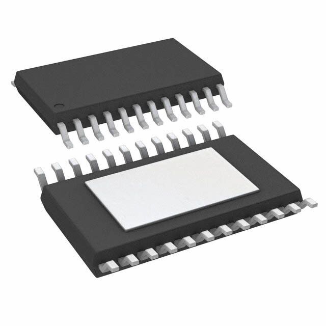
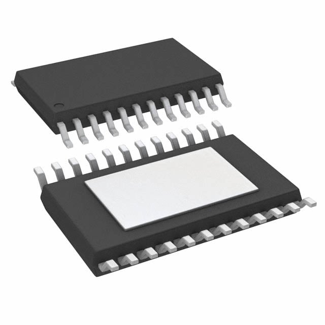
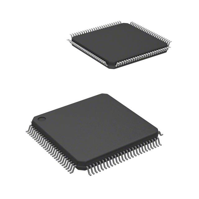
| 描述 | IC PROG HOT SWAP CTRL 24-HTSSOP热交换电压控制器 0-3A 7-15V Sngl Hi-Side MOSFET |
| 产品分类 | |
| 品牌 | Texas Instruments |
| 产品手册 | |
| 产品图片 |
|
| rohs | 符合RoHS无铅 / 符合限制有害物质指令(RoHS)规范要求 |
| 产品系列 | 电源管理 IC,热交换电压控制器,Texas Instruments UCC3915PWP- |
| 数据手册 | http://www.ti.com/lit/pdf/slus198c |
| 产品型号 | UCC3915PWP |
| 产品 | Controllers & Switches |
| 产品目录页面 | |
| 产品种类 | 热交换电压控制器 |
| 供应商器件封装 | 24-HTSSOP |
| 其它名称 | 296-6772-5 |
| 内部开关 | 是 |
| 功能引脚 | B0, B1, B2, B3, CT, /FAULT, IMAX, /SHTDWN, |
| 包装 | 管件 |
| 可编程特性 | 断路器,限流,故障超时 |
| 商标 | Texas Instruments |
| 安装类型 | 表面贴装 |
| 安装风格 | SMD/SMT |
| 封装 | Tube |
| 封装/外壳 | 24-TSSOP(0.173",4.40mm 宽)裸焊盘 |
| 封装/箱体 | TSSOP-24 |
| 工作温度 | 0°C ~ 70°C |
| 工作温度范围 | 0 C to + 70 C |
| 工厂包装数量 | 60 |
| 应用 | 通用 |
| 标准包装 | 60 |
| 特性 | 发热限制 |
| 电压-电源 | 7 V ~ 15 V |
| 电流-电源 | 1mA |
| 电流-输出(最大值) | 4A |
| 电流限制 | 4 A |
| 电源电压-最大 | 15 V |
| 电源电压-最小 | 7 V |
| 电源电流 | 2 mA |
| 类型 | 热交换控制器 |
| 系列 | UCC3915 |
| 输入/电源电压—最大值 | 15 V |
| 输入/电源电压—最小值 | 7 V |
| 通道数 | 1 |
| 通道数量 | 1 Channel |


- 商务部:美国ITC正式对集成电路等产品启动337调查
- 曝三星4nm工艺存在良率问题 高通将骁龙8 Gen1或转产台积电
- 太阳诱电将投资9.5亿元在常州建新厂生产MLCC 预计2023年完工
- 英特尔发布欧洲新工厂建设计划 深化IDM 2.0 战略
- 台积电先进制程称霸业界 有大客户加持明年业绩稳了
- 达到5530亿美元!SIA预计今年全球半导体销售额将创下新高
- 英特尔拟将自动驾驶子公司Mobileye上市 估值或超500亿美元
- 三星加码芯片和SET,合并消费电子和移动部门,撤换高东真等 CEO
- 三星电子宣布重大人事变动 还合并消费电子和移动部门
- 海关总署:前11个月进口集成电路产品价值2.52万亿元 增长14.8%

PDF Datasheet 数据手册内容提取
(cid:26) (cid:1)(cid:2)(cid:2)(cid:3)(cid:4)(cid:5)(cid:6)(cid:7) (cid:1)(cid:2)(cid:2)(cid:9)(cid:4)(cid:5)(cid:6) (cid:5)(cid:6)(cid:10)(cid:11) (cid:12)(cid:13)(cid:14)(cid:15)(cid:13)(cid:16)(cid:17)(cid:17)(cid:16)(cid:18)(cid:19)(cid:20) (cid:21)(cid:14)(cid:22) (cid:23)(cid:24)(cid:16)(cid:12) (cid:12)(cid:14)(cid:24)(cid:20)(cid:13) (cid:17)(cid:16)(cid:25)(cid:16)(cid:15)(cid:20)(cid:13) SLUS198C – FEBUARY 2000 - REVISED - JUNE 2001 (cid:1) Integrated 0.15-Ω Power MOSFET (cid:1) Thermal Shutdown (cid:1) (cid:1) 7-V to 15-V Operation Fault-Output Indicator (cid:1) (cid:1) Digital-Programmable Current Limit from Maximum-Output Current Can Be Set to 1 A 0 A to 3 A Above the Programmed-Fault Level or to a (cid:1) 100-µA I When Disabled Full 4 A CC (cid:1) Programmable On Time (cid:1) Power SOIC and TSSOP, Low Thermal (cid:1) Resistance Packaging Programmable Start Delay (cid:1) Fixed 2% Duty Cycle description The UCC3915 programmable hot swap power manager provides complete power-management, hot-swap capability, and circuit breaker functions. The only external component required to operate the device, other than power supply bypassing, is the fault-timing capacitor, C . All control and housekeeping functions are integrated, T and externally programmable. These include the fault current level, maximum output sourcing current, maximum fault time, and startup delay. In the event of a constant fault, the internal fixed 2% duty cycle ratio limits average output power. The internal 4-bit DAC allows programming of the fault-level current from 0 A to 3 A with 0.25-A resolution. The IMAX control pin sets the maximum-sourcing current to 1 A above the trip level or to a full 4 A of output current for fast output capacitor charging. (continued) block diagram 2 VIN REVERSE VOLTAGE 30 mV H = 4 A CPHUAMRGPE COMPARATOR– + IMAX 10 + VOUT 3 VIN MAX CURRENT SENSE CURRENT 4 A LEVEL H = OPEN + POWER – LINEAR CURRENT FET * 1 A AMPLIFIER ABOVE FAULT 14 VOUT OVER CURRENT COMPARATOR ON TIME CULRERVEENLT 0 –F3A UALT + CONTROL 15 VOUT – 2% DUTY CYCLE THERMAL SHUTDOWN 1.5 V 0–3 A 0.25 INTERNAL + RES BIAS – 1 SHTDWN 6 7 8 9 5 4 13 12 11 16 B3 B2 B1 B0 GND HEAT SINK CT FAULT GND PINS 4 BIT DAC UDG-99174 NOTE: Pin numbers refer to DIL-16 and SOIC-16 packages. Please be aware that an important notice concerning availability, standard warranty, and use in critical applications of TexasInstruments semiconductor products and disclaimers thereto appears at the end of this data sheet. (cid:12)(cid:13)(cid:14)(cid:27)(cid:1)(cid:2)(cid:22)(cid:28)(cid:14)(cid:25) (cid:27)(cid:16)(cid:22)(cid:16) (cid:29)(cid:30)(cid:31) !"#$(cid:29) (cid:30) (cid:29)% &’!!((cid:30)$ #% (cid:31) )’*+(cid:29)&#$(cid:29) (cid:30) ,#$(- Copyright 2000, Texas Instruments Incorporated (cid:12)! ,’&$% & (cid:30)(cid:31) !" $ %)(&(cid:29)(cid:31)(cid:29)&#$(cid:29) (cid:30)% )(! $.( $(!"% (cid:31) (cid:22)(/#% (cid:28)(cid:30)%$!’"((cid:30)$% %$#(cid:30),#!, 0#!!#(cid:30)$1- (cid:12)! ,’&$(cid:29) (cid:30) )! &(%%(cid:29)(cid:30)2 , (% (cid:30) $ (cid:30)(&(%%#!(cid:29)+1 (cid:29)(cid:30)&+’,( $(%$(cid:29)(cid:30)2 (cid:31) #++ )#!#"($(!%- POST OFFICE BOX 655303 • DALLAS, TEXAS 75265 1
(cid:1)(cid:2)(cid:2)(cid:3)(cid:4)(cid:5)(cid:6)(cid:7) (cid:1)(cid:2)(cid:2)(cid:9)(cid:4)(cid:5)(cid:6) (cid:26) (cid:5)(cid:6)(cid:10)(cid:11) (cid:12)(cid:13)(cid:14)(cid:15)(cid:13)(cid:16)(cid:17)(cid:17)(cid:16)(cid:18)(cid:19)(cid:20) (cid:21)(cid:14)(cid:22) (cid:23)(cid:24)(cid:16)(cid:12) (cid:12)(cid:14)(cid:24)(cid:20)(cid:13) (cid:17)(cid:16)(cid:25)(cid:16)(cid:15)(cid:20)(cid:13) SLUS198C – FEBUARY 2000 - REVISED - JUNE 2001 description (continued) When the output current is below the fault level, the output MOSFET is switched on with a nominal ON resistance of 0.15 Ω. When the output current exceeds the fault level, but is less than the maximum-sourcing level, the output remains switched on, but the fault timer starts, charging CT. Once CT charges to a preset threshold, the switch is turned off, and remains off for 50 times the programmed fault time. When the output current reaches the maximum sourcing level, the MOSFET transitions from a switch to a constant current source. The UCC3915 can be put into sleep mode, drawing only 100 µA of supply current. Other features include an open-drain fault-output indicator, thermal shutdown, undervoltage lockout, 7-V to 15-V operation, and low-thermal resistance SOIC and TSSOP power packages. absolute maximum ratings over operating free-air temperature (unless otherwise noted)† VIN . . . . . . . . . . . . . . . . . . . . . . . . . . . . . . . . . . . . . . . . . . . . . . . . . . . . . . . . . . . . . . . . . . . . . . . . . . . . . . . . . . . . 15.5 V VOUT – VIN . . . . . . . . . . . . . . . . . . . . . . . . . . . . . . . . . . . . . . . . . . . . . . . . . . . . . . . . . . . . . . . . . . . . . . . . . . . . . . .0.3 V FAULT sink current . . . . . . . . . . . . . . . . . . . . . . . . . . . . . . . . . . . . . . . . . . . . . . . . . . . . . . . . . . . . . . . . . . . . . . . 50 mA FAULT voltage . . . . . . . . . . . . . . . . . . . . . . . . . . . . . . . . . . . . . . . . . . . . . . . . . . . . . . . . . . . . . . . . . . . . . –0.3 V to 8 V Output current . . . . . . . . . . . . . . . . . . . . . . . . . . . . . . . . . . . . . . . . . . . . . . . . . . . . . . . . . . . . . . . . . . . . . . . Self limiting TTL input voltage . . . . . . . . . . . . . . . . . . . . . . . . . . . . . . . . . . . . . . . . . . . . . . . . . . . . . . . . . . . . . . . . . . . . –0.3 to VIN Storage temperature, T . . . . . . . . . . . . . . . . . . . . . . . . . . . . . . . . . . . . . . . . . . . . . . . . . . . . . . . . . –65°C to 150°C stg Junction temperature, T . . . . . . . . . . . . . . . . . . . . . . . . . . . . . . . . . . . . . . . . . . . . . . . . . . . . . . . . . . –55°C to 150°C J Lead temperature (soldering, 10 sec.) . . . . . . . . . . . . . . . . . . . . . . . . . . . . . . . . . . . . . . . . . . . . . . . . . . . . . . 300°C †Stresses beyond those listed under “absolute maximum ratings” may cause permanent damage to the device. These are stress ratings only, and functional operation of the device at these or any other conditions beyond those indicated under “recommended operating conditions” is not implied. Exposure to absolute-maximum-rated conditions for extended periods may affect device reliability. ‡Currents are positive into, negative out of the specified terminal. Consult Packaging Section of the Interface Products Data Book (TI Literature Number SLUD002) for thermal limitations and considerations of packages. package information DIL-16, SOIC-16 TSSOP-24, N, DP Package PWP Package (TOP VIEW) (TOP VIEW) SHTDWN 1 24 FAULT SHTDWN 1 16 FAULT VIN 2 23 VOUT VIN 2 15 VOUT VIN 3 22 VOUT VIN 3 14 VOUT N/C 4 21 N/C GND* 5 20 GND* GND* 4 13 GND* GND* 6 19 GND* EGND* 5 12 GND* GND* 7 18 GND* GND* 8 17 GND* B3 6 11 CT EGND* 9 16 N/C B2 7 10 IMAX B3 10 15 CT B1 8 9 B0 B2 11 14 IMAX B1 12 13 B0 *Pin 5 serves as lowest impedance to the electrical *Pin 9 serves as lowest impedance to the electrical ground; ground; Pins 4, 12, and 13 serve as heat sink/ground. other GND pins serve as heat sink/ground. These pins should These pins should be connected to large etch areas to be connected to large etch areas to help dissipate heat. help dissipate heat. For N Package, pins 4, 12, and 13 are N/C. 2 POST OFFICE BOX 655303 • DALLAS, TEXAS 75265
(cid:26) (cid:1)(cid:2)(cid:2)(cid:3)(cid:4)(cid:5)(cid:6)(cid:7) (cid:1)(cid:2)(cid:2)(cid:9)(cid:4)(cid:5)(cid:6) (cid:5)(cid:6)(cid:10)(cid:11) (cid:12)(cid:13)(cid:14)(cid:15)(cid:13)(cid:16)(cid:17)(cid:17)(cid:16)(cid:18)(cid:19)(cid:20) (cid:21)(cid:14)(cid:22) (cid:23)(cid:24)(cid:16)(cid:12) (cid:12)(cid:14)(cid:24)(cid:20)(cid:13) (cid:17)(cid:16)(cid:25)(cid:16)(cid:15)(cid:20)(cid:13) SLUS198C – FEBUARY 2000 - REVISED - JUNE 2001 electrical characteristics, these specifications apply for T = –40°C to 85°C for the UCC2915 and A 0°C to 70°C for the UCC3915, VIN = 12 V, IMAX = 0.4 V, SHTDWN = 2.4 V, T = T , (unless otherwise A J stated) supply PARAMETER TEST CONDITIONS MIN TYP MAX UNITS Voltage input range 7.0 15.0 V Supply current 1.0 2.0 mA Sleep mode current SHTDWN = 0.2 V, no load 100 150 µA Output leakage SHTDWN = 0.2 V 20 µA NOTE 1: All voltages are with respect to GND. Current is positive into and negative out of the specified terminal. output PARAMETER TEST CONDITIONS MIN TYP MAX UNITS IOUT = 1 A (10 V to 12 V) 0.15 0.3 V IOUT = 2 A (10 V to 12 V) 0.3 0.6 V IOUT = 3 A (10 V to 12 V) 0.45 0.9 V VVoollttaaggee ddrroopp IOUT = 1 A, VIN = 7 V and 15 V 0.2 0.4 V IOUT = 2 A, VIN = 7 V and 15 V 0.4 0.8 V IOUT = 3 A, VIN = 7 V, 12 V MAX 0.6 1.2 V Initial startup time See Note 2 100 µs Short circuit response See Note 2 100 ns Thermal shutdown See Note 2 165 °C Thermal hysteresis See Note 2 10 °C NOTE 1: All voltages are with respect to GND. Current is positive into and negative out of the specified terminal. NOTE 2: Ensured by design. Not production tested. DAC PARAMETER TEST CONDITIONS MIN TYP MAX UNITS Code = 0000–0011 (device off) Code = 0100 0.07 0.25 0.45 A Code = 0101 0.32 0.50 0.70 A Code = 0110 0.50 0.75 0.98 A Code = 0111 0.75 1.00 1.3 A TTrriip ccuurrrreenntt Code = 1000 1.0 1.25 1.6 A Code = 1001 1.25 1.50 1.85 A Code = 1010 1.5 1.75 2.15 A Code = 1011 1.70 2.00 2.4 A Code = 1100 1.90 2.25 2.7 A Code = 1101 2.1 2.50 2.95 A NOTE 1: All voltages are with respect to GND. Current is positive into and negative out of the specified terminal. POST OFFICE BOX 655303 • DALLAS, TEXAS 75265 3
(cid:1)(cid:2)(cid:2)(cid:3)(cid:4)(cid:5)(cid:6)(cid:7) (cid:1)(cid:2)(cid:2)(cid:9)(cid:4)(cid:5)(cid:6) (cid:26) (cid:5)(cid:6)(cid:10)(cid:11) (cid:12)(cid:13)(cid:14)(cid:15)(cid:13)(cid:16)(cid:17)(cid:17)(cid:16)(cid:18)(cid:19)(cid:20) (cid:21)(cid:14)(cid:22) (cid:23)(cid:24)(cid:16)(cid:12) (cid:12)(cid:14)(cid:24)(cid:20)(cid:13) (cid:17)(cid:16)(cid:25)(cid:16)(cid:15)(cid:20)(cid:13) SLUS198C – FEBUARY 2000 - REVISED - JUNE 2001 electrical characteristics, these specifications apply for T = –40°C to 85°C for the UCC2915 and A 0°C to 70°C for the UCC3915, VIN = 12 V, IMAX = 0.4 V, SHTDWN = 2.4 V, T = T , (unless otherwise A J stated) DAC (continued) PARAMETER TEST CONDITIONS MIN TYP MAX UNITS Code = 1110 2.30 2.75 3.25 A TTrriipp ccurrrreenntt Code = 1111 2.50 3.0 3.50 A Max output current over trip (current source mode) Code = 0100 to 1111, IMAX = 0 V 0.35 1.0 1.65 A Max output current (current source mode) Code = 0100 to 1111, IMAX = 2.4 V 3.0 4.0 5.2 A NOTE 1: All voltages are with respect to GND. Current is positive into and negative out of the specified terminal. fault timer PARAMETER TEST CONDITIONS MIN TYP MAX UNITS CT charge current VCT = 1.0 V –83 –62 –47 µA CT discharge current VCT = 1.0 V 0.8 1.2 1.8 µA Output duty cycle VOUT = 0 V 1.0% 1.9% 3.3% CT fault threshold 1.2 1.5 1.7 V CT reset threshold 0.4 0.5 0.6 V NOTE 1: All voltages are with respect to GND. Current is positive into and negative out of the specified terminal. shutdown PARAMETER TEST CONDITIONS MIN TYP MAX UNITS Shutdown threshold 1.1 1.5 1.9 V Shutdown hysteresis 150 mV Input current 100 500 nA NOTE 1: All voltages are with respect to GND. Current is positive into and negative out of the specified terminal. open drain output (FAULT) PARAMETER TEST CONDITIONS MIN TYP MAX UNITS High level output current FAULT = 5 V 250 µA Low level output voltage IOUT = 5 mA 0.2 0.8 V NOTE 1: All voltages are with respect to GND. Current is positive into and negative out of the specified terminal. TTL input dc characteristics PARAMETER TEST CONDITIONS MIN TYP MAX UNITS TTL input voltage high 2.0 V TTL input voltage low 0.8 V TTL input high current VIH = 2.4 V 3 10 µA TTL input low current VIL = 0.4 V 1 µA NOTE 1: All voltages are with respect to GND. Current is positive into and negative out of the specified terminal. 4 POST OFFICE BOX 655303 • DALLAS, TEXAS 75265
(cid:26) (cid:1)(cid:2)(cid:2)(cid:3)(cid:4)(cid:5)(cid:6)(cid:7) (cid:1)(cid:2)(cid:2)(cid:9)(cid:4)(cid:5)(cid:6) (cid:5)(cid:6)(cid:10)(cid:11) (cid:12)(cid:13)(cid:14)(cid:15)(cid:13)(cid:16)(cid:17)(cid:17)(cid:16)(cid:18)(cid:19)(cid:20) (cid:21)(cid:14)(cid:22) (cid:23)(cid:24)(cid:16)(cid:12) (cid:12)(cid:14)(cid:24)(cid:20)(cid:13) (cid:17)(cid:16)(cid:25)(cid:16)(cid:15)(cid:20)(cid:13) SLUS198C – FEBUARY 2000 - REVISED - JUNE 2001 pin descriptions B0 – B3: These pins provide digital input to the DAC, which sets the fault-current threshold. They can be used to provide a digital soft-start and adaptive-current limiting. CT: A capacitor connected to ground sets the maximum-fault time. The maximum-fault time must be more than the time required to charge the external capacitance in one cycle. The maximum-fault time is defined as T = 16.1 × 10³ × C . Once the fault time is reached the output will shutdown for a time given by FAULT T T = 833× 103 × C , this equates to a 1.9% duty cycle. SD T FAULT: Open-drain output, which pulls low upon any fault or interrupt condition, or thermal shutdown. IMAX: When this pin is set to a logic low, the maximum-sourcing current will always be 1 A above the programmed-fault level. When set to a logic high, the maximum-sourcing current will be a constant 4 A for applications which require fast charging of load capacitance. SHTDWN: When this pin is brought to a logic low, the IC is put into a sleep mode drawing typically less than 100 µA of I .The input threshold is hysteretic, allowing the user to program a startup delay with an external CC RC circuit. VIN: Input voltage to the UCC3915. The recommended voltage range is 7 V to 15 V. Both VIN pins should be connected together and connected to the power source. VOUT: Output voltage from the UCC3915. Both VOUT pins should be connected together and connected to the load. When switched the output voltage will be approximately V – (0.15 Ω × I ). VOUT must not exceed IN OUT VIN by greater than 0.3 V. APPLICATION INFORMATION 4 12 13 5 V IN HEAT SINK GND V 2 GND PINS OUT 14 VIN C VOUT IN 3 R D1 L C 15 OUT UCC3915 RSD VIN S6 5 V R1 LED SHTDWN 1 16 FAULT C SD 11 CT B3 B2 B1 B0 IMAX 6 7 8 9 10 C T V IN DIP S1 S2 S3 S4 S5 SWITCH UDG-99175 Figure 1. Evaluation Circuit POST OFFICE BOX 655303 • DALLAS, TEXAS 75265 5
(cid:1)(cid:2)(cid:2)(cid:3)(cid:4)(cid:5)(cid:6)(cid:7) (cid:1)(cid:2)(cid:2)(cid:9)(cid:4)(cid:5)(cid:6) (cid:26) (cid:5)(cid:6)(cid:10)(cid:11) (cid:12)(cid:13)(cid:14)(cid:15)(cid:13)(cid:16)(cid:17)(cid:17)(cid:16)(cid:18)(cid:19)(cid:20) (cid:21)(cid:14)(cid:22) (cid:23)(cid:24)(cid:16)(cid:12) (cid:12)(cid:14)(cid:24)(cid:20)(cid:13) (cid:17)(cid:16)(cid:25)(cid:16)(cid:15)(cid:20)(cid:13) SLUS198C – FEBUARY 2000 - REVISED - JUNE 2001 APPLICATION INFORMATION protecting the UCC3915 from voltage transients The parasitic inductance associated with the power distribution can cause a voltage spike at V if the load IN current is suddenly interrupted by the UCC3915. It is important to limit the peak of this spike to less than 15 V to prevent damage to the UCC3915. This voltage spike can be minimized by: (cid:1) Reducing the power distribution inductance (e.g., twist the positive (+) and negative (–) leads of the power supply feeding V , locate the power supply close to the UCC3915 or use PCB power and ground planes). IN (cid:1) Decoupling V with a capacitor, C (refer to Figure 1), located close to the V pins. This capacitor is IN IN IN typically 1 µF or less to limit the inrush current. (cid:1) Clamping the voltage at V below 15 V with a Zener diode, D1(refer to Figure 1), located close to the V IN IN pins. Figure 2. Load Current, Timing-Capacitor Voltage, and Output Voltage of the UCC3915 Under Fault Conditions estimating maximum load capacitance For hot-swap applications, the rate at which the total output capacitance can be charged depends on the maximum-output current available and the nature of the load. For a constant-current, current-limited application, the output will come up if the load asks for less than the maximum available short-circuit current. To ensure recovery of a duty cycle from a short-circuited load condition, there is a maximum total output capacitance which can be charged for a given unit on time (fault time). The design value of on or fault time can be adjusted by changing the timing capacitor C . T 6 POST OFFICE BOX 655303 • DALLAS, TEXAS 75265
(cid:26) (cid:1)(cid:2)(cid:2)(cid:3)(cid:4)(cid:5)(cid:6)(cid:7) (cid:1)(cid:2)(cid:2)(cid:9)(cid:4)(cid:5)(cid:6) (cid:5)(cid:6)(cid:10)(cid:11) (cid:12)(cid:13)(cid:14)(cid:15)(cid:13)(cid:16)(cid:17)(cid:17)(cid:16)(cid:18)(cid:19)(cid:20) (cid:21)(cid:14)(cid:22) (cid:23)(cid:24)(cid:16)(cid:12) (cid:12)(cid:14)(cid:24)(cid:20)(cid:13) (cid:17)(cid:16)(cid:25)(cid:16)(cid:15)(cid:20)(cid:13) SLUS198C – FEBUARY 2000 - REVISED - JUNE 2001 APPLICATION INFORMATION For worst-case constant-current load of value just less than the trip limit; C can be estimated from: OUT(max) (cid:2) (cid:4) (cid:2) (cid:4) 16.1(cid:5)103(cid:5)C C (cid:1) I (cid:3)I (cid:5) T OUT(max) MAX LOAD V OUT Where V is the output voltage. OUT For a resistive load of value R , the value of C can be estimated from: L OUT(max) (cid:7) (cid:14) (cid:6) (cid:6) (cid:6) (cid:6) (cid:6) (cid:6) (cid:6) (cid:6) (cid:6) (cid:6) (cid:6) 16.1(cid:5)103(cid:5)C (cid:6) C (cid:1)(cid:6) T (cid:6) OUT(max) (cid:10) (cid:12) (cid:6) (cid:6) (cid:6) (cid:6) (cid:6) (cid:6)(cid:6) (cid:6)(cid:6)(cid:6) (cid:6)R (cid:5)(cid:9)n(cid:6) 1 (cid:6)(cid:6) L V OUT (cid:8) (cid:11)1(cid:3)I (cid:5)R (cid:13)(cid:15) MAX L Long C times must consider the maximum temperature. Thermal shutdown protection may be the limiting fault T time. safety recommendations Although the UCC3915 is designed to provide system protection for all fault conditions, all integrated circuits can ultimately fail short. For this reason, if the UCC3915 is intended for use in safety-critical applications where UL or some other safety rating is required, a redundant safety device such as a fuse should be placed in series with the device. The UCC3915 will prevent the fuse from blowing for virtually all fault conditions, increasing system reliability and reducing maintenance cost, in addition to providing the hot-swap benefits of the device. POST OFFICE BOX 655303 • DALLAS, TEXAS 75265 7
PACKAGE OPTION ADDENDUM www.ti.com 6-Feb-2020 PACKAGING INFORMATION Orderable Device Status Package Type Package Pins Package Eco Plan Lead/Ball Finish MSL Peak Temp Op Temp (°C) Device Marking Samples (1) Drawing Qty (2) (6) (3) (4/5) UCC2915DP ACTIVE SOIC D 16 40 Green (RoHS NIPDAU Level-2-260C-1 YEAR -40 to 85 UCC2915DP & no Sb/Br) UCC3915DP ACTIVE SOIC D 16 40 Green (RoHS NIPDAU Level-2-260C-1 YEAR 0 to 70 UCC3915DP & no Sb/Br) UCC3915DPG4 ACTIVE SOIC D 16 40 Green (RoHS NIPDAU Level-2-260C-1 YEAR 0 to 70 UCC3915DP & no Sb/Br) UCC3915DPTR ACTIVE SOIC D 16 2500 Green (RoHS NIPDAU Level-2-260C-1 YEAR 0 to 70 UCC3915DP & no Sb/Br) (1) The marketing status values are defined as follows: ACTIVE: Product device recommended for new designs. LIFEBUY: TI has announced that the device will be discontinued, and a lifetime-buy period is in effect. NRND: Not recommended for new designs. Device is in production to support existing customers, but TI does not recommend using this part in a new design. PREVIEW: Device has been announced but is not in production. Samples may or may not be available. OBSOLETE: TI has discontinued the production of the device. (2) RoHS: TI defines "RoHS" to mean semiconductor products that are compliant with the current EU RoHS requirements for all 10 RoHS substances, including the requirement that RoHS substance do not exceed 0.1% by weight in homogeneous materials. Where designed to be soldered at high temperatures, "RoHS" products are suitable for use in specified lead-free processes. TI may reference these types of products as "Pb-Free". RoHS Exempt: TI defines "RoHS Exempt" to mean products that contain lead but are compliant with EU RoHS pursuant to a specific EU RoHS exemption. Green: TI defines "Green" to mean the content of Chlorine (Cl) and Bromine (Br) based flame retardants meet JS709B low halogen requirements of <=1000ppm threshold. Antimony trioxide based flame retardants must also meet the <=1000ppm threshold requirement. (3) MSL, Peak Temp. - The Moisture Sensitivity Level rating according to the JEDEC industry standard classifications, and peak solder temperature. (4) There may be additional marking, which relates to the logo, the lot trace code information, or the environmental category on the device. (5) Multiple Device Markings will be inside parentheses. Only one Device Marking contained in parentheses and separated by a "~" will appear on a device. If a line is indented then it is a continuation of the previous line and the two combined represent the entire Device Marking for that device. (6) Lead/Ball Finish - Orderable Devices may have multiple material finish options. Finish options are separated by a vertical ruled line. Lead/Ball Finish values may wrap to two lines if the finish value exceeds the maximum column width. Important Information and Disclaimer:The information provided on this page represents TI's knowledge and belief as of the date that it is provided. TI bases its knowledge and belief on information provided by third parties, and makes no representation or warranty as to the accuracy of such information. Efforts are underway to better integrate information from third parties. TI has taken and Addendum-Page 1
PACKAGE OPTION ADDENDUM www.ti.com 6-Feb-2020 continues to take reasonable steps to provide representative and accurate information but may not have conducted destructive testing or chemical analysis on incoming materials and chemicals. TI and TI suppliers consider certain information to be proprietary, and thus CAS numbers and other limited information may not be available for release. In no event shall TI's liability arising out of such information exceed the total purchase price of the TI part(s) at issue in this document sold by TI to Customer on an annual basis. Addendum-Page 2
PACKAGE MATERIALS INFORMATION www.ti.com 15-Sep-2018 TAPE AND REEL INFORMATION *Alldimensionsarenominal Device Package Package Pins SPQ Reel Reel A0 B0 K0 P1 W Pin1 Type Drawing Diameter Width (mm) (mm) (mm) (mm) (mm) Quadrant (mm) W1(mm) UCC3915DPTR SOIC D 16 2500 330.0 16.4 6.5 10.3 2.1 8.0 16.0 Q1 PackMaterials-Page1
PACKAGE MATERIALS INFORMATION www.ti.com 15-Sep-2018 *Alldimensionsarenominal Device PackageType PackageDrawing Pins SPQ Length(mm) Width(mm) Height(mm) UCC3915DPTR SOIC D 16 2500 367.0 367.0 38.0 PackMaterials-Page2
GENERIC PACKAGE VIEW PWP 24 PowerPADTM TSSOP - 1.2 mm max height 4.4 x 7.6, 0.65 mm pitch PLASTIC SMALL OUTLINE This image is a representation of the package family, actual package may vary. Refer to the product data sheet for package details. 4224742/B www.ti.com
None
None
IMPORTANTNOTICEANDDISCLAIMER TI PROVIDES TECHNICAL AND RELIABILITY DATA (INCLUDING DATASHEETS), DESIGN RESOURCES (INCLUDING REFERENCE DESIGNS), APPLICATION OR OTHER DESIGN ADVICE, WEB TOOLS, SAFETY INFORMATION, AND OTHER RESOURCES “AS IS” AND WITH ALL FAULTS, AND DISCLAIMS ALL WARRANTIES, EXPRESS AND IMPLIED, INCLUDING WITHOUT LIMITATION ANY IMPLIED WARRANTIES OF MERCHANTABILITY, FITNESS FOR A PARTICULAR PURPOSE OR NON-INFRINGEMENT OF THIRD PARTY INTELLECTUAL PROPERTY RIGHTS. These resources are intended for skilled developers designing with TI products. You are solely responsible for (1) selecting the appropriate TI products for your application, (2) designing, validating and testing your application, and (3) ensuring your application meets applicable standards, and any other safety, security, or other requirements. These resources are subject to change without notice. TI grants you permission to use these resources only for development of an application that uses the TI products described in the resource. Other reproduction and display of these resources is prohibited. No license is granted to any other TI intellectual property right or to any third party intellectual property right. TI disclaims responsibility for, and you will fully indemnify TI and its representatives against, any claims, damages, costs, losses, and liabilities arising out of your use of these resources. TI’s products are provided subject to TI’s Terms of Sale (www.ti.com/legal/termsofsale.html) or other applicable terms available either on ti.com or provided in conjunction with such TI products. TI’s provision of these resources does not expand or otherwise alter TI’s applicable warranties or warranty disclaimers for TI products. Mailing Address: Texas Instruments, Post Office Box 655303, Dallas, Texas 75265 Copyright © 2020, Texas Instruments Incorporated