ICGOO在线商城 > 集成电路(IC) > 线性 - 音頻放大器 > LM4941TM/NOPB

 Datasheet下载
- 型号: LM4941TM/NOPB
- 制造商: Texas Instruments
- 库位|库存: xxxx|xxxx
- 要求:
| 数量阶梯 | 香港交货 | 国内含税 |
| +xxxx | $xxxx | ¥xxxx |
查看当月历史价格
查看今年历史价格
LM4941TM/NOPB产品简介:
ICGOO电子元器件商城为您提供LM4941TM/NOPB由Texas Instruments设计生产,在icgoo商城现货销售,并且可以通过原厂、代理商等渠道进行代购。 LM4941TM/NOPB价格参考。Texas InstrumentsLM4941TM/NOPB封装/规格:线性 - 音頻放大器, Amplifier IC 1-Channel (Mono) Class AB 9-µSMD (1.25x1.25)。您可以下载LM4941TM/NOPB参考资料、Datasheet数据手册功能说明书,资料中有LM4941TM/NOPB 详细功能的应用电路图电压和使用方法及教程。
LM4941TM/NOPB 是 Texas Instruments(德州仪器)生产的一款音频功率放大器,属于 D 类音频放大器。它主要用于便携式音频设备中,适用于需要高效能、低功耗、小尺寸的音频放大应用场景。

该芯片常用于以下场景:

1. 便携式音频设备:如 MP3 播放器、便携式收音机、蓝牙音箱等,因其高效率和低功耗特性,适合电池供电设备使用。

2. 手机与智能设备:用于智能手机、平板电脑等设备的扬声器驱动,提供清晰的音频输出,同时减少对电池的消耗。

3. 小型音响系统:如桌面音响、便携式扩音器等,提供高质量音频放大输出。

4. 车载音频系统:用于车载娱乐系统中的音频放大,满足车内有限空间和电源限制下的音频需求。

该芯片采用 16 引脚 TSSOP 封装,具备过热保护、过流保护等功能,增强了系统的稳定性和可靠性。其无需输出滤波器的设计也简化了外围电路,降低了设计复杂度和成本。

总之,LM4941TM/NOPB 广泛应用于对音质、效率和体积有较高要求的便携式或低功耗音频设备中。
| 参数 | 数值 |
| 产品目录 | 集成电路 (IC)半导体 |
| 描述 | IC AMP AUDIO PWR 1.54W AB 9DSBGA音频放大器 1.25 Watt Fully Differential Audio Power Amplifier With RF Suppression and Shutdown 9-DSBGA -40 to 85 |
| 产品分类 | |
| 品牌 | Texas Instruments |
| 产品手册 | http://www.ti.com/litv/snas347c |
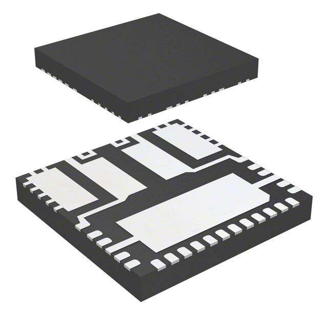
| 产品图片 |
|
| rohs | 符合RoHS无铅 / 符合限制有害物质指令(RoHS)规范要求 |
| 产品系列 | 音频 IC,音频放大器,Texas Instruments LM4941TM/NOPBBoomer®, PowerWise® |
| 数据手册 | |
| 产品型号 | LM4941TM/NOPB |
| PCN组件/产地 | |
| THD+噪声 | 0.04 % |
| 不同负载时的最大输出功率x通道数 | 1.54W x 1 @ 8 欧姆 |
| 产品 | Class-AB |
| 产品目录页面 | |
| 产品种类 | 音频放大器 |
| 供应商器件封装 | 9-DSBGA |
| 其它名称 | *LM4941TM/NOPB |
| 包装 | 剪切带 (CT) |
| 商标 | Texas Instruments |
| 安装类型 | 表面贴装 |
| 安装风格 | SMD/SMT |
| 封装 | Reel |
| 封装/外壳 | 9-WFBGA |
| 封装/箱体 | DSBGA-9 |
| 工作温度 | -40°C ~ 85°C (TA) |
| 工作电源电压 | 2.4 V to 5.5 V |
| 工厂包装数量 | 250 |
| 最小工作温度 | - 40 C |
| 标准包装 | 1 |
| 特性 | 消除爆音,差分输入,关闭,热保护 |
| 电压-电源 | 2.4 V ~ 5.5 V |
| 电源电压-最大 | 5.5 V |
| 电源电压-最小 | 2.4 V |
| 电源电流 | 1.7 mA |
| 电源类型 | Single |
| 类型 | Audio Power Amplifier |
| 系列 | LM4941 |
| 输出功率 | 1.54 W |
| 输出类型 | 1-通道(单声道) |
| 配用 | /product-detail/zh/LM4941TMBD/LM4941TMBD-ND/1640777 |


PDF Datasheet 数据手册内容提取
LM4941, LM4941SDBD, LM4941TMBD www.ti.com SNAS347C–JUNE2006–REVISEDMAY2013 LM4941 1.25 Watt Fully Differential Audio Power Amplifier With RF Suppression and Shutdown CheckforSamples:LM4941,LM4941SDBD,LM4941TMBD FEATURES DESCRIPTION 1 • ImprovedRFSuppression,ByUpto20dB The LM4941 is a fully differential audio power 2 amplifier primarily designed for demanding OverPreviousDesignsinSelected applications in mobile phones and other portable Applications communication device applications. It is capable of • FullyDifferentialAmplification delivering 1.25 watts of continuous average power to • AvailableinSpace-SavingDSBGAPackage a 8Ω load with less than 1% distortion (THD+N) from a 5V power supply. The LM4941 does not require • UltraLowCurrentShutdownMode DC output coupling capacitors or bootstrap capacitors, • CanDriveCapacitiveLoadsupto100pF and therefore is ideally suited for mobile phone and • ImprovedPop&ClickCircuitryEliminates other small form factor applications where minimal NoisesDuringTurn-OnandTurn-Off PCBspaceisaprimaryrequirement. Transitions The LM4941 also features proprietary internal • 2.4-5.5VOperation circuitry that suppresses the coupling of RF signals • NoOutputCouplingCapacitors,Snubber into the chip. This is important because certain types of RF signals (such as GSM) can couple into audio NetworksorBootstrapCapacitorsRequired amplifiers in such a way that part of the signal is heard through the speaker. The RF suppression APPLICATIONS circuitry in the LM4941 makes it well-suited for • MobilePhones portable applications in which strong RF signals generated by an antenna from or a cellular phone or • PDAs other portable electronic device may couple audibly • PortableElectronicDevices intotheamplifier. KEY SPECIFICATIONS Other features include a low-power consumption shutdown mode, internal thermal shutdown • ImprovedPSRRat217Hz95dB(typ) protection,andadvancedpop&clickcircuitry. • PowerOutput,V =5.0V,R =8Ω,1%THD+N DD L 1.25W(typ) • PowerOutput,V =3.0V,R =8Ω,1%THD+N DD L 430mW(typ) • ShutdownCurrent0.1µA(typ) 1 Pleasebeawarethatanimportantnoticeconcerningavailability,standardwarranty,anduseincriticalapplicationsof TexasInstrumentssemiconductorproductsanddisclaimerstheretoappearsattheendofthisdatasheet. Alltrademarksarethepropertyoftheirrespectiveowners. 2 PRODUCTIONDATAinformationiscurrentasofpublicationdate. Copyright©2006–2013,TexasInstrumentsIncorporated Products conform to specifications per the terms of the Texas Instruments standard warranty. Production processing does not necessarilyincludetestingofallparameters.
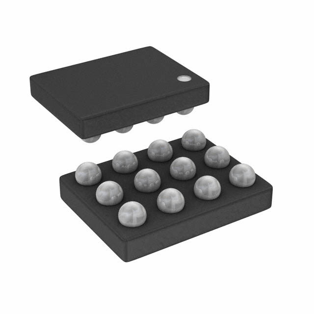
LM4941, LM4941SDBD, LM4941TMBD SNAS347C–JUNE2006–REVISEDMAY2013 www.ti.com Typical Application VDD + CS RF1 1 PF 20 k: Ri1 - Differential Input 20 k: -IN - + VO+ SHUTDOWN Bias CMoomdemon R8:L VO- - 1.0 PF CB BYP + Differential Input Ri2 +IN + 20 k: GND RF2 20 k: Figure1. TypicalAudioAmplifierApplicationCircuit Connection Diagram xxx xxx 3 OUT- VDD OUT+ -IN 1 8 OUT+ BYP 2 7 VDD 2 +IN GND -IN SHDN 3 6 GND +IN 4 5 OUT- 1 SHDN GND BYP Figure3. 8-PinWSON-TopView A B C SeeNGS0008CPackage Figure2. 9-BumpDSBGA-TopView SeeYFQ0009Package Thesedeviceshavelimitedbuilt-inESDprotection.Theleadsshouldbeshortedtogetherorthedeviceplacedinconductivefoam duringstorageorhandlingtopreventelectrostaticdamagetotheMOSgates. 2 SubmitDocumentationFeedback Copyright©2006–2013,TexasInstrumentsIncorporated ProductFolderLinks:LM4941 LM4941SDBD LM4941TMBD
LM4941, LM4941SDBD, LM4941TMBD www.ti.com SNAS347C–JUNE2006–REVISEDMAY2013 Absolute Maximum Ratings(1)(2)(3) SupplyVoltage 6.0V StorageTemperature −65°Cto+150°C InputVoltage −0.3VtoV +0.3V DD PowerDissipation(4)(5) InternallyLimited ESDSusceptibility(6) 2000V ESDSusceptibility(7) 200V JunctionTemperature 150°C ThermalResistance θ (TM) 100°C/W JA θ (WSON) 71°C/W JA SolderingInformation SeeAN-1187(SNOA401) (1) Allvoltagesaremeasuredwithrespecttothegroundpin,unlessotherwisespecified. (2) AbsoluteMaximumRatingsindicatelimitsbeyondwhichdamagetothedevicemayoccur.OperatingRatingsindicateconditionsfor whichthedeviceisfunctional,butdonotensurespecificperformancelimits.ElectricalCharacteristicsstateDCandACelectrical specificationsunderparticulartestconditionswhichensurespecificperformancelimits.Thisassumesthatthedeviceiswithinthe OperatingRatings.Specificationsarenotensuredforparameterswherenolimitisgiven,however,thetypicalvalueisagoodindication ofdeviceperformance. (3) IfMilitary/Aerospacespecifieddevicesarerequired,pleasecontacttheTISalesOffice/Distributorsforavailabilityandspecifications. (4) ThemaximumpowerdissipationmustbederatedatelevatedtemperaturesandisdictatedbyT ,θ ,andtheambienttemperature JMAX JA T .ThemaximumallowablepowerdissipationisP =(T –T )/θ orthenumbergiveninAbsoluteMaximumRatings, A DMAX JMAX A JA whicheverislower.FortheLM4941,seepowerderatingcurveforadditionalinformation. (5) MaximumPowerDissipation(P )inthedeviceoccursatanoutputpowerlevelsignificantlybelowfulloutputpower.P canbe DMAX DMAX calculatedusingEquation3shownintheApplicationsection.ItmayalsobeobtainedfromthePowerDissipationgraphs. (6) Humanbodymodel,100pFdischargedthrougha1.5kΩresistor. (7) MachineModel,220pF–240pFdischargedthroughallpins. Operating Ratings TemperatureRangeT ≤T ≤T −40°C≤T ≤85°C MIN A MAX A SupplyVoltage 2.4V≤V ≤5.5V DD Electrical Characteristics V = 5V(1)(2) DD ThefollowingspecificationsapplyforV =5V,A =1V/V,and8Ωloadunlessotherwisespecified.LimitsapplyforT = DD V A 25°C. LM4941 Units Symbol Parameter Conditions Typical(3) Limit(4)(5) (Limits) V =0V,noload 1.7 2.3 mA(max) I QuiescentPowerSupplyCurrent IN DD V =0V,R =8Ω 1.7 mA IN L I ShutdownCurrent V =GND 0.1 0.8 µA(max) SD SHDN THD+N=1%(max);f=1kHz R =8Ω 1.25 1.15 W(min) L P OutputPower O THD+N=10%(max);f=1kHz R =8Ω 1.54 W L THD+N TotalHarmonicDistortion+Noise P =0.7W;f=1kHz 0.04 % O V =200mV Sine RIPPLE P-P PSRR PowerSupplyRejectionRatio f=217Hz(6) 95 80 dB(min) f=1kHz(6) 90 dB (1) Allvoltagesaremeasuredwithrespecttothegroundpin,unlessotherwisespecified. (2) AbsoluteMaximumRatingsindicatelimitsbeyondwhichdamagetothedevicemayoccur.OperatingRatingsindicateconditionsfor whichthedeviceisfunctional,butdonotensurespecificperformancelimits.ElectricalCharacteristicsstateDCandACelectrical specificationsunderparticulartestconditionswhichensurespecificperformancelimits.Thisassumesthatthedeviceiswithinthe OperatingRatings.Specificationsarenotensuredforparameterswherenolimitisgiven,however,thetypicalvalueisagoodindication ofdeviceperformance. (3) Typicalsaremeasuredat25°Candrepresenttheparametricnorm. (4) LimitsarespecifiedtoTI'sAOQL(AverageOutgoingQualityLevel). (5) Datasheetmin/maxspecificationlimitsarespecifiedbydesign,test,orstatisticalanalysis. (6) 10Ωterminatedinput. Copyright©2006–2013,TexasInstrumentsIncorporated SubmitDocumentationFeedback 3 ProductFolderLinks:LM4941 LM4941SDBD LM4941TMBD
LM4941, LM4941SDBD, LM4941TMBD SNAS347C–JUNE2006–REVISEDMAY2013 www.ti.com Electrical Characteristics V = 5V(1)(2) (continued) DD ThefollowingspecificationsapplyforV =5V,A =1V/V,and8Ωloadunlessotherwisespecified.LimitsapplyforT = DD V A 25°C. LM4941 Units Symbol Parameter Conditions Typical(3) Limit(4)(5) (Limits) f=217Hz,V =200mV Sine 70 dB CM P-P CMRR Common-ModeRejectionRatio f=20Hz–20kHz,V =200mV 70 dB CM pp V OutputOffsetVoltage V =0V 2 6 mV(max) OS IN V ShutdownVoltageInputHigh 1.4 V(min) SDIH V ShutdownVoltageInputLow 0.4 V(max) SDIL SNR Signal-to-NoiseRatio P =1W,f=1kHz 108 dB O T Wake-upTimefromShutdown C =1μF 12 ms WU BYPASS Electrical Characteristics V = 3V(1)(2) DD ThefollowingspecificationsapplyforV =3V,A =1V/V,and8Ωloadunlessotherwisespecified.LimitsapplyforT = DD V A 25°C. LM4941 Units Symbol Parameter Conditions Typical(3) Limit(4)(5) (Limits) V =0V,noload 1.6 2.2 mA(max) I QuiescentPowerSupplyCurrent IN DD V =0V,R =8Ω 1.6 mA IN L I ShutdownCurrent V =GND 0.1 0.8 µA(max) SD SHDN THD+N=1%(max);f=1kHz R =8Ω 0.43 W L P OutputPower O THD+N=10%(max);f=1kHz R =8Ω 0.54 W L THD+N TotalHarmonicDistortion+Noise P =0.25W;f=1kHz 0.05 % O V =200mV Sine RIPPLE PP PSRR PowerSupplyRejectionRatio f=217Hz(6) 95 dB f=1kHz(6) 90 dB CMRR Common-ModeRejectionRatio f=217Hz,V =200mV Sine 70 dB CM PP V OutputOffsetVoltage V =0V 2 6 mV(max) OS IN V ShutdownVoltageInputHigh 1.4 V(min) SDIH V ShutdownVoltageInputLow 0.4 V(max) SDIL T Wake-upTimefromShutdown C =1μF 8 ms WU BYPASS (1) Allvoltagesaremeasuredwithrespecttothegroundpin,unlessotherwisespecified. (2) AbsoluteMaximumRatingsindicatelimitsbeyondwhichdamagetothedevicemayoccur.OperatingRatingsindicateconditionsfor whichthedeviceisfunctional,butdonotensurespecificperformancelimits.ElectricalCharacteristicsstateDCandACelectrical specificationsunderparticulartestconditionswhichensurespecificperformancelimits.Thisassumesthatthedeviceiswithinthe OperatingRatings.Specificationsarenotensuredforparameterswherenolimitisgiven,however,thetypicalvalueisagoodindication ofdeviceperformance. (3) Typicalsaremeasuredat25°Candrepresenttheparametricnorm. (4) LimitsarespecifiedtoTI'sAOQL(AverageOutgoingQualityLevel). (5) Datasheetmin/maxspecificationlimitsarespecifiedbydesign,test,orstatisticalanalysis. (6) 10Ωterminatedinput. 4 SubmitDocumentationFeedback Copyright©2006–2013,TexasInstrumentsIncorporated ProductFolderLinks:LM4941 LM4941SDBD LM4941TMBD
LM4941, LM4941SDBD, LM4941TMBD www.ti.com SNAS347C–JUNE2006–REVISEDMAY2013 External Components Description (Figure1) Components FunctionalDescription 1. C Supplybypasscapacitorwhichprovidespowersupplyfiltering.RefertothePowerSupplyBypassingsectionfor S informationconcerningproperplacementandselectionofthesupplybypasscapacitor. 2. C Bypasspincapacitorwhichprovideshalf-supplyfiltering.Refertothesection,ProperSelectionofExternal B Components,forinformationconcerningproperplacementandselectionofC . B 3. R Invertinginputresistancewhichsetstheclosed-loopgaininconjunctionwithR . i F 4. R Externalfeedbackresistancewhichsetstheclosed-loopgaininconjunctionwithR. F i Copyright©2006–2013,TexasInstrumentsIncorporated SubmitDocumentationFeedback 5 ProductFolderLinks:LM4941 LM4941SDBD LM4941TMBD
LM4941, LM4941SDBD, LM4941TMBD SNAS347C–JUNE2006–REVISEDMAY2013 www.ti.com Typical Performance Characteristics DatatakenwithBandwidth=80kHz,A =1V/VandinputsareAC-coupledexceptwherespecified. V THD+NvsOutputPower THD+NvsOutputPower V =5V,R =8Ω,f=1kHz V =3V,R =8Ω,f=1kHz DD L DD L 10 10 1 1 )% )% ( N ( N + 0.1 + 0.1 D D H H T T 0.01 0.01 0.001 0.001 10m 100m 1 2 10m 100m 1 2 OUTPUT POWER (W) OUTPUT POWER (W) Figure4. Figure5. THD+NvsFrequency THD+NvsFrequency V =5V,R =8Ω,P =700mW V =3V,R =8Ω,P =250mW DD L O DD L O 10 10 1 1 )% )% ( N ( N + 0.1 + 0.1 D D H H T T 0.01 0.01 0.001 0.001 20 100 1k 10k20k 20 100 1k 10k20k FREQUENCY (Hz) FREQUENCY (Hz) Figure6. Figure7. PSRRvsFrequency PSRRvsFrequency V =5V,R =8Ω,Inputsterminated V =3V,R =8Ω,Inputsterminated DD L DD L 0 0 -10 -10 -20 -20 -30 -30 -40 -40 )B -50 )B -50 d( R -60 d( R -60 R R S -70 S -70 P P -80 -80 -90 -90 -100 -100 -110 -110 -120 -120 20 100 1k 10k20k 20 100 1k 10k20k FREQUENCY (Hz) FREQUENCY (Hz) Figure8. Figure9. 6 SubmitDocumentationFeedback Copyright©2006–2013,TexasInstrumentsIncorporated ProductFolderLinks:LM4941 LM4941SDBD LM4941TMBD
LM4941, LM4941SDBD, LM4941TMBD www.ti.com SNAS347C–JUNE2006–REVISEDMAY2013 Typical Performance Characteristics (continued) DatatakenwithBandwidth=80kHz,A =1V/VandinputsareAC-coupledexceptwherespecified. V CMRRvsFrequency CMRRvsFrequency V =5V,R =8Ω V =3V,R =8Ω DD L DD L -40 -40 -50 -50 -60 -60 )B )B d d ( R -70 ( R -70 R R M M C C -80 -80 -90 -90 -100 -100 20 100 1k 10k20k 20 100 1k 10k20k FREQUENCY (Hz) FREQUENCY (Hz) Figure10. Figure11. PSRRvsCommonModeVoltage PSRRvsCommonModeVoltage V =5V,R =8Ω,f=217Hz V =3V,R =8Ω,f=217Hz DD L DD L 0 0 -10 -10 -20 -20 -30 -30 B) -40 )B -40 d d R ( -50 ( R -50 R R PS -60 SP -60 -70 -70 -80 -80 -90 -90 -100 -100 0 0.5 1 1.5 2 2.5 3 3.5 4 4.5 5 0 0.5 1 1.5 2 2.5 3 DC COMMON MODE VOLTAGE (V) DC COMMON MODE VOLTAGE (V) Figure12. Figure13. PowerDissipationvsOutputPower PowerDissipationvsOutputPower V =5V,R =8Ω V =3V,R =8Ω DD L DD L 700 300 600 )W )W 250 m m ( NO 500 ( NO 200 ITAPISSID REW 234000000 ITAPISSID REW 110500 O O P 100 P 50 0 0 0 200 400 600 800 10001200 1400 0 100 200 300 400 500 OUTPUT POWER (mW) OUTPUT POWER (mW) Figure14. Figure15. Copyright©2006–2013,TexasInstrumentsIncorporated SubmitDocumentationFeedback 7 ProductFolderLinks:LM4941 LM4941SDBD LM4941TMBD
LM4941, LM4941SDBD, LM4941TMBD SNAS347C–JUNE2006–REVISEDMAY2013 www.ti.com Typical Performance Characteristics (continued) DatatakenwithBandwidth=80kHz,A =1V/VandinputsareAC-coupledexceptwherespecified. V OutputPowervsSupplyVoltage R =8Ω,Top-THD+N=10%;Bot-THD+N=1% ClippingVoltagevsSupplyVoltage L 2 0.5 1.8 1.6 )V 0.4 )W 1.4 ( E ( R GA 0.3 E 1.2 T W LO O 1 V P T TU 0.2 U 0.8 O P P TU 0.6 OR O D 0.1 0.4 0.2 0 0 2 2.5 3 3.5 4 4.5 5 5.5 6 2 2.5 3 3.5 4 4.5 5 5.5 6 SUPPLY VOLTAGE (V) SUPPLY VOLTAGE (V) Figure16. Figure17. OutputPowervsLoadResistance Top-V =5V,10%THD+N,Topmid-V =5V,1%THD+N DD DD Bot-V =3V,10%THD+N,Botmid-V =3V,1%THD+N IDDQvsSupplyVoltage DD DD 1.8 1.8 1.6 1.6 1.4 1.4 )W ( R 1.2 1.2 E A) W 1 m 1 OP ( Q TU 0.8 DD 0.8 PT 0.6 I 0.6 U O 0.4 0.4 0.2 0.2 0 0 0 10 20 30 40 50 60 70 1 1.5 2 1.5 3 3.5 4 4.5 5 5.5 LOAD RESISTANCE (:) SUPPLY VOLTAGE (V) Figure18. Figure19. PowerDeratingCurve f =1kHz,R =8Ω IN L 0.7 Note 11 )W 0.6 ( N O IT 0.5 A P LLP ISS 0.4 ID TM RE 0.3 W O P 0.2 L A T O 0.1 T 0 0 30 60 90 120 150 180 AMBIENT TEMPRATURE (oC) Figure20. 8 SubmitDocumentationFeedback Copyright©2006–2013,TexasInstrumentsIncorporated ProductFolderLinks:LM4941 LM4941SDBD LM4941TMBD
LM4941, LM4941SDBD, LM4941TMBD www.ti.com SNAS347C–JUNE2006–REVISEDMAY2013 APPLICATION INFORMATION OPTIMIZING RF IMMUNITY The internal circuitry of the LM4941 suppresses the amount of RF signal that is coupled into the chip. However, certain external factors, such as output trace length, output trace orientation, distance between the chip and the antenna, antenna strength, speaker type, and type of RF signal, may affect the RF immunity of the LM4941. In general, the RF immunity of the LM4941 is application specific. Nevertheless, optimal RF immunity can be achievedbyusingshortoutputtracesandincreasingthedistancebetweentheLM4941andtheantenna. DIFFERENTIAL AMPLIFIER EXPLANATION TheLM4941isafullydifferentialaudioamplifierthatfeaturesdifferentialinputandoutputstages.Internallythisis accomplished by two circuits: a differential amplifier and a common mode feedback amplifier that adjusts the outputvoltagessothattheaveragevalueremainsV /2.Whensettingthedifferentialgain,theamplifiercanbe DD considered to have "halves". Each half uses an input and feedback resistor (R and R ) to set its respective i F closed-loop gain (see Figure 1). With R = R and R = R , the gain is set at -R / R for each half. This results i1 i2 F1 F2 F i inadifferentialgainof A =-R /R (1) VD F i It is extremely important to match the input resistors to each other, as well as the feedback resistors to each other for best amplifier performance. See the Proper Selection of External Components section for more information. A differential amplifier works in a manner where the difference between the two input signals is amplified.Inmostapplications,inputsignalswillbe180°outofphasewitheachother.TheLM4941canbeused, however, as a single-ended input amplifier while still retaining its fully differential benefits because it simply amplifiesthedifferencebetweentheinputs. Alloftheseapplicationsprovidewhatisknownasa"bridgedmode"output(bridge-tied-load,BTL).Thisresultsin output signals that are 180° out of phase with respect to each other. Bridged mode operation is different from the single-ended amplifier configuration that connects the load between the amplifier output and ground. A bridged amplifier design has distinct advantages over the single-ended configuration: it provides differential drive to the load, thus doubling maximum possible output swing for a specific supply voltage. Four times the output power is possible compared with a single-ended amplifier under the same conditions. This increase in attainable output power assumes that the amplifier is not current limited or clipped. Choose an amplifier's closed-loop gain without causingexcessclipping. A bridged configuration, such as the one used in the LM4941, also creates a second advantage over single- ended amplifiers. Since the differential outputs are biased at half-supply, no net DC voltage exists across the load. This assumes that the input resistor pair and the feedback resistor pair are properly matched (see Proper Selection of External Components). BTL configuration eliminates the output coupling capacitor required in single- supply, single-ended amplifier configurations. If an output coupling capacitor is not used in a single-ended output configuration, the half-supply bias across the load would result in both increased internal IC power dissipation as well as permanent loudspeaker damage. Further advantages of bridged mode operation specific to fully differential amplifiers like the LM4941 include increased power supply rejection ratio, common-mode noise reduction,andclickandpopreduction. POWER DISSIPATION Power dissipation is a major concern when designing a successful amplifier, whether the amplifier is bridged or single-ended. Equation 2 states the maximum power dissipation point for a single-ended amplifier operating at a givensupplyvoltageanddrivingaspecifiedoutputload. P =(V )2/(2π2R )Single-Ended (2) DMAX DD L However, a direct consequence of the increased power delivered to the load by a bridge amplifier is an increase ininternalpowerdissipationversusasingle-endedamplifieroperatingatthesameconditions. P =4*(V )2/(2π2R )BridgeMode (3) DMAX DD L Copyright©2006–2013,TexasInstrumentsIncorporated SubmitDocumentationFeedback 9 ProductFolderLinks:LM4941 LM4941SDBD LM4941TMBD
LM4941, LM4941SDBD, LM4941TMBD SNAS347C–JUNE2006–REVISEDMAY2013 www.ti.com Since the LM4941 has bridged outputs, the maximum internal power dissipation is four times that of a single- ended amplifier. Even with this substantial increase in power dissipation, the LM4941 does not require additional heatsinking under most operating conditions and output loading. From Equation 3, assuming a 5V power supply andan8Ω load,themaximumpowerdissipationpointis625mW.Themaximumpowerdissipationpointobtained fromEquation3mustnotbegreaterthanthepowerdissipationresultsfromEquation4: P =(T -T )/θ (4) DMAX JMAX A JA The LM4941's θ in a DSBGA package is 100°C/W. Depending on the ambient temperature, T , of the system JA A surroundings, Equation 4 can be used to find the maximum internal power dissipation supported by the IC packaging. If the result of Equation 3 is greater than that of Equation 4, then either the supply voltage must be decreased, the load impedance increased, the ambient temperature reduced, or the θ reduced with JA heatsinking. In many cases, larger traces near the output, V , and GND pins can be used to lower the θ . The DD JA larger areas of copper provide a form of heatsinking allowing higher power dissipation. For the typical application of a 5V power supply, with an 8Ω load, the maximum ambient temperature possible without violating the maximum junction temperature is approximately 87.5°C provided that device operation is around the maximum power dissipation point. Recall that internal power dissipation is a function of output power. If typical operation is not around the maximum power dissipation point, the LM4941 can operate at higher ambient temperatures. RefertotheTypicalPerformanceCharacteristicscurvesforpowerdissipationinformation. POWER SUPPLY BYPASSING As with any power amplifier, proper supply bypassing is critical for low noise performance and high power supply rejection ratio (PSRR). The capacitor location on both the bypass and power supply pins should be as close to the device as possible. Typical applications employ a 5V regulator with 10µF and 0.1µF bypass capacitors that increase supply stability. This, however, does not eliminate the need for bypassing the supply nodes of the LM4941. The LM4941 will operate without the bypass capacitor C , although the PSRR may decrease. A 1µF B capacitor is recommended for C . This value maximizes PSRR performance. Lesser values may be used, but B PSRR decreases at frequencies below 1kHz. The issue of C selection is thus dependant upon desired PSRR B andclickandpopperformanceasexplainedinthesectionProperSelectionofExternalComponents. SHUTDOWN FUNCTION In order to reduce power consumption while not in use, the LM4941 contains shutdown circuitry that is used to turn off the amplifier's bias circuitry. The device may then be placed into shutdown mode by toggling the SHDN pin to logic low. It is best to switch between ground and supply for maximum performance. While the device may be disabled with shutdown voltages in between ground and supply, the idle current may be greater than the typical value of 0.1µA. In either case, the SHDN pin should be tied to a definite voltage to avoid unwanted state changes. In many applications, a microcontroller or microprocessor output is used to control the shutdown circuitry, which provides a quick, smooth transition to shutdown. Another solution is to use a single-throw switch in conjunction with an external pull-up resistor. This scheme ensures that the shutdown pin will not float, thus preventing unwantedstatechanges. PROPER SELECTION OF EXTERNAL COMPONENTS Proper selection of external components in applications using integrated power amplifiers is critical when optimizing device and system performance. Although the LM4941 is tolerant to a variety of external component combinations,considerationofcomponentvaluesmustbemadewhenmaximizingoverallsystemquality. The LM4941 is unity-gain stable, giving the designer maximum system flexibility. The LM4941 should be used in low closed-loop gain configurations to minimize THD+N values and maximize signal to noise ratio. Low gain configurations require large input signals to obtain a given output power. Input signals equal to or greater than 1V areavailablefromsourcessuchasaudiocodecs.Whenusedinitstypicalapplicationasafullydifferential RMS power amplifier the LM4941 does not require input coupling capacitors for input sources with DC common-mode voltages of less than V . Exact allowable input common-mode voltage levels are actually a function of V , R, DD DD i andR andmaybedeterminedbyEquation5: F V <(V -1.2)(R+R )/R -V /2(R/R ) (5) CMi DD i F F DD i F -R /R =A (6) F i VD 10 SubmitDocumentationFeedback Copyright©2006–2013,TexasInstrumentsIncorporated ProductFolderLinks:LM4941 LM4941SDBD LM4941TMBD
LM4941, LM4941SDBD, LM4941TMBD www.ti.com SNAS347C–JUNE2006–REVISEDMAY2013 When using DC coupled inputs, special care must be taken to match the values of the input resistors (R and i1 R ) to each other. Because of the balanced nature of differential amplifiers, resistor matching differences can i2 result in net DC currents across the load. This DC current can increase power consumption, internal IC power dissipation, reduce PSRR, and possibly damaging the loudspeaker. The chart below demonstrates this problem by showing the effects of differing values between the feedback resistors while assuming that the input resistors areperfectlymatched.TheresultsbelowapplytotheapplicationcircuitshowninFigure1,andassumesthatV DD =5V,R =8Ω,andthesystemhasDCcoupledinputstiedtoground. L Tolerance R R V –V I i1 i2 01 02 LOAD 20% 0.8R 1.2R –0.500V 62.5mA 10% 0.9R 1.1R –0.250V 31.25mA 5% 0.95R 1.05R –0.125V 15.63mA 1% 0.99R 1.01R –0.025V 3.125mA 0% R R 0 0 Since the same variations can have a significant effect on PSRR and CMRR performance, it is highly recommendedthattheinputresistorsbematchedto1%toleranceorbetterforbestperformance. Recommended TM Board Layout Figure21.RecommendedTMBoardLayout:Top Figure22.RecommendedTMBoardLayout:Top Layer Overlay Copyright©2006–2013,TexasInstrumentsIncorporated SubmitDocumentationFeedback 11 ProductFolderLinks:LM4941 LM4941SDBD LM4941TMBD
LM4941, LM4941SDBD, LM4941TMBD SNAS347C–JUNE2006–REVISEDMAY2013 www.ti.com Figure23.RecommendedTMBoardLayout:BottomLayer Recommended WSON Board Layout Figure24.RecommendedWSONBoardLayout: Figure25.RecommendedWSONBoardLayout: TopLayer TopOverlay 12 SubmitDocumentationFeedback Copyright©2006–2013,TexasInstrumentsIncorporated ProductFolderLinks:LM4941 LM4941SDBD LM4941TMBD
LM4941, LM4941SDBD, LM4941TMBD www.ti.com SNAS347C–JUNE2006–REVISEDMAY2013 Figure26.RecommendedWSONBoardLayout:BottomLayer LM4941 Reference Design Boards Bill Of Materials Designator Value Tolerance PartDescription Comments Ri1,Ri2 20kΩ 0.10% 1/10W,0.1%0805Resistor Rf1,Rf2 20kΩ 0.10% 1/10W,0.1%0805Resistor Ci1,Ci2 0Ω 1/10W,0.1%0805Resistor Cb,Cs 1μF 10% 16VTantalum1210Capacitor In,Out,VDD,J1 0.100”1x2header,Verticalmount Input,Output,VDD/GND,Shutdown Control Copyright©2006–2013,TexasInstrumentsIncorporated SubmitDocumentationFeedback 13 ProductFolderLinks:LM4941 LM4941SDBD LM4941TMBD
LM4941, LM4941SDBD, LM4941TMBD SNAS347C–JUNE2006–REVISEDMAY2013 www.ti.com REVISION HISTORY Rev Date Description 1.0 06/28/06 Initialrelease. 1.1 07/10/06 AddedtheWSONpkgmktgoutline(per KashifJ.) 1.2 08/04/06 AddedtheWSONpackageandmarking diagrams. 1.3 10/12/06 EditedsomeoftheTypicalPerformance curves'labelsandsometextedits. 1.4 10/25/06 AddedtheWSONboards. 1.5 11/07/06 Textedits. 1.6 11/15/06 Replacedcurve20170381with20170382 andinputtextedits. 1.7 03/09/07 ChangedtheLimitvaluefrom70to80onthe PSRRintheEC5VECtable. C 05/03/13 ChangedlayoutofNationalDataSheettoTI format. 14 SubmitDocumentationFeedback Copyright©2006–2013,TexasInstrumentsIncorporated ProductFolderLinks:LM4941 LM4941SDBD LM4941TMBD
PACKAGE OPTION ADDENDUM www.ti.com 6-Feb-2020 PACKAGING INFORMATION Orderable Device Status Package Type Package Pins Package Eco Plan Lead/Ball Finish MSL Peak Temp Op Temp (°C) Device Marking Samples (1) Drawing Qty (2) (6) (3) (4/5) LM4941SD/NOPB ACTIVE WSON NGS 8 1000 Green (RoHS SN Level-1-260C-UNLIM 4941 & no Sb/Br) LM4941SDX/NOPB ACTIVE WSON NGS 8 4500 Green (RoHS SN Level-1-260C-UNLIM 4941 & no Sb/Br) LM4941TM/NOPB ACTIVE DSBGA YFQ 9 250 Green (RoHS SNAGCU Level-1-260C-UNLIM -40 to 85 G & no Sb/Br) H6 LM4941TMX/NOPB ACTIVE DSBGA YFQ 9 3000 Green (RoHS SNAGCU Level-1-260C-UNLIM -40 to 85 G & no Sb/Br) H6 (1) The marketing status values are defined as follows: ACTIVE: Product device recommended for new designs. LIFEBUY: TI has announced that the device will be discontinued, and a lifetime-buy period is in effect. NRND: Not recommended for new designs. Device is in production to support existing customers, but TI does not recommend using this part in a new design. PREVIEW: Device has been announced but is not in production. Samples may or may not be available. OBSOLETE: TI has discontinued the production of the device. (2) RoHS: TI defines "RoHS" to mean semiconductor products that are compliant with the current EU RoHS requirements for all 10 RoHS substances, including the requirement that RoHS substance do not exceed 0.1% by weight in homogeneous materials. Where designed to be soldered at high temperatures, "RoHS" products are suitable for use in specified lead-free processes. TI may reference these types of products as "Pb-Free". RoHS Exempt: TI defines "RoHS Exempt" to mean products that contain lead but are compliant with EU RoHS pursuant to a specific EU RoHS exemption. Green: TI defines "Green" to mean the content of Chlorine (Cl) and Bromine (Br) based flame retardants meet JS709B low halogen requirements of <=1000ppm threshold. Antimony trioxide based flame retardants must also meet the <=1000ppm threshold requirement. (3) MSL, Peak Temp. - The Moisture Sensitivity Level rating according to the JEDEC industry standard classifications, and peak solder temperature. (4) There may be additional marking, which relates to the logo, the lot trace code information, or the environmental category on the device. (5) Multiple Device Markings will be inside parentheses. Only one Device Marking contained in parentheses and separated by a "~" will appear on a device. If a line is indented then it is a continuation of the previous line and the two combined represent the entire Device Marking for that device. (6) Lead/Ball Finish - Orderable Devices may have multiple material finish options. Finish options are separated by a vertical ruled line. Lead/Ball Finish values may wrap to two lines if the finish value exceeds the maximum column width. Important Information and Disclaimer:The information provided on this page represents TI's knowledge and belief as of the date that it is provided. TI bases its knowledge and belief on information provided by third parties, and makes no representation or warranty as to the accuracy of such information. Efforts are underway to better integrate information from third parties. TI has taken and Addendum-Page 1
PACKAGE OPTION ADDENDUM www.ti.com 6-Feb-2020 continues to take reasonable steps to provide representative and accurate information but may not have conducted destructive testing or chemical analysis on incoming materials and chemicals. TI and TI suppliers consider certain information to be proprietary, and thus CAS numbers and other limited information may not be available for release. In no event shall TI's liability arising out of such information exceed the total purchase price of the TI part(s) at issue in this document sold by TI to Customer on an annual basis. Addendum-Page 2
PACKAGE MATERIALS INFORMATION www.ti.com 11-Oct-2013 TAPE AND REEL INFORMATION *Alldimensionsarenominal Device Package Package Pins SPQ Reel Reel A0 B0 K0 P1 W Pin1 Type Drawing Diameter Width (mm) (mm) (mm) (mm) (mm) Quadrant (mm) W1(mm) LM4941SD/NOPB WSON NGS 8 1000 178.0 12.4 3.3 2.8 1.0 8.0 12.0 Q1 LM4941SDX/NOPB WSON NGS 8 4500 330.0 12.4 3.3 2.8 1.0 8.0 12.0 Q1 LM4941TM/NOPB DSBGA YFQ 9 250 178.0 8.4 1.35 1.35 0.76 4.0 8.0 Q1 LM4941TMX/NOPB DSBGA YFQ 9 3000 178.0 8.4 1.35 1.35 0.76 4.0 8.0 Q1 PackMaterials-Page1
PACKAGE MATERIALS INFORMATION www.ti.com 11-Oct-2013 *Alldimensionsarenominal Device PackageType PackageDrawing Pins SPQ Length(mm) Width(mm) Height(mm) LM4941SD/NOPB WSON NGS 8 1000 210.0 185.0 35.0 LM4941SDX/NOPB WSON NGS 8 4500 367.0 367.0 35.0 LM4941TM/NOPB DSBGA YFQ 9 250 210.0 185.0 35.0 LM4941TMX/NOPB DSBGA YFQ 9 3000 210.0 185.0 35.0 PackMaterials-Page2
MECHANICALDATA YFQ0009xxx D 0.600±0.075 E TMD09XXX(RevA) D: Max = 1.24 mm, Min = 1.18 mm E: Max = 1.24 mm, Min = 1.18 mm 4215077/A 12/12 NOTES: A.Alllineardimensionsareinmillimeters.DimensioningandtolerancingperASMEY14.5M-1994. B.Thisdrawingissubjecttochangewithoutnotice. www.ti.com
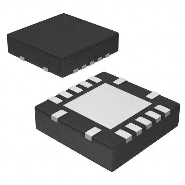
PACKAGE OUTLINE NGS0008C WSON - 0.8 mm max height SCALE 5.000 PLASTIC SMALL OUTLINE - NO LEAD 3.1 A B 2.9 PIN 1 INDEX AREA 2.6 2.4 0.8 C 0.7 SEATING PLANE 0.08 C 1.6 0.1 (0.1) TYP SYMM 0.05 EXPOSED 0.00 THERMAL PAD 4 5 9 SYMM 2X 1.5 0.1 1.5 1 8 6X 0.5 0.3 8X 0.2 PIN 1 ID 8X 0.5 0.1 C A B 0.3 0.05 C 4214924/A 07/2018 NOTES: 1. All linear dimensions are in millimeters. Any dimensions in parenthesis are for reference only. Dimensioning and tolerancing per ASME Y14.5M. 2. This drawing is subject to change without notice. 3. The package thermal pad must be soldered to the printed circuit board for thermal and mechanical performance. www.ti.com
EXAMPLE BOARD LAYOUT NGS0008C WSON - 0.8 mm max height PLASTIC SMALL OUTLINE - NO LEAD (1.6) 8X (0.6) SYMM 8 1 8X (0.25) (0.5) 9 SYMM (1.5) 6X (0.5) 4 5 ( 0.2) VIA TYP (R0.05) TYP (2.8) LAND PATTERN EXAMPLE EXPOSED METAL SHOWN SCALE:20X 0.07 MAX 0.07 MIN ALL AROUND ALL AROUND EXPOSED METAL EXPOSED METAL SOLDER MASK METAL METAL UNDER SOLDER MASK OPENING SOLDER MASK OPENING NON SOLDER MASK SOLDER MASK DEFINED DEFINED (PREFERRED) SOLDER MASK DETAILS 4214924/A 07/2018 NOTES: (continued) 4. This package is designed to be soldered to a thermal pad on the board. For more information, see Texas Instruments literature number SLUA271 (www.ti.com/lit/slua271). 5. Vias are optional depending on application, refer to device data sheet. If any vias are implemented, refer to their locations shown on this view. It is recommended that vias under paste be filled, plugged or tented. www.ti.com
EXAMPLE STENCIL DESIGN NGS0008C WSON - 0.8 mm max height PLASTIC SMALL OUTLINE - NO LEAD METAL 8X (0.6) SYMM TYP 1 8 8X (0.25) 9 SYMM (1.38) 6X (0.5) 4 5 (R0.05) TYP (1.47) (2.8) SOLDER PASTE EXAMPLE BASED ON 0.1 mm THICK STENCIL EXPOSED PAD 9: 82% PRINTED SOLDER COVERAGE BY AREA UNDER PACKAGE SCALE:20X 4214924/A 07/2018 NOTES: (continued) 6. Laser cutting apertures with trapezoidal walls and rounded corners may offer better paste release. IPC-7525 may have alternate design recommendations. www.ti.com
IMPORTANTNOTICEANDDISCLAIMER TI PROVIDES TECHNICAL AND RELIABILITY DATA (INCLUDING DATASHEETS), DESIGN RESOURCES (INCLUDING REFERENCE DESIGNS), APPLICATION OR OTHER DESIGN ADVICE, WEB TOOLS, SAFETY INFORMATION, AND OTHER RESOURCES “AS IS” AND WITH ALL FAULTS, AND DISCLAIMS ALL WARRANTIES, EXPRESS AND IMPLIED, INCLUDING WITHOUT LIMITATION ANY IMPLIED WARRANTIES OF MERCHANTABILITY, FITNESS FOR A PARTICULAR PURPOSE OR NON-INFRINGEMENT OF THIRD PARTY INTELLECTUAL PROPERTY RIGHTS. These resources are intended for skilled developers designing with TI products. You are solely responsible for (1) selecting the appropriate TI products for your application, (2) designing, validating and testing your application, and (3) ensuring your application meets applicable standards, and any other safety, security, or other requirements. These resources are subject to change without notice. TI grants you permission to use these resources only for development of an application that uses the TI products described in the resource. Other reproduction and display of these resources is prohibited. No license is granted to any other TI intellectual property right or to any third party intellectual property right. TI disclaims responsibility for, and you will fully indemnify TI and its representatives against, any claims, damages, costs, losses, and liabilities arising out of your use of these resources. TI’s products are provided subject to TI’s Terms of Sale (www.ti.com/legal/termsofsale.html) or other applicable terms available either on ti.com or provided in conjunction with such TI products. TI’s provision of these resources does not expand or otherwise alter TI’s applicable warranties or warranty disclaimers for TI products. Mailing Address: Texas Instruments, Post Office Box 655303, Dallas, Texas 75265 Copyright © 2020, Texas Instruments Incorporated