ICGOO在线商城 > 集成电路(IC) > 线性 - 音頻放大器 > NCP2811ADTBR2G

 Datasheet下载
- 型号: NCP2811ADTBR2G
- 制造商: ON Semiconductor
- 库位|库存: xxxx|xxxx
- 要求:
| 数量阶梯 | 香港交货 | 国内含税 |
| +xxxx | $xxxx | ¥xxxx |
查看当月历史价格
查看今年历史价格
NCP2811ADTBR2G产品简介:
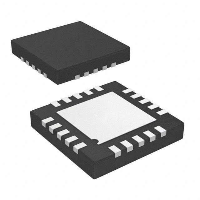
ICGOO电子元器件商城为您提供NCP2811ADTBR2G由ON Semiconductor设计生产,在icgoo商城现货销售,并且可以通过原厂、代理商等渠道进行代购。 NCP2811ADTBR2G价格参考。ON SemiconductorNCP2811ADTBR2G封装/规格:线性 - 音頻放大器, Amplifier IC Headphones, 2-Channel (Stereo) Class AB 14-TSSOP。您可以下载NCP2811ADTBR2G参考资料、Datasheet数据手册功能说明书,资料中有NCP2811ADTBR2G 详细功能的应用电路图电压和使用方法及教程。
NCP2811ADTBR2G是ON Semiconductor(安森美半导体)生产的一款线性音频放大器。这款器件主要应用于低功耗、高性能的音频信号放大场景,尤其适合便携式和电池供电设备。

应用场景:

1. 便携式音频设备:如MP3播放器、智能手机、平板电脑等。NCP2811ADTBR2G具有低功耗特性,能够在保证音质的同时延长电池续航时间,非常适合这些对功耗敏感的设备。

2. 耳机放大器:该芯片可以用于耳机放大电路中,提供高质量的音频输出,确保用户能够享受到清晰、纯净的声音体验。其高信噪比和低失真特性使得它在耳机驱动方面表现出色。

3. 语音助手和智能音箱:在智能家居产品中,NCP2811ADTBR2G可用于内置扬声器的音频放大,支持清晰的语音播报和音乐播放功能。它的低噪声和高效率有助于提升用户体验。

4. 汽车音响系统:尽管主要用于便携式设备,但NCP2811ADTBR2G也可应用于汽车音响系统中的辅助音频放大模块,提供稳定的音频输出,特别是在需要低功耗设计的情况下。

5. 医疗设备:如助听器或其他便携式医疗监测设备,这些设备通常要求小巧且高效的音频解决方案,以确保患者能够获得清晰的音频反馈,同时保持长时间的工作。

6. 物联网(IoT)设备:例如智能门铃、安防摄像头等带有音频功能的产品,NCP2811ADTBR2G可以为这些设备提供可靠的音频放大支持,确保语音通信的质量。

总之,NCP2811ADTBR2G凭借其低功耗、高性能的特点,在多种便携式和电池供电的音频应用中展现出广泛的应用前景。
| 参数 | 数值 |
| 产品目录 | 集成电路 (IC)半导体 |
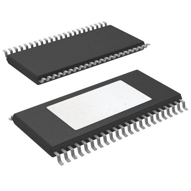
| 描述 | IC AMP STEREO HEADPHONE 14TSSOP音频放大器 HEADSET AUDIO AMP |
| 产品分类 | |
| 品牌 | ON Semiconductor |
| 产品手册 | |
| 产品图片 |
|
| rohs | 符合RoHS无铅 / 符合限制有害物质指令(RoHS)规范要求 |
| 产品系列 | 音频 IC,音频放大器,ON Semiconductor NCP2811ADTBR2GNOCAP™ |
| 数据手册 | |
| 产品型号 | NCP2811ADTBR2G |
| THD+噪声 | 1 % |
| 不同负载时的最大输出功率x通道数 | 110mW x 2 @ 16 欧姆 |
| 产品 | General Purpose Audio Amplifiers |
| 产品种类 | 音频放大器 |
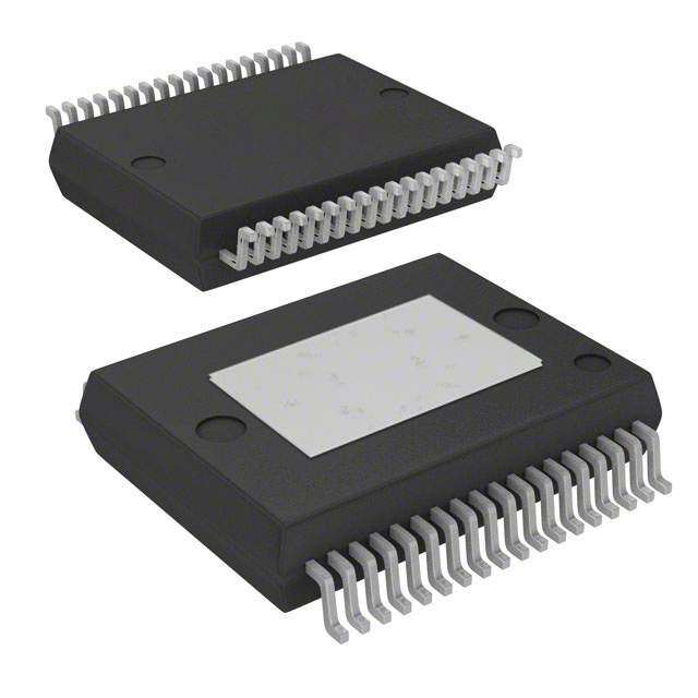
| 供应商器件封装 | 14-TSSOP |
| 其它名称 | NCP2811ADTBR2GOSCT |
| 包装 | 剪切带 (CT) |
| 商标 | ON Semiconductor |
| 增益 | - 1.5 V/V |
| 安装类型 | 表面贴装 |
| 安装风格 | SMD/SMT |
| 封装 | Reel |
| 封装/外壳 | 14-TSSOP(0.173",4.40mm 宽) |
| 封装/箱体 | TSSOP-14 |
| 工作温度 | -40°C ~ 85°C (TA) |
| 工作电源电压 | 2.7 V to 5 V |
| 工厂包装数量 | 2500 |
| 最大工作温度 | + 85 C |
| 最小工作温度 | - 40 C |
| 标准包装 | 1 |
| 特性 | 消除爆音,短路保护和热保护,关闭 |
| 电压-电源 | 2.7 V ~ 5 V |
| 电源电压-最大 | + 6 V |
| 电源电压-最小 | - 0.3 V |
| 电源电流 | 6 mA |
| 类型 | 2-Channel Stereo |
| 系列 | NCP2811 |
| 输出功率 | 27 mW |
| 输出类型 | 耳机,2-通道(立体声) |


- 商务部:美国ITC正式对集成电路等产品启动337调查
- 曝三星4nm工艺存在良率问题 高通将骁龙8 Gen1或转产台积电
- 太阳诱电将投资9.5亿元在常州建新厂生产MLCC 预计2023年完工
- 英特尔发布欧洲新工厂建设计划 深化IDM 2.0 战略
- 台积电先进制程称霸业界 有大客户加持明年业绩稳了
- 达到5530亿美元!SIA预计今年全球半导体销售额将创下新高
- 英特尔拟将自动驾驶子公司Mobileye上市 估值或超500亿美元
- 三星加码芯片和SET,合并消费电子和移动部门,撤换高东真等 CEO
- 三星电子宣布重大人事变动 还合并消费电子和移动部门
- 海关总署:前11个月进口集成电路产品价值2.52万亿元 增长14.8%


PDF Datasheet 数据手册内容提取
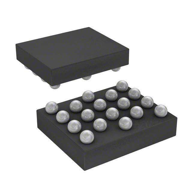
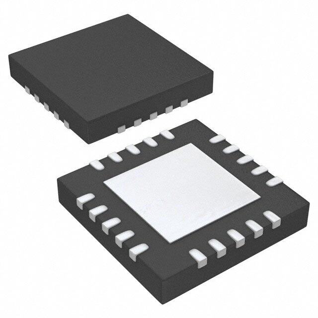
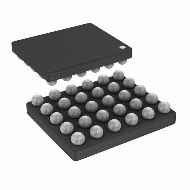
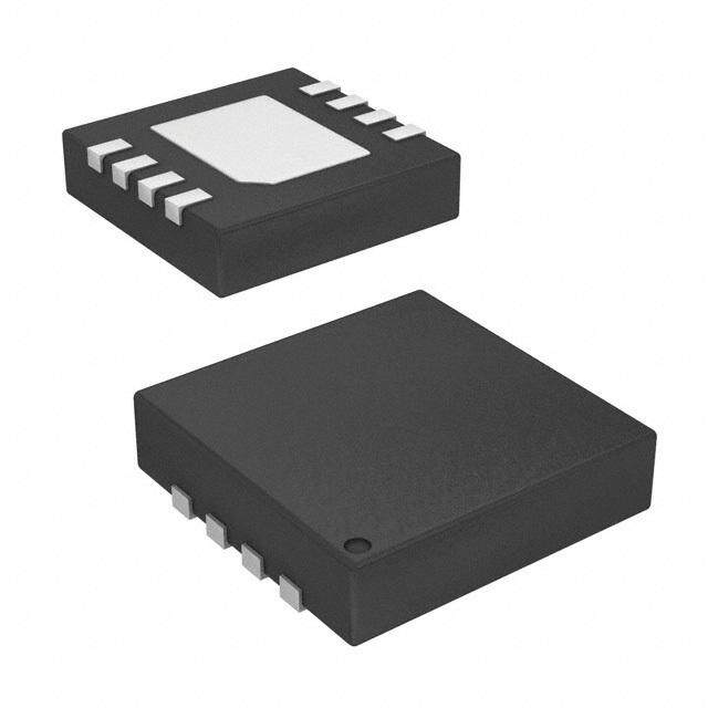
NCP2811 NOCAP(cid:2) Advanced Stereo Headphone Amplifier NCP2811 is a dual audio power amplifier designed for portable communication device applications such as mobile phones. This part is capable of delivering 27 mW of continuous average power into a 16Ω load from a 2.7 V power supply with a THD+N of 1%. http://onsemi.com Based on the power supply delivered to the device, an internal MARKING power management block generates a symmetrical positive and DIAGRAMS negative voltage. Thus, the internal amplifiers provide outputs referenced to Ground. In this True Ground configuration, the two 12 PIN CSP 2811xz external heavy coupling capacitors can be removed. It offers FC SUFFIX AYWW significant space and cost savings compared to a typical stereo CASE 499AZ (cid:2) application. x = A for NCP2811A NCP2811 is available with an external adjustable gain (version A), = B for NCP2811B or with an internal gain of −1.5 V/V (version B). It reaches a superior z = C for backside laminate −100dB PSRR and noise floor. Thus, it offers high fidelity audio A = Assembly Location sound, as well as a direct connection to the battery. It contains circuitry Y = Year to prevent from “Pop & Click” noise that would otherwise occur WW= Work Week (cid:2) = Pb−Free Package during turn−on and turn−off transitions. The device is available in 12 bump CSP package (2 x 1.5 mm) which help to save space on the board. It is also available in WQFN12 and TSSOP−14 packages. WQFN12 2811x MT SUFFIX ALYW(cid:2) Features 1 CASE 510AH (cid:2) • True Ground Configuration Output Eliminates DC−Blocking Capacitors: x = A for NCP2811A − Save Board Area = B for NCP2811B A = Assembly Location − Save Component Cost L = Wafer Lot − No Low−Frequency Response Attenuation Y = Year • High PSRR (−100 dB): Direct Connection to the Battery W = Work Week • (cid:2) = Pb−Free Package “Pop and Click” Noise Protection Circuitry • (Note: Microdot may be in either location) Internal Gain (−1.5 V/V) or External Adjustable Gain • Ultra Low Current Shutdown Mode • 14 2.7 V – 5.0 V Operation 2811 • Thermal Overload Protection Circuitry 14 TSSOP−14 x • CSP 2 x 1.5 mm 1 DTB SUFFIX ALYW(cid:2) CASE 948G (cid:2) • WQFN12 3 x 3 mm 1 • TSSOP−14 • x = A for NCP2811A These Devices are Pb−Free, Halogen Free/BFR Free and are RoHS = B for NCP2811B Compliant A = Assembly Location L = Wafer Lot Typical Applications Y = Year • W = Work Week Headset Audio Amplifier for (cid:2) = Pb−Free Package − Cellular Phones (Note: Microdot may be in either location) − MP3 Player − Personal Digital Assistant and Portable Media Player − Portable Devices ORDERING INFORMATION See detailed ordering and shipping information on page 12 of this data sheet. © Semiconductor Components Industries, LLC, 2010 1 Publication Order Number: November, 2010 − Rev. 3 NCP2811/D
NCP2811 1 (cid:2)F 1 (cid:2)F 1 (cid:2)F 1 (cid:2)F P M P M VP P P VP P P C C C C B1 C1 C3 1 (cid:2)F B1 C1 C3 1 (cid:2)F Audio Left B3 VP CPPCPMPGPVNMD C2 C4 PVM Audio Left B3 VP CPPCPMPGPVNMD C2 C4 PVM INL SPVM INL SPVM SD A2 B4 SD A2 B4 SD A4 10 OUTL SD A4 10 OUTL Audio Right B2 OUTL Audio Right B2 OUTL INR A3 OUTR INR A3 OUTR OUTR OUTR AGND 10 AGND 10 A1 A version A1 B version Figure 1. Application Schematics WQFN12 L R 12 PIN CSP T T TSSOP14 P U U V O O NC OUTL A1 A2 A3 A4 VP OUTR CPP NC AGND SD OUTR OUTL CPP NC PGND INR B1 B2 B3 B4 PGND INR CPM AGND CPM AGND VP INR INL SPVM PVM INL C1 C2 C3 C4 SD NC CPP PGND CPM PVM VM SD NL P I (Top View) (Top View) (Top View) Figure 2. Pin Configurations http://onsemi.com 2
NCP2811 VP 1 (cid:2)F Cs 1 (cid:2)F VP CPP CPM VRP PGND PVM 1 (cid:2)F POWER MANAGEMENT SPVM VRM Left Audio VRP INL − OUTL + VRM Use 10 ohm SD BIASING CLICK/POP resistor for SUPPRESSION capacitive drive VRP capability + Right OUTR Audio INR − VRM AGND Figure 3. Typical Application Schematic version A http://onsemi.com 3
NCP2811 VP 1 (cid:2)F Cs 1 (cid:2)F CPP CPM VP VRP PGND PVM 1 (cid:2)F POWER MANAGEMENT VRM Left Audio VRP INL − OUTL + VRM Use 10 ohm resistor SD BIASING CLICK/POP for capacitive SUPPRESSION drive capability VRP + Right OUTR Audio INR − VRM AGND Figure 4. Typical Application Schematic version B Table 1. PIN FUNCTION DESCRIPTION PIN PIN PIN TS- PIN CSP TQFN SOP NAME TYPE DESCRIPTION A1 7 10 AGND GROUND Analog ground. Connect to ground reference A2 5 7 SD INPUT Enable activation A3 10 13 OUTR OUTPUT Right audio channel output signal A4 11 14 OUTL OUTPUT Left audio channel output signal B1 12 2 VP POWER Positive supply voltage. It can be connected for example to a Lithium/Ion battery B2 8 11 INR INPUT Right input of the first audio source B3 6 9 INL INPUT Left input of the first audio source B4 − − SPVM POWER Amplifier negative power supply voltage. Connect to PVM C1 1 3 CPP INPUT/ Charge pump flying capacitor positive terminal. A 1 (cid:2)F ceramic filtering OUTPUT capacitor to CPM is needed C2 2 4 PGND GROUND Power ground, connect to ground reference C3 3 5 CPM INPUT Charge pump flying capacitor negative terminal. A 1 (cid:2)F ceramic filtering capacitor to CPP is needed C4 4 6 PVM OUTPUT Charge pump output. A 1 (cid:2)F ceramic filtering capacitor to ground is needed http://onsemi.com 4
NCP2811 Table 2. MAXIMUM RATINGS Rating Symbol Value Unit AVIN, PVIN Pins: Power Supply Voltage (Note 2) VP − 0.3 to + 6.0 V INL, INR Pins: Input (Note 2) VIN V A version −VP – 0.3 to VP + 0.3 B version −2 to +2 SD Pin: Input (Note 2) VYY −0.3 to VP + 0.3 V Human Body Model (HBM) ESD Rating are (Note 3) ESD HBM 2000 V Machine Model (MM) ESD Rating are (Note 3) ESD MM 200 V CSP 1.5 x 2.0 mm package (Notes 6 and 7) R(cid:3)JC (Note 7) °C/W Thermal Resistance Junction to Case Operating Ambient Temperature Range TA −40 to + 85 °C Operating Junction Temperature Range TJ −40 to + 125 °C Maximum Junction Temperature (Note 6) TJMAX + 150 °C Storage Temperature Range TSTG −65 to + 150 °C Moisture Sensitivity (Note 5) MSL Level 1 Stresses exceeding Maximum Ratings may damage the device. Maximum Ratings are stress ratings only. Functional operation above the Recommended Operating Conditions is not implied. Extended exposure to stresses above the Recommended Operating Conditions may affect device reliability. Notes: 1. Maximum electrical ratings are defined as those values beyond which damage to the device may occur at TA = 25°C. 2. According to JEDEC standard JESD22−A108B. 3. This device series contains ESD protection and passes the following tests: Human Body Model (HBM) ±2.0 kV per JEDEC standard: JESD22−A114 for all pins. Machine Model (MM) ±200 V per JEDEC standard: JESD22−A115 for all pins. 4. Latch up Current Maximum Rating: ±100 mA per JEDEC standard: JESD78 class II. 5. Moisture Sensitivity Level (MSL): 1 per IPC/JEDEC standard: J−STD−020A. 6. The thermal shutdown set to 150°C (typical) avoids irreversible damage on the device due to power dissipation. 7. The RJA is highly dependent of the PCB Heatsink area. For example, RJA can equal 195°C/W with 50 mm2 total area and also 135°C/W with 50mm2. The bumps have the same thermal resistance and all need to be connected to optimize the power dissipation. 125(cid:3)T R(cid:3)CA(cid:2) P A(cid:3)R(cid:3)JC D http://onsemi.com 5
NCP2811 Table 3. ELECTRICAL CHARACTERISTICS Min & Max Limits apply for TA between −40°C to +85°C and TJ up to + 125°C for VIN between 2.7 V to 5.0 V (Unless otherwise noted). Typical values are referenced to TA = + 25°C and VIN = 3.6 V. Symbol Parameter Conditions Min Typ Max Unit VP Operational Power Supply 2.7 5.0 V IDD Supply quiescent current Both channels enabled 6.0 mA ISD Shutdown current VP = 2.7 V to 5.0 V 1 (cid:2)A VOS Output offset voltage VP = 2.7 V to 5.0 V ±1 mV VIH High−Level input voltage SD pin 1.2 V VIL Low−Level input voltage SD pin 0.4 V RSD SD pin pull−down impedance 190 K(cid:4) TWU Turning on time 1 ms TSD Thermal shutdown temperature 160 °C VLP Max output swing (peak value) VP = 2.9 V to 5.0 V 1 VRMS Headset ≥ 16 (cid:4) THD+N = 1% PO Max output power (output in phase) VP = 2.7V, THD+N = 1% 27 mW Headset = 16 (cid:4) VP = 2.7V, THD+N = 1% 37 Headset = 32 (cid:4) VP = 3.6V, THD+N = 1% 90 Headset = 16 (cid:4) VP = 3.6V, THD+N = 1% 64 Headset = 32 (cid:4) VP = 5.0V, THD+N = 1% 110 Headset = 16 (cid:4) VP = 5.0V, THD+N = 1% 64 Headset = 32 (cid:4) Crosstalk (Note 8) Headset ≥ 16 (cid:4) −80 −60 dB PSRR Power supply rejection ratio (Note 8) VP = 2.7 V to 5.0 V dB Input shorted to ground F = 217 Hz −106 F = 1 kHz −95 THD+N Total harmonic distortion + noise (Note 8) Headset = 16 (cid:4) 0.01 % POUT = 25 mW VN Output noise voltage (Note 8) A−Weighting filter 7 (cid:2)VRMS ZIN Input impedance B version only 20 K(cid:4) ZSD Output impedance in shutdown mode 10 K(cid:4) UVLO UVLO threshold Falling edge 2.3 V UVLOHYST UVLO hysteresis 100 mV Av Voltage Gain B version only −1.53 −1.5 −1.48 V/V 8. Guaranteed by design and characterized. http://onsemi.com 6
NCP2811 TYPICAL OPERATING CHARACTERISTICS 100 100 16 (cid:4) in Phase 16 (cid:4) out of Phase 10 10 %) 1 %) 1 N ( N ( + + D D H 0.1 H 0.1 THD+N_L (%) T THD+N_L (%) T THD+N_R (%) 0.01 0.01 THD+N_R (%) 0.001 0.001 0 20 40 60 80 100 120 140 160 0 20 40 60 80 100 120 140 160 180 Pout (mW) Pout (mW) Figure 5. THD+N vs. Pout @ Vp = 3.6 V Figure 6. THD+N vs. Pout @ Vp = 3.6 V 100 100 16 (cid:4) in Phase 16 (cid:4) out of Phase 2.7 V 2.7 V 10 10 3.0 V 3.0 V 3.6 V %) 1 3.6 V %) 1 D ( D ( H H 4.2 V T 0.1 T 0.1 4.2 V Vp = 5 V Vp = 5 V 0.01 0.01 0.001 0.001 0 20 40 60 80 100 120 140 160 180 0 20 40 60 80 100 120 140 160 180 Pout (mW) Pout (mW) Figure 7. THD+N vs. Pout LEFT Figure 8. THD+N vs. Pout RIGHT 100 100 16 (cid:4) out of Phase 16 (cid:4) out of Phase 2.7 V 2.7 V 10 3.0 V 10 3.0 V 3.6 V %) 1 4.32. 6V V %) 1 4.2 V D ( Vp = 5 V D ( Vp = 5 V H H T 0.1 T 0.1 0.01 0.01 0.001 0.001 0 20 40 60 80 100 120 140 160 180 0 20 40 60 80 100 120 140 160 180 Pout (mW) Pout (mW) Figure 9. THD+N vs. Pout LEFT Figure 10. THD+N vs. Pout RIGHT http://onsemi.com 7
NCP2811 TYPICAL OPERATING CHARACTERISTICS 100 100 32 (cid:4) in Phase 32 (cid:4) out of Phase 10 10 THD+N_L (%) THD+N_L (%) %) 1 %) 1 N ( THD+N_R (%) N ( + + THD+N_R (%) D D H 0.1 H 0.1 T T 0.01 0.01 0.001 0.001 0 10 20 30 40 50 60 70 80 90 100 0 10 20 30 40 50 60 70 80 90 100 Pout (mW) Pout (mW) Figure 11. THD+N vs. Pout @ Vp = 3.6 V Figure 12. THD+N vs. Pout @ Vp = 3.6 V 100 100 32 (cid:4) in Phase 32 (cid:4) in Phase 2.7 V 2.7 V 10 3.0 V 10 3.0 V 3.6 V 3.6 V %) 1 4.2 V %) 1 4.2 V D ( Vp = 5 V D ( Vp = 5 V H H T 0.1 T 0.1 0.01 0.01 0.001 0.001 0 10 20 30 40 50 60 70 80 90 100 0 10 20 30 40 50 60 70 80 90 100 Pout (mW) Pout (mW) Figure 13. THD+N vs. Pout LEFT Figure 14. THD+N vs. Pout RIGHT 100 100 32 (cid:4) out of Phase 32 (cid:4) out of Phase 10 10 2.7 V 2.7 V 3.0 V 3.0 V %) 1 3.6 V %) 1 3.6 V D ( 4.2 V D ( 4.2 V H H T 0.1 T 0.1 Vp = 5 V Vp = 5 V 0.01 0.01 0.001 0.001 0 10 20 30 40 50 60 70 80 90 100 0 10 20 30 40 50 60 70 80 90 100 Pout (mW) Pout (mW) Figure 15. THD+N vs. Pout LEFT Figure 16. THD+N vs. Pout RIGHT http://onsemi.com 8
NCP2811 TYPICAL OPERATING CHARACTERISTICS 1 1 16 (cid:4) out of Phase 16 (cid:4) out of Phase 0.1 0.1 %) VP = 3.6 V %) N ( VP = 5.0 V N ( + + D D VP = 3.6 V H H T T 0.01 0.01 VP = 2.7 V VP = 2.7 V VP = 5.0 V 0.001 0.001 10 100 1,000 10,000 100,000 10 100 1,000 10,000 100,000 FREQUENCY (Hz) FREQUENCY (Hz) Figure 17. THD vs. Frequency LEFT Figure 18. THD vs. Frequency RIGHT @ Pout = 32 mW @ Pout = 32 mW 1 1 32 (cid:4) out of Phase 32 (cid:4) out of Phase VP = 2.7 V VP = 2.7 V VP = 3.6 V VP = 3.6 V 0.1 0.1 %) VP = 5.0 V %) VP = 5.0 V N ( N ( + + D D H H T T 0.01 0.01 0.001 0.001 10 100 1,000 10,000 100,000 10 100 1,000 10,000 100,000 FREQUENCY (Hz) FREQUENCY (Hz) Figure 19. THD vs. Frequency LEFT Figure 20. THD vs. Frequency RIGHT @ Pout = 32 mW @ Pout = 32 mW 140 80 85°C 120 25°C 70 25°C 60 100 85°C 50 W) 80 −40°C W) 40 −40°C m m ( 60 ( 30 40 20 20 10 0 0 2.7 3.2 3.7 4.2 4.7 2.7 3.2 3.7 4.2 4.7 VP (V) VP (V) Figure 21. Maximum Output Power LEFT vs. Figure 22. Maximum Output Power LEFT vs. VP (THD+N < 1%) VP (THD+N < 0.1%) http://onsemi.com 9
NCP2811 TYPICAL OPERATING CHARACTERISTICS 0 −60 −65 −20 −70 −75 −40 −80 B) −85 Left to Right d RR ( −60 (dB) −90 S −95 Right to Left P −80 −100 NCP2811B Left −105 −100 −110 −115 NCP2811B Right −120 −120 10 100 1000 10,000 100,000 10 100 1000 10,000 100,000 FREQUENCY (Hz) FREQUENCY (Hz) Figure 23. PSRR at Vp = 3.6 V Figure 24. Crosstalk vs. Frequency @ Vp = 3.6 V http://onsemi.com 10
NCP2811 DETAIL OPERATING DESCRIPTION Detailed Descriptions filter with R (externally selectable for A version, 20 k(cid:4) for in The NCP2811 is a stereo headphone amplifier with a true B version). ground architecture. This architecture eliminates the need to The size of the capacitor must be large enough to couple use 2 external big capacitors required by conventional in low frequencies without severe attenuation in the audio headphone amplifier. bandwith (20 Hz – 20 kHz). The structure of the NCP2811 is basically composed of 2 The cut off frequency for the input high−pass filter is: true ground amplifiers, an UVLO, a short circuit protection and also a thermal shutdown. A special circuitry is Fc(cid:2)2(cid:5)R1C in in embedded to eliminate any pop and click noise that occurs A F < 20 Hz is recommended. c during turn on and turn off time. The A version has an external gain selectable by two resistor, B version has a gain Charge Pump Capacitor Selection of 1.5 V/V. Use ceramic capacitor with low ESR for better performances. X5R / X7R capacitor is recommended. NOCAP(cid:2) The flying capacitor (C2) serves to transfer charge during NOCAP(cid:3) is a patented architecture which requires only the generation of the negative voltage. 2 small ceramic capacitors. It generates a symmetrical The CPVM capacitor (C3) must be equal at least to the positive and negative voltage and it allows the output of the CFly capacitor to allow maximum transfer charge. The amplifiers to be biased around the ground. CPVM value must not exceed 1 (cid:2)F. Higher capacitor value can damage the part. Current Limit Protection Circuit The NCP2811 embed a protection circuitry against short Table 4 suggests typical value and manufacturer: to ground. When an output is shorted to GND and when a Table 4. signal appears at the input, the current is limited to 300 mA. Value Reference Package Manufacturer Thermal Overload Protection 1 (cid:2)F C1005X5R0J105K 0402 TDK Internal amplifiers are switched off when the temperature exceed 160°C, and will be switch on again when the 1 (cid:2)F GRM155R60J105K19 0402 Murata temperature decrease below 140°C. Lower value of capacitors can be used but the maximum output power is reduced and the device may not operate to Under Voltage Lockout specifications. When the battery voltage decreases below 2.3 V, the amplifiers are turned off. The hysteresis to turn on it again Power Supply Decoupling Capacitor (C1) is 100mV. The NCP2811 is a True Ground amplifier which requires the adequate decoupling capacitor to reduce noise and Pop and Click Suppression Circuitry THD+N. Use X5R / X7R ceramic capacitor and place it The NCP2811 includes a special circuitry to eliminate any closed to the CPVDD pin. A value of 1 (cid:2)F is recommended. pop and click noise during turn on and turn off time. Basic amplifier creates an offset during these transitions at the Shutdown Function output which give a parasitic noise called “pop and click The device enters in shutdown mode when shutdown signal noise”. The NCP2811 eliminates this problem. is low. During the shutdown mode, the DC quiescent current of the circuit does not exceed 500 nA. In this configuration, Gain Setting Resistor Selection (Rin & Rf, A version the output impedance is 10 k(cid:4) on each output. only) R and R set the closed loop gain of the amplifier. A low in f Output Resistor for Capacitive Drive Capability gain configuration (close to 1) minimizes the THD + noise Under normal operation, NCP2811 maximum direct values and maximizes the signal to noise ratio. capacitive load is in the 80 pF range. If, for any reason, high A closed loop gain in the range of 1 to 10 is recommended value capacitive loads should be connected to NCP2811 to optimize overall system performance. outputs, an additional 10 (cid:4) resistor should be placed The formula to calculate the gain is: between the NCP2811 output and the capacitive load to R ensure amplifier stability. Av(cid:2)(cid:3) f R in Layout Recommendation Connect C1 as close as possible of the Vp pin. Input Capacitor Selection Connect C2 and C3 as close as possible of the NCP2811. The input coupling capacitor blocks the DC voltage at the Route audio signal and AGND far from Vp, CPP, CPM, amplifier input terminal. This capacitor creates a high−pass PVM and PGND to avoid any perturbation due to the switching. http://onsemi.com 11
NCP2811 Table 5. ORDERING INFORMATION Device Package Shipping† NCP2811ADTBR2G TSSOP−14 2500/Tape & Reel (Pb−Free) NCP2811BDTBR2G TSSOP−14 2500/Tape & Reel (Pb−Free) NCP2811AFCT1G Flip−Chip 12 3000/Tape & Reel (Pb−Free) NCP2811BFCT1G Flip−Chip 12 3000/Tape & Reel (Pb−Free) NCP2811BFCCT1G Flip−Chip 12 3000/Tape & Reel (Backside Laminate Coating) (Pb−Free) NCP2811AMTTXG WQFN12 3000/Tape & Reel (Pb−Fre) NCP2811BMTTXG WQFN12 3000/Tape & Reel (Pb−Free) †For information on tape and reel specifications, including part orientation and tape sizes, please refer to our Tape and Reel Packaging Specifications Brochure, BRD8011/D. PACKAGE DIMENSIONS 12 PIN FLIP−CHIP, 2.0x1.5, 0.5P CASE 499AZ−01 ISSUE O NOTES: D A B 1. DIMENSIONING AND TOLERANCING PER ASME Y14.5M, 1994. PIN A1 REFERENCE 2. CONTROLLING DIMENSION: MILLIMETERS. 3. COPLANARITY APPLIES TO SPHERICAL CROWNS OF SOLDER BALLS. 2X E MILLIMETERS 0.10 C DIM MIN MAX A 0.54 0.60 2X 0.10 C A1 0.21 0.27 TOP VIEW A2 0.33 0.39 b 0.29 0.34 D 2.00 BSC A A2 E 1.50 BSC 0.10 C A1 e 0.50 BSC 12X 0.05 C C SEATING SOLDERING FOOTPRINT* NOTE 3 SIDE VIEW PLANE 0.5 PITCH 0.5 A1 PITCH e/2 e 12X b e 0.05 C A B C 0.03 C B 12X 0.25 PACKAGE OUTLINE A 1 2 3 4 BOTTOM VIEW http://onsemi.com 12
NCP2811 PACKAGE DIMENSIONS WQFN12 3x3, 0.5P CASE 510AH−01 ISSUE O NOTES: L L 1. DIMENSIONING AND TOLERANCING PER D A B ASME Y14.5M, 1994. 2. CONTROLLING DIMENSION: MILLIMETERS. 3. DIMENSION b APPLIES TO PLATED PIN ONE ÇÇÇ L1 TERMINAL AND IS MEASURED BETWEEN REFERENCE 0.15 AND 0.30 MM FROM TERMINAL TIP. ÇÇÇ 4. COPLANARITY APPLIES TO THE EXPOSED DETAIL A PAD AS WELL AS THE TERMINALS. ÇÇÇ E COANLSTTERRUNCATTIOENS MILLIMETERS DIM MIN MAX A 0.65 0.85 2X 0.10 C EXPOSED ÇCu ÇMÇOLD CMPD ÉÉA3 AA13 0.00.022 RE0F.05 b 0.20 0.30 ÇÉÇÉÇÉ ÉÇÉÇ D 3.00 BSC 2X 0.10 C D2 1.30 1.50 TOP VIEW E 3.00 BSC DETAIL B A A1 Ee2 1.03.050 BS1C.50 0.10 C A3 DETAIL B K 0.20 −−− ALTERNATE L 0.30 0.50 CONSTRUCTIONS L1 0.00 0.15 13X 0.10 C NOTE 4 SIDE VIEW A1 C SPELAATNIENG SOLDERING FOOTPRINT* 12X 0.63 D2 PACKAGE DETAIL A OUTLINE 4 12X L 1 7 2X 2X E2 12Xb 1.50 3.30 0.10 C A BB 1 0.05 C NOTE 3 12X 0.30 K 12 e 0.50 PITCH BOTTOM VIEW DIMENSIONS: MILLIMETERS *For additional information on our Pb−Free strategy and soldering details, please download the ON Semiconductor Soldering and Mounting Techniques Reference Manual, SOLDERRM/D. http://onsemi.com 13
NCP2811 PACKAGE DIMENSIONS TSSOP−14 CASE 948G−01 ISSUE B 14X K REF NOTES: 1. DIMENSIONING AND TOLERANCING PER 0.10 (0.004) M T U S V S ANSI Y14.5M, 1982. 2. CONTROLLING DIMENSION: MILLIMETER. 0.15 (0.006) T U S 3. DIMENSION A DOES NOT INCLUDE MOLD FLASH, PROTRUSIONS OR GATE BURRS. N MOLD FLASH OR GATE BURRS SHALL NOT 0.25 (0.010) EXCEED 0.15 (0.006) PER SIDE. 14 8 4. DIMENSION B DOES NOT INCLUDE 2XL/2 INTERLEAD FLASH OR PROTRUSION. M INTERLEAD FLASH OR PROTRUSION SHALL NOT EXCEED 0.25 (0.010) PER SIDE. L B 5. DIMENSION K DOES NOT INCLUDE DAMBAR −U− N PROTRUSION. ALLOWABLE DAMBAR PIN 1 PROTRUSION SHALL BE 0.08 (0.003) TOTAL IDENT. F IN EXCESS OF THE K DIMENSION AT MAXIMUM MATERIAL CONDITION. 1 7 DETAIL E 6. TERMINAL NUMBERS ARE SHOWN FOR REFERENCE ONLY. 7. DIMENSION A AND B ARE TO BE DETERMINED AT DATUM PLANE −W−. 0.15 (0.006) T U S A K MILLIMETERS INCHES −V− ÇÉÇÉK1ÇÉ DIM MIN MAX MIN MAX A 4.90 5.10 0.193 0.200 ÇÉÇÉÇÉ B 4.30 4.50 0.169 0.177 J J1 C −−− 1.20 −−− 0.047 D 0.05 0.15 0.002 0.006 ÇÇÇ F 0.50 0.75 0.020 0.030 SECTION N−N G 0.65 BSC 0.026 BSC H 0.50 0.60 0.020 0.024 J 0.09 0.20 0.004 0.008 −W− J1 0.09 0.16 0.004 0.006 C K 0.19 0.30 0.007 0.012 K1 0.19 0.25 0.007 0.010 0.10 (0.004) L 6.40 BSC 0.252 BSC M 0 (cid:4) 8 (cid:4) 0 (cid:4) 8 (cid:4) −T− SEATING D G H DETAIL E PLANE SOLDERING FOOTPRINT 7.06 1 0.65 PITCH 14X 14X 0.36 1.26 DIMENSIONS: MILLIMETERS ON Semiconductor and are registered trademarks of Semiconductor Components Industries, LLC (SCILLC). SCILLC reserves the right to make changes without further notice to any products herein. SCILLC makes no warranty, representation or guarantee regarding the suitability of its products for any particular purpose, nor does SCILLC assume any liability arising out of the application or use of any product or circuit, and specifically disclaims any and all liability, including without limitation special, consequential or incidental damages. “Typical” parameters which may be provided in SCILLC data sheets and/or specifications can and do vary in different applications and actual performance may vary over time. All operating parameters, including “Typicals” must be validated for each customer application by customer’s technical experts. SCILLC does not convey any license under its patent rights nor the rights of others. SCILLC products are not designed, intended, or authorized for use as components in systems intended for surgical implant into the body, or other applications intended to support or sustain life, or for any other application in which the failure of the SCILLC product could create a situation where personal injury or death may occur. Should Buyer purchase or use SCILLC products for any such unintended or unauthorized application, Buyer shall indemnify and hold SCILLC and its officers, employees, subsidiaries, affiliates, and distributors harmless against all claims, costs, damages, and expenses, and reasonable attorney fees arising out of, directly or indirectly, any claim of personal injury or death associated with such unintended or unauthorized use, even if such claim alleges that SCILLC was negligent regarding the design or manufacture of the part. SCILLC is an Equal Opportunity/Affirmative Action Employer. This literature is subject to all applicable copyright laws and is not for resale in any manner. PUBLICATION ORDERING INFORMATION LITERATURE FULFILLMENT: N. American Technical Support: 800−282−9855 Toll Free ON Semiconductor Website: www.onsemi.com Literature Distribution Center for ON Semiconductor USA/Canada P.O. Box 5163, Denver, Colorado 80217 USA Europe, Middle East and Africa Technical Support: Order Literature: http://www.onsemi.com/orderlit Phone: 303−675−2175 or 800−344−3860 Toll Free USA/Canada Phone: 421 33 790 2910 Fax: 303−675−2176 or 800−344−3867 Toll Free USA/Canada Japan Customer Focus Center For additional information, please contact your local Email: orderlit@onsemi.com Phone: 81−3−5773−3850 Sales Representative http://onsemi.com NCP2811/D 14
Mouser Electronics Authorized Distributor Click to View Pricing, Inventory, Delivery & Lifecycle Information: O N Semiconductor: NCP2811ADTBR2G NCP2811AFCT1G NCP2811BDTBR2G NCP2811BFCCT1G