ICGOO在线商城 > 集成电路(IC) > 线性 - 音頻放大器 > MAX98355BEWL+T

 Datasheet下载
- 型号: MAX98355BEWL+T
- 制造商: Maxim
- 库位|库存: xxxx|xxxx
- 要求:
| 数量阶梯 | 香港交货 | 国内含税 |
| +xxxx | $xxxx | ¥xxxx |
查看当月历史价格
查看今年历史价格
MAX98355BEWL+T产品简介:
ICGOO电子元器件商城为您提供MAX98355BEWL+T由Maxim设计生产,在icgoo商城现货销售,并且可以通过原厂、代理商等渠道进行代购。 MAX98355BEWL+T价格参考。MaximMAX98355BEWL+T封装/规格:线性 - 音頻放大器, Amplifier IC 1-Channel (Mono) Class D 9-WLP。您可以下载MAX98355BEWL+T参考资料、Datasheet数据手册功能说明书,资料中有MAX98355BEWL+T 详细功能的应用电路图电压和使用方法及教程。
MAX98355BEWL+T 是 Maxim Integrated 公司推出的一款高效、低功耗的单声道 D 类音频放大器,属于线性 - 音频放大器分类。其主要应用场景包括便携式设备、电池供电系统以及对音频性能和能效有较高要求的电子产品。以下是该型号的具体应用场景分析:

 1. 便携式消费电子设备
   - 智能手机和平板电脑:MAX98355BEWL+T 的低功耗特性和高效率使其非常适合用于智能手机和平板电脑中的扬声器驱动。它能够提供高质量的声音输出,同时减少电池消耗。
   - 蓝牙音箱和无线耳机:在小型化、电池供电的音频设备中,这款放大器可以实现清晰的音质输出,并延长设备的续航时间。

 2. 物联网 (IoT) 设备
   - 智能音箱和语音助手:MAX98355BEWL+T 支持高保真音频输出,适用于需要高品质声音的智能音箱或语音助手设备,例如亚马逊 Echo 或谷歌 Nest 等产品。
   - 智能家居设备:如门铃摄像头、智能灯泡等需要内置扬声器的产品,可利用该放大器提供清晰的提示音或语音信息。

 3. 可穿戴设备
   - 智能手表和健康追踪器:这些设备通常需要微型化的音频解决方案,而 MAX98355BEWL+T 的小尺寸封装(WLP 封装)和低功耗特性非常适配。
   - 助听器和听力辅助设备:由于其高效的音频处理能力,该放大器可用于提升小型听力设备的音质表现。

 4. 汽车电子
   - 车载信息娱乐系统:在汽车导航、多媒体播放等场景中,这款放大器可以为仪表盘或后视镜上的小型扬声器提供稳定的音频输出。
   - 电动车报警系统:电动车需要低噪音、高效率的音频模块来发出提示音或警报声,MAX98355BEWL+T 能满足这一需求。

 5. 工业与医疗设备
   - 医疗监护仪和诊断设备:如超声波设备、心电图机等可能需要音频反馈的场合,这款放大器可以提供稳定且低失真的声音输出。
   - 工业控制面板和人机界面 (HMI):在工厂自动化或实验室设备中,用于播放操作提示音或报警信号。

 核心优势
- 高效率:D 类放大技术确保了更高的能量转换效率,降低发热问题。
- 低失真:支持高质量音频输出,适合对音质敏感的应用。
- 小尺寸封装:便于集成到空间受限的设备中。
- 低功耗:延长电池寿命,特别适合移动设备。

综上所述,MAX98355BEWL+T 广泛应用于各类便携式、电池供电及对音频性能有较高要求的设备中,是一款兼具高效、低功耗和高音质的音频放大器解决方案。
| 参数 | 数值 |
| 产品目录 | 集成电路 (IC) |
| 描述 | IC AUDIO AMP PCM D 9WLP |
| 产品分类 | |
| 品牌 | Maxim Integrated |
| 数据手册 | |
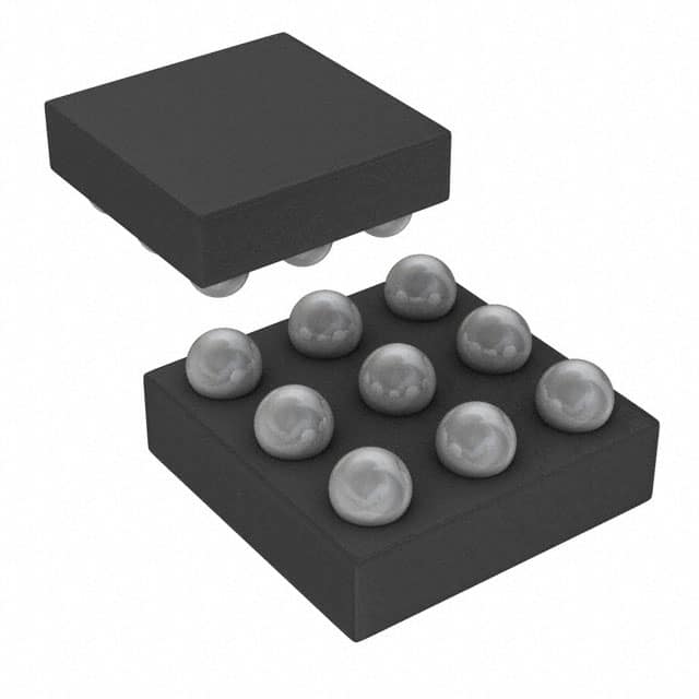
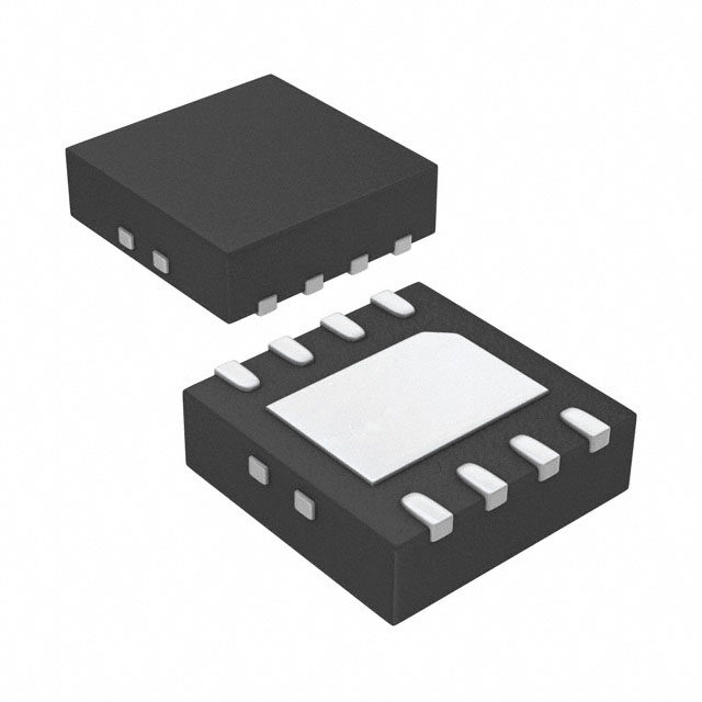
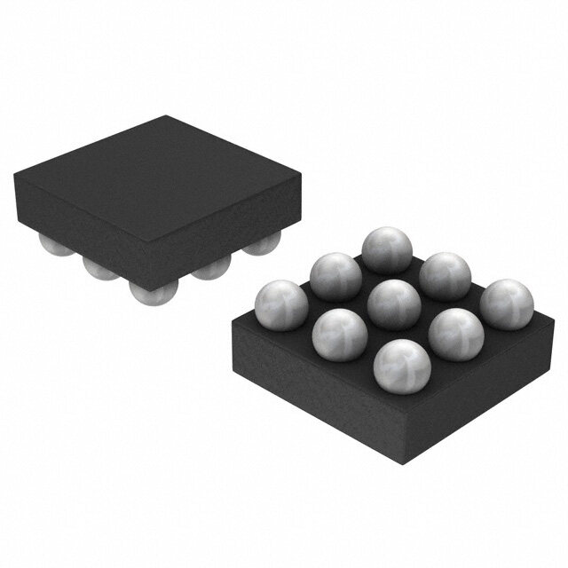
| 产品图片 |
|
| 产品型号 | MAX98355BEWL+T |
| rohs | 无铅 / 符合限制有害物质指令(RoHS)规范要求 |
| 产品系列 | - |
| 不同负载时的最大输出功率x通道数 | 3.2W x 1 @ 4 欧姆 |
| 供应商器件封装 | 9-WLP |
| 其它名称 | MAX98355BEWL+TDKR |
| 包装 | Digi-Reel® |
| 安装类型 | 表面贴装 |
| 封装/外壳 | 9-UFBGA |
| 工作温度 | -40°C ~ 85°C (TA) |
| 应用说明 | |
| 标准包装 | 1 |
| 特性 | 消除爆音,差分输入,短路和热保护,关闭 |
| 特色产品 | http://www.digikey.cn/product-highlights/zh/maxim-max98355-power-amplifiers/50995 |
| 电压-电源 | 2.5 V ~ 5.5 V |
| 类型 | D 类 |
| 输出类型 | 1-通道(单声道) |


PDF Datasheet 数据手册内容提取
EVALUATION KIT AVAILABLE MAX98355A/MAX98355B PCM Input Class D Audio Power Amplifiers General Description Features The MAX98355A/MAX98355B are digital pulse-code S Single-Supply Operation (2.5V to 5.5V) modulation (PCM) input Class D power amplifiers that S 3.2W Output Power into 4I at 5V provide Class AB audio performance with Class D effi- ciency. These ICs offer five selectable gain settings S 2.4mA Quiescent Current (3dB, 6dB, 9dB, 12dB, and 15dB) set by a single gain- select input (GAIN). S 92% Efficiency (RL = 8I, POUT = 900mW, VDD = 3.7V) The digital audio interface is highly flexible with the MAX98355A supporting I2S data and the MAX98355B S 25µVRMS Output Noise (AV = 15dB) supporting left-justified data. Both ICs support time divi- S Low 0.013% THD+N at 1kHz sion multiplexed (TDM) data. The digital audio interface accepts sample rates ranging from 8kHz to 96kHz for all S No MCLK Required supported data formats. The ICs can be configured to S Sample Rates of 8kHz to 96kHz produce a left channel, right channel, or left/2 + right/2 output from the stereo input data. The ICs operate using S Supports Left, Right, or Left/2 + Right/2 Outputs 16/24/32-bit data for I2S and left justified modes as well S Sophisticated Edge Rate Control Enables as 16-bit data with up to four slots when using TDM Filterless Class D Outputs mode. The ICs eliminate the need for the external MCLK signal that is typically used for PCM communication. This S 77dB PSRR at 217Hz reduces EMI and possible board coupling issues in addi- S Low RF Susceptibility Rejects TDMA tion to reducing the size and pin count of the ICs. Noise from GSM Radios The ICs also feature a very high wideband jitter tolerance (12ns typ) on BCLK and LRCLK to provide robust operation. S Extensive Click-and-Pop Reduction Circuitry Active emissions-limiting, edge-rate limiting, and over- S Robust Short-Circuit and Thermal Protection shoot control circuitry greatly reduce EMI. A filterless S Available in Space-Saving Package: spread-spectrum modulation scheme eliminates the need for output filtering found in traditional Class D 1.345mm x 1.435mm WLP (0.4mm Pitch) devices and reduces the component count of the solution. The ICs are available in a 9-pin WLP package (1.345mm x 1.435mm x 0.64mm) and are specified over the -40NC Simplified Block Diagram to +85NC temperature range. Applications Cellular Phones Tablets SHUTDOWN AND MAX98355A GAIN Portable Media Players CHANNEL MAX98355B CONTROL SELECT Notebook Computers DIGITAL CLASS D Ordering Information appears at end of data sheet. PCM AUDIO DAC OUTPUT INPUT INTERFACE STAGE Functional Diagram appears at end of data sheet. For related parts and recommended products to use with this part, refer to www.maximintegrated.com/MAX98355A.related. For pricing, delivery, and ordering information, please contact Maxim Direct at 1-888-629-4642, or visit Maxim Integrated’s website at www.maximintegrated.com. 19-6278; Rev 1; 8/13
MAX98355A/MAX98355B PCM Input Class D Audio Power Amplifiers TABLE OF CONTENTS General Description ............................................................................ 1 Applications .................................................................................. 1 Features ..................................................................................... 1 Simplified Block Diagram........................................................................ 1 Absolute Maximum Ratings ...................................................................... 4 Package Thermal Characteristics.................................................................. 4 Electrical Characteristics ........................................................................ 4 Typical Operating Characteristics ................................................................. 9 General ....................................................................................9 Speaker Amplifier ............................................................................9 Pin Configuration ............................................................................. 16 Pin Description............................................................................... 16 Detailed Description........................................................................... 17 Digital Audio Interface Modes..................................................................17 MCLK Elimination.........................................................................17 Jitter Tolerance...........................................................................17 BCLK Polarity............................................................................17 LRCLK Polarity...........................................................................17 PCM Timing Characteristics.................................................................18 Standby Mode ...........................................................................26 DAC Digital Filters ..........................................................................26 SD_MODE and Shutdown Operation.............................................................26 Class D Speaker Amplifier ....................................................................27 Ultra-Low EMI Filterless Output Stage.........................................................27 Speaker Current Limit .....................................................................28 Gain Selection ...........................................................................28 Click-and-Pop Suppression.................................................................28 Applications Information........................................................................ 29 Filterless Class D Operation ...................................................................31 Power-Supply Input..........................................................................31 Layout and Grounding .......................................................................31 WLP Applications Information..................................................................31 Functional Diagram ........................................................................... 32 Ordering Information .......................................................................... 32 Package Information........................................................................... 33 Revision History .............................................................................. 34 Maxim Integrated 2
MAX98355A/MAX98355B PCM Input Class D Audio Power Amplifiers LIST OF FIGURES Figure 1. I2S Audio Interface Timing Diagram (MAX98355A) ............................................ 8 Figure 2. Left-Justified Audio Interface Timing Diagram (MAX98355B) .................................... 8 Figure 3. TDM Audio Interface Timing Diagram....................................................... 8 Figure 4. MAX98355A I2S Digital Audio Interface Timing, 16-Bit Resolution ............................... 18 Figure 5. MAX98355A I2S Digital Audio Interface Timing, 24-Bit Resolution ............................... 19 Figure 6. MAX98355B Left-Justified Digital Audio Interface Timing, 16-Bit Resolution ....................... 20 Figure 7. MAX98355B Left-Justified Digital Audio Interface Timing, 24-Bit Resolution........................ 21 Figure 8. MAX98355A TDM Digital Audio Interface Timing............................................. 22 Figure 9. MAX98355B TDM Digital Audio Interface Timing............................................. 23 Figure 10. MAX98355A TDM Digital Audio Interface Timing, Example of Four 16-Bit Slots.................... 24 Figure 11. MAX98355B TDM Digital Audio Interface Timing, Example of Four 16-Bit Slots.................... 25 Figure 12. SD_MODE Resistor Connection Using Open-Drain Driver ..................................... 27 Figure 13. SD_MODE Resistor Connection Using Pullup/Down Driver..................................... 27 Figure 14. EMI with 12in of Speaker Cable and No Output Filtering...................................... 28 Figure 15. Left-Channel PCM Operation with 6dB Gain ............................................... 29 Figure 16. Left-Channel PCM Operation with 12dB Gain .............................................. 29 Figure 17. Right-Channel PCM Operation with 6dB Gain .............................................. 29 Figure 18. Stereo PCM Operation Using Two ICs .................................................... 30 Figure 19. Left/2 + Right/2 PCM Operation with 6dB Gain ............................................. 31 Figure 20. MAX98355A/MAX98355B WLP Ball Dimensions............................................ 31 LIST OF TABLES Table 1. RMS Jitter Tolerance.................................................................... 17 Table 2. BCLK Polarity......................................................................... 17 Table 3. LRCLK Polarity........................................................................ 17 Table 4. Digital Filter Settings.................................................................... 26 Table 5. SD_MODE Control...................................................................... 26 Table 6. Examples of SD_MODE Pullup Resistor Values ............................................... 26 Table 7. Gain Selection......................................................................... 28 Maxim Integrated 3
MAX98355A/MAX98355B PCM Input Class D Audio Power Amplifiers ABSOLUTE MAXIMUM RATINGS VDD, LRCLK, BCLK, and DIN to GND ....................-0.3V to +6V Continuous Power Dissipation (TA = +70NC) All Other Pins to GND ..............................-0.3V to (VDD + 0.3V) WLP (derate 13.7mW/NC above +70NC)....................1096mW Continuous Current In/Out of VDD/GND/OUT_ .................Q1.6A Junction Temperature .....................................................+150NC Continuous Input Current (all other pins) ........................Q20mA Operating Temperature Range ..........................-40NC to +85NC Duration of OUT_ Short Circuit to GND or VDD….. ...Continuous Storage Temperature Range ............................-65NC to +150NC Duration of OUTP Short to OUTN .............................Continuous Soldering Temperature (reflow) ......................................+230NC Stresses beyond those listed under “Absolute Maximum Ratings” may cause permanent damage to the device. These are stress ratings only, and functional opera- tion of the device at these or any other conditions beyond those indicated in the operational sections of the specifications is not implied. Exposure to absolute maximum rating conditions for extended periods may affect device reliability. PACKAGE THERMAL CHARACTERISTICS (Note 1) WLP Junction-to-Ambient Thermal Resistance (qJA) ..........73°C/W Junction-to-Case Thermal Resistance (qJC) ...............50°C/W Note 1: Package thermal resistances were obtained using the method described in JEDEC specification JESD51-7, using a four-layer board. For detailed information on package thermal considerations, refer to www.maximintegrated.com/thermal-tutorial. ELECTRICAL CHARACTERISTICS (VDD = 5V, VGND = 0V, GAIN = VDD (+6dB). BCLK = 3.072MHz, LRCLK = 48kHz, speaker loads (ZSPK) connected between OUTP and OUTN, ZSPK = J, TA = TMIN to TMAX, unless otherwise noted. Typical values are at TA = +25NC.) (Note 2) PARAMETER SYMBOL CONDITIONS MIN TYP MAX UNITS Supply Voltage Range VDD Guaranteed by PSSR test 2.5 5.5 V Undervoltage Lockout UVLO 1.4 1.8 2.3 V TA = +25NC 2.75 3.35 Quiescent Current IDD mA TA = +25NC, VDD = 3.7V 2.4 2.7 Shutdown Current ISHDN SD_MODE = 0V, TA = +25NC 0.6 2 FA Standby Current ISTNDBY SD_MODE = 1.8V, no BCLK, TA = +25NC 300 400 FA Time from receipt of first clock cycle Turn-On Time tON to full operation, including 6ms fade-in 7 7.5 ms volume ramp Output Offset Voltage VOS TA = +25NC, gain = 15dB Q0.3 Q1.5 mV Peak voltage, TA = Into shutdown -66 +25NC, A-weighted, Click-and-Pop Level KCP 32 samples per dBV second (Note 3) Out of shutdown -72 VDD = 2.5V to 5.5V, TA = +25NC 60 75 f = 217Hz, 77 Power-Supply Rejection Ratio PSRR TA = +25NC 200mVP-P ripple dB (Notes 3, 4) f = 10kHz, 60 200mVP-P ripple Maxim Integrated 4
MAX98355A/MAX98355B PCM Input Class D Audio Power Amplifiers ELECTRICAL CHARACTERISTICS (continued) (VDD = 5V, VGND = 0V, GAIN = VDD (+6dB). BCLK = 3.072MHz, LRCLK = 48kHz, speaker loads (ZSPK) connected between OUTP and OUTN, ZSPK = J, TA = TMIN to TMAX, unless otherwise noted. Typical values are at TA = +25NC.) (Note 2) PARAMETER SYMBOL CONDITIONS MIN TYP MAX UNITS ZSPK = 4I + 33FH 3.2 THD+N = 10%, ZSPK = 8I + 68FH 1.8 gain = 12dB ZSPK = 8I + 68FH, 0.93 VDD = 3.7V Output Power (Note 3) POUT W ZSPK = 4I + 33FH 2.5 THD+N = 1%, ZSPK = 8I + 68FH 1.4 gain = 12dB ZSPK = 8I + 68FH, 0.77 VDD = 3.7V f = 1kHz, POUT = 1W, TA = +25NC, 0.02 0.06 Total Harmonic Distortion + ZSPK = 4I + 33FH THD+N % Noise f = 1kHz, POUT = 0.5W, TA = +25NC, 0.013 ZSPK = 8I + 68FH Dynamic Range DR A-weighted, all gain settings, VRMS = 105 dB 4.55V (clipping), 24- or 32-bit data A-weighted, all gain settings, 24- or Output Noise VN 32-bit data (Note 4) 25 FVRMS GAIN = GND through 100kI 14.4 15 15.6 GAIN = GND 11.4 12 12.6 Gain (Relative to a 2.1dBV Reference Level) AV GAIN = unconnected 8.4 9 9.6 dB GAIN = VDD 5.4 6 6.6 GAIN = VDD through 100kI 2.4 3 3.6 Current Limit ILIM 2.8 A Efficiency h ZSPK = 8I + 68FH, THD+N = 10%, 92 % f = 1kHz, gain = 12dB DAC Gain Error 1 % Frequency Response -0.2 +0.2 dB DAC DIGITAL FILTERS VOICE MODE IIR LOWPASS FILTER (LRCLK < 30kHz) 0.443 Ripple limit cutoff x fS Passband Cutoff fPLP Hz 0.446 -3dB cutoff x fS 0.464 Stopband Cutoff fSLP x fS Hz Stopband Attenuation f > fSLP 75 dB Maxim Integrated 5
MAX98355A/MAX98355B PCM Input Class D Audio Power Amplifiers ELECTRICAL CHARACTERISTICS (continued) (VDD = 5V, VGND = 0V, GAIN = VDD (+6dB). BCLK = 3.072MHz, LRCLK = 48kHz, speaker loads (ZSPK) connected between OUTP and OUTN, ZSPK = J, TA = TMIN to TMAX, unless otherwise noted. Typical values are at TA = +25NC.) (Note 2) PARAMETER SYMBOL CONDITIONS MIN TYP MAX UNITS AUDIO MODE FIR LOWPASS FILTER (30kHz < LRCLK < 50kHz) 0.43 Ripple limit cutoff x fS 0.47 Passband Cutoff fPLP -3dB cutoff x fS Hz 0.5 -6.02dB cutoff x fS 0.58 Stopband Cutoff fSLP x fS Hz Stopband Attenuation f > fSLP 60 dB AUDIO MODE FIR LOWPASS FILTER (LRCLK > 50kHz) 0.24 Ripple limit cutoff x fS Passband Cutoff fPLP Hz 0.31 -3dB cutoff x fS 0.477 Stopband Cutoff fSLP x fS Hz Stopband Attenuation f < fSLP 60 dB DIGITAL AUDIO INTERFACE I2S/left justified mode 16/24/32 Resolution Bits TDM mode 16 BCLK Frequency Range fBCLK BCLK must be 32, 48, or 64X of LRCLK 0.2432 6.4512 MHz BCLK High Time tBCLKH 40 ns BCLK Low Time tBCLKL 40 ns Maximum Low Frequency RMS jitter below 40kHz 0.5 BCLK and LRCLK Jitter ns Maximum High Frequency RMS jitter above 40kHz 12 BCLK and LRCLK Jitter Input High Voltage VIH Digital audio inputs 1.3 V Input Low Voltage VIL Digital audio inputs 0.6 V Maxim Integrated 6
MAX98355A/MAX98355B PCM Input Class D Audio Power Amplifiers ELECTRICAL CHARACTERISTICS (continued) (VDD = 5V, VGND = 0V, GAIN = VDD (+6dB). BCLK = 3.072MHz, LRCLK = 48kHz, speaker loads (ZSPK) connected between OUTP and OUTN, ZSPK = J, TA = TMIN to TMAX, unless otherwise noted. Typical values are at TA = +25NC.) (Note 2) PARAMETER SYMBOL CONDITIONS MIN TYP MAX UNITS Input Leakage Current IIH, IIL VIN = 0V, VDD = 5.5V, TA = +25NC -1 +1 FA Input Capacitance CIN 3 pF DIN to BCLK Setup Time tSETUP 10 LRCLK to BCLK Setup Time tSYNCSET 10 ns DIN to BCLK Hold Time tHOLD 10 LRCLK to BCLK Hold Time tSYNCHOLD 10 SD_MODE COMPARATOR TRIP POINTS B0 0.08 0.16 0.355 See SD_MODE and shutdown operation B1 0.65 0.77 0.825 V for details B2 1.245 1.4 1.5 SD_MODE Pulldown Resistor RPD 92 100 108 kI GAIN COMPARATOR TRIP POINTS 0.65 x 0.85 x AV = 3dB gain VDD VDD 0.9 x AV = 6dB gain VDD VDD 0.4 x 0.6 x VGAIN AV = 9dB gain VDD VDD V 0.1 x AV = 12dB gain 0 VDD 0.15 x 0.35 x AV = 15dB gain VDD VDD Note 2: 100% production tested at TA = +25NC. Specifications over temperature limits are guaranteed by design. Note 3: Class D amplifier testing performed with a resistive load in series with an inductor to simulate an actual speaker load. For RL = 8I, LL = 68FH. For RL = 4I, LL = 33FH. Note 4: Digital silence used for input signal. Maxim Integrated 7
MAX98355A/MAX98355B PCM Input Class D Audio Power Amplifiers tBCLK tBCLKH tBCLKL BCLK (INPUT) tSYNCSET tSYNCHOLD LRCLK (INPUT) tSETUP tHOLD DIN (INPUT) LSB MSB LSB MSB Figure 1. I2S Audio Interface Timing Diagram (MAX98355A) tBCLK tBCLKH tBCLKL BCLK (INPUT) tSYNCSET tSYNCHOLD LRCLK (INPUT) tSETUP tHOLD DIN (INPUT) LSB MSB LSB MSB Figure 2. Left-Justified Audio Interface Timing Diagram (MAX98355B) tBCLK tBCLK tBCLKH tBCLKL tBCLKL tBCLKH BCLK (INPUT) BCLK (INPUT) tSYNCSET tSYNCHOLD tSYNCSET tSYNCHOLD LRCLK (INPUT) LRCLK (INPUT) tSETUP tHOLD tSETUP tHOLD DIN (INPUT) LSB MSB DIN (INPUT) LSB MSB MAX98355A MAX98355B Figure 3. TDM Audio Interface Timing Diagram Maxim Integrated 8
MAX98355A/MAX98355B PCM Input Class D Audio Power Amplifiers Typical Operating Characteristics (VDD = 5V, VGND = 0V, GAIN = VDD (+6dB). BCLK = 3.072MHz, LRCLK = 48kHz, speaker loads (ZSPK) connected between OUTP and OUTN, TA = TMIN to TMAX, unless otherwise noted. Typical values are at TA = +25NC.) General QUIESCENT CURRENT SHUTDOWN CURRENT vs. SUPPLY VOLTAGE vs. SUPPLY VOLTAGE 4.0 0.7 NT CURRENT (mA) 2233....0505 MAX98355A/B toc01 WN CURRENT (µA) 0000....3456 MAX98355A/B toc02 QUIESCE 11..05 SHUTDO 0.2 0.5 0.1 0 0 2.5 3.0 3.5 4.0 4.5 5.0 5.5 2.5 3.0 3.5 4.0 4.5 5.0 5.5 SUPPLY VOLTAGE (V) SUPPLY VOLTAGE (V) Speaker Amplifier TOTAL HARMONIC DISTORTION TOTAL HARMONIC DISTORTION TOTAL HARMONIC DISTORTION PLUS NOISE vs. OUTPUT POWER PLUS NOISE vs. OUTPUT POWER PLUS NOISE vs. OUTPUT POWER 0 0 0 --2100 VGZSDAPDINK = == 3 81.7I2Vd +B 68µH MAX98355A/B toc03 --2100 VGZSDAPDINK = == 4 81.2I2Vd +B 68µH MAX98355A/B toc04 --2100 VGZSDAPDINK = == 5 81VI2d +B 68µH MAX98355A/B toc05 B) -30 B) -30 B) -30 d d d O ( -40 O ( -40 O ( -40 TI TI TI N RA -50 f = 6kHz N RA -50 f = 6kHz N RA -50 f = 6kHz D+ -60 D+ -60 D+ -60 H H H T T T -70 f = 1kHz -70 f = 1kHz -70 f = 1kHz -80 f = 100Hz -80 -80 -90 -90 f = 100Hz -90 f = 100Hz -100 -100 -100 0.001 0.01 0.1 1 10 0.001 0.01 0.1 1 10 0.001 0.01 0.1 1 10 OUTPUT POWER (W) OUTPUT POWER (W) OUTPUT POWER (W) Maxim Integrated 9
MAX98355A/MAX98355B PCM Input Class D Audio Power Amplifiers Typical Operating Characteristics (continued) (VDD = 5V, VGND = 0V, GAIN = VDD (+6dB). BCLK = 3.072MHz, LRCLK = 48kHz, speaker loads (ZSPK) connected between OUTP and OUTN, TA = TMIN to TMAX, unless otherwise noted. Typical values are at TA = +25NC.) TOTAL HARMONIC DISTORTION TOTAL HARMONIC DISTORTION TOTAL HARMONIC DISTORTION PLUS NOISE vs. OUTPUT POWER PLUS NOISE vs. OUTPUT POWER PLUS NOISE vs. OUTPUT POWER THD+N RATIO (dB) -------765432100000000 VGZSDAPDINK = == 3 41.7I2Vd +B 33µH f f= = 1 6kkHHzz MAX98355A/B toc06 THD+N RATIO (dB) -------765432100000000 VGZSDAPDINK = == 4 41.2I2Vd +B 33µH f f= = 1 6kkHHzz MAX98355A/B toc07 THD+N RATIO (dB) -------765432100000000 VGZSDAPDINK = == 5 41VI2d +B 33µH f f= = 1 6kHkHzz MAX98355A/B toc08 -80 -80 -80 -90 f = 100Hz -90 f = 100Hz -90 f = 100Hz -100 -100 -100 0.001 0.01 0.1 1 10 0.001 0.01 0.1 1 10 0.001 0.01 0.1 1 10 OUTPUT POWER (W) OUTPUT POWER (W) OUTPUT POWER (W) TOTAL HARMONIC DISTORTION TOTAL HARMONIC DISTORTION TOTAL HARMONIC DISTORTION PLUS NOISE vs. FREQUENCY PLUS NOISE vs. FREQUENCY PLUS NOISE vs. FREQUENCY 0 0 0 --2100 VGZSDAPDINK = == 3 81.7I2Vd +B 68µH MAX98355A/B toc09 --2100 VGZSDAPDINK = == 4 81.2I2Vd +B 68µH MAX98355A/B toc10 --2100 VGZSDAPDINK = == 5 81VI2d +B 68µH MAX98355A/B toc11 B) -30 B) -30 B) -30 d d d O ( -40 O ( -40 O ( -40 TI TI TI RA -50 RA -50 RA -50 N N N D+ -60 D+ -60 D+ -60 TH -70 POUT = 75mW TH -70 POUT = 100mW TH -70 POUT = 150mW -80 -80 -80 -90 POUT = 350mW -90 POUT = 500mW -90 POUT = 850mW -100 -100 -100 10 100 1k 10k 100k 10 100 1k 10k 100k 10 100 1k 10k 100k FREQUENCY (Hz) FREQUENCY (Hz) FREQUENCY (Hz) Maxim Integrated 10
MAX98355A/MAX98355B PCM Input Class D Audio Power Amplifiers Typical Operating Characteristics (continued) (VDD = 5V, VGND = 0V, GAIN = VDD (+6dB). BCLK = 3.072MHz, LRCLK = 48kHz, speaker loads (ZSPK) connected between OUTP and OUTN, TA = TMIN to TMAX, unless otherwise noted. Typical values are at TA = +25NC.) TOTAL HARMONIC DISTORTION TOTAL HARMONIC DISTORTION TOTAL HARMONIC DISTORTION PLUS NOISE vs. FREQUENCY PLUS NOISE vs. FREQUENCY PLUS NOISE vs. FREQUENCY 0 0 0 --2100 VGZSDAPDINK = == 3 41.7I2Vd +B 33µH MAX98355A/B toc12 --2100 VGZSDAPDINK = == 4 41.2I2Vd +B 33µH MAX98355A/B toc13 --2100 VGZSDAPDINK = == 5 41VI2d +B 33µH MAX98355A/B toc14 B) -30 B) -30 B) -30 d d d O ( -40 O ( -40 O ( -40 TI TI TI RA -50 RA -50 RA -50 N N N D+ -60 D+ -60 D+ -60 H H H T -70 POUT = 150mW T -70 POUT = 250mW T -70 POUT = 1.5W -80 -80 -80 -90 POUT = 600mW -90 POUT = 850mW -90 POUT = 350mW -100 -100 -100 10 100 1k 10k 100k 10 100 1k 10k 100k 10 100 1k 10k 100k FREQUENCY (Hz) FREQUENCY (Hz) FREQUENCY (Hz) OUTPUT POWER vs. LOAD RESISTANCE OUTPUT POWER vs. LOAD RESISTANCE OUTPUT POWER vs. LOAD RESISTANCE 2.5 3.0 4.5 2.0 ZSPK = RLOAGDAV IIDND + == 6 1382.µ7dHVB MAX98355A/B toc15 2.5 ZSPK = RLOAGDAV IIDND + == 6 1482.µ2dHVB MAX98355A/B toc16 43..05 ZSPK = RLOAGDA IIVND +=D 6 1=82 µ5dHVB MAX98355A/B toc17 ER (W) 1.5 ER (W) 2.0 ER (W) 3.0 W W W 2.5 UT PO THD+N = 10% UT PO 1.5 THD+N = 10% UT PO 2.0 THD+N = 10% P 1.0 P P T T T OU OU 1.0 OU 1.5 0.5 THD+N = 1% 0.5 THD+N = 1% 1.0 THD+N = 1% 0.5 0 0 0 1 10 100 1 10 100 1 10 100 LOAD (I) LOAD (I) LOAD (I) Maxim Integrated 11
MAX98355A/MAX98355B PCM Input Class D Audio Power Amplifiers Typical Operating Characteristics (continued) (VDD = 5V, VGND = 0V, GAIN = VDD (+6dB). BCLK = 3.072MHz, LRCLK = 48kHz, speaker loads (ZSPK) connected between OUTP and OUTN, TA = TMIN to TMAX, unless otherwise noted. Typical values are at TA = +25NC.) OUTPUT POWER vs. SUPPLY VOLTAGE OUTPUT POWER vs. SUPPLY VOLTAGE NORMALIZED GAIN vs. FREQUENCY 2.5 4.0 3 TPUT POWER (W) 112...050 GZSAPINK == 81I2d T+BH 6D8+µNH = 10% MAX98355A/B toc18 OWER PER CHANNEL (W) 12233.....50505 GZSAPINK == 41I2dT +BH 3D3+µNH = 10% MAX98355A/B toc19 MALIZED GAIN (dB) 012 ZSPK = 8I + 68µH MAX98355A-B toc20 OU PUT P 1.0 THD+N = 1% NOR -1 0.5 THD+N = 1% UT O -2 0.5 0 0 -3 2.5 3.0 3.5 4.0 4.5 5.0 5.5 2.5 3.0 3.5 4.0 4.5 5.0 5.5 10 100 1k 10k 100k SUPPLY VOLTAGE (V) SUPPLY VOLTAGE (V) FREQUENCY (Hz) EFFICIENCY vs. OUTPUT POWER EFFICIENCY vs. OUTPUT POWER EFFICIENCY vs. OUTPUT POWER 1890000 MAX98355A/B toc21 1890000 MAX98355A/B toc22 1890000 MAX98355A/B toc23 70 70 70 %) %) %) Y ( 60 Y ( 60 Y ( 60 C C C CIEN 50 CIEN 50 CIEN 50 EFFI 40 EFFI 40 EFFI 40 30 30 30 20 VDD = 3.7V 20 VDD = 4.2V 20 VDD = 5V GAIN = 12dB GAIN = 12dB GAIN = 12dB 10 10 10 ZSPK = 8I + 68µH ZSPK = 8I + 68µH ZSPK = 8I + 68µH 0 0 0 0 0.1 0.2 0.3 0.4 0.5 0.6 0.7 0.8 0.9 1.0 0 0.2 0.4 0.6 0.8 1.0 1.2 1.4 0 0.2 0.4 0.6 0.8 1.0 1.2 1.4 1.6 1.8 2.0 OUTPUT POWER PER CHANNEL (W) OUTPUT POWER PER CHANNEL (W) OUTPUT POWER PER CHANNEL (W) Maxim Integrated 12
MAX98355A/MAX98355B PCM Input Class D Audio Power Amplifiers Typical Operating Characteristics (continued) (VDD = 5V, VGND = 0V, GAIN = VDD (+6dB). BCLK = 3.072MHz, LRCLK = 48kHz, speaker loads (ZSPK) connected between OUTP and OUTN, TA = TMIN to TMAX, unless otherwise noted. Typical values are at TA = +25NC.) EFFICIENCY vs. OUTPUT POWER EFFICIENCY vs. OUTPUT POWER EFFICIENCY vs. OUTPUT POWER 1890000 MAX98355A/B toc24 1890000 MAX98355A/B toc25 1890000 MAX98355A/B toc26 70 70 70 %) %) %) Y ( 60 Y ( 60 Y ( 60 C C C CIEN 50 CIEN 50 CIEN 50 EFFI 40 EFFI 40 EFFI 40 30 30 30 20 VDD = 3.7V 20 VDD = 4.2V 20 VDD = 5V GAIN = 12dB GAIN = 12dB GAIN = 12dB 10 10 10 ZSPK = 4I + 33µH ZSPK = 4I + 33µH ZSPK = 4I + 33µH 0 0 0 0 0.2 0.4 0.6 0.8 1.0 1.2 1.4 1.6 1.8 0 0.5 1.0 1.5 2.0 2.5 0 0.5 1.0 1.5 2.0 2.5 3.0 3.5 OUTPUT POWER PER CHANNEL (W) OUTPUT POWER PER CHANNEL (W) OUTPUT POWER PER CHANNEL (W) POWER-SUPPLY REJECTION RATIO POWER-SUPPLY REJECTION RATIO vs. SUPPLY VOLTAGE vs. FREQUENCY INBAND OUTPUT SPECTRUM 100 100 20 8900 MAX98355A-B toc27 8900 VZSDPDK = = 5 8VI + 68µH MAX98355A-B toc28 -200 ZBSCPLLKRK =C = L8 6KI. 1= +4 9 466M8kµHHHzz MAX98355A/B toc29 70 70 V) R (dB) 5600 R (dB) 5600 UDE (dB --6400 PSR 40 PSR 40 MPLIT -80 A 30 30 -100 20 20 10 f = 1kHz 10 -120 ZSPK = 8I + 68µH 0 0 -140 2.5 3.0 3.5 4.0 4.5 5.0 5.5 10 100 1k 10k 100k 0 2 4 6 8 10 12 14 16 18 20 SUPPLY VOLTAGE (V) FREQUENCY (Hz) FREQUENCY (kHz) Maxim Integrated 13
MAX98355A/MAX98355B PCM Input Class D Audio Power Amplifiers Typical Operating Characteristics (continued) (VDD = 5V, VGND = 0V, GAIN = VDD (+6dB). BCLK = 3.072MHz, LRCLK = 48kHz, speaker loads (ZSPK) connected between OUTP and OUTN, TA = TMIN to TMAX, unless otherwise noted. Typical values are at TA = +25NC.) INBAND OUTPUT SPECTRUM INBAND OUTPUT SPECTRUM INBAND OUTPUT SPECTRUM 20 20 20 -200 ZBSCPLLKRK =C = L8 6KI. 1= +4 9 466M8kµHHHzz MAX98355A/B toc30 -200 BZCLSLPRKKC =L= K 58 .I=6 48 +48 8.62M8kµHHHzz MAX98355A/B toc31 -200 BZCLSLPRKKC =L= K 58 .I=6 48 +48 8.62M8kµHHHzz MAX98355A/B toc32 V) V) V) dB -40 dB -40 dB -40 E ( E ( E ( D D D U -60 U -60 U -60 T T T LI LI LI P P P M -80 M -80 M -80 A A A -100 -100 -100 -120 -120 -120 -140 -140 -140 0 2 4 6 8 10 12 14 16 18 20 0 2 4 6 8 10 12 14 16 18 20 0 2 4 6 8 10 12 14 16 18 20 FREQUENCY (kHz) FREQUENCY (kHz) FREQUENCY (kHz) INBAND OUTPUT SPECTRUM INBAND OUTPUT SPECTRUM 20 20 -200 ZBSCPLLKRK =C = L8 3KI. 0= +7 4 268M8kµHHHzz MAX98355A/B toc33 -200 ZBSCPLLKRK =C = L8 3KI. 0= +7 4 268M8kµHHHzz MAX98355A/B toc34 V) V) dB -40 dB -40 E ( E ( D D U -60 U -60 T T LI LI P P M -80 M -80 A A -100 -100 -120 -120 -140 -140 0 2 4 6 8 10 12 14 16 18 20 0 2 4 6 8 10 12 14 16 18 20 FREQUENCY (kHz) FREQUENCY (kHz) INBAND OUTPUT SPECTRUM INBAND OUTPUT SPECTRUM 20 20 -200 BZCLSLPRKKC =L= K 28 .I=8 24 +24 4.61M8kµHHHzz MAX98355A/B toc35 -200 BZCLSLPRKKC =L= K 28 .I=8 24 +24 4.61M8kµHHHzz MAX98355A/B toc36 V) V) dB -40 dB -40 E ( E ( D D U -60 U -60 T T LI LI P P M -80 M -80 A A -100 -100 -120 -120 -140 -140 0 2 4 6 8 10 12 14 16 18 20 0 2 4 6 8 10 12 14 16 18 20 FREQUENCY (kHz) FREQUENCY (kHz) Maxim Integrated 14
MAX98355A/MAX98355B PCM Input Class D Audio Power Amplifiers Typical Operating Characteristics (continued) (VDD = 5V, VGND = 0V, GAIN = VDD (+6dB). BCLK = 3.072MHz, LRCLK = 48kHz, speaker loads (ZSPK) connected between OUTP and OUTN, TA = TMIN to TMAX, unless otherwise noted. Typical values are at TA = +25NC.) INBAND OUTPUT SPECTRUM INBAND OUTPUT SPECTRUM 20 20 -200 ZBSCPLLKRK =C = L8 2KI. 0= +4 3 862M8kµHHHzz MAX98355A/B toc37 -200 ZBSCPLLKRK =C = L8 2KI. 0= +4 3 862M8kµHHHzz MAX98355A/B toc38 V) V) dB -40 dB -40 E ( E ( D D U -60 U -60 T T LI LI P P M -80 M -80 A A -100 -100 -120 -120 -140 -140 0 2 4 6 8 10 12 14 16 18 20 0 2 4 6 8 10 12 14 16 18 20 FREQUENCY (kHz) FREQUENCY (kHz) INBAND OUTPUT SPECTRUM INBAND OUTPUT SPECTRUM 20 20 -200 ZBSCPLLKRK =C = 8L 1IK. 0= +2 1 466M8kµHHHzz MAX98355A-B toc39 -200 ZBSCPLLKRK =C = 8L 1IK. 0= +2 1 466M8kµHHHzz MAX98355A-B toc40 V) V) dB -40 dB -40 E ( E ( D D U -60 U -60 T T LI LI P P M -80 M -80 A A -100 -100 -120 -120 -140 -140 0 2 4 6 8 10 12 14 16 18 20 0 2 4 6 8 10 12 14 16 18 20 FREQUENCY (kHz) FREQUENCY (kHz) INBAND OUTPUT SPECTRUM INBAND OUTPUT SPECTRUM 20 20 -200 ZSPBKLC =RL C8KIL =K 5 +=1 6288kkµHHHzz MAX98355A-B toc41 -200 ZSPBKLC =RL C8KIL =K 5 +=1 6288kkµHHHzz MAX98355A-B toc42 V) V) dB -40 dB -40 E ( E ( D D U -60 U -60 T T LI LI P P M -80 M -80 A A -100 -100 -120 -120 -140 -140 0 2 4 6 8 10 12 14 16 18 20 0 2 4 6 8 10 12 14 16 18 20 FREQUENCY (kHz) FREQUENCY (kHz) Maxim Integrated 15
MAX98355A/MAX98355B PCM Input Class D Audio Power Amplifiers Pin Configuration TOP VIEW BUMP SIDE DOWN MAX98355A MAX98355B + SD_MODE VDD OUTP A1 A2 A3 DIN GAIN OUTN B1 B2 B3 BCLK GND LRCLK C1 C2 C3 WLP Pin Description PIN NAME FUNCTION Shutdown and Channel Select. Determines left, right, or left/2 + right/2 mix and also used for shutdown. A1 SD_MODE See Table 5. A2 VDD Power-Supply Input A3 OUTP Positive Speaker Amplifier Output B1 DIN Digital Input Signal Amplifier Gain Gain Connections Gain (dB) GND through 100kI resistor 15 B2 GAIN GND 12 Unconnected 9 VDD 6 VDD through 100kI resistor 3 B3 OUTN Negative Speaker Amplifier Output C1 BCLK Bit Clock Input Signal. BCLK must be 32, 48, or 64 x LRCLK. Valid frequency range: 256kHz–6.144MHz. C2 GND Ground C3 LRCLK Left/Right Word Clock Input. Valid frequency range: 8kHz–96kHz. Maxim Integrated 16
MAX98355A/MAX98355B PCM Input Class D Audio Power Amplifiers Detailed Description Jitter Tolerance The ICs feature a very high BCLK and LRCLK jitter toler- The MAX98355A/MAX98355B are digital PCM input ance of 0.5ns for RMS jitter below 40kHz and 12ns for Class D power amplifiers. The MAX98355A accepts wideband RMS jitter while maintaining a dynamic range standard I2S data through DIN, BCLK, and LRCLK while greater than 98dB (Table 1). the MAX98355B accepts left justified data through the BCLK Polarity same inputs. Both versions can accept 16-bit TDM data When operating in I2S/left justified mode, incoming serial with up to four slots. These devices eliminate the need data is always clocked-in on the rising edge of BCLK. for an external MCLK signal that is typically required for In TDM mode, the MAX98355A clocks-in serial data on PCM data transmission. the rising edge of BCLK while the MAX98355B clocks in SD_MODE selects which data word is output by the serial data on the falling edge of BCLK (Table 2). amplifier and is used to put the IC into shutdown. The LRCLK Polarity GAIN pin offers five gain settings and allows the output of LRCLK specifies whether left-channel data or right-chan- the amplifier to be tuned to the appropriate level. nel data is currently being read by the digital audio inter- The output stage features low-quiescent current, com- face. The MAX98355A indicates the left channel word prehensive click-and-pop suppression, and excellent RF when LRCLK is low, and the MAX98355B indicates the immunity. The ICs offer Class AB audio performance with left channel word when LRCLK is high (Table 3). LRCLK Class D efficiency in a minimal board-space solution. supports 8kHz, 16kHz, 32kHz, 44.1kHz, 48kHz, 88.2kHz, The Class D amplifier features spread-spectrum modula- and 96kHz frequency clocks (±5% at each rate). tion with edge-rate and overshoot control circuitry that offers significant improvements in switch-mode amplifier Table 1. RMS Jitter Tolerance radiated emissions. The amplifier features click-and-pop suppression that reduces audible transients on startup FREQUENCY RMS JITTER TOLERANCE (ns) and shutdown. The amplifier includes thermal-overload < 40kHz 0.5 and short-circuit protection. 40kHz–BCLK 12 Digital Audio Interface Modes The input stage of the digital audio interface is high- ly flexible, supporting 8kHz, 16kHz, 44.1kHz, 48kHz, Table 2. BCLK Polarity 88.2kHz, and 96kHz sampling rates with 16/24/32- bit resolution for I2S/left justified data as well as up MODE PART NUMBER BCLK POLARITY to a 4-slot, 16-bit time division multiplexed (TDM) I2S MAX98355A Rising edge format (only the first two slots can be selected by the Left Justified MAX98355B Rising edge ICs). When LRCLK has a 50% duty cycle, the data format is determined by the part number selection MAX98355A Rising edge TDM (MAX98355A/MAX98355B). When a frame sync pulse MAX98355B Falling edge is used for the LRCLK the data format is automatically configured to TDM mode. The frame sync pulse indicates the beginning of the first time slot. Table 3. LRCLK Polarity MCLK Elimination PART NUMBER LRCLK POLARITY (LEFT CHANNEL) The ICs eliminate the need for the external MCLK sig- nal that is typically used for PCM communication. This MAX98355A Low reduces EMI and possible board coupling issues in addi- MAX98355B High tion to reducing the size and pin-count of the ICs. Maxim Integrated 17
MAX98355A/MAX98355B PCM Input Class D Audio Power Amplifiers PCM Timing Characteristics mode, the IC only accepts 16-bit formatted data and only The MAX98355A follows standard I2S timing by setting the first two TDM slots can be selected. However, if the a delay of one BCLK cycle after the LRCLK transition first 16 bits are selected (SD_MODE = logic-high), then the before the beginning of a new data word (Figure 4 and bit-depth or number of channels has no effect as long as Figure 5). The MAX98355B follows the left justified timing there are 32, 48, or 64 BCLK cycles per LRCLK. All extra specification by aligning the LRCLK transitions with the bits in the frame are ignored (Figure 10 and Figure 11). beginning of a new data word (Figure 6 and Figure 7). If the second 16 bits are selected (SD_MODE = logic- Figure 8 and Figure 9 show TDM operation, in which a high through RSMALL), then the TDM data must be 16-bit data and cannot include more than 4 channels (64 BCLK frame-sync pulse is used for LRCLK. In TDM mode, there cycles). TDM operation is available in both ICs. must be 32, 48, or 64 BCLK cycles per LRCLK. In TDM I2S: 16-BIT DATA, 16 BITS/CHANNEL, SD_MODE = LOGIC-HIGH RIGHT LRLCK LEFT LEFT BCLK DIN D15 D14 D13 D12 D11 D10 D9 D8 D7 D6 D5 D4 D3 D2 D1 D0 D15 D14 D13 D12 D11 D10 D9 D8 D7 D6 D5 D4 D3 D2 D1 D0 D15 D14 IGNORED I2S: 16-BIT DATA, 16 BITS/CHANNEL, SD_MODE = PULLUP THROUGH RSMALL RIGHT LRLCK LEFT LEFT BCLK DIN D15 D14 D13 D12 D11 D10 D9 D8 D7 D6 D5 D4 D3 D2 D1 D0 D15 D14 D13 D12 D11 D10 D9 D8 D7 D6 D5 D4 D3 D2 D1 D0 D15 D14 IGNORED IGNORED I2S: 16-BIT DATA, 16 BITS/CHANNEL, SD_MODE = PULLUP THROUGH RLARGE RIGHT LRLCK LEFT LEFT BCLK DIN D15 D14 D13 D12 D11 D10 D9 D8 D7 D6 D5 D4 D3 D2 D1 D0 D15 D14 D13 D12 D11 D10 D9 D8 D7 D6 D5 D4 D3 D2 D1 D0 D15 D14 LEFT AND RIGHT AVERAGED Figure 4. MAX98355A I2S Digital Audio Interface Timing, 16-Bit Resolution Maxim Integrated 18
MAX98355A/MAX98355B PCM Input Class D Audio Power Amplifiers D23D22 D23D22 IGNORED D23D22 D0 D0 D0 D1 D1 D1 D2 D2 D2 D3 D3 D3 D4 D4 D4 D5 D5 D5 RIGHT D9D8D7D6 IGNORED RIGHT D9D8D7D6 RIGHT D9D8D7D6 D10 D10 D10 D11 D11 D11 D12 D12 D12 D13 D13 D13 D14 D14 D14 D15 D15 D15 D16 D16 D16 D17 D17 D17 D18 D18 D18 D19 D19 D19 D23D22D21D20 D23D22D21D20 D23D22D21D20 LEFT AND RIGHT AVERAGED D0 D0 D0 D1 D1 D1 D2 D2 D2 D3 D3 D3 D4 D4 D4 D5 D5 D5 2IS: 24-BIT DATA, 32 BITS/CHANNEL, SD_MODE = LOGIC-HIGH LEFTLRLCK BCLK DIND23D22D21D20D19D18D17D16D15D14D13D12D11D10D9D8D7D6 2IS: 24-BIT DATA, 32 BITS/CHANNEL, SD_MODE = PULLUP THROUGH RSMALL LEFTLRLCK BCLK DIND23D22D21D20D19D18D17D16D15D14D13D12D11D10D9D8D7D6 IGNORED 2IS: 24-BIT DATA, 32 BITS/CHANNEL, SD_MODE = PULLUP THROUGH RLARGE LEFTLRLCK BCLK DIND23D22D21D20D19D18D17D16D15D14D13D12D11D10D9D8D7D6 Figure 5. MAX98355A I2S Digital Audio Interface Timing, 24-Bit Resolution Maxim Integrated 19
MAX98355A/MAX98355B PCM Input Class D Audio Power Amplifiers LEFT JUSTIFIED: 16-BIT DATA, SD_MODE = LOGIC-HIGH LRCLK LEFT RIGHT BCLK DIN D15 D14 D13 D12 D11 D10 D9 D8 D7 D6 D5 D4 D3 D2 D1 D0 D15 D14 D13 D12 D11 D10 D9 D8 D7 D6 D5 D4 D3 D2 D1 D0 D15 D14 IGNORED LEFT JUSTIFIED: 16-BIT DATA, SD_MODE = PULLUP THROUGH RSMALL LRCLK LEFT RIGHT BCLK DIN D15 D14 D13 D12 D11 D10 D9 D8 D7 D6 D5 D4 D3 D2 D1 D0 D15 D14 D13 D12 D11 D10 D9 D8 D7 D6 D5 D4 D3 D2 D1 D0 D15 D14 IGNORED IGNORED LEFT JUSTIFIED: 16-BIT DATA, SD_MODE = PULLUP THROUGH RLARGE LRCLK LEFT RIGHT BCLK DIN D15 D14 D13 D12 D11 D10 D9 D8 D7 D6 D5 D4 D3 D2 D1 D0 D15 D14 D13 D12 D11 D10 D9 D8 D7 D6 D5 D4 D3 D2 D1 D0 D15 D14 LEFT AND RIGHT AVERAGED Figure 6. MAX98355B Left-Justified Digital Audio Interface Timing, 16-Bit Resolution Maxim Integrated 20
MAX98355A/MAX98355B PCM Input Class D Audio Power Amplifiers LEFT D31D30D29 LEFT D23D22 IGNORED LEFT D22D23 D0 D0 D0 D1 D1 D1 D2 D2 D2 D3 D3 D3 D4 D4 D4 D5 D5 D5 RIGHT D9D8D7D6 IGNORED RIGHT D9D8D7D6 RIGHT D9D8D7D6 D10 D10 D10 D11 D11 D11 D12 D12 D12 D13 D13 D13 D14 D14 D14 D15 D15 D15 D16 D16 D16 D17 D17 D17 D18 D18 D18 D19 D19 D19 D23D22D21D20 D23D22D21D20 D23D22D21D20 LEFT AND RIGHT AVERAGED D0 D0 D0 D1 D1 D1 D2 D2 D2 D3 D3 D3 D4 D4 D4 LEFT JUSTIFIED: 24-BIT DATA, 32 BITS/CHANNEL, SD_MODE = LOGIC-HIGH LRCLKLEFT BCLK DIND23D22D21D20D19D18D17D16D15D14D13D12D11D10D9D8D7D6D5 LEFT JUSTIFIED: 24-BIT DATA, 32 BITS/CHANNEL, SD_MODE = PULLUP THROUGH RSMALL LRCLKLEFT BCLK DIND23D22D21D20D19D18D17D16D15D14D13D12D11D10D9D8D7D6D5 IGNORED LEFT JUSTIFIED: 24-BIT DATA, 32 BITS/CHANNEL, SD_MODE = PULLUP THROUGH RLARGE LRCLKLEFT BCLK DIND23D22D21D20D19D18D17D16D15D14D13D12D11D10D9D8D7D6D5 Figure 7. MAX98355B Left-Justified Digital Audio Interface Timing, 24-Bit Resolution Maxim Integrated 21
MAX98355A/MAX98355B PCM Input Class D Audio Power Amplifiers TDM: 16-BIT DATA, 32-BIT FRAME, SD_MODE = LOGIC-HIGH R1 R0 L15 L14 L13 L12 L11 L10 L9 L8 L7 L6 L5 L4 L3 L2 L1 L0 R15 R14 R13 R12 R11 R10 R9 R8 R7 R6 R5 R4 R3 R2 R1 R0 L15 L14 L13 IGNORED IGNORED TDM: 16-BIT DATA, 32-BIT FRAME, SD_MODE = PULLUP THROUGH RSMALL R1 R0 L15 L14 L13 L12 L11 L10 L9 L8 L7 L6 L5 L4 L3 L2 L1 L0 R15 R14 R13 R12 R11 R10 R9 R8 R7 R6 R5 R4 R3 R2 R1 R0 L15 L14 L13 IGNORED IGNORED TDM: 16-BIT DATA, 32-BIT FRAME, SD_MODE = PULLUP THROUGH RLARGE L15 L14 L13 L12 L11 L10 L9 L8 L7 L6 L5 L4 L3 L2 L1 L0 R15 R14 R13 R12 R11 R10 R9 R8 R7 R6 R5 R4 R3 R2 R1 R0 LEFT AND RIGHT AVERAGED Figure 8. MAX98355A TDM Digital Audio Interface Timing Maxim Integrated 22
MAX98355A/MAX98355B PCM Input Class D Audio Power Amplifiers TDM: 16-BIT DATA, 32-BIT FRAME, SD_MODE = LOGIC-HIGH R1 R0 L15 L14 L13 L12 L11 L10 L9 L8 L7 L6 L5 L4 L3 L2 L1 L0 R15 R14 R13 R12 R11 R10 R9 R8 R7 R6 R5 R4 R3 R2 R1 R0 L15 L14 L13 IGNORED IGNORED TDM: 16-BIT DATA, 32-BIT FRAME, SD_MODE = PULLUP THROUGH RSMALL R1 R0 L15 L14 L13 L12 L11 L10 L9 L8 L7 L6 L5 L4 L3 L2 L1 L0 R15 R14 R13 R12 R11 R10 R9 R8 R7 R6 R5 R4 R3 R2 R1 R0 L15 L14 L13 IGNORED IGNORED TDM: 16-BIT DATA, 32-BIT FRAME, SD_MODE = PULLUP THROUGH RLARGE L15 L14 L13 L12 L11 L10 L9 L8 L7 L6 L5 L4 L3 L2 L1 L0 R15 R14 R13 R12 R11 R10 R9 R8 R7 R6 R5 R4 R3 R2 R1 R0 LEFT AND RIGHT AVERAGED Figure 9. MAX98355B TDM Digital Audio Interface Timing Maxim Integrated 23
MAX98355A/MAX98355B PCM Input Class D Audio Power Amplifiers L14 L14 L14 L15 L15 L15 Y0 Y0 Y0 Y1 Y1 Y1 Y2 Y2 Y2 Y3 Y3 Y3 Y4 Y4 Y4 Y5 Y5 Y5 Y6 Y6 Y6 Y7 Y7 Y7 Y8 Y8 Y8 Y9 Y9 Y9 Y10 Y10 Y10 Y11 Y11 Y11 Y12 Y12 Y12 X0Y15Y14Y13 X0Y15Y14Y13 IGNORED X0Y15Y14Y13 IGNORED X1 X1 X1 X2 X2 X2 X3 X3 X3 X4 X4 X4 X5 X5 X5 X9X8X7X6 IGNORED X9X8X7X6 X9X8X7X6 X10 X10 X10 X11 X11 X11 X12 X12 X12 X13 X13 X13 X14 X14 X14 X15 X15 X15 R0 R0 R0 R1 R1 R1 R2 R2 R2 R3 R3 R3 R4 R4 R4 R5 R5 R5 R6 R6 R6 R7 R7 R7 R8 R8 R8 R9 R9 R9 R10 R10 R10 R11 R11 R11 R12 R12 R12 TDM: 64-BIT DATA, 64-BIT FRAME, SD_MODE = LOGIC-HIGH LRCLK BCLK DINY1Y0L15L14L13L12L11L10L9L8L7L6L5L4L3L2L1L0R15R14R13 IGNORED TDM: 64-BIT DATA, 64-BIT FRAME, SD_MODE = PULLUP THROUGH RSMALL LRCLK BCLK DINY1Y0L15L14L13L12L11L10L9L8L7L6L5L4L3L2L1L0R15R14R13 IGNORED TDM: 64-BIT DATA, 64-BIT FRAME, SD_MODE = PULLUP THROUGH RLARGE LRCLK BCLK DINY1Y0L15L14L13L12L11L10L9L8L7L6L5L4L3L2L1L0R15R14R13 IGNOREDLEFT AND RIGHT AVERAGED Figure 10. MAX98355A TDM Digital Audio Interface Timing, Example of Four 16-Bit Slots Maxim Integrated 24
MAX98355A/MAX98355B PCM Input Class D Audio Power Amplifiers L14 L14 L14 L15 L15 L15 Y0 Y0 Y0 Y1 Y1 Y1 Y2 Y2 Y2 Y3 Y3 Y3 Y4 Y4 Y4 Y5 Y5 Y5 Y6 Y6 Y6 Y7 Y7 Y7 Y8 Y8 Y8 Y9 Y9 Y9 Y10 Y10 Y10 Y11 Y11 Y11 Y12 Y12 Y12 Y13 Y13 Y13 X1X0Y15Y14 X1X0Y15Y14 IGNORED X1X0Y15Y14 IGNORED X2 X2 X2 X3 X3 X3 X4 X4 X4 X5 X5 X5 X9X8X7X6 IGNORED X9X8X7X6 X9X8X7X6 X10 X10 X10 X11 X11 X11 X12 X12 X12 X13 X13 X13 X14 X14 X14 X15 X15 X15 R0 R0 R0 R1 R1 R1 R2 R2 R2 R3 R3 R3 R4 R4 R4 R5 R5 R5 R6 R6 R6 R7 R7 R7 R8 R8 R8 R9 R9 R9 R10 R10 R10 R11 R11 R11 TDM: 64-BIT DATA, 64-BIT FRAME, SD_MODE = LOGIC-HIGH LRCLK BCLK DINY1Y0L15L14L13L12L11L10L9L8L7L6L5L4L3L2L1L0R15R14R13R12 IGNORED TDM: 64-BIT DATA, 64-BIT FRAME, SD_MODE = PULLUP THROUGH RSMALL LRCLK BCLK DINY1Y0L15L14L13L12L11L10L9L8L7L6L5L4L3L2L1L0R15R14R13R12 IGNORED TDM: 64-BIT DATA, 64-BIT FRAME, SD_MODE = PULLUP THROUGH RLARGE LRCLK BCLK DINY1Y0L15L14L13L12L11L10L9L8L7L6L5L4L3L2L1L0R15R14R13R12 IGNOREDLEFT AND RIGHT AVERAGED Figure 11. MAX98355B TDM Digital Audio Interface Timing, Example of Four 16-Bit Slots Maxim Integrated 25
MAX98355A/MAX98355B PCM Input Class D Audio Power Amplifiers Standby Mode SD_MODE and Shutdown Operation If BCLK stops toggling, the ICs automatically enter The ICs feature a low-power shutdown mode, drawing standby mode. In standby mode, the Class D speaker less than 0.6FA (typ) of supply current. During shutdown, is turned off and the outputs go into a high-impedance all internal blocks are turned off, including setting the state, ensuring that unwanted current is not transferred to output stage to a high-impedance state. Drive SD_MODE the load during this condition. Standby mode should not low to put the ICs into shutdown. be used in place of the shutdown mode, as the shutdown The state of SD_MODE determines the audio channel mode provides the lowest power consumption and the that is sent to the amplifier output (Table 5). best power-on/off click-and-pop performance. Drive SD_MODE high to select the left word of the stereo DAC Digital Filters input data. Drive SD_MODE high through a sufficiently The DAC features a digital lowpass filter that is automati- small resistor to select the right word of the stereo input cally configured for voice playback or music playback data. Drive SD_MODE high through a sufficiently large based on the sample rate that is used. This filter elimi- resistor to select both the left and right words of the nates the effect of aliasing and any other high-frequency stereo input data ((left + right)/2). RLARGE and RSMALL noise that might otherwise be present. Table 4 shows the are determined by the VDDIO voltage (logic voltage from digital filter settings that are automatically selected. control interface) that is driving SD_MODE according to the following two equations: RSMALL (kI) = 98.5 x VDDIO - 100 RLARGE (kI) = 222.2 x VDDIO - 100 Table 4. Digital Filter Settings -3dB CUTOFF RIPPLE LIMIT CUTOFF STOPBAND CUTOFF STOPBAND LRCLK FREQUENCY FREQUENCY FREQUENCY FREQUENCY ATTENUATION (dB) fLRCLK < 30kHz 0.446 x fLRCLK 0.443 x fLRCLK 0.464 x fLRCLK 75 30kHz < fLRCLK < 50kHz 0.47 x fLRCLK 0.43 x fLRCLK 0.58 x fLRCLK 60 fLRCLK > 50kHz 0.31 x fLRCLK 0.24 x fLRCLK 0.477 x fLRCLK 60 Table 5. SD_MODE Control SD_MODE STATUS SELECTED CHANNEL High VSD_MODE > B2 trip point (1.4V typ) Left Pullup through RSMALL B2 trip Bpo1i ntrti p(1 p.4oVin tty (p0). 7>7 VV StyDp_)MODE > Right Pullup through RLARGE B1 trip Bpo0i ntrti p(0 p.7o7in tty (p0). 1>6 VV StyDp_M) ODE > Left/2 + Right/2 Low B0 trip point (0.16V typ) > VSD_MODE Shutdown Table 6. Examples of SD_MODE Pullup Resistor Values LOGIC VOLTAGE LEVEL (VDDIO) (V) RSMALL (kI, 1% TOLERANCE) RLARGE (kI, 1% TOLERANCE) 1.8 76.8 300 3.3 226 634 Maxim Integrated 26
MAX98355A/MAX98355B PCM Input Class D Audio Power Amplifiers When the devices are configured in left-channel mode Class D Speaker Amplifier (SD_MODE is directly driven to logic-high by the con- The filterless Class D amplifier offers much higher efficiency trol interface), take care to avoid violating the Absolute than Class AB amplifiers. The high efficiency of a Class Maximum Ratings limits for SD_MODE. Ensuring that D amplifier is due to the switching operation of the output VDD is always greater than VDDIO is one way to prevent stage transistors. Any power loss associated with the SD_MODE from violating the Absolute Maximum Ratings Class D output stage is mostly due to the I2R loss of the limits. If this is not possible in the application (e.g., if VDD MOSFET on-resistance and quiescent current overhead. < 3.0V and VDDIO = 3.3V, then it is necessary to add a Ultra-Low EMI Filterless Output Stage small resistance (~2kI) in series with SD_MODE to limit Traditional Class D amplifiers require the use of external the current into the SD_MODE pin. This is not a concern LC filters, or shielding, to meet EN55022B electromag- when using the right channel or (left + right)/2 modes. netic-interference (EMI) regulation standards. Maxim’s Figure 12 and Figure 13 show how to connect an external active emissions-limiting edge-rate control circuitry and resistor to SD_MODE when using an open-drain driver or spread-spectrum modulation reduces EMI emissions a pullup/down driver. while maintaining up to 92% efficiency. PROCESSOR VDDIO LEFT MODE MAX98355A MAX98355B R B2 (1.4V typ) GPIO VSD_MODE RIGHT MODE 100kI ±8% B1 (0.77V typ) (LEFT + RIGHT)/2 MODE B0 (0.16V typ) Figure 12. SD_MODE Resistor Connection Using Open-Drain Driver PROCESSOR MAX98355A VDDIO LEFT MODE MAX98355B B2 (1.4V typ) GPIO R VSD_MODE RIGHT MODE 100kI ±8% B1 (0.77V typ) (LEFT + RIGHT/2 MODE B0 (0.16V typ) Figure 13. SD_MODE Resistor Connection Using Pullup/Down Driver Maxim Integrated 27
MAX98355A/MAX98355B PCM Input Class D Audio Power Amplifiers Maxim’s spread-spectrum modulation mode flattens full-scale output of the DAC, which is 2.1dBV (Table 7). wideband spectral components while proprietary tech- Assuming that the desired output swing is not limited by niques ensure that the cycle-to-cycle variation of the the supply voltage rail, the IC’s output level can be calcu- switching period does not degrade audio reproduction or lated based on the digital input signal level and selected efficiency. The ICs’ spread-spectrum modulator random- amplifier gain according to the following equation: ly varies the switching frequency by Q10kHz around the Output signal level (dBV) = input signal level (dBFS) + center frequency (300kHz). Above 10MHz, the wideband 2.1dB + selected amplifier gain (dB) spectrum looks like noise for EMI purposes (Figure 14). where 0dBFS is referenced to 0dBV. Speaker Current Limit Click-and-Pop Suppression If the output current of the speaker amplifier exceeds the The IC speaker amplifier features Maxim’s comprehen- current limit (2.8A typ), the IC disables the outputs for sive click-and-pop suppression. During startup, the click- approximately 100Fs. At the end of the 100Fs, the out- and-pop suppression circuitry reduces audible transient puts are re-enabled. If the fault condition still exists, the sources internal to the device by ramping the input signal IC continues to disable and re-enable the outputs until from mute to 0dB. When entering shutdown, the differen- the fault condition is removed. tial speaker outputs immediately go into a high-imped- Gain Selection ance state without creating audible click-and-pop noise. The ICs offer five programmable gain selections through a single gain input (GAIN). Gain is referenced to the Table 7. Gain Selection 90 GAIN GAIN (dB) m) 70 Connect to GND through µV/ 100kI Q5% resistor 15 B d EL ( 50 Connect to GND 12 V E S L Unconnected 9 ON 30 SSI Connect to VDD 6 MI E 10 Connect to VDD through 3 100kI Q5% resistor -10 0 100 200 300 400 500 600 700 800 9001000 FREQUENCY (MHz) Figure 14. EMI with 12in of Speaker Cable and No Output Filtering Maxim Integrated 28
MAX98355A/MAX98355B PCM Input Class D Audio Power Amplifiers Applications Information 2.5V TO 5.5V 2.5V TO 5.5V 10µF 0.1µF 10µF 0.1µF CODEC CODEC GAIN VDD GAIN VDD SD_MODE B2 A2 GPIO* A1 SD_MODE B2 A2 OUTP GPIO* A1 A3 OUTP BCLK A3 BIT CLOCK C1 BCLK MAX98355A BIT CLOCK C1 MAX98355A LRCLK MAX98355B FRAME CLOCK C3 B3 OUTN FRAME CLOCK LRCLK C3 MAX98355B OUTN DIN B3 DATA OUT B1 C2 DATA OUT DIN B1 C2 GND GND *RESPONDS TO LEFT CHANNEL WHEN GPIO IS HIGH. *RESPONDS TO LEFT CHANNEL WHEN GPIO IS HIGH. THE MAX98355A/MAX98355B IS SHUTDOWN WHEN GPIO IS LOW. THE MAX98355A/MAX98355B IS SHUTDOWN WHEN GPIO IS LOW. Figure 15. Left-Channel PCM Operation with 6dB Gain Figure 16. Left-Channel PCM Operation with 12dB Gain 2.5V TO 5.5V 10µF 0.1µF CODEC RSMALL GAIN VDD (76.8kI)** SD_MODE B2 A2 GPIO* A1 OUTP A3 BCLK BIT CLOCK C1 MAX98355A LRCLK MAX98355B FRAME CLOCK C3 OUTN B3 DIN DATA OUT B1 C2 GND *RESPONDS TO RIGHT CHANNEL WHEN GPIO IS HIGH. **76.8kI ASSUMES VGPIO = 1.8V. THE MAX98355A/MAX98355B ARE SHUTDOWN WHEN GPIO IS LOW. Figure 17. Right-Channel PCM Operation with 6dB Gain Maxim Integrated 29
MAX98355A/MAX98355B PCM Input Class D Audio Power Amplifiers 2.5V TO 5.5V 10µF 0.1µF GAIN VDD SD_MODE B2 A2 A1 OUTP A3 BCLK C1 MAX98355A LRCLK MAX98355B C3 OUTN B3 DIN B1 C2 GND CODEC *RESPONDS TO LEFT CHANNEL WHEN GPIO IS HIGH. GPIO* THE MAX98355A/MAX98355B IS SHUTDOWN WHEN GPIO IS LOW. BIT CLOCK 2.5V TO 5.5V FRAME CLOCK DATA OUT 10µF 0.1µF RSMALL GAIN VDD (76.8kI)** SD_MODE B2 A2 A1 OUTP A3 BCLK C1 MAX98355A LRCLK MAX98355B C3 OUTN B3 DIN B1 C2 GND *RESPONDS TO RIGHT CHANNEL WHEN GPIO IS HIGH. **76.8kI ASSUMES VGPIO = 1.8V. THE MAX98355A/MAX98355B IS SHUTDOWN WHEN GPIO IS LOW. Figure 18. Stereo PCM Operation Using Two ICs Maxim Integrated 30
MAX98355A/MAX98355B PCM Input Class D Audio Power Amplifiers Filterless Class D Operation Layout and Grounding Traditional Class D amplifiers require an output filter Proper layout and grounding are essential for optimum to recover the audio signal from the amplifier’s output. performance. Good grounding improves audio perfor- The filter adds cost, size, and decreases efficiency mance and prevents switching noise from coupling into and THD+N performance. The ICs’ filterless modulation the audio signal. scheme does not require an output filter. The device relies Use wide, low-resistance output traces. As load imped- on the inherent inductance of the speaker coil and the ance decreases, the current drawn from the device natural filtering of both the speaker and the human ear to outputs increases. At higher current, the resistance of recover the audio component of the square-wave output. the output traces decreases the power delivered to the Because the switching frequency of the ICs is well load. For example, if 2W is delivered from the speaker beyond the bandwidth of most speakers, voice coil output to a 4I load through 100mI of total speaker movement due to the switching frequency is very small. trace, 1.904W is being delivered to the speaker. If power Use a speaker with a series inductance > 10FH. Typical is delivered through 10mI of total speaker trace, 1.951W 8I speakers exhibit series inductances in the 20FH to is being delivered to the speaker. Wide output, supply, 100FH range. and ground traces also improve the power dissipation of the ICs. Power-Supply Input VDD, which ranges from 2.5V to 5.5V, powers the IC, The ICs are inherently designed for excellent RF immu- including the speaker amplifier. Bypass VDD with a 0.1FF nity. For best performance, add ground fills around all and 10FF capacitor to GND. Some applications might signal traces on top or bottom PCB planes. require only the 10FF bypass capacitor, making it pos- WLP Applications Information sible to operate with a single external component. Apply For the latest application details on WLP construction, additional bulk capacitance at the ICs if long input traces dimensions, tape carrier information, PCB techniques, between VDD and the power source are used. bump-pad layout, and recommended reflow temperature profile, as well as the latest information on reliability testing results, refer to the Application Note 1891: Wafer-Level 2.5V TO 5.5V Packaging (WLP) and Its Applications. Figure 20 shows the dimensions of the WLP balls used on the ICs. 10µF 0.1µF 0.24mm CODEC RLARGE GAIN VDD (300kI)** SD_MODE B2 A2 GPIO* A1 OUTP BCLK A3 BIT CLOCK C1 MAX98355A LRCLK MAX98355B FRAME CLOCK C3 OUTN B3 DIN DATA OUT B1 C2 GND *LEFT AND RIGHT CHANNELS SUMMED WHEN GPIO IS HIGH. **300kI ASSUMES VGPIO = 1.8V. THE MAX98355A/MAX98355B IS SHUTDOWN WHEN GPIO IS LOW. 0.21mm Figure 19. Left/2 + Right/2 PCM Operation with 6dB Gain Figure 20. MAX98355A/MAX98355B WLP Ball Dimensions Maxim Integrated 31
MAX98355A/MAX98355B PCM Input Class D Audio Power Amplifiers Functional Diagram 2.5V TO 5.5V 10µF 0.1µF VDD GAIN A2 B2 LRCLK C3 MAX98355A MAX98355B A3 OUTP BCLK C1 DIGITAL CLASS D DIN B1 AUDIO OUTPUT INTERFACE INTERPOLATOR DAC STAGE B3 OUTN SD_MODE A1 C2 GND Ordering Information PART TEMP RANGE PIN-PACKAGE MAX98355AEWL+ -40NC to +85NC 9 WLP MAX98355BEWL+ -40NC to +85NC 9 WLP +Denotes a lead(Pb)-free/RoHS-compliant package. Maxim Integrated 32
MAX98355A/MAX98355B PCM Input Class D Audio Power Amplifiers Package Information For the latest package outline information and land patterns (footprints), go to www.maximintegrated.com/packages. Note that a “+”, “#”, or “-” in the package code indicates RoHS status only. Package drawings may show a different suffix character, but the drawing pertains to the package regardless of RoHS status. PACKAGE TYPE PACKAGE CODE OUTLINE NO. LAND PATTERN NO. 9 WLP W91F1+1 21-0459 Refer to Application Note 1891 PIN 1 E MARKING INDICATOR 1 COMMON DIMENSIONS A3 A 0.64 0.05 A A1 A1 0.19 0.03 AAAA D A2 A A2 0.45 REF A3 0.025 BASIC 0.05 S b 0.27 0.03 D1 0.80 BASIC S See Note 7 E1 0.80 BASIC TOP VIEW SIDE VIEW e 0.40 BASIC SD 0.00 BASIC E1 SE 0.00 BASIC SE e PKG. CODE E D DEPOPULATED BUMPS W91B1+7 1.260 0.040 1.260 0.040 NONE B C SD W91C1+1 1.595 0.035 1.415 0.035 NONE B D1 W91F1+1 1.435 0.015 1.345 0.015 NONE W91G1+1 1.465 0.015 1.455 0.015 NONE A W91J1+1 1.238 0.015 1.238 0.015 NONE 1 2 3 b 0.05M S AB A BOTTOM VIEW NOTES: 1. Terminal pitch is defined by terminal center to center value. maxim 2. Outer dimension is defined by center lines between scribe lines. 3. All dimensions in millimeter. integrated 4. Marking shown is for package orientation reference only. TM 5. Tolerance is ± 0.02 unless specified otherwise. 6. All dimensions apply to PbFree (+) package codes only. TITLE PACKAGE OUTLINE 7. Front - side finish can be either Black or Clear. 9 BUMPS, WLP PKG. 0.4mm PITCH - DRAWING NOT TO SCALE - APPROVAL DOCUMENT CONTR2O1L N-0O.459 REVG. 11 Maxim Integrated 33
MAX98355A/MAX98355B PCM Input Class D Audio Power Amplifiers Revision History REVISION REVISION PAGES DESCRIPTION NUMBER DATE CHANGED 0 5/12 Initial release — Updated Electrical Characteristics table with lower tolerances; updated Typical 1, 3–7, 9–18, 1 8/13 Operating Characteristics; updated style throughout 26, 31, 33 Maxim Integrated cannot assume responsibility for use of any circuitry other than circuitry entirely embodied in a Maxim Integrated product. No circuit patent licenses are implied. Maxim Integrated reserves the right to change the circuitry and specifications without notice at any time. The parametric values (min and max limits) shown in the Electrical Characteristics table are guaranteed. Other parametric values quoted in this data sheet are provided for guidance. Maxim Integrated 160 Rio Robles, San Jose, CA 95134 USA 1-408-601-1000 34 © 2012 Maxim Integrated Products, Inc. Maxim Integrated and the Maxim Integrated logo are trademarks of Maxim Integrated Products, Inc.