ICGOO在线商城 > 开发板,套件,编程器 > 评估板 - DC/DC 与 AC/DC(离线)SMPS > IRDC3897
 Datasheet下载
- 型号: IRDC3897
- 制造商: International Rectifier
- 库位|库存: xxxx|xxxx
- 要求:
| 数量阶梯 | 香港交货 | 国内含税 |
| +xxxx | $xxxx | ¥xxxx |
查看当月历史价格
查看今年历史价格
IRDC3897产品简介:
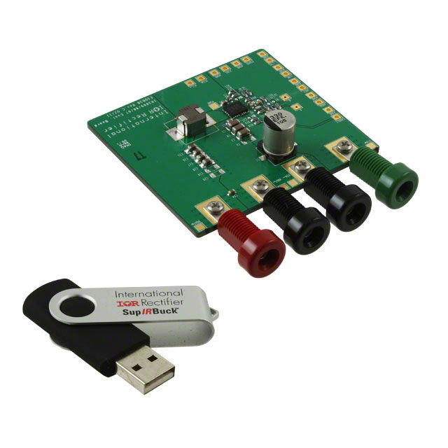
ICGOO电子元器件商城为您提供IRDC3897由International Rectifier设计生产,在icgoo商城现货销售,并且可以通过原厂、代理商等渠道进行代购。 IRDC3897价格参考。International RectifierIRDC3897封装/规格:评估板 - DC/DC 与 AC/DC(离线)SMPS, IR3897 SupIRBuck® DC/DC, Step Down 1, Non-Isolated Outputs Evaluation Board。您可以下载IRDC3897参考资料、Datasheet数据手册功能说明书,资料中有IRDC3897 详细功能的应用电路图电压和使用方法及教程。
IRDC3897 是英飞凌(Infineon Technologies)推出的一款评估板,主要用于 DC/DC 和 AC/DC(离线)开关电源(SMPS)的设计和测试。该评估板的核心是基于 Infineon 的 CoolMOS™ 或 OptiMOS™ 系列功率 MOSFET 以及相关驱动器 IC,适用于高效率、高性能的电源转换场景。以下是 IRDC3897 的主要应用场景:

 1. 消费电子设备
   - 电视电源:支持大屏幕电视的高效电源管理,提供稳定的电压输出。
   - 笔记本电脑适配器:用于设计高效的笔记本电脑充电器,满足快充需求。
   - 家用电器:如冰箱、洗衣机等需要稳定电源输入的家电产品。

 2. 工业应用
   - 工业电源:为工业设备提供高效、可靠的直流电源,例如 PLC 控制器或传感器供电。
   - 通信基站电源:支持电信行业的基站设备,确保其在不同负载条件下的稳定性。
   - 电机驱动电源:为工业电机驱动器提供高效的电源转换解决方案。

 3. 服务器与数据中心
   - 服务器电源模块:优化服务器内部电源管理,提高整体能效,降低散热需求。
   - 不间断电源(UPS):用于设计高效的 UPS 系统,确保关键设备在断电情况下的持续运行。

 4. 汽车电子
   - 车载充电器(OBC):支持电动车或混合动力车的车载充电器设计,实现快速充电和高效能量转换。
   - DC/DC 转换器:用于车内低压系统(如 12V 或 48V 系统)的电源管理。

 5. 可再生能源
   - 太阳能逆变器:用于光伏系统的 DC/AC 转换,提高能量转换效率。
   - 储能系统电源管理:为电池储能系统提供高效、稳定的电源转换方案。

 技术优势
- 高效率:采用先进的功率半导体技术,减少能量损耗。
- 紧凑设计:评估板结构紧凑,便于集成到各种设备中。
- 灵活性:支持多种拓扑结构(如反激式、正激式、LLC 等),适应不同的应用需求。
- 保护功能:内置过压、过流、短路等保护机制,提升系统可靠性。

通过 IRDC3897 评估板,工程师可以快速验证设计方案,优化电路参数,并缩短产品开发周期,特别适合对效率和可靠性要求较高的电源应用领域。
| 参数 | 数值 |
| 产品目录 | 编程器,开发系统半导体 |
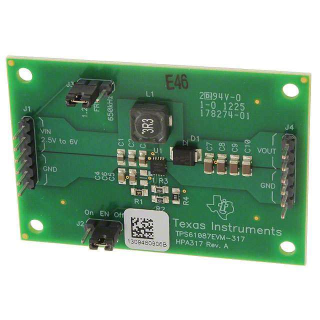
| 描述 | BOARD EVAL SUPIRBUCK IR3897电源管理IC开发工具 Design Kit POL IC |
| 产品分类 | |
| 品牌 | International Rectifier |
| 产品手册 | |
| 产品图片 |
|
| rohs | 否含铅 / 不符合限制有害物质指令(RoHS)规范要求 |
| 产品系列 | 电源管理IC开发工具,International Rectifier IRDC3897SupIRBuck™ |
| 数据手册 | |
| 产品型号 | IRDC3897 |
| 主要用途 | DC/DC,步降 |
| 产品 | Evaluation Boards |
| 产品培训模块 | http://www.digikey.cn/PTM/IndividualPTM.page?site=cn&lang=zhs&ptm=25926http://www.digikey.cn/PTM/IndividualPTM.page?site=cn&lang=zhs&ptm=26250 |
| 产品种类 | 电源管理IC开发工具 |
| 使用的IC/零件 | IR3897 |
| 功率-输出 | - |
| 商标 | International Rectifier |
| 封装 | Tube |
| 工具用于评估 | IR3897 |
| 工厂包装数量 | 1 |
| 所含物品 | 板 |
| 板类型 | 完全填充 |
| 标准包装 | 1 |
| 特色产品 | http://www.digikey.cn/product-highlights/cn/zh/international-rectifier-supirbuck-gen3-regulators/2366 |
| 电压-输入 | 12V |
| 电压-输出 | 1.2V |
| 电流-输出 | 4A |
| 稳压器拓扑 | 降压 |
| 类型 | Voltage Regulators - Switching Regulators |
| 输入电压 | 12 V |
| 输出和类型 | 1,非隔离 |
| 输出电压 | 1.2 V |
| 频率-开关 | 600kHz |


- 商务部:美国ITC正式对集成电路等产品启动337调查
- 曝三星4nm工艺存在良率问题 高通将骁龙8 Gen1或转产台积电
- 太阳诱电将投资9.5亿元在常州建新厂生产MLCC 预计2023年完工
- 英特尔发布欧洲新工厂建设计划 深化IDM 2.0 战略
- 台积电先进制程称霸业界 有大客户加持明年业绩稳了
- 达到5530亿美元!SIA预计今年全球半导体销售额将创下新高
- 英特尔拟将自动驾驶子公司Mobileye上市 估值或超500亿美元
- 三星加码芯片和SET,合并消费电子和移动部门,撤换高东真等 CEO
- 三星电子宣布重大人事变动 还合并消费电子和移动部门
- 海关总署:前11个月进口集成电路产品价值2.52万亿元 增长14.8%
PDF Datasheet 数据手册内容提取
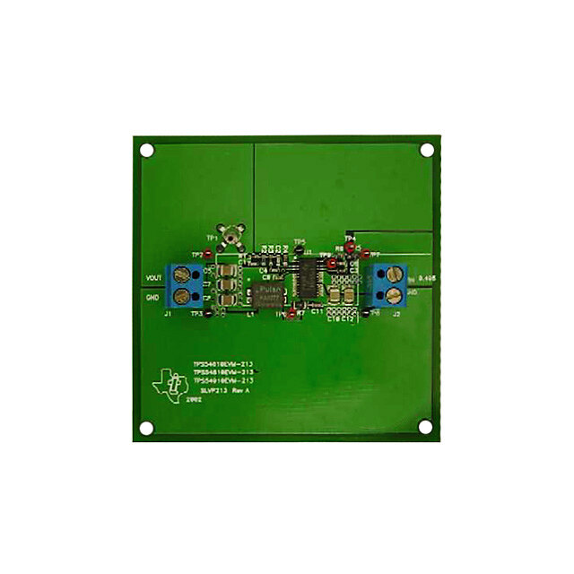
IRDC3897-P1V2 SupIRBuck TM USER GUIDE FOR IR3897 EVALUATION BOARD 1.2Vout DESCRIPTION Output over-current protection function is The IR3897 is a synchronous buck implemented by sensing the voltage developed converter, providing a compact, high across the on-resistance of the synchronous performance and flexible solution in a small Mosfet for optimum cost and performance and 4mmX 5 mmPower QFN package. thecurrentlimit is thermally compensated. Key features offered by the IR3897 include This user guide contains the schematic and bill internal Digital Soft Start/Soft Stop, precision of materials for the IR3897 evaluation board. 0.5Vreference voltage, Power Good, The guide describes operation and use of the thermal protection, programmable switching evaluation board itself. Detailed application frequency, Enable input, input under-voltage information for IR3897 is available in the lockout for proper start-up, enhanced line/ IR3897 datasheet. load regulation with feed forward, external frequency synchronization with smooth clocking, internal LDO and pre-bias start- up. BOARD FEATURES • V = +12V (+ 13.2V Max) in •V = +1.2V @ 0- 4A out • F =600kHz s • L= 1.5uH • C = 2x10uF (ceramic 1206) + 1X330uF (electrolytic) in • C =4x22uF (ceramic 0805) out 12/5/2012 1
IRDC3897-P1V2 CONNECTIONS and OPERATING INSTRUCTIONS A well regulated +12V input supply should be connected to VIN+ and VIN-. A maximum of 4A load should be connectedtoVOUT+ and VOUT-. The inputsand outputconnectionsoftheboard arelisted in Table I. IR3897 has only one input supply and internal LDO generatesVcc fromVin. Ifoperation with external Vcc is required, then R15 can be removed and external Vcc can be applied between Vcc+ and Vcc- pins. Vin pin and Vcc/LDO_Outpins should be shortedtogetherforexternal Vcc operation. The output can track voltage at the Vp pin. For this purpose, Vref pin is to be connected to ground (use zero ohm resistor for R21). The value of R14 and R20 can be selected to provide the desired tracking ratio between outputvoltage and thetrackinginput. Table I. Connections Connection Signal Name VIN+ Vin (+12V) VIN- Ground of Vin Vout+ Vout(+1.2V) Vout- Ground for Vout Vcc+ Vcc/ LDO_Out Pin Vcc- Ground for Vcc input Enable Enable PGood Power Good Signal AGnd Analog ground LAYOUT The PCB is a 4-layer board (2.23”x2”) using FR4 material. All layers use 2 Oz. copper. The PCB thickness is 0.062”. The IR3897 and other major power components are mounted on the top side of the board. Power supply decoupling capacitors, the bootstrap capacitor and feedback components are located close to IR3897. The feedback resistors are connected to the output at the point of regulation and are located close to the SupIRBuck IC. To improve efficiency, the circuit board is designed to minimize the length oftheon-board power groundcurrentpath. 12/5/2012 2
IRDC3897-P1V2 Connection Diagram Vin Gnd Gnd Vout Enable VDDQ Top View Vref Sync S-Ctrl AGnd PGood Vsns Vcc+ Vcc- Bottom View Fig.1: Connection Diagram of IR3899/98/97Evaluation Boards 12/5/2012 3
IRDC3897-P1V2 Fig.2: Board Layout-Top Layer Single point connection between AGnd and PGnd Fig.3: Board Layout-Bottom Layer 12/5/2012 4
IRDC3897-P1V2 Fig.4: Board Layout-Mid Layer 1 Fig.5: Board Layout-Mid Layer 2 12/5/2012 5
IRDC3897-P1V2 V) 2 1. VinVin+1 Vin+1 C2C1+N/SVin-330uF/25V1 1206Vin-1 Vout+ (Vout1 Vout+1 C14C15C160.1uFVout-22uF22uF1 Vout-1 C3N/S mic: C17 22uF C410uF cera C18 22uF C510uF Input C19C20 N/SN/S C6N/A C27 N/S d C28 N/S +C36N/S oar b C29C30 N/SN/S C35+N/S R50 0 ohm ation u l a v e 7 R15 0 ohm L1 1.5uH R11 3.32K R122.37K R6 1ohm B IR389 R18 49.9KVCC R29N/S C321.0uFC24R10 0 ohm0.1uF41 to13oPVinBC70.1uF89712N38703SW PGND 11sD1PGndnNVsnssGV 8711 C25R7N/SN/A C8R4 100 ohm2200pF R2 13.32K20 R3A2.37K hematicofthe able 9 enlibVanE IR3TUO_ODdLo/ocGcPV 7 Sc En 1 C37 N/S 512 FERVFB COMP Gnd Rt_Sync Vp S_Ctrl 01 VCC C232.2uF g.6: EF R19 7.5K U1 1 3 4 5 16 S_Ctrl6 1 R13 0 ohm Fi VR 1 C12 100pF F C26 10nF R21N/S C11 120p R1 3.01k SYNC 1 R939.2K C C VDDQAgnd 11 R140 ohm R28C10N/SN/A Vcc+Vcc-V 11 R17PGood49.9K 1 12/5/2012 6
IRDC3897-P1V2 Bill of Materials Item Qty Part Reference Value Description Manufacturer Part Number 1 1 C1 330uF SMD Electrolytic F size 25V 20% Panasonic EEV-FK1E331P 2 2 C4 C5 10uF 1206, 25V, X5R, 20% TDK C3216X5R1E106M GRM188R71E104KA0 3 3 C7 C14 C24 0.1uF 0603, 25V, X7R, 10% Murata 1B 4 1 C12 100pF 0603,50V,NP0, 5% Murata GRM1885C1H101JA01D 2200p GRM188R71H222KA0 5 1 C8 F 0603,50V,X7R Murata 1B GRM1885C1H121JA0 0603, 50V, NP0, 5% Murata 6 1 C11 120pF 1D 7 4 C15 C16 C17 C18 22uF 0805, 6.3V, X5R, 20% TDK C2012X5R0J226M 8 1 C23 2.2uF 0603, 16V, X5R, 20% TDK C1608X5R1C225M GRM188R71E103KA0 0603, 25V, X7R, 10% 9 1 C26 10nF Murata 1J GRM188R61E105KA1 0603, 25V, X5R, 10% 10 1 C32 1.0uF Murata 2D 11 1 L1 1.5uH SMD 7.05x6.6x4.8mm,6.7mΩ Cyntec PCMB065T-1R5MS 12 1 R1 3.01K Thick Film, 0603,1/10W,1% Panasonic ERJ-3EKF3011V 13 2 R2 R11 3.32K Thick Film, 0603,1/10W,1% Panasonic ERJ-3EKF3321V 14 2 R3 R12 2.37K Thick Film, 0603,1/10W,1% Panasonic ERJ-3EKF2371V 15 1 R4 100 Thick Film, 0603,1/10W,1% Panasonic ERJ-3EKF1000V 16 1 R6 20 Thick Film, 0603,1/10W,1% Panasonic ERJ-3EKF20R0V 17 1 R9 39.2K Thick Film, 0603,1/10W,1% Panasonic ERJ-3EKF3922V R10 R13 R14 R15 Thick Film, 0603,1/10W 18 5 R50 0 Panasonic ERJ-3GEY0R00V 19 2 R17 R18 49.9K Thick Film, 0603,1/10W,1% Panasonic ERJ-3EKF4992V 20 1 R19 7.5K Thick Film, 0603,1/10W,1% Panasonic ERJ-3EKF7501V IR389 21 1 U1 7 PQFN 4x5mm IR IR3897MPBF 12/5/2012 7
IRDC3897-P1V2 TYPICAL OPERATING WAVEFORMS Vin=12.0V, Vo=1.2V, Io=0-4A, Room Temperature, no airflow Fig. 7: Start up at 4A Load Fig. 8: Start up at 4A Load, Ch :V , Ch :V , Ch :P Ch :Enable Ch :V , Ch :V , Ch :Vcc, Ch :P 1 in 2 o 3 Good 4 1 in 2 o 3 4 Good Fig. 9: Start up with 1V Pre Bias , 0A Load, Fig. 10: Output Voltage Ripple, 4A load Ch :V Ch : V 2 o 2 out , Fig. 12: Short circuit (Hiccup) Recovery Fig. 11: Inductor node at 4A load Ch :V , Ch4:Iout Ch :LX 2 out 2 12/5/2012 8
IRDC3897-P1V2 TYPICAL OPERATING WAVEFORMS Vin=12.0V, Vo=1.2V, Io=0-4A, Room Temperature, no air flow Fig. 13: Transient Response, 2.0A to 4A step Ch :V Ch4-Iout 2 out 12/5/2012 9
IRDC3897-P1V2 TYPICAL OPERATING WAVEFORMS Vin=12.0V, Vo=1.2V, Io=0-4A, Room Temperature, no air flow Fig. 14: Bode Plot at 4A load shows a bandwidth of 112.6KHz and phase margin of 52.4 degrees 12/5/2012 10
IRDC3897-P1V2 TYPICAL OPERATING WAVEFORMS Vin=12.0V, Vo=1.2V, Io=0-4A, Room Temperature, no air flow Fig (15) Soft start and soft stop using S_Ctrl pin Fig (16) Feed Forward for Vin change from 7 to 16V and back to 7V Ch -Vout Ch -Vin 2 4 12/5/2012 11
IRDC3897-P1V2 TYPICAL OPERATING WAVEFORMS Vin=12.0V, Vo=1.2V, Io=0-4A, Room Temperature, no air flow 90 88 86 84 %) 82 y ( c n 80 e ci Effi 78 76 74 72 70 0.4 0.8 1.2 1.6 2 2.4 2.8 3.2 3.6 4 Load Current (A) Fig.17: Efficiency versus load current 0.775 0.700 0.625 W) 0.550 n( o ati 0.475 p si s Di 0.400 r e w o 0.325 P 0.250 0.175 0.100 0.4 0.8 1.2 1.6 2 2.4 2.8 3.2 3.6 4 Load Current (A) Fig.18: Power loss versus load current 12/5/2012 12
IRDC3897-P1V2 THERMAL IMAGES Vin=12.0V, Vo=1.2V, Io=0-4A, Room Temperature, No Air flow Fig. 19: Thermal Image of the board at 4A load Test point 1 is IR3897 Test point 2 is inductor 12/5/2012 13
IRDC3897-P1V2 PCB METAL AND COMPONENT PLACEMENT Evaluations have shown that the best overall performance is achieved using the substrate/PCB layout as shown in following figures. PQFN devices should be placed to an accuracy of 0.050mm on both X and Y axes. Self-centering behavior is highly dependent on solders and processes, and experiments should be run to confirm the limits of self-centering on specific processes. For further information, please refer to “SupIRBuck™ Multi-Chip Module (MCM) Power Quad Flat No-Lead (PQFN) Board Mounting Application Note.” (AN1132) Figure 20: PCB Metal Pad Spacing (all dimensions in mm) 12/5/2012 14
IRDC3897-P1V2 SOLDER RESIST IR recommends that the larger Power or Land Area pads are Solder Mask Defined (SMD.) This allows the underlying Copper traces to be as large as possible, which helps in terms of current carrying capability and device cooling capability. When using SMD pads, the underlying copper traces should be at least 0.05mm larger (on each edge) than the Solder Mask window, in order to accommodate any layer to layer misalignment. (i.e. 0.1mm in X & Y.) However, for the smaller Signal type leads around the edge of the device, IR recommends that these are Non Solder Mask Defined or Copper Defined. When using NSMD pads, the Solder Resist Window should be larger than the Copper Pad by at least 0.025mm on each edge, (i.e. 0.05mm in X&Y,) in order to accommodate any layer to layer misalignment. Ensure that the solder resist in-between the smaller signal lead areas are at least 0.15mm wide, due to the high x/y aspect ratio of the solder mask strip. Figure 21: Solder resist 12/5/2012 15
IRDC3897-P1V2 STENCIL DESIGN Stencils for PQFN can be used with thicknesses of 0.100-0.250mm (0.004-0.010"). Stencils thinner than 0.100mm are unsuitable because they deposit insufficient solder paste to make good solder joints with the ground pad; high reductions sometimes create similar problems. Stencils in the range of 0.125mm-0.200mm (0.005-0.008"), with suitable reductions, give the best results. Evaluations have shown that the best overall performance is achieved using the stencil design shown in following figure. This design is for a stencil thickness of 0.127mm (0.005").The reduction should be adjusted for stencils of other thicknesses. Figure 22: Stencil Pad Spacing (all dimensions in mm) 12/5/2012 16
IRDC3897-P1V2 PACKAGE INFORMATION Figure 23: Package Dimensions IR WORLD HEADQUARTERS: 233 Kansas St., El Segundo, California 90245, USA Tel: (310) 252-7105 TAC Fax: (310) 252-7903 This product has been designed and qualified for the Industrial market Visit us at www.irf.com for sales contact information Data and specifications subject to change without notice.12/11 12/5/2012 17