ICGOO在线商城 > 集成电路(IC) > PMIC - LED 驱动器 > UCC28810D

 Datasheet下载
- 型号: UCC28810D
- 制造商: Texas Instruments
- 库位|库存: xxxx|xxxx
- 要求:
| 数量阶梯 | 香港交货 | 国内含税 |
| +xxxx | $xxxx | ¥xxxx |
查看当月历史价格
查看今年历史价格
UCC28810D产品简介:
ICGOO电子元器件商城为您提供UCC28810D由Texas Instruments设计生产,在icgoo商城现货销售,并且可以通过原厂、代理商等渠道进行代购。 UCC28810D价格参考¥2.50-¥6.21。Texas InstrumentsUCC28810D封装/规格:PMIC - LED 驱动器, LED 驱动器 IC 1 输出 交直流离线开关 反激,SEPIC,降压,升压 Triac 调光 750mA 8-SOIC。您可以下载UCC28810D参考资料、Datasheet数据手册功能说明书,资料中有UCC28810D 详细功能的应用电路图电压和使用方法及教程。
UCC28810D 是 Texas Instruments(德州仪器)推出的一款 PMIC - LED 驱动器,主要用于高效驱动LED照明系统。以下是其主要应用场景:

 1. 智能照明
   - UCC28810D 适用于智能照明系统,如智能家居中的可调光LED灯、环境感应灯等。它支持高效率的功率转换,能够根据需求动态调整LED亮度,同时保持低功耗和高稳定性。
   - 支持DALI(数字可寻址照明接口)或PWM调光协议,广泛用于家庭、办公室和商业场所的智能照明解决方案。

 2. 户外照明
   - 该芯片适用于户外LED路灯、庭院灯和景观灯等场景。它具有良好的热管理和高效的功率转换能力,能够在极端温度条件下稳定运行。
   - 提供恒流输出,确保LED在不同电压下保持一致的亮度,延长灯具寿命。

 3. 工业照明
   - 在工厂、仓库等工业环境中,UCC28810D 可用于高亮度LED工矿灯、面板灯和筒灯的设计。其高效率和可靠性满足了工业照明对长时间稳定运行的要求。
   - 支持宽输入电压范围(通常为9V至75V),适应复杂的供电环境。

 4. 汽车照明
   - UCC28810D 可用于汽车内部和外部照明,例如尾灯、刹车灯、转向灯以及车内氛围灯。其高效能设计有助于减少能量损耗,提升车辆的整体能效。
   - 具备短路保护、过温保护等功能,增强了系统的安全性和耐用性。

 5. 显示屏背光
   - 在液晶显示器(LCD)和电视背光应用中,UCC28810D 能够提供精确的电流控制,确保屏幕亮度均匀且无闪烁。
   - 支持多串LED驱动,适合大尺寸显示屏的应用需求。

 6. 应急照明
   - UCC28810D 的高可靠性和低功耗特性使其非常适合应急照明设备,如备用电源供电的LED灯具。即使在电池供电模式下,也能保证稳定的亮度输出。

总之,UCC28810D 凭借其高效能、高稳定性和多功能特性,在各种LED照明领域都有广泛的应用前景,尤其适合需要高精度电流控制和节能设计的场景。
| 参数 | 数值 |
| 产品目录 | 集成电路 (IC)光电子产品 |
| 描述 | IC LED DRIVER LINEAR 8-SOICLED照明驱动器 LED Lighting Pwr Controller |
| 产品分类 | |
| 品牌 | Texas Instruments |
| 产品手册 | |
| 产品图片 |
|
| rohs | 符合RoHS无铅 / 符合限制有害物质指令(RoHS)规范要求 |
| 产品系列 | LED照明电子器件,LED照明驱动器,Texas Instruments UCC28810D- |
| 数据手册 | |
| 产品型号 | UCC28810D |
| 产品培训模块 | http://www.digikey.cn/PTM/IndividualPTM.page?site=cn&lang=zhs&ptm=22866 |
| 产品目录页面 | |
| 产品种类 | LED照明驱动器 |
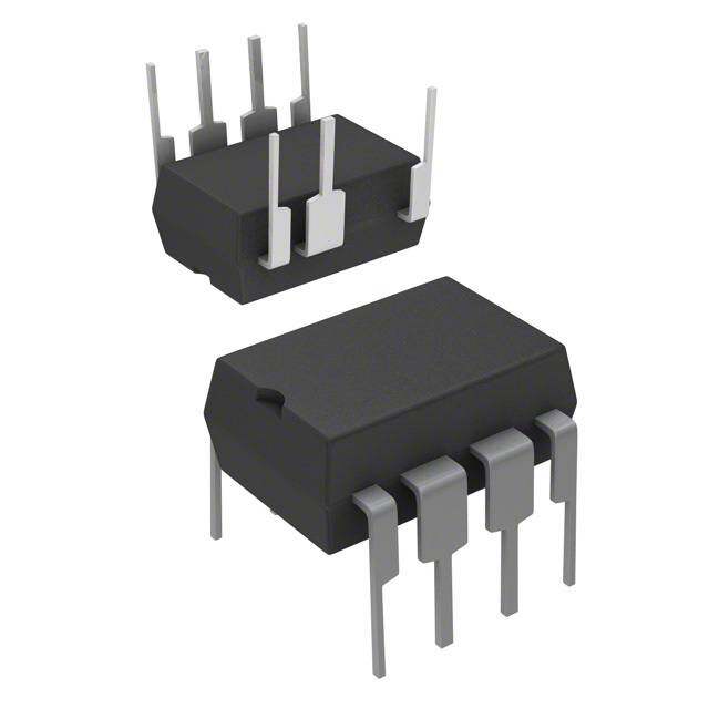
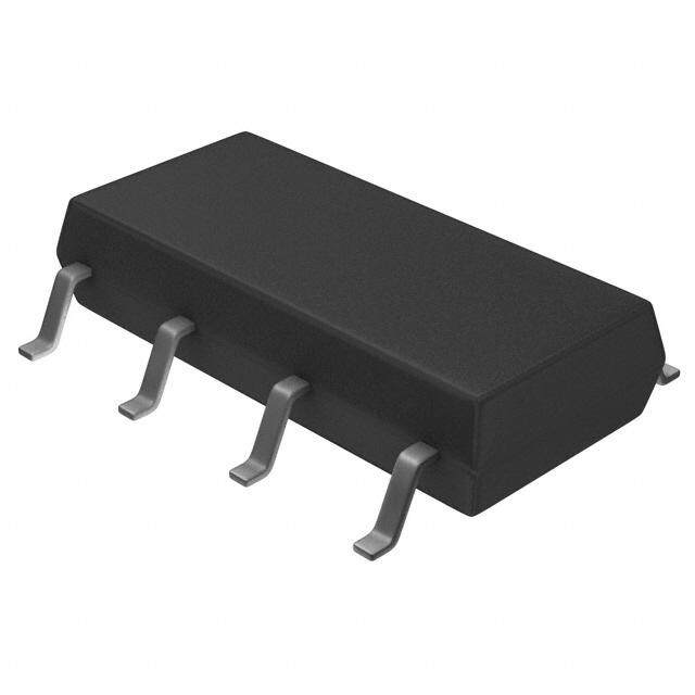
| 供应商器件封装 | 8-SOIC |
| 其它名称 | 296-27162-5 |
| 内部驱动器 | 无 |
| 制造商产品页 | http://www.ti.com/general/docs/suppproductinfo.tsp?distId=10&orderablePartNumber=UCC28810D |
| 功率耗散 | 150 W |
| 包装 | 管件 |
| 单位重量 | 72.600 mg |
| 商标 | Texas Instruments |
| 安装类型 | 表面贴装 |
| 安装风格 | SMD/SMT |
| 封装 | Tube |
| 封装/外壳 | 8-SOIC(0.154",3.90mm 宽) |
| 封装/箱体 | SOIC-8 |
| 工作温度 | -40°C ~ 105°C |
| 工作频率 | 5 kHz to 250 kHz |
| 工厂包装数量 | 75 |
| 恒压 | - |
| 恒流 | - |
| 拓扑 | PWM |
| 拓扑结构 | Boost, Buck, Flyback |
| 最大工作温度 | + 105 C |
| 最大电源电流 | 6 mA |
| 最小工作温度 | - 40 C |
| 标准包装 | 75 |
| 特色产品 | http://www.digikey.com/product-highlights/cn/zh/texas-instruments-national-winning-combo/366 |
| 电压-电源 | 18V |
| 电压-输出 | - |
| 类型 | Inductive |
| 类型-初级 | 通用 |
| 类型-次级 | 高亮度 LED(HBLED),白色 LED |
| 系列 | UCC28810 |
| 输入电压 | 16.4 V to 18 V |
| 输出数 | 1 |
| 输出电流 | 750 mA |
| 输出端数量 | 1 Output |
| 输出类型 | Current Mode |
| 频率 | - |


- 商务部:美国ITC正式对集成电路等产品启动337调查
- 曝三星4nm工艺存在良率问题 高通将骁龙8 Gen1或转产台积电
- 太阳诱电将投资9.5亿元在常州建新厂生产MLCC 预计2023年完工
- 英特尔发布欧洲新工厂建设计划 深化IDM 2.0 战略
- 台积电先进制程称霸业界 有大客户加持明年业绩稳了
- 达到5530亿美元!SIA预计今年全球半导体销售额将创下新高
- 英特尔拟将自动驾驶子公司Mobileye上市 估值或超500亿美元
- 三星加码芯片和SET,合并消费电子和移动部门,撤换高东真等 CEO
- 三星电子宣布重大人事变动 还合并消费电子和移动部门
- 海关总署:前11个月进口集成电路产品价值2.52万亿元 增长14.8%


PDF Datasheet 数据手册内容提取
UCC28810 UCC28811 www.ti.com.............................................................................................................................................................................................. SLUS865–OCTOBER2008 LED LIGHTING POWER CONTROLLER FEATURES APPLICATIONS 1 • TransitionModeControllerforLow • ACInputGeneralLightingApplicationsUsing ImplementationCostofACInputLEDLighting HBLEDs Applications • Industrial,CommercialandResidential • ImplementsSingleStagePowerFactor LightingFixtures CorrectedLEDDriver • OutdoorLighting:Street,Roadway,Parking, ConstructionandOrnamentalLEDLighting • EnhancedTransientResponseWithSlew-Rate Fixtures Comparator • InterfaceswithTraditionalWallDimmers DESCRIPTION • AccurateInternalV forTightOutput REF The UCC28810 and UCC28811 are general lighting Regulation power controllers for low to medium power lumens • TwoUVLOOptions applications requiring power factor correction and • OvervoltageProtection(OVP),Open-Feedback EMC compliance. It is designed for controlling a flyback, buck or boost converter operating in critical ProtectionandEnableCircuits conduction mode. It features a transconductance • ±750-mAPeakGateDriveCurrent voltage amplifier for feedback error processing, a • LowStart-UpandOperatingCurrents simple current reference generator for generating a • Lead(Pb)-FreePackages current command proportional to the input voltage, a current-sense (PWM) comparator, PWM logic and a totem-poledriverfordrivinganexternalFET. SIMPLIFIED APPLICATION DIAGRAM Bias UCC28810 1 VSENSE VDD 8 2 EAOUT GDRV 7 Low Pass Filter 3 VINS GND 6 LED 4 ISENSE TZE 5 Current Triac Dimming Sense Detect Bias + + UDG-08120 1 Pleasebeawarethatanimportantnoticeconcerningavailability,standardwarranty,anduseincriticalapplicationsofTexas Instrumentssemiconductorproductsanddisclaimerstheretoappearsattheendofthisdatasheet. PRODUCTIONDATAinformationiscurrentasofpublicationdate. Copyright©2008,TexasInstrumentsIncorporated Products conform to specifications per the terms of the Texas Instruments standard warranty. Production processing does not necessarilyincludetestingofallparameters.
UCC28810 UCC28811 SLUS865–OCTOBER2008.............................................................................................................................................................................................. www.ti.com DESCRIPTION (CONTINUED) In the critical conduction mode operation, the PWM circuit is self-oscillating with the turn-on being governed by a transformer zero energy detector (TZE pin) and the turn-off being governed by the current sense comparator. Additionally, the controller provides features such as peak current limit, restart timer, overvoltage protection (OVP),andenable. The efficient system performance is attained by incorporation of zero power detect function which allows the controller output to shut down at light load conditions without running into overvoltage. The device also features an innovative slew rate enhancement circuit which improves the large signal transient performance of the voltage error amplifier. The low start-up and operating currents of the device result in low power consumption and ease of start-up. The highly-accurate internal bandgap reference leads to tight regulation of the output voltage in normal and OVP conditions, resulting in higher system reliability. The enable comparator ensures that the controllerisoffifthefeedbacksensepathisbrokenoriftheinputvoltageisverylow. There are two key parametric differences between UCC28810 and UCC28811, the UVLO turn-on threshold and theg amplifiersourcecurrent.TheUVLOturn-onthresholdofthe UCC28810 is 15.8 V and for the UCC28811 it M is 12.5 V. The g amplifier source current for UCC28810 is typically 1.3 mA, and for the UCC28811 it is 300m A. M The higher UVLO turn-on threshold of the UCC28810 allows quicker and easier start-up with a smaller VDD capacitance while the lower UVLO turn-on threshold of UCC28811 allows operation of the critical conduction mode controller to be easily controlled by the downstream PWM controller in two-stage power converters. The UCC28810 g amplifier also provides a full 1.3-mA typical source current for faster start-up and improved M transient response when the output is low either at start-up or during transient conditions. The UCC28811 is suitable for applications such as street lights and larger area luminaires where a two-stage power conversion is needed. The UCC28810 is suitable for applications such as commercial or residential retrofit luminaires where there is no down-stream PWM conversion and the advantages of smaller VDD capacitor and improved transient responsecanberealized. Devices are available in the industrial temperature range of –40°C to 105°C. Package offering is an 8-pin SOIC (D)package. ORDERINGINFORMATION(1) UVLOTHRESHOLD g AMPLIFIER T =T VOLTAGE(V) SOUMRCECURRENT PACKAGE PIN SUPPLY ORDERABLE A J COUNT DEVICENUMBER ON OFF (m A) Tubeof80 UCC28810D 15.8 9.7 –1300 Reelof2500 UCC28810DR –40°Cto105°C D 8 Tubeof80 UCC28811D 12.5 9.7 –300 Reelof2500 UCC28811DR (1) D(SOIC-8)packageisavailabletapedandreeled.AddRsuffixtodevicetype(e.g.UCC28810DR)toorderquantitiesof2,500devices perreel. ABSOLUTE MAXIMUM RATINGS(1) VALUE UNIT VDD(Internallyclamped) 20 Inputvoltage VSENSE,VINS,ISENSE 5 V Minimuminput VSENSE,VINS,ISENSE –5 voltage VDD 30 Inputcurrent mA TZE ±10 Outputcurrent GDRV ±750 mA Outputvoltage GDRV –5 V Tstg Storagetemperature –55to150 TJ Operatingtemperature –65to150 °C Solderingtemperature 300 (1) PermanentdevicedamagemayoccurifAbsoluteMaximumRatingsareexceeded.Exposuretoconditionsbeyondtheoperational limitsforextendedperiodsoftimemayaffectdevicereliability.Currentsarepositiveinto,andnegativeoutofthespecifiedterminal. 2 SubmitDocumentationFeedback Copyright©2008,TexasInstrumentsIncorporated ProductFolderLink(s):UCC28810UCC28811
UCC28810 UCC28811 www.ti.com.............................................................................................................................................................................................. SLUS865–OCTOBER2008 PACKAGE DISSIPATION RATINGS(1) PACKAGE THERMALIMPEDANCEJUNCTION-TO-AMBIENT(°C/W) Plastic8-PinSmallOutline 150 (1) TIdevicepackagesaremodeledandtestedforthermalperformanceusingprintedcircuitboard designsoutlinedinJEDECstandardsJESD51-3andJESD51-7. Copyright©2008,TexasInstrumentsIncorporated SubmitDocumentationFeedback 3 ProductFolderLink(s):UCC28810UCC28811
UCC28810 UCC28811 SLUS865–OCTOBER2008.............................................................................................................................................................................................. www.ti.com ELECTRICAL CHARACTERISTICS –40°C≤T =T ≤105°C,V =12V ,C =0.1-m FfromVDDtoGND,allvoltagesarewithrespecttoGND. A J VDD DC GDRV PARAMETER TESTCONDITIONS MIN TYP MAX UNIT SUPPLY V Operatingvoltage 18 VDD V Shuntvoltage I =25mA 18 19 20 VDD Supplycurrent,off V =V turn-onthreshold–300mV 75 125 m A VDD VDD Supplycurrent,disabled V =0.5V 2 4 VSENSE I Supplycurrent,on 75kHz,C =0nF 4 6 mA VDD GDRV Supplycurrent,dynamicoperating 75kHz,C =1nF 5 7 GDRV UVLO UCC28810 15.4 15.8 16.4 VDDturn-onthreshold UCC28811 12.0 12.5 13.0 V VDDturn-offthreshold 9.4 9.7 10.0 UCC28810 5.8 6.3 6.8 V UVLOhysteresis V UVLO UCC28811 2.3 2.8 3.3 VOLTAGEAMPLIFIER(VSENSE) V Internalvoltagereference 2.45 2.50 2.55 V REF I Inputbiascurrent 0.5 m A BIAS EAOUThigh V =2.1V 4.5 5.5 V VSENSE EAOUTlow V =2.55V 1.80 2.45 V VSENSE g Transconductance T =25°C,V =3.5V 60 90 130 m S M J EAOUT UCC28810 –0.2 –1.0 mA I Sourcecurrent V =2.1V,V =3.5V EAOUT,SRC UCC28811 VSENSE EAOUT –200 –300 –400 m A I Sinkcurrent V =2.1V,V =3.5V 0.2 1.0 mA EAOUT,SNK VSENSE EAOUT OVERVOLTAGEPROTECTION/ENABLE(VSENSE) V + V V UCC28810 VREF VREF VREF 0.165 +0.190 +0.210 V Overvoltagereference V OV(ref) V + V + V + UCC28811 VREF VREF VREF 0.150 0.180 0.210 UCC28810 175 200 225 Hysteresis mV UCC28811 150 180 210 UCC28810 0.62 0.67 0.72 Enablethreshold V UCC28811 0.18 0.23 0.28 Enablehysteresis 0.05 0.10 0.20 V CURRENTREFERENCEGENERATOR K Currentreferencegeneratorgainconstant V =0.5V,V =3.5V 0.43 0.65 0.87 1/V VINS EAOUT Dynamicinputrange,V INPUT 0to2.5 0to3.5 V VINS 2.5to 2.5to V Erroramplifierdynamicinputrange V EAOUT 3.8 4.0 Inputbiascurrent,VINS 0.1 1.0 m A 4 SubmitDocumentationFeedback Copyright©2008,TexasInstrumentsIncorporated ProductFolderLink(s):UCC28810UCC28811
UCC28810 UCC28811 www.ti.com.............................................................................................................................................................................................. SLUS865–OCTOBER2008 ELECTRICAL CHARACTERISTICS (continued) –40°C≤T =T ≤105°C,V =12V ,C =0.1-m FfromVDDtoGND,allvoltagesarewithrespecttoGND. A J VDD DC GDRV PARAMETER TESTCONDITIONS MIN TYP MAX UNIT ZEROPOWER V Zeropowercomparatorthreshold(1) 2.1 2.3 2.5 V EAOUT TRANSFORMERZEROENERGYDETECT Inputthreshold(risingedge)(1) 1.00 1.25 1.80 V Hysteresis(1) 250 350 450 mV Inputhighclamp I =3mA 5 6 V TZE Inputlowclamp I =–3mA 0.30 0.65 0.90 V TZE t Restarttimedelay 200 400 m s RSRT CURRENTSENSECOMPARATOR I Inputbiascurrent V =0V 0.1 1.0 m A BIAS ISENSE Inputoffsetvoltage(1) –10 10 mV t Delaytooutput ISENSEtoGDRV 300 400 ns DLY Maximumcurrentsensethresholdvoltage 1.55 1.70 1.80 V PFCGATEDRIVER R GDRVpullupresistance I =–125mA 5 12 Ω PULLUP GDRV R GDRVpulldownresistance I =125mA 2 10 Ω PULLDN GDRV t GDRVoutputrisetime C =1nF,R =10Ω 25 75 ns RISE GDRV GRDV t GDRVoutputfalltime C =1nF,R =10Ω 10 50 ns FALL GDRV GRDV (1) Ensuredbydesign.Notproductiontested. Copyright©2008,TexasInstrumentsIncorporated SubmitDocumentationFeedback 5 ProductFolderLink(s):UCC28810UCC28811
UCC28810 UCC28811 SLUS865–OCTOBER2008.............................................................................................................................................................................................. www.ti.com Table1.PINDESCRIPTIONS TERMINAL I/O DESCRIPTION NAME NO. Outputofthetransconductanceerroramplifier.Theoutputcurrentcapabilityofthispinis10m Aundernormal conditions,butincreasesto1mAwhenthevoltageonVSENSErisesabove2.5V.TheEAOUTvoltageisoneof theinputstothecurrentreferencegenerator,withadynamicinputrangeof2.5Vto4.0V.Duringzeroenergyor EAOUT 2 O overvoltageconditions,thispingoesbelow2.5V,nominal.Whenitgoesbelow2.3V,thezeroenergydetect comparatorisactivatedwhichpreventsthegatedrivefromswitching.Loopcompensationcomponentsare connectedbetweenthispinandground,orcanbeconnecteddirectlytothecollectoroftheoptocouplerinisolated applications. Thedevicereferenceground.AllbypassingelementsareconnectedtotheGNDpinwiththeshortesttraces GND 6 – possible. Thegatedriveoutputdrivingtheflyback,buck,orboostswitch.Thisoutputiscapableofdeliveringupto750-mA GDRV 7 O peakcurrentsduringturn-onandturn-off.Anexternalgatedriveresistormaybeneededtolimitthepeakcurrent dependingupontheVDDvoltagebeingused.BelowtheUVLOthreshold,theoutputisheldlow. Thispinsensestheinstantaneousswitchcurrentintheexternalswitchandusesthissignalastheinternalrampfor thecurrentsensecomparator.Asmallinternalnoisefilterisprovided.Ifadditionalfilteringisneeded,anexternal R-Cfiltermaybeaddedtofurthersuppressnoisespikes.Aninternalclamponthecurrentreferencegenerator ISENSE 4 I outputterminatestheswitchingcycleifVISENSEexceeds1.7V.Aninternal75-mVoffsetisaddedtoISENSEsignal tolimitthezerocrossingdistortion.TheISENSEthresholdvoltageisapproximatelyequalto: V @0.67´(V -2.5V)´(V +75mV) ISENSE EAOUT VINS Thispinistheinputforthetransformerzeroenergydetectcomparator.Abiaswindingcanbeusedtosensethe transformerzeroenergy.ThetransitionisdetectedwhentheinductorcurrentfallstozeroandtheTZEinputgoes TZE 5 I low.InternalactiveclampsareprovidedtopreventTZEfromgoingbelowgroundorrisingtoohigh.Ifzeroenergyis notdetectedwithin400m s,arestarttimersetsthelatchandthegatedrivehigh. Thesupplyvoltageforthedevice.Thispinmustbebypassedwithahigh-frequencycapacitor(notlessthan0.1m F) andtieddirectlytoGNDwiththeshortesttracespossible.TheUCC28810hasawideUVLOhysteresis,typically 6.3V,whichallowsuseofalowervalueholdupcapacitoronVDD,resultinginfasterstartup.TheUCC28811hasa VDD 8 I narrowUVLOhysteresis,typically2.8V,andatypicalturn-onthresholdof12.5Vforapplicationswherethedevice needstobecontrolledbyadownstreamPWMcontroller.ThisnarrowerUVLOhysteresisrequiresalargervalue holdupcapacitor. Thispinsensestheinstantaneousregulatorinputvoltagethroughanexternalvoltagedivider.TheVINSvoltage VINS 3 I actsasoneoftheinputstothecurrentreferencegenerator.Therecommendedoperatingrangeis0Vto3.8Vat highline. Thispinistheinvertinginputtothetransconductanceamplifier,withanominalvalueof2.5V,andisalsotheinput totheOVPcomparator.PullingthispinbelowtheENABLEthresholdturnsofftheoutputswitching,providingthe VSENSE 1 I abilitytoexternallydisabletheconverter.Thisfunctionalsoprovidesfeedbackfaultprotection,ensuringnorunaway ifthefeedbackpathisopen.Whenusingtheinternalerroramplifier,thispinsensestheoutputvoltagethrougha voltagedivider. SOIC-8PACKAGE(TOPVIEW) VSENSE 1 8 VDD EAOUT 2 7 GDRV VINS 3 6 GND ISENSE 4 5 TZE 6 SubmitDocumentationFeedback Copyright©2008,TexasInstrumentsIncorporated ProductFolderLink(s):UCC28810UCC28811
UCC28810 UCC28811 www.ti.com.............................................................................................................................................................................................. SLUS865–OCTOBER2008 BLOCK DESCRIPTION BLOCKDIAGRAM V UVLO OVP REF V and 2.7/2.5V + REF + Init.Bias BiasReg 0.67/0.57V + Enable V REF 8 VDD 0.23/0.15V REF GOOD g VEA OVP M VSENSE 1 x CurrentSenseComparator 2.5V + K 7 GDRV x + R Q EAOUT 2 Current Reference S Q Generator VINS 3 6 GND ZeroEnergy RestartTimer 2.3V + Detect + 1.7/1.4V 40kW + ISENSE 4 5 TZE 75mV 5pF UDG-08130 UVLOandReferenceCircuit This circuitry generates a precision reference voltage used to obtain a tightly controlled UVLO threshold. In addition to generating a 2.5-V reference for the noninverting terminal of the g amplifier, it generates the M reference voltages for OVP, enable, zero energy detect and the current reference generator circuits. An internal railof7.5Visalsogeneratedtodrivealltheinternalcircuitry. ErrorAmplifier The voltage error amplifier in the UCC2881x is a transconductance amplifier with a typical transconductance value of 90m S. The advantage in using a transconductance amplifier is that the inverting input of the amplifier is solely determined by the external resistive-divider from the output voltage and not the transient behavior of the amplifieritself.ThisallowstheVSENSEpintobeusedforsensingovervoltageconditions. The sink and source capability of the error amplifier is approximately 10 m A during normal operation of the amplifier. But when the VSENSE pin voltage is beyond the normal operating conditions (V >1.05 × V , VSENSE REF V < 0.88 × V ), additional circuitry to enhance the slew-rate of the amplifier is activated. Enhanced VSENSE REF slew-rate of the compensation capacitor results in a faster start-up and transient response. This prevents the output voltage from drifting too high or too low, which can happen if the compensation capacitor were to be driven by the normal drive current of 10-m A. When VSENSE rises above the normal range, the enhanced sink current capability increases to 1 mA, nominal. When VSENSE falls below the normal range, the UCC28810 can source more than 1 mA and the UCC28811 sources approximately 300 m A. The limited source current in the UCC28811 helps to gradually increase the error voltage on the EAOUT pin preventing a step increase in line current. The actual rate of increase of the voltage on the EAOUT pin is dependent on the compensation network externallyconnectedtotheEAOUTpin. Copyright©2008,TexasInstrumentsIncorporated SubmitDocumentationFeedback 7 ProductFolderLink(s):UCC28810UCC28811
UCC28810 UCC28811 SLUS865–OCTOBER2008.............................................................................................................................................................................................. www.ti.com TransformerZeroEnergySenseandRestartTimerCircuits When all of the energy stored in the transformer has been delivered to the load, the voltage across the primary winding falls to zero. This voltage can be sensed by monitoring the bias winding of the transformer. The internal active clamp circuitry prevents the voltage from going to a negative or a high positive value. The clamp has the capability to sink and source 10 mA. The resistor value in series with the bias winding should be chosen to limit the pin current to less than 10 mA under all operating conditions. The rising edge threshold of the TZE sense comparator can be as high as 2.0 V. If the bias winding is not used to power the controller then it should be chosen such that the positive voltage (when the power MOSFET is off) at the TZE pin is greater than 2.0 V, limitedtolessthan10mA. The restart timer attempts to set the gate drive high when the gate drive remains off for more than 400 m s nominally.Theminimumtimeperiodofthetimeris200m s.Thistranslatestoaminimumswitchingfrequencyof5 kHz.Theprimaryinductancevalueischosenforswitchingfrequenciesgreaterthan5kHz. EnableCircuit The gate drive signal is held low if the voltage at the VSENSE pin is less than the ENABLE threshold. This feature can be used to disable the converter by pulling VSENSE low. If the output feedback path is broken, VSENSEispulledtogroundandtheoutputisdisabledtoprotectthepowerstage. ZeroEnergyDetectCircuit When the output of the g amplifier goes below 2.3 V, the zero power comparator latches the gate drive signal M low. The slew rate enhancement circuitry of the g amplifier that is activated during overvoltage conditions slews M the EAOUT pin to approximately 2.4 V. This ensures that the zero power comparator is not activated during transientbehavior(whentheslewrateenhancementcircuitryisactivated). CurrentReferenceGeneratorCircuit The current reference generator has two inputs. One is the error amplifier output voltage (V ), while the EAOUT other is instantaneous input voltage sense (V ) which is obtained by a resistive divider from the rectified line. VINS The current reference generator creates a current sense threshold signal that is approximately equal to 0.67 × V × (V –2.5 V). There is a positive offset of 75 mV added to the VINS signal in order to improve the VINS EAOUT zero-crossing distortion and hence the THD performance of the controller in the application. The dynamic range oftheinputscanbefoundintheelectricalcharacteristicstable. OvervoltageProtection(OVP)Circuit The OVP feature in this device is not activated under most operating conditions because of the presence of the slew rate enhancement circuitry present in the error amplifier. As soon as the output voltage reaches 5% to 7% above the nominal value, as detected by VSENSE, the slew rate enhancement circuit is activated, and the error amplifier output voltage is pulled below the dynamic range of the current reference generator. This prevents furtherriseintheoutputvoltage. If the EAOUT pin is not pulled low fast enough, and the output voltage rises further, the OVP circuit acts as a second line of protection. When the voltage at the VSENSE pin is more than 7.5% of the nominal value [>(V +0.190)],theOVPfeatureisactivated. It stops the gate drive from switching as long as the voltage at the REF VSENSE pin is above the nominal value (V ). This prevents the output dc voltage from going above 7.5% of REF theregulatedvalue,andprotectstheothercomponentsofthesystem. 8 SubmitDocumentationFeedback Copyright©2008,TexasInstrumentsIncorporated ProductFolderLink(s):UCC28810UCC28811
UCC28810 UCC28811 www.ti.com.............................................................................................................................................................................................. SLUS865–OCTOBER2008 TYPICAL CHARACTERISTICS Unlessotherwisenoted,V =12V,–40°C≤T =T ≤105°C VDD A J GDRVSATURATIONVOLTAGE GDRVSATURATIONVOLTAGE vs vs GDRVSOURCECURRENT GDRVSINKCURRENT 8 2.5 7 V V 2.0 – 6 – e e g g a a olt 5 olt V V 1.5 n n o o ati 4 ati r r u u at at 1.0 S 3 S – – V V R R D 2 D G G V V 0.5 1 0 0 0 100 200 300 400 500 600 700 800 0 100 200 300 400 500 600 700 800 I –SourceCurrent–mA I –SinkCurrent–mA GDRV,SOURCE GDRV,SINK Figure1. Figure2. SUPPLYCURRENT SUPPLYCURRENT vs vs SUPPLYVOLTAGE JUNCTIONTEMPERATURE 4.0 6 75kHz, 3.5 C =1nF GDRV 5 A 3.0 A m m – – 4 nt 2.5 nt e e r r r r u u 75kHz,NoLoad C 2.0 C 3 y y pl pl p p Su 1.5 Su –D UCC28811 –D 2 D D V 1.0 V I I NoSwitching 1 0.5 UCC28810 0 0 0 4 8 12 16 20 -50 -25 0 25 50 75 100 125 V –SupplyVoltage–V T –JunctionTemperature–°C VDD J Figure3. Figure4. Copyright©2008,TexasInstrumentsIncorporated SubmitDocumentationFeedback 9 ProductFolderLink(s):UCC28810UCC28811
UCC28810 UCC28811 SLUS865–OCTOBER2008.............................................................................................................................................................................................. www.ti.com TYPICAL CHARACTERISTICS (continued) Unlessotherwisenoted,V =12V,–40°C≤T =T ≤105°C VDD A J UVLOTHRESHOLDVOLTAGE INTERNALREFERENCEVOLTAGE vs vs JUNCTIONTEMPERATURE JUNCTIONTEMPERATURE 20 2.60 18 UVLOON(UCC28810) 2.58 V – 16 2.56 e V g a – olt 14 UVLOON(UCC28811) ge 2.54 V a old 12 Volt 2.52 hresh 10 UVLOOFF ence 2.50 T er O 8 ef 2.48 L R V U – – 6 EF 2.46 VLO 4 UVLOHysteresis(UCC28810) VR 2.44 U V 2 2.42 UVLOHysteresis(UCC28811) 0 2.40 -50 -25 0 25 50 75 100 125 -50 -25 0 25 50 75 100 125 T –JunctionTemperature–°C T –JunctionTemperature–°C J J Figure5. Figure6. ISENSEINPUTVOLTAGE CURRENTSENSETODRIVERDELAYTIME vs vs CURRENTREFERENCEGENERATORINPUTVOLTAGE JUNCTIONTEMPERATURE 1.8 450 V =3.75V EAOUT 1.6 400 s V =3.5V n EAOUT – V 1.4 me 350 ge– 1.2 yTi 300 a a olt VEAOUT=3.25V Del V 1.0 250 V ut R p D –In 0.8 o-G 200 SE E-t N 0.6 S 150 E V =3V N VIS EAOUT SE 0.4 I 100 – Y L 0.2 tD 50 V =2.75V EAOUT 0.0 0 0 0.5 1.0 1.5 2.0 2.5 3.0 -50 -25 0 25 50 75 100 125 V –CurrentReferenceGeneratorInputVoltage–V T –JunctionTemperature–°C INS J Figure7. Figure8. 10 SubmitDocumentationFeedback Copyright©2008,TexasInstrumentsIncorporated ProductFolderLink(s):UCC28810UCC28811
UCC28810 UCC28811 www.ti.com.............................................................................................................................................................................................. SLUS865–OCTOBER2008 TYPICAL CHARACTERISTICS (continued) Unlessotherwisenoted,V =12V,–40°C≤T =T ≤105°C VDD A J TRANSCONDUCTANCE TRANSCONDUCTANCEAMPLIFIERCURRENT vs vs JUNCTIONTEMPERATURE OUTPUTSENSEVOLTAGE 120 1.5 110 A 1.0 m S – –m 100 ent 0.5 nce urr UCC28811 a C conduct 90 mplifier 0 s A n a M Tr 80 g -0.5 – – T M U g O A 70 E -1.0 I UCC28810 60 -1.5 -50 -25 0 25 50 75 100 125 2.0 2.1 2.2 2.3 2.4 2.5 2.6 2.7 2.8 T –JunctionTemperature–°C V –OutputSenseVoltage–V J VSENSE Figure9. Figure10. TRANSCONDUCTANCEAMPLIFIERCURRENT OVERVOLTAGEPROTECTIONTHRESHOLD vs vs OUTPUTSENSEVOLTAGE JUNCTIONTEMPERATURE 0.012 2.80 SmallSignalView V – 2.75 mA0.008 hold – es 2.70 nt hr e0.004 T urr on 2.65 erC ecti OVPON plifi 0 Prot 2.60 m e A g gM-0.004 olta 2.55 OVPOFF – v r UT ve 2.50 O O EA – I-0.008 P V 2.45 O V -0.012 2.40 2.40 2.45 2.50 2.55 2.60 -50 -25 0 25 50 75 100 125 V –OutputSenseVoltage–V T –JunctionTemperature–°C VSENSE J Figure11. Figure12. Copyright©2008,TexasInstrumentsIncorporated SubmitDocumentationFeedback 11 ProductFolderLink(s):UCC28810UCC28811
UCC28810 UCC28811 SLUS865–OCTOBER2008.............................................................................................................................................................................................. www.ti.com TYPICAL CHARACTERISTICS (continued) Unlessotherwisenoted,V =12V,–40°C≤T =T ≤105°C VDD A J TZEDETECTORCURRENT RESTARTTIME vs vs TZEDETECTORVOLTAGE JUNCTIONTEMPERATURE A 10 600 m – nt 8 e rr 500 u 6 C s or m ect 4 e– 400 et m D 2 Ti ergy 0 start 300 n e E R ero -2 –T Z R mer -4 ESTA 200 r R sfo -6 t n 100 a Tr -8 – E TZ -10 0 I 0 1 2 3 4 5 6 7 -50 -25 0 25 50 75 100 125 V –TransformerZeroEnergyDetectorVoltage– V T –JunctionTemperature–°C TZE J Figure13. Figure14. 5.5 C =10nF EAOUT 5.0 4.5 VVSENSE 4.0 V – ge 3.5 a olt V 3.0 VEAOUT 2.5 2.0 1.5 t–Time–25ms/div Figure15.VoltageAmplifierOutputs 12 SubmitDocumentationFeedback Copyright©2008,TexasInstrumentsIncorporated ProductFolderLink(s):UCC28810UCC28811
UCC28810 UCC28811 www.ti.com.............................................................................................................................................................................................. SLUS865–OCTOBER2008 REFERENCE DESIGNS REFERENCE DESIGN 1 Introduction This reference design, (schematic shown in Figure 16) uses the UCC28810 LED lighting power controller in a 25-W single stage triac dimmable PFC flyback converter. The input accepts a voltage range of 85 VAC to 305 VACandtheoutputprovidesaregulated750-mAcurrentsourcetodrivetheLEDs. Copyright©2008,TexasInstrumentsIncorporated SubmitDocumentationFeedback 13 ProductFolderLink(s):UCC28810UCC28811
UCC28810 UCC28811 SLUS865–OCTOBER2008.............................................................................................................................................................................................. www.ti.com R4Q1notused2SK3767R1STRING+C3D115kTP11000pFMUR840GJ3R8D5notusedC6+C7R10BAV70STRING-51k2.2uFVDD1000uFD6J4US1M-13-FT1D9R12240uHTP20.39notusedD10D11R16TP4TP5MURA120T3MURA120T320 D12R14R15C8C9+R18MURA120T3notusedD13101uF3.01k33uFQ4MURA120T3C10MMBTA061uFD15C14TP8+REF5BIAS15V100uFTP9D14U2MURA120T3TPS71550DCKRC16R22R23100k1MOUTFB/NC1uFQ5R24GNDR27SPA06N80C310C17R2522kINNC10k10nF VDDC19D18R29R31Q7BAS1610k20k47pFMBT3904C211000pF,Y1 R32Q84.99kMMBT3906 R340.62REF5C23 0.1uFR39R37100kU4:A249kTLV272CDREF5TP12R431kREF5R44C25C24REF5Q95.76k0.1uFMMBT39040.1uFR46U6TP15R47200kTP16TPS3808G50DBVR53365k1VDD4RSTC31U5R49C29R52TP18TP19SNSGND21uFTLV3701CDBV33010k1nFSTRING-CTMRR51R50C3249.920kC331nFnotusedTP20 V M R3R2499k499kC20.1uFC5R6C4R7VBIAS1k1k1nF0.047uF Q3D2Q2R11MMBT3904BP06GMMBT39041kR91kD7TP3BZX84C18TD8BZX84C12 R19TP7TP6R20notused180k C13C12C15U122uF0.1uFVR11nFUCC28810DLM4040D20TP10VSENSEVDD EAOUTGDRV VINSGNDD16VDDISENSETZEBYS10-25TP11R26D17100kBAT54Q6R28C18100C20R30MMBT290747pF100k10uF R33JP1330 C22 1nFSTRING+ REF5R35D19100knotusedR36U3R401kCNY17-3SnotusedC27R38R41TP1310nF100k0 C28R42TP14R4513.3k0.1uF24.9k TP17 U4:BR48TLV272CDC30249k1uF L21mH R533K D4D3RS1JRS1J R131M R171M C11R2111.3k1nF C26 0.047uF H L12.2m L333uH F11A FH1 + J1 C1 47nF J2 Figure16.ReferenceDesign1:25-WPFCFlybackConverter 14 SubmitDocumentationFeedback Copyright©2008,TexasInstrumentsIncorporated ProductFolderLink(s):UCC28810UCC28811
UCC28810 UCC28811 www.ti.com.............................................................................................................................................................................................. SLUS865–OCTOBER2008 THEORYOFOPERATION TransitionModeOperation WhentheprimaryMOSFETswitchisturnedon,thedraincurrentrampsfromzerotoapeakvaluedetermined by the current reference generator output, which is the combination of the EAOUT pin voltage and the AC line voltage waveform applied to the VINS pin. The EAOUT pin sets the power level to be transferred to the secondary over the half sinewave cycle, and the current reference generator forces the peak switch current to tracktheinputlinevoltagetoimprovethepowerfactor. When the main switch is turned off, the peak current in the flyback inductor is transferred to the secondary side and flows through the output diode to the output capacitors. This current drops to zero at the rate determined by the output winding inductance and the output capacitor voltage. When the output current reaches zero, the diode stops conducting, and all of the output windings and the drain of the MOSFET ring down towards ground. This ringing is detected on the primary side by the TZE pin of the UCC28810 as it rings below approximately 1.4 V on the bias winding. This triggers the next switch-on pulse to start very near the valley of the ringing waveform on the drain of the FET, which lowers the switching losses due to C and reduces EMI generated by the turn on OSS oftheFET InputFilterDampingNetwork Offline flyback converters typically need common mode and differential mode input EMI filters to meet EMI specifications. When a triac dimmer is used with a typical L-C EMI filter, the sharp turn on edge that is generated bythetriacphasecontrolcausestheLCfiltertoringbackandsetupanoscillationbetween the triac and the L-C filter. For this reason, the differential part of the filter is damped with a R-L network across the inductor. This can also be accomplished with an R-C damping network across the capacitor. L3 and R5 are the damping componentsintheschematicshowninFigure17. + Figure17.InputFilterDampingNetwork Copyright©2008,TexasInstrumentsIncorporated SubmitDocumentationFeedback 15 ProductFolderLink(s):UCC28810UCC28811
UCC28810 UCC28811 SLUS865–OCTOBER2008.............................................................................................................................................................................................. www.ti.com HighVoltageStartupCircuit In LED lighting applications it is important that the light source starts quickly after the input power is switched on. In the circuit shown in Figure 18, the FET Q1 is turned on at a rate determined by R2 plus R3 and C4. The source follows the gate as it rises. When the source reaches approximately 18.7 V, Q3 prevents the source from increasing,andtheUCC28810starts.Whenthesupplybegins to deliver power to the output, V is higher than BIAS 12.7 V, and Q2 lowers the gate voltage of Q1 to turn off the startup current path and improve efficiency. For single range input supplies, or supplies that can start more slowly, R4, R8, and D9 can be populated to start the supply.However,thepowerdissipationinnormaloperationismuchhigherandreducestheefficiency. Figure18.High-VoltageStartupCircuit Primary-SideSoftStart The circuit shown in Figure 19 provides an open-loop soft-start that allows the EAOUT pin to slowly rise on the primary side until the secondary-side error amplifier and soft-start function can take over control of the power stage. When V is applied to the device, C20 is slowly charged to one-half of the voltage on the VDD pin and holds VDD the EAOUT pin to the voltage on C20 plus the V of Q6. As the voltage on C20 slowly rises, the EAOUT pin BE tracks it until the voltage on C20 is above the normal operating point of the EAOUT pin. At some point, the secondary-side error amplifier takes control of the EAOUT pin as it also has a slowly ramping reference that providesaclosed-loopsoftstart. Figure19.Primary-SideSoftStart 16 SubmitDocumentationFeedback Copyright©2008,TexasInstrumentsIncorporated ProductFolderLink(s):UCC28810UCC28811
UCC28810 UCC28811 www.ti.com.............................................................................................................................................................................................. SLUS865–OCTOBER2008 Primary-SideBiasRegulator The bias for the UCC28810 device is provided by a winding on the flyback inductor that is well coupled to the output winding. When the LED string voltage varies due to dimming or different configurations of LED strings, a primary-side bias regulator formed by D15, R18, and Q4 is needed to limit the range of voltage that is applied to the UCC28810. If dimming is not used, and the LED string forward voltage is well known, then the bias regulator can be removed and R14 can be populated to connect the winding voltage directly to the input supply of the device. + Figure20.PrimarySideBiasRegulator Copyright©2008,TexasInstrumentsIncorporated SubmitDocumentationFeedback 17 ProductFolderLink(s):UCC28810UCC28811
UCC28810 UCC28811 SLUS865–OCTOBER2008.............................................................................................................................................................................................. www.ti.com LeadingEdgeBlankingCircuitontheTZEPin At startup, the output voltage reflected to the bias winding is well below the 1.7-V threshold that allows the next pulse to be triggered by TZE transitioning below 1.4 V. Leakage inductance can occur between the windings causing a leading edge spike on the TZE pin that could potentially trigger the TZE threshold and start the next pulse before the output winding current has reached 0 A. If this happens to several pulses in a row, the primary current continues to increase cycle-by-cycle until the transformer saturates and the MOSFET passes it's safe operating area and is destroyed. The leading edge blanking circuit shown in Figure 21, consists of a charge pump, level shift, and timed blanking pulse. When the GDRV output to the MOSFET gate switches high, C19 is discharged to VDD through D18. When the GDRV output transitions low, the base of Q8 is pulled down, and a timerconsistingofC19andR31isstarted. For the time allowed, current set by R29 is fed through Q8 to the base of Q7, which pulls the TZE pin to GND. Because the TZE pin sources current at approximately 0.5 V, a 100-Ω resistor, R28, is used to limit the current and to allow C18 to be pulled below the TZE clamp by saturating Q7. When the time expires (approximately 1 m s in the schematic shown in Figure 21) C18 is charged by R27 to the bias winding voltage. When this voltage charges above 1.7 V, the PWM latch is ready to be set by the TZE pin falling below 1.4 V, and the leakage inductance spike has been effectively blanked. When the pulse width is very small, it is possible that the time set by the blanking circuit is longer than the secondary conduction time. When this happens, the next oscillation of thewindingisdetectedandthevalleycausesthemainswitchtofire.Ifnofallingedgeisdetected,ortheTZEpin neverrisesabove1.7V,thena400-m stimertriggersanewpulse. Figure21.LeadingEdgeBlankingCircuitonTZE 18 SubmitDocumentationFeedback Copyright©2008,TexasInstrumentsIncorporated ProductFolderLink(s):UCC28810UCC28811
UCC28810 UCC28811 www.ti.com.............................................................................................................................................................................................. SLUS865–OCTOBER2008 SecondaryBiasRegulator Normally, only D11 is needed for a secondary bias supply to charge the bias capacitor, C9, during the switch-on time, based on the turns ratio between the output and bias winding. U2 provides a stable 5-V bias for the secondary-side circuitry. For this application, D12, D13, D14 are added to provide a copy of the input voltage on the secondary side during the switch on time. This input waveform is divided down and filtered to remove the switching frequency waveform by R22, R25, and C17. The signal is then offset by R23 and fed into a comparator,U5,showninFigure23,todetecttriacdimmingandadjustthefeedbackloop. + FB/NC OUT GND NC IN Figure22.SecondaryBiasRegulatorSchematic Copyright©2008,TexasInstrumentsIncorporated SubmitDocumentationFeedback 19 ProductFolderLink(s):UCC28810UCC28811
UCC28810 UCC28811 SLUS865–OCTOBER2008.............................................................................................................................................................................................. www.ti.com TriacDimmingDetectionCircuit The comparator U5 compares the copied input voltage waveform to a fixed threshold, and emits a positive pulse any time the input waveform is detected to be below the threshold. This results in a small pulse at every zero crossing in normal operation. When a triac dimmer is used, the pulse width matches the triac dimmer off-time. This pulse sums in to the current-sense error amplifier and reduces the current regulated in the string proportional to the off time of the triac. The programmable delay supervisory component, U6, blanks the dimming atstartupandallowstheconvertertostartproperly. RST VDD GND SNS MR CT Figure23.TriacDimmingDetectionCircuit 20 SubmitDocumentationFeedback Copyright©2008,TexasInstrumentsIncorporated ProductFolderLink(s):UCC28810UCC28811
UCC28810 UCC28811 www.ti.com.............................................................................................................................................................................................. SLUS865–OCTOBER2008 CurrentErrorAmplifier,Soft-Start,andVoltageLimitAmplifier Component U4A, shown in Figure 24, fulfills the function of current error amplifier in this application.. A fixed threshold is set by R39 and R44 and the current on the sense resistor, as represented by the signal from the triac dimmer detection circuit, is compared to this voltage by U4A. R47 sums in the PWM dimming signal from the triac dimming comparator. The voltage divider formed by R37 and R48 provides a maximum output of 2.5 V, and the transistor Q9 reduces the voltage at the non-inverting input of the TLV272 to regulate the current in the LEDstring. When the supply is starting up, C30 and C31 provide a soft start set by the divider resistance and capacitance value. After the primary soft start charges up, this secondary closed-loop soft start takes control and prevents overshoot of the supply at startup. The soft-start time provided by the secondary soft start should be longer than thetimeittakesforthepowerstagetofullychargetheoutputcapacitors,sothatovershootdoesnotoccur. The second comparator of the TLV272 component, shown as U4B in Figure 24, provides a voltage limit. Because the voltage at the non-inverting input of the TLV272 cannot go higher than 2.5 V, U4B can provide an effective maximum voltage limit by increasing the LED current in the optocoupler when the voltage is moving through a range determined by R35, R38, and R42. The gain is set by R45, and C27 ensures stability on the amplifier.Thevoltagelimitamplifierisnot an integrator, it has a fixed gain. Two integrators in series would cause stabilityissuesdueto phase shift. R41 is provided as a provision for disconnecting the current error amplifier and regulating output voltage if desired. R49 and Q9 could be depopulated, and R41 and C27 could be changed to makeavoltageerroramplifierthatisanintegrator. Figure24.CurrentErrorAmplifier,Soft-Start,andVoltageLimitAmplifier Copyright©2008,TexasInstrumentsIncorporated SubmitDocumentationFeedback 21 ProductFolderLink(s):UCC28810UCC28811
UCC28810 UCC28811 SLUS865–OCTOBER2008.............................................................................................................................................................................................. www.ti.com REFERENCE DESIGN 2 The PR788, shown in Figure 26 is a 100-W offline AC-to-DC LED current driver with power factor correction. This design is a two stage converter design with a universal input boost follower PFC stage providing a 240-V to 400-V DC output and a low-side buck stage providing the current source to power the LEDs. This converter was designed to support up to 30 high-brightness LEDs in series with up to 900-mA average current. The design incorporates an interface for microprocessor control to allow for shutdown into a low power mode (< 0.5 W) and PWMdimmingoftheLEDs. PFCStage The PFC stage is a critical conduction mode boost converter with a boost follower feature implemented. The boost follower is set to provide a DC output of 240 V to 400 V . The lower DC output at low input voltage DC DC results in improved efficiency at low-line conditions. The minimum regulation point was set at 240 V to allow the designtobescaledtopowerupto50LEDsinseries. The critical conduction mode (CRM) of operation offers advantages regarding losses over continuous conduction mode. In CRM operation, since the inductor current reaches zero just before the beginning of the next cycle, the boost diode reverse recovery loss is eliminated. Switching losses in the MOSFET are reduced as well by programming a small delay after the inductor current reaches 0 A until the turn on of the MOSFET on the next cycle. The voltage across the boost inductor begins discontinuous mode self oscillation which reduces the MOSFETdrainvoltageatturnon,thisdelayisoptimizedtooccuratthevalleyofthefirstselfoscillationcycle. In the PFC boost implementation, the controller programs the peak inductor current to twice the value of the desired average line current. The current reference generator uses the VINS input and the EAOUT input to program the peak current of the boost inductor. The VINS input is a divided sample of the rectified AC input voltagewhichisdeterminedbyR9andthesumof(R2+R5),asshowninFigure26. The C6 capacitor is used for high frequency bypass and should not affect the line frequency signal on VINS. The minimum boost output voltage is determined by the feedback divider consisting of R11 and (R13 + R15) connected to the VSENSE pin. The boost follower circuit is hown in Figure 25.The boost follower function is accomplished by Q1 sinking current through the high side of the feedback divider (R13 + R15). The AC input rectifiedvoltageisfilteredanddividedbyR1,R3,R4,andC3.Ideally the filter minimizes the line frequency ripple and generates a DC sample of the RMS input voltage. The ratio of R4 and (R1 + R3) determines the line voltage whichQ1beginsincreasingtheoutputbysinkingcurrentthruR13andR15.R7isdeterminedby 1. determiningthecurrentthroughR13andR15thatprovidesthedesiredincreaseintheboostoutput 2. determinethevoltageacrossR4athighline V -V R7= R4 BE I R15 (1) . 22 SubmitDocumentationFeedback Copyright©2008,TexasInstrumentsIncorporated ProductFolderLink(s):UCC28810UCC28811
UCC28810 UCC28811 www.ti.com.............................................................................................................................................................................................. SLUS865–OCTOBER2008 VACInput VSENSE VDD EAOUT GDRV VINS GND ISENSE TZE Figure25.BoostFollowerCircuit The voltage error amplifier compensation network is R10, C4 and C7 connected from EAOUT to GND. The goal istoprovidealoopcrossoverfrequencyat1/10inputlinefrequency(10Hz)with45°phasemargin. The current sense resistor (R21) is determined by the following equation which is based on peak inductor current atlowline,1.7VISENSEthreshold,and20%margin. 1.7V R21@ P ´2´ 2´1.2 OUT h´V IN(min) (2) The boost inductor value can be determined based on the desired minimum operating frequency which occurs at thepeakoflowlineinputvoltage. ( ) ( )2 V - 2´V ´h´ V OUT(min) IN(min) IN(min) L2@ 2´f ´V ´P S OUT(min) OUT (3) . Copyright©2008,TexasInstrumentsIncorporated SubmitDocumentationFeedback 23 ProductFolderLink(s):UCC28810UCC28811
UCC28810 UCC28811 SLUS865–OCTOBER2008.............................................................................................................................................................................................. www.ti.com Figure26.PR788ReferenceDesignSchematic 24 SubmitDocumentationFeedback Copyright©2008,TexasInstrumentsIncorporated ProductFolderLink(s):UCC28810UCC28811
UCC28810 UCC28811 www.ti.com.............................................................................................................................................................................................. SLUS865–OCTOBER2008 Low-SideBuckStage The LED current is provided by a low-side buck converter operating in critical conduction mode, shown in Figure 29. The buck controller is programmed to provide a peak current of two times (2 ×) the maximum average load current of 0.9 A (nom). The critical conduction mode allows the current to reach 0 A before beginning the next cycle. This method provides high-efficiency due to minimized voltage on the MOSFET drain at turn on. Cycle-by-cycle current control to the LEDs is also a benefit of critical conduction mode. The average current of thebuckdriveriscontrolledviathePWMinput(J9,Pin3). The UCC28811 is configured to operate in peak current limit mode with the ability to shutdown and PWM control thebuckconverterwiththeenablefunctionontheVSENSEpin. The voltage divider formed by R27 and R28 from the 5.1-V zener diode (D9) provides approx 2 V to VSENSE which is below the internal reference and above the enable threshold. R29 and R30 is a divider which biases VINSatapprox3V. The saturated EAOUT and VINS saturates the current reference generator so the UCC28811 VDRV termination is determined by 1.7 V on ISENSE. R (R36 + R38) is determined by the current sense threshold and 2 SENSE timesthedesiredaverageLEDcurrent The minimum operating frequency of a given inductor value can be determined by summing the on and off time ofthebuckswitchtoachievethedesiredpeak-to-peakcurrent. 1 f @ SW(min) æ L´I ö æL´I ö ç PK ÷+ç PK ÷ V -V V è IN OUT ø è OUT ø (4) R40 and R48 provide a small current from LED+ into the ISENSE filter to offset the change in peak current due to the propagation delay of the ISENSE comparator. The change in di/dt from minimum to maximum V is LED+ determined. The delta in di/dt results in a ΔV across R (R36 + R38). R40 and 48 are sized to match this ΔV SENSE across(R36+R37+R38)withthecurrentdevelopedbyV –V . LED+(max) LED+(min) Overvoltage protection is provided to protect against open circuit loads, shown in Figure 27. The circuit provides detection of voltage between LED+ and LED– without a current path from LED- to ground in normal operation. The trigger voltage is determined by the total zener voltage of D15 and D19, (150 V) in this example. Once the zener breakdown is exceeded, the current through R43 will forward bias the V of Q6. The collector voltage of BE Q6isdivideddownwithR44andR42andsummedintothebuckshutdownthroughD14. A undervoltage lockout circuit is recommended for low-side buck LED current sources operating at output voltages over 115 V. A simple, effective UVLO circuit is shown in Figure 28. When the 2N2222 transistor is off, the collector is pulled high which disables the buck convertor through the common shutdown path . When the total zener voltage is exceeded, the 2N2222 is turned on enabling the buck converter. The UVLO enable voltage should be selected to be between the highest anticipated buck output and the minimum output voltage of the PFCboostfollower. Copyright©2008,TexasInstrumentsIncorporated SubmitDocumentationFeedback 25 ProductFolderLink(s):UCC28810UCC28811
UCC28810 UCC28811 SLUS865–OCTOBER2008.............................................................................................................................................................................................. www.ti.com Figure27.Low-SideBuckOVProtectionCircuit Figure28.Low-SideBuckUVLOCircuit 26 SubmitDocumentationFeedback Copyright©2008,TexasInstrumentsIncorporated ProductFolderLink(s):UCC28810UCC28811
UCC28810 UCC28811 www.ti.com.............................................................................................................................................................................................. SLUS865–OCTOBER2008 Figure29.Low-SideBuckConverterOperatinginCCM Copyright©2008,TexasInstrumentsIncorporated SubmitDocumentationFeedback 27 ProductFolderLink(s):UCC28810UCC28811
PACKAGE OPTION ADDENDUM www.ti.com 6-Feb-2020 PACKAGING INFORMATION Orderable Device Status Package Type Package Pins Package Eco Plan Lead/Ball Finish MSL Peak Temp Op Temp (°C) Device Marking Samples (1) Drawing Qty (2) (6) (3) (4/5) UCC28810D ACTIVE SOIC D 8 75 Green (RoHS NIPDAU Level-1-260C-UNLIM -40 to 105 28810D & no Sb/Br) UCC28810DG4 ACTIVE SOIC D 8 75 Green (RoHS NIPDAU Level-1-260C-UNLIM -40 to 105 28810D & no Sb/Br) UCC28810DR ACTIVE SOIC D 8 2500 Green (RoHS NIPDAU Level-1-260C-UNLIM -40 to 105 28810D & no Sb/Br) UCC28810DRG4 ACTIVE SOIC D 8 2500 Green (RoHS NIPDAU Level-1-260C-UNLIM -40 to 105 28810D & no Sb/Br) UCC28811D ACTIVE SOIC D 8 75 Green (RoHS NIPDAU Level-1-260C-UNLIM -40 to 105 28811 & no Sb/Br) UCC28811DR ACTIVE SOIC D 8 2500 Green (RoHS NIPDAU Level-1-260C-UNLIM -40 to 105 28811 & no Sb/Br) (1) The marketing status values are defined as follows: ACTIVE: Product device recommended for new designs. LIFEBUY: TI has announced that the device will be discontinued, and a lifetime-buy period is in effect. NRND: Not recommended for new designs. Device is in production to support existing customers, but TI does not recommend using this part in a new design. PREVIEW: Device has been announced but is not in production. Samples may or may not be available. OBSOLETE: TI has discontinued the production of the device. (2) RoHS: TI defines "RoHS" to mean semiconductor products that are compliant with the current EU RoHS requirements for all 10 RoHS substances, including the requirement that RoHS substance do not exceed 0.1% by weight in homogeneous materials. Where designed to be soldered at high temperatures, "RoHS" products are suitable for use in specified lead-free processes. TI may reference these types of products as "Pb-Free". RoHS Exempt: TI defines "RoHS Exempt" to mean products that contain lead but are compliant with EU RoHS pursuant to a specific EU RoHS exemption. Green: TI defines "Green" to mean the content of Chlorine (Cl) and Bromine (Br) based flame retardants meet JS709B low halogen requirements of <=1000ppm threshold. Antimony trioxide based flame retardants must also meet the <=1000ppm threshold requirement. (3) MSL, Peak Temp. - The Moisture Sensitivity Level rating according to the JEDEC industry standard classifications, and peak solder temperature. (4) There may be additional marking, which relates to the logo, the lot trace code information, or the environmental category on the device. (5) Multiple Device Markings will be inside parentheses. Only one Device Marking contained in parentheses and separated by a "~" will appear on a device. If a line is indented then it is a continuation of the previous line and the two combined represent the entire Device Marking for that device. Addendum-Page 1
PACKAGE OPTION ADDENDUM www.ti.com 6-Feb-2020 (6) Lead/Ball Finish - Orderable Devices may have multiple material finish options. Finish options are separated by a vertical ruled line. Lead/Ball Finish values may wrap to two lines if the finish value exceeds the maximum column width. Important Information and Disclaimer:The information provided on this page represents TI's knowledge and belief as of the date that it is provided. TI bases its knowledge and belief on information provided by third parties, and makes no representation or warranty as to the accuracy of such information. Efforts are underway to better integrate information from third parties. TI has taken and continues to take reasonable steps to provide representative and accurate information but may not have conducted destructive testing or chemical analysis on incoming materials and chemicals. TI and TI suppliers consider certain information to be proprietary, and thus CAS numbers and other limited information may not be available for release. In no event shall TI's liability arising out of such information exceed the total purchase price of the TI part(s) at issue in this document sold by TI to Customer on an annual basis. Addendum-Page 2
PACKAGE MATERIALS INFORMATION www.ti.com 18-Sep-2015 TAPE AND REEL INFORMATION *Alldimensionsarenominal Device Package Package Pins SPQ Reel Reel A0 B0 K0 P1 W Pin1 Type Drawing Diameter Width (mm) (mm) (mm) (mm) (mm) Quadrant (mm) W1(mm) UCC28810DR SOIC D 8 2500 330.0 12.4 6.4 5.2 2.1 8.0 12.0 Q1 UCC28811DR SOIC D 8 2500 330.0 12.4 6.4 5.2 2.1 8.0 12.0 Q1 PackMaterials-Page1
PACKAGE MATERIALS INFORMATION www.ti.com 18-Sep-2015 *Alldimensionsarenominal Device PackageType PackageDrawing Pins SPQ Length(mm) Width(mm) Height(mm) UCC28810DR SOIC D 8 2500 340.5 338.1 20.6 UCC28811DR SOIC D 8 2500 340.5 338.1 20.6 PackMaterials-Page2
PACKAGE OUTLINE D0008A SOIC - 1.75 mm max height SCALE 2.800 SMALL OUTLINE INTEGRATED CIRCUIT C SEATING PLANE .228-.244 TYP [5.80-6.19] .004 [0.1] C A PIN 1 ID AREA 6X .050 [1.27] 8 1 2X .189-.197 [4.81-5.00] .150 NOTE 3 [3.81] 4X (0 -15 ) 4 5 8X .012-.020 B .150-.157 [0.31-0.51] .069 MAX [3.81-3.98] .010 [0.25] C A B [1.75] NOTE 4 .005-.010 TYP [0.13-0.25] 4X (0 -15 ) SEE DETAIL A .010 [0.25] .004-.010 0 - 8 [0.11-0.25] .016-.050 [0.41-1.27] DETAIL A (.041) TYPICAL [1.04] 4214825/C 02/2019 NOTES: 1. Linear dimensions are in inches [millimeters]. Dimensions in parenthesis are for reference only. Controlling dimensions are in inches. Dimensioning and tolerancing per ASME Y14.5M. 2. This drawing is subject to change without notice. 3. This dimension does not include mold flash, protrusions, or gate burrs. Mold flash, protrusions, or gate burrs shall not exceed .006 [0.15] per side. 4. This dimension does not include interlead flash. 5. Reference JEDEC registration MS-012, variation AA. www.ti.com
EXAMPLE BOARD LAYOUT D0008A SOIC - 1.75 mm max height SMALL OUTLINE INTEGRATED CIRCUIT 8X (.061 ) [1.55] SYMM SEE DETAILS 1 8 8X (.024) [0.6] SYMM (R.002 ) TYP [0.05] 5 4 6X (.050 ) [1.27] (.213) [5.4] LAND PATTERN EXAMPLE EXPOSED METAL SHOWN SCALE:8X SOLDER MASK SOLDER MASK METAL OPENING OPENING METAL UNDER SOLDER MASK EXPOSED METAL EXPOSED METAL .0028 MAX .0028 MIN [0.07] [0.07] ALL AROUND ALL AROUND NON SOLDER MASK SOLDER MASK DEFINED DEFINED SOLDER MASK DETAILS 4214825/C 02/2019 NOTES: (continued) 6. Publication IPC-7351 may have alternate designs. 7. Solder mask tolerances between and around signal pads can vary based on board fabrication site. www.ti.com
EXAMPLE STENCIL DESIGN D0008A SOIC - 1.75 mm max height SMALL OUTLINE INTEGRATED CIRCUIT 8X (.061 ) [1.55] SYMM 1 8 8X (.024) [0.6] SYMM (R.002 ) TYP [0.05] 5 4 6X (.050 ) [1.27] (.213) [5.4] SOLDER PASTE EXAMPLE BASED ON .005 INCH [0.125 MM] THICK STENCIL SCALE:8X 4214825/C 02/2019 NOTES: (continued) 8. Laser cutting apertures with trapezoidal walls and rounded corners may offer better paste release. IPC-7525 may have alternate design recommendations. 9. Board assembly site may have different recommendations for stencil design. www.ti.com
IMPORTANTNOTICEANDDISCLAIMER TI PROVIDES TECHNICAL AND RELIABILITY DATA (INCLUDING DATASHEETS), DESIGN RESOURCES (INCLUDING REFERENCE DESIGNS), APPLICATION OR OTHER DESIGN ADVICE, WEB TOOLS, SAFETY INFORMATION, AND OTHER RESOURCES “AS IS” AND WITH ALL FAULTS, AND DISCLAIMS ALL WARRANTIES, EXPRESS AND IMPLIED, INCLUDING WITHOUT LIMITATION ANY IMPLIED WARRANTIES OF MERCHANTABILITY, FITNESS FOR A PARTICULAR PURPOSE OR NON-INFRINGEMENT OF THIRD PARTY INTELLECTUAL PROPERTY RIGHTS. These resources are intended for skilled developers designing with TI products. You are solely responsible for (1) selecting the appropriate TI products for your application, (2) designing, validating and testing your application, and (3) ensuring your application meets applicable standards, and any other safety, security, or other requirements. These resources are subject to change without notice. TI grants you permission to use these resources only for development of an application that uses the TI products described in the resource. Other reproduction and display of these resources is prohibited. No license is granted to any other TI intellectual property right or to any third party intellectual property right. TI disclaims responsibility for, and you will fully indemnify TI and its representatives against, any claims, damages, costs, losses, and liabilities arising out of your use of these resources. TI’s products are provided subject to TI’s Terms of Sale (www.ti.com/legal/termsofsale.html) or other applicable terms available either on ti.com or provided in conjunction with such TI products. TI’s provision of these resources does not expand or otherwise alter TI’s applicable warranties or warranty disclaimers for TI products. Mailing Address: Texas Instruments, Post Office Box 655303, Dallas, Texas 75265 Copyright © 2020, Texas Instruments Incorporated