ICGOO在线商城 > 集成电路(IC) > PMIC - LED 驱动器 > TLC59283RGER
 Datasheet下载
- 型号: TLC59283RGER
- 制造商: Texas Instruments
- 库位|库存: xxxx|xxxx
- 要求:
| 数量阶梯 | 香港交货 | 国内含税 |
| +xxxx | $xxxx | ¥xxxx |
查看当月历史价格
查看今年历史价格
TLC59283RGER产品简介:
ICGOO电子元器件商城为您提供TLC59283RGER由Texas Instruments设计生产,在icgoo商城现货销售,并且可以通过原厂、代理商等渠道进行代购。 TLC59283RGER价格参考¥1.71-¥3.84。Texas InstrumentsTLC59283RGER封装/规格:PMIC - LED 驱动器, LED Driver IC 16 Output Linear Shift Register 45mA 24-VQFN (4x4)。您可以下载TLC59283RGER参考资料、Datasheet数据手册功能说明书,资料中有TLC59283RGER 详细功能的应用电路图电压和使用方法及教程。
TLC59283RGER是Texas Instruments(德州仪器)生产的一款LED驱动器,属于PMIC-LED驱动器类别。该器件为16通道恒流Sink驱动器,每通道可提供高达45mA的输出电流,适用于需要多LED精确控制的应用场景。

典型应用场景包括:
1. 工业控制面板:用于驱动状态指示灯、操作按钮背光及信号显示LED,具备高可靠性和稳定性。
2. 消费类电子产品:如家电控制板、音响设备上的LED指示灯阵列,支持清晰的视觉反馈。
3. 通信设备:在路由器、交换机等设备中驱动多色状态LED,实现网络状态、电源、数据传输等信息的直观显示。
4. LED显示屏与装饰照明:适用于小型点阵屏或装饰性LED灯带控制,支持灰度调节(通过外部PWM实现)。
5. 汽车电子辅助系统:用于仪表盘或中控台的LED指示灯模块,满足车载环境对性能的基本要求。

TLC59283RGER采用24引脚VQFN封装(RGER),体积小,便于集成于空间受限的PCB设计中。其串行接口(SPI兼容)支持级联连接,可扩展控制更多LED通道,简化主控MCU的I/O负担。同时具备热关断和过载保护功能,提升系统安全性。

综上,TLC59283RGER广泛应用于需多路LED集中驱动、追求高集成度与稳定性的中低端工业与消费类电子领域。
| 参数 | 数值 |
| 产品目录 | 集成电路 (IC) |
| 描述 | IC LED DRVR CONST CURR 24VQFN |
| 产品分类 | |
| 品牌 | Texas Instruments |
| 数据手册 | |
| 产品图片 |
|
| 产品型号 | TLC59283RGER |
| rohs | 无铅 / 符合限制有害物质指令(RoHS)规范要求 |
| 产品系列 | - |
| 供应商器件封装 | 24-VQFN (4x4) |
| 其它名称 | 296-34808-1 |
| 内部驱动器 | 是 |
| 包装 | 剪切带 (CT) |
| 安装类型 | 表面贴装 |
| 封装/外壳 | 24-VFQFN 裸露焊盘 |
| 工作温度 | -40°C ~ 85°C |
| 恒压 | - |
| 恒流 | 是 |
| 拓扑 | PWM |
| 标准包装 | 1 |
| 电压-电源 | 3 V ~ 5.5 V |
| 电压-输出 | 10V |
| 类型-初级 | 通用 |
| 类型-次级 | - |
| 输出数 | 16 |
| 频率 | 35MHz |


- 商务部:美国ITC正式对集成电路等产品启动337调查
- 曝三星4nm工艺存在良率问题 高通将骁龙8 Gen1或转产台积电
- 太阳诱电将投资9.5亿元在常州建新厂生产MLCC 预计2023年完工
- 英特尔发布欧洲新工厂建设计划 深化IDM 2.0 战略
- 台积电先进制程称霸业界 有大客户加持明年业绩稳了
- 达到5530亿美元!SIA预计今年全球半导体销售额将创下新高
- 英特尔拟将自动驾驶子公司Mobileye上市 估值或超500亿美元
- 三星加码芯片和SET,合并消费电子和移动部门,撤换高东真等 CEO
- 三星电子宣布重大人事变动 还合并消费电子和移动部门
- 海关总署:前11个月进口集成电路产品价值2.52万亿元 增长14.8%


PDF Datasheet 数据手册内容提取
TLC59283 www.ti.com SBVS199B–JUNE2012–REVISEDOCTOBER2012 16-Channel, Constant-Current LED Driver with Pre-Charge FET CheckforSamples:TLC59283 FEATURES APPLICATIONS 1 • 16-Channel,Constant-CurrentSinkOutput • VideoDisplays 2 withOnandOffControl • MessageBoards • Constant-CurrentSinkCapability: 35mA(V ≤3.6V),45mA(V > 3.6V) DESCRIPTION CC CC • LEDPower-SupplyVoltage:Upto10V The TLC59283 is a 16-channel, constant-current sink light-emitting diode (LED) driver. Each channel can • V =3Vto5.5V CC be individually controlled with a simple serial • Constant-CurrentAccuracy: communicationsprotocolthatiscompatiblewith3.3-V – Channel-to-Channel: or 5-V CMOS logic levels, depending on the ±1.4%(typ), ±3%(max) operating VCC. When the serial data buffer is loaded, a LAT rising edge transfers the data to the OUTn – Device-to-Device:±2%(typ), ±4%(max) outputs. The BLANK pin can be used to turn off all • CMOSLogicLevelI/O OUTn outputs during power-on and output data • DataTransferRate:35MHz latching to prevent unwanted image displays during these times. The constant-current value of all 16 • BLANKPulseWidth:50ns channelsissetbyasingleexternalresistor. • Pre-ChargeFETforGhostingReduction Each constant-current output has a pre-charge field- • GroupedSwitchingDelayforNoiseReduction effect transistor (FET) that can reduce ghosting on • OperatingTemperature:–40°Cto+85°C the multiplexing (dynamic) drive LED display. Multiple TLC59283s can be cascaded together to control additionalLEDsfromthesameprocessor. VLED + SW COMn COMn VLED SW COM1 COM1 VLED SW COM0 COM0 ¼ nMSEL MSEL1 MSEL0 CO CO CO OUT0 ¼ OUT15 OUT0 ¼ OUT15 DATA SIN SOUT SIN SOUT SCLK SCLK SCLK LAT LAT LAT Controller BLANK BLANK VCC BLANK VCC IREF VCC IREF VCC RIREF Device 1 GND RIREF Devicen GND 3 TypicalApplicationCircuit(MultipleDaisy-ChainedTLC59283s) 1 Pleasebeawarethatanimportantnoticeconcerningavailability,standardwarranty,anduseincriticalapplicationsof TexasInstrumentssemiconductorproductsanddisclaimerstheretoappearsattheendofthisdatasheet. Alltrademarksarethepropertyoftheirrespectiveowners. 2 PRODUCTIONDATAinformationiscurrentasofpublicationdate. Copyright©2012,TexasInstrumentsIncorporated Products conform to specifications per the terms of the Texas Instruments standard warranty. Production processing does not necessarilyincludetestingofallparameters.
TLC59283 SBVS199B–JUNE2012–REVISEDOCTOBER2012 www.ti.com This integrated circuit can be damaged by ESD. Texas Instruments recommends that all integrated circuits be handled with appropriateprecautions.Failuretoobserveproperhandlingandinstallationprocedurescancausedamage. ESDdamagecanrangefromsubtleperformancedegradationtocompletedevicefailure.Precisionintegratedcircuitsmaybemore susceptibletodamagebecauseverysmallparametricchangescouldcausethedevicenottomeetitspublishedspecifications. PACKAGEANDORDERINGINFORMATION(1) PRODUCT PACKAGE-LEAD ORDERINGNUMBER TRANSPORTMEDIA,QUANTITY TLC59283DBQR TapeandReel,2500 TLC59283 SSOP-24andQSOP-24 TLC59283DBQ Tube,50 TLC59283RGER TapeandReel,3000 TLC59283 QFN-24 TLC59283RGE TapeandReel,250 (1) Forthemostcurrentpackageandorderinginformation,seethePackageOptionAddendumattheendofthisdocument,orvisitthe deviceproductfolderatwww.ti.com. ABSOLUTE MAXIMUM RATINGS(1)(2) Overoperatingfree-airtemperaturerange,unlessotherwisenoted. VALUE UNIT MIN MAX V Supply –0.3 +6 V CC V Inputrange,SIN,SCLK,LAT,BLANK,IREF –0.3 V +0.3 V IN CC Voltage Outputrange,SOUT –0.3 V +0.3 V CC V OUT Outputrange,OUT0toOUT15 –0.3 +11 V Current I Output(dc),OUT0toOUT15 +50 mA OUT T Operatingjunction +150 °C J(MAX) Temperature T Storagerange –55 +150 °C stg Humanbodymodel(HBM) 3000 V Electrostaticdischargeratings ESD Chargeddevicemodel(CDM) 2000 V (1) Stressesabovetheseratingsmaycausepermanentdamage.Exposuretoabsolutemaximumconditionsforextendedperiodsmay degradedevicereliability.Thesearestressratingsonly,andfunctionaloperationofthedeviceattheseoranyotherconditionsbeyond thosespecifiedisnotsupported. (2) Allvoltagevaluesarewithrespecttonetworkgroundterminal. THERMAL INFORMATION TLC59283 THERMALMETRIC(1) DBQ RGE UNITS 24PINS 24PINS θ Junction-to-ambientthermalresistance 91.5 42.9 JA θ Junction-to-case(top)thermalresistance 55.2 55.3 JCtop θ Junction-to-boardthermalresistance 44.9 21.7 JB °C/W ψ Junction-to-topcharacterizationparameter 16.8 1.9 JT ψ Junction-to-boardcharacterizationparameter 44.5 21.8 JB θ Junction-to-case(bottom)thermalresistance N/A 8.8 JCbot (1) Formoreinformationabouttraditionalandnewthermalmetrics,seetheICPackageThermalMetricsapplicationreport,SPRA953. 2 SubmitDocumentationFeedback Copyright©2012,TexasInstrumentsIncorporated ProductFolderLinks:TLC59283
TLC59283 www.ti.com SBVS199B–JUNE2012–REVISEDOCTOBER2012 RECOMMENDED OPERATING CONDITIONS AtT =–40°Cto+85°C,unlessotherwisenoted. A TLC59283 PARAMETER TESTCONDITIONS MIN MAX UNIT DCCHARACTERISTICS(V =3Vto5.5V) CC V Supplyvoltage 3 5.5 V CC V Voltageappliedtooutput OUT0toOUT15 10 V O V High SIN,SCLK,LAT,BLANK 0.7×V V V IH CC CC Inputvoltage V Low SIN,SCLK,LAT,BLANK GND 0.3×V V IL CC I High SOUT –2 mA OH Outputcurrent I Low SOUT 2 mA OL OUT0toOUT15,3V≤V ≤3.6V 2 35 mA CC I Constantoutputsinkcurrent OLC OUT0toOUT15,3.6V<V ≤5.5V 2 45 mA CC T Operatingfree-air –40 +85 °C A Temperaturerange T Operatingjunction –40 +125 °C J ACCHARACTERISTICS(V =3Vto5.5V) CC f Datashiftclockfrequency SCLK 35 MHz CLK(SCLK) t SCLK 10 ns WH0 t SCLK 10 ns WL0 t Pulseduration LAT 20 ns WH1 t BLANK 100 ns WH2 t BLANK 50 ns WL2 t SIN↑↓–SCLK↑ 4 ns SU0 Setuptime t LAT↓–SCLK↑ 10 ns SU1 t SIN↑↓–SCLK↑ 4 ns H0 Holdtime t LAT↓–SCLK↑ 10 ns H1 Copyright©2012,TexasInstrumentsIncorporated SubmitDocumentationFeedback 3 ProductFolderLinks:TLC59283
TLC59283 SBVS199B–JUNE2012–REVISEDOCTOBER2012 www.ti.com ELECTRICAL CHARACTERISTICS AllminimumandmaximumspecificationsareatT =–40°Cto+85°CandV =3Vto5.5V,unlessotherwisenoted. A CC TypicalspecificationsareatT =+25°CandV =3.3V. A CC TLC59283 PARAMETER TESTCONDITIONS MIN TYP MAX UNIT VOH High IOH=–2mAatSOUT VCC–0.4 VCC V Outputvoltage VOL Low IOL=2mAatSOUT 0.4 V VPCHG Pre-chargedvoltage IO=–10µA VCC–2.0 VCC–1.4 VCC–0.8 V VIREF Referencevoltageoutput RIREF=1.5kΩ,TA=+25°C 1.208 V IIN Inputcurrent VIN=VCCorGNDatSINandSCLK –1 1 μA ICC0 SIN,SCLK,LAT=GND,BLANK=VOUTn=VCC,RIREF=open 1 2 mA ICC1 SRIIRNE,FS=C3LKkΩ,L(AIOTU=T=G1N7D.6,BmLAANtaKrg=etV)OUTn=VCC, 3 4 mA Supplycurrent(VCC) AllOUTn=ON,SIN,SCLK,LAT,BLANK=GND, ICC2 VOUTn=0.8V,RIREF=3kΩ 7 9 mA AllOUTn=ON,SIN,SCLK,LAT,BLANK=GND, ICC3 VOUTn=0.8V,RIREF=1.5kΩ(IOUT=35.3mAtarget) 8 11 mA IOLC Constantoutputcurrent ATAll=OU+2T5n°C=O(sNe,eVFOigUuTnre=8V)OUTfix=0.8V,RIREF=1.5kΩ, 32.9 35.3 37.7 mA TJ=+25°C 0.1 μA IOLKG0 Outputleakagecurrent ABlLlAONUKTn==VCOCF,FR,IRVEOFU=Tn1=.5VkOΩUT(fsixe=e1F0igVur,e8) TJ=+85°C 0.2 μA TJ=+125°C 0.07 0.5 μA ΔIOLC0 Constant- Cchhaannnneell(-1t)o- ATAll=OU+2T5n°C=O(sNe,eVFOigUuTnre=8V)OUTfix=0.8V,RIREF=1.5kΩ, ±1.4 ±3 % ΔIOLC1 currenterror Ddeevviiccee(-2t)o- ATAll=OU+2T5n°C=O(sNe,eVFOigUuTnre=8V)OUTfix=0.8V,RIREF=1.5kΩ, ±2 ±4 % ΔIOLC2 Lineregulation(3) AVCllCO=U3TnV=toO5N.5,VVOUTn=VOUTfix=0.8V,RIREF=1.5kΩ, ±0.05 ±1 %/V ΔIOLC3 Loadregulation(4) ARlIlROEFU=T1n.5=kOΩN,VOUTn=0.8Vto3V,VOUTfix=0.8V, ±0.5 ±1 %/V RPUP Pull-up BLANK 250 500 750 kΩ Resistor RPDWN Pull-down LAT 250 500 750 kΩ RPCHG Pre-chargeFETon-resistance VBCLACN=K5=.0VVCC,,VTOAUT=n+=205°VC,OUT0toOUT15, 3 6 kΩ (1) ThedeviationofeachoutputfromtheaverageofOUT0toOUT15constant-current.Deviationiscalculatedbytheformula: I D(%) = OUTn -1 ´100 (I + I + ... + I + I ) OUT0 OUT1 OUT14 OUT15 16 (2) ThedeviationoftheOUT0toOUT15constant-currentaveragefromtheidealconstant-currentvalue. Deviationiscalculatedbythefollowingformula: (I + I + ... I + I ) OUT0 OUT1 OUT14 OUT15 -(Ideal Output Current) 16 D(%) = ´100 Ideal Output Current Idealcurrentiscalculatedbytheformula: 1.208 V I = 43.8´ OUT(IDEAL) R IREF (3) Lineregulationiscalculatedbythisequation: D(%/V) = (IOUTnat VCC= 5.5 V)-(IOUTnat VCC= 3 V) ´ 100 (I at V = 3 V) 5.5 V-3 V OUTn CC (4) Loadregulationiscalculatedbytheequation: D(%/V) = (IOUTnat VOUTn= 3 V)-(IOUTnat VOUTn= 1 V) ´ 100 (I at V = 1 V) 3 V-1 V OUTn OUTn 4 SubmitDocumentationFeedback Copyright©2012,TexasInstrumentsIncorporated ProductFolderLinks:TLC59283
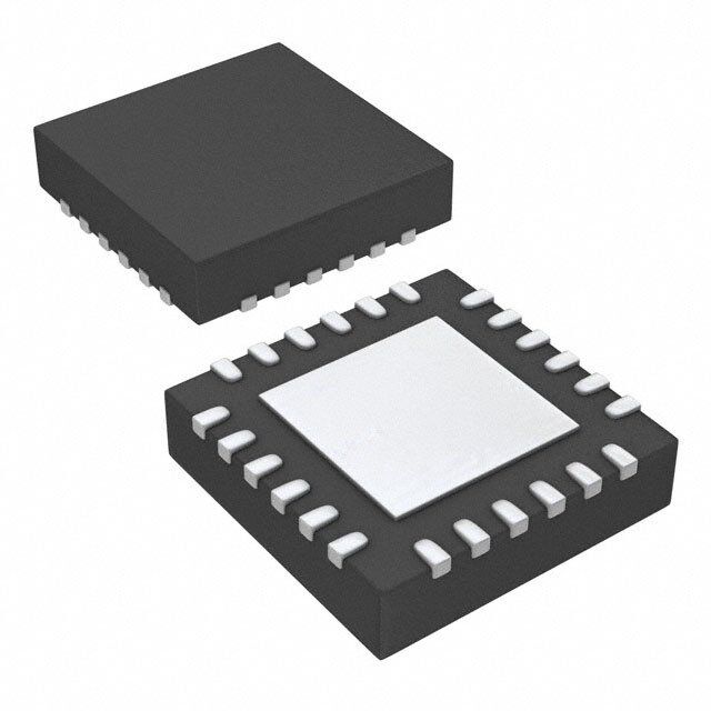
TLC59283 www.ti.com SBVS199B–JUNE2012–REVISEDOCTOBER2012 SWITCHING CHARACTERISTICS AllminimumandmaximumspecificationsareatT =–40°Cto+85°C,V =3Vto5.5V,C =15pF,R =110Ω, A CC L L R =1.5kΩ,andV =5.0V,unlessotherwisenoted.TypicalvaluesareatT =+25°CandV =3.3V. IREF LED A CC TLC59283 PARAMETER TESTCONDITIONS MIN TYP MAX UNIT t SOUT(seeFigure7) 3 10 ns R0 Risetime t OUTn(seeFigure6) 44 ns R1 t SOUT(seeFigure7) 3 10 ns F0 Falltime t OUTn(seeFigure6) 44 ns F1 t SCLK↑toSOUT↑↓ 11 20 ns D0 t LAT↑orBLANK↑↓toOUT0onoroff,T =+25°C 60 100 ns D1 Propagationdelaytime A GroupedOUTnonorofftonextgrouponoroff, t 2 ns D2 T =+25°C A t Outputon-timeerror(1) Outputonorofflatchdata=all'1',50-nsBLANKGND –45 45 ns ON_ERR levelpulse,V =3.3V,T =+25°C CC A (1) Outputon-timeerror(t )iscalculatedbytheformula:t (ns)=t –BLANKlowlevelone-shotpulsewidth(t ). ON_ERR ON_ERR OUT_ON WL2 t indicatestheactualon-timeoftheconstant-currentoutput. OUT_ON PIN CONFIGURATIONS DBQPACKAGE SSOP-24ANDQSOP-24 RGEPACKAGE (TOPVIEW) QFN-24 (TOPVIEW) GND 1 24 VCC CLK N ND CC EF OUT S SI G V R S I SIN 2 23 IREF 4 3 2 1 0 9 2 2 2 2 2 1 SCLK 3 22 SOUT LAT 4 21 BLANK LAT 1 18 BLANK OUT0 5 20 OUT15 OUT0 2 17 OUT15 OUT1 6 19 OUT14 OUT1 3 Thermal Pad 16 OUT14 (Bottom Side) OUT2 7 18 OUT13 OUT2 4 15 OUT13 OUT3 8 17 OUT12 OUT3 5 14 OUT12 OUT4 9 16 OUT11 OUT4 6 13 OUT11 OUT5 10 15 OUT10 OUT6 11 14 OUT9 7 8 9 10 11 12 5 6 7 8 9 0 OUT7 12 13 OUT8 T T T T T 1 U U U U U T O O O O O U O NOTE:ThermalpadisnotconnectedtoGNDinternally.ThethermalpadmustbeconnectedtoGNDviatheprintedcircuitboard(PCB) pattern. Copyright©2012,TexasInstrumentsIncorporated SubmitDocumentationFeedback 5 ProductFolderLinks:TLC59283
TLC59283 SBVS199B–JUNE2012–REVISEDOCTOBER2012 www.ti.com PINDESCRIPTIONS PIN NUMBER NAME DBQ RGE I/O DESCRIPTION Alloutputsempty(blank);Schmittbufferinput.WhenBLANKishigh,allconstant-currentoutputs (OUT0toOUT15)areforcedoffandallpre-chargeFETsareturnedon.WhenBLANKislow,all BLANK 21 18 I constant-currentoutputsarecontrolledbythedataintheoutputonoroffdatalatchandallpre- chargeFETsareturnedoff.ThispinisinternallypulleduptoV witha500-kΩ(typ)resistor. CC GND 1 22 — Powerground Constant-currentvaluesetting,theOUT0toOUT15sinkconstant-currentoutputsaresettothe IREF 23 20 I/O desiredvaluesbyconnectinganexternalresistorbetweenIREFandGND. Level-triggeredlatch;Schmittbufferinput.Thedatainthe16-bitshiftregistercontinuetotransfer totheoutputonoroffdatalatchwhileLATishigh.Therefore,ifthedatainthe16-bitshiftregister LAT 4 1 I arechangedwhenLATishigh,thedatainthedatalatcharealsochanged.Thedatainthedata latchareheldwhenLATislow.ThispinisinternallypulleddowntoGNDwitha500-kΩ(typ) resistor. Constant-currentoutput.Eachoutputcanbetiedtogetherwithotherstoincreasetheconstant- OUT0 5 2 O current.Differentvoltagescanbeappliedtoeachoutput. OUT1 6 3 O Constant-currentoutput OUT2 7 4 O Constant-currentoutput OUT3 8 5 O Constant-currentoutput OUT4 9 6 O Constant-currentoutput OUT5 10 7 O Constant-currentoutput OUT6 11 8 O Constant-currentoutput OUT7 12 9 O Constant-currentoutput OUT8 13 10 O Constant-currentoutput OUT9 14 11 O Constant-currentoutput OUT10 15 12 O Constant-currentoutput OUT11 16 13 O Constant-currentoutput OUT12 17 14 O Constant-currentoutput OUT13 18 15 O Constant-currentoutput OUT14 19 16 O Constant-currentoutput OUT15 20 17 O Constant-currentoutput Serialdatashiftclock;Schmittbufferinput. SCLK 3 24 I Alldatainthe16-bitshiftregisterareshiftedtowardtheMSBbya1-bitSCLKsynchronization. Serialdatainputfordriveronoroffcontrol;Schmittbufferinput. WhenSINishigh,theLSBissetto'1'foronlyoneSCLKinputrisingedge.IftwoSCLKrising SIN 2 23 I edgesareinputwhileSINishigh,thenthe16-bitshiftregisterLSBandLSB+1aresetto'1'. WhenSINislow,theLSBissetto'0'attheSCLKinputrisingedge. Serialdataoutput.Thisoutputisconnectedtothe16-bitshiftregisterMSB.SOUTdatachanges SOUT 22 19 O attheSCLKrisingedge. VCC 24 21 — Power-supplyvoltage 6 SubmitDocumentationFeedback Copyright©2012,TexasInstrumentsIncorporated ProductFolderLinks:TLC59283
TLC59283 www.ti.com SBVS199B–JUNE2012–REVISEDOCTOBER2012 FUNCTIONAL BLOCK DIAGRAM VCC VCC SIN LSB MSB 16-Bit Shift Register SCLK (1 Bit x 16 Channels) SOUT 0 ¼ 15 LSB MSB LAT Output On or Off Data Latch (1 Bit x 16 Channels) 0 ¼ 15 BLANK 16-Channel Constant-Current Sink Driver ALLOFF IREF with Grouped Switching Delay VCC-1.4 V Timing (typ) Control GND GND Pre-Charge FETs ¼ OUT0 OUT1 OUT14 OUT15 Copyright©2012,TexasInstrumentsIncorporated SubmitDocumentationFeedback 7 ProductFolderLinks:TLC59283
TLC59283 SBVS199B–JUNE2012–REVISEDOCTOBER2012 www.ti.com PARAMETER MEASUREMENT INFORMATION PIN-EQUIVALENT INPUT AND OUTPUT SCHEMATIC DIAGRAMS VCC VCC INPUT SOUT GND GND Figure1. SINandSCLK Figure4. SOUT VCC VCC LAT OUTn(1) GND GND Figure2. LAT (1) n=0to15. Figure5. OUT0ThroughOUT15 VCC BLANK GND Figure3. BLANK 8 SubmitDocumentationFeedback Copyright©2012,TexasInstrumentsIncorporated ProductFolderLinks:TLC59283
TLC59283 www.ti.com SBVS199B–JUNE2012–REVISEDOCTOBER2012 TEST CIRCUITS VCC R L V CC IREF OUTn V LED RIREF GND CL Figure6. OUTnRiseandFallTimeTestCircuit VCC V SOUT CC GND CL Figure7. SOUTRiseandFallTimeTestCircuit VCC OUT0 VCC ¼ IREF OUTn ¼ RIREF GND OUT15 V VOUTn OUTfix Figure8. OUTnConstant-CurrentTestCircuit Copyright©2012,TexasInstrumentsIncorporated SubmitDocumentationFeedback 9 ProductFolderLinks:TLC59283
TLC59283 SBVS199B–JUNE2012–REVISEDOCTOBER2012 www.ti.com TIMING DIAGRAMS t , t , t , t , t : WH0 WL0 WH1 WH2 WL2 V CC Input(1) 50% GND t t WH WL t , t , t , t : SU0 SU1 H0 H1 V CC SCLK(1) 50% GND t t SU H V CC Data and Control Clock(1) 50% GND (1) Inputpulseriseandfalltimeis1nsto3ns. Figure9. InputTimingDiagram (1) t , t , t , t , t , t , t , t , t : R0 R1 F0 F1 D0 D1 D2 D3 ON_ERR V CC Input(2) 50% GND t t WL2 D V or V OH OUTn 90% Output 50% 10% V or V OL OUTn t OUT_ON t or t R F (1) t iscalculatedbyt –t . ON_ERR OUTON WL2 (2) Inputpulseriseandfalltimeis1nsto3ns. Figure10. OutputTimingDiagram 10 SubmitDocumentationFeedback Copyright©2012,TexasInstrumentsIncorporated ProductFolderLinks:TLC59283
TLC59283 www.ti.com SBVS199B–JUNE2012–REVISEDOCTOBER2012 SIN DATA DATA DATA DATA DATA DATA DATA DATA DATA DATA DATA DATA DATA DATA DATA DATA 0A 15B 14B 13B 12B 11B 3B 2B 1B 0B 15C 14C 13C 12C 11C 10C t tSU0 H0 t tH1 WH0 t SU1 SCLK 1 2 3 4 5 13 14 15 16 1 2 3 4 5 6 t t WH1 WL0 LAT Shift Register DATA DATA DATA DATA DATA DATA DATA DATA DATA DATA DATA DATA DATA DATA LSB Data (Internal) 0A 15B 14B 13B 12B 3B 2B 1B 0B 15C 14C 13C 12C 11C Shift Register DATA DATA DATA DATA DATA DATA DATA DATA DATA DATA DATA DATA DATA DATA LSB+1 Data (Internal) 1A 0A 15B 14B 13B 4B 3B 2B 1B 0B 15C 14C 13C 12C ¼ ¼ ¼ ¼ Shift Register DATA DATA DATA DATA DATA DATA DATA DATA DATA DATA DATA DATA DATA DATA MSB-1 Data (Internal) 14A 13A 12A 11A 10A 2A 1A 15B 14B 13B 12B 11B 10B 9B Shift Register DATA DATA DATA DATA DATA DATA DATA DATA DATA DATA DATA DATA DATA DATA MSB Data (Internal) 15A 14A 13A 12A 11A 3A 2A 1A 15B 14B 13B 12B 11B 10B Output On or Off Control Previous On or Off Control Data Latest On or OffControlData Data Latch (Internal)(1) SOUT DATA DATA DATA DATA DATA DATA DATA DATA DATA DATA DATA DATA DATA 15A 14A 13A 12A 2A 1A 0A 15B 14B 13B 12B 11B 10B tD0 tR0/tF0 tWH2 BLANK t WL2 tD1 tD1 OFF OFF OUT0 ON ON t OUTON t t OFF OFF D2 D2 OUT1, 15 ON ON t F1 ¼ ¼ ¼ ¼ tR1 OFF OFF OUT7, 9 ON ON tD2 tD2 OFF OFF OUT8 ON ON ON ON ON Pre-Charge FET OFF OFF (1) Outputonoroffdata=FFFFh. (2) t =t –t . ON_ERR OUTON WL2 Figure11. DataWriteandOutputOnorOffTimingDiagram Copyright©2012,TexasInstrumentsIncorporated SubmitDocumentationFeedback 11 ProductFolderLinks:TLC59283
TLC59283 SBVS199B–JUNE2012–REVISEDOCTOBER2012 www.ti.com TYPICAL CHARACTERISTICS AtT =+25°CandV =3.3V,unlessotherwisenoted. A CC REFERENCERESISTOR OUTPUTCURRENTvs vsOUTPUTCURRENT OUTPUTVOLTAGE(VCC=3.3V) 100 50 45 VCC = 3.3 V IO = 35 mA IO = 10 mA VOUTn = 0.8 V IO = 30 mA IO = 5 mA Wsistor (k) 26.510.6 ent (mA) 334050 TA = +25(cid:176)C IO = 20 mA IO = 2 mA Re 10 urr 25 eference 5.29 3.53 2.65 Output C 1250 R 2.12 1.76 10 1.51 1.32 5 1.18 1 0 0 10 20 30 40 50 0 0.5 1 1.5 2 2.5 3 Output Current (mA) Output Voltage (V) G020 G000 Figure12. Figure13. OUTPUTCURRENTvs OUTPUTCURRENTvsOUTPUTVOLTAGE OUTPUTVOLTAGE(VCC=5.0V) (VCC=3.3V,Magnified) 55 39 50 VCC = 5.0 V, VOUTn = 0.8 V, TA = +25(cid:176)C VCC = 3.3 V IO = 45 mA 38 VOUTn = 0.8 V A) 4405 IO = 40 mA A) 37 IO = 35 mA put Current (m 22330505 IIIOOO === 332500 mmmAAA put Current (m 333456 ut ut O 1105 IO = 10 mA O 33 TA = −40(cid:176)C 5 IIOO == 52 mmAA 32 TTAA == ++2855(cid:176)(cid:176)CC 0 31 0 0.5 1 1.5 2 2.5 3 0 0.5 1 1.5 Output Voltage (V) Output Voltage (V) G001 G004 Figure14. Figure15. OUTPUTCURRENTvsOUTPUTVOLTAGE (VCC=5.0V,Magnified) ΔI vsAMBIENTTEMPERATURE OLC 39 3 VCC = 5.0 V VOUTn = 0.8 V 38 VOUTn = 0.8 V 2 IO = 20 mA IO = 35 mA A) 37 m 1 nt ( 36 %) Curre 35 (OLC 0 utput 34 DI −1 O 33 32 TTAA == −+4205(cid:176)(cid:176)CC −2 VCC = 3.3 V TA = +85(cid:176)C VCC = 5.0 V 31 −3 0 0.5 1 1.5 −40 −20 0 20 40 60 80 100 Output Voltage (V) G005 Ambient Temperature ((cid:176)C) G006 Figure16. Figure17. 12 SubmitDocumentationFeedback Copyright©2012,TexasInstrumentsIncorporated ProductFolderLinks:TLC59283
TLC59283 www.ti.com SBVS199B–JUNE2012–REVISEDOCTOBER2012 TYPICAL CHARACTERISTICS (continued) AtT =+25°CandV =3.3V,unlessotherwisenoted. A CC SUPPLYCURRENTvsOUTPUTCURRENT SUPPLYCURRENTvsAMBIENTTEMPERATURE 12 12 VCC = 5.0 V VCC = 3.3 V 11 VCC = 3.3 V 11 VCC = 5.0 V 10 10 9 A) A) 9 I(mCC 78 I (mCC 8 6 SIN = 17.5 MHz 7 SIN = 17.5 MHz SCLK = 35 MHz SCLK = 35 MHz 5 All Outputs On 6 All Outputs On TA= +25°C IO = 35 mA 4 5 0 10 20 30 40 50 −40 −20 0 20 40 60 80 100 Output Current (mA) G018 Ambient Temperature ((cid:176)C) G008 Figure18. Figure19. CONSTANT-CURRENTOUTPUT VOLTAGEWAVEFORM CH1-BLANK Channel 1 (50 ns) (5 V/div) Channel 2 CH2-OUT0 (2 V/div) (BLANK = 50 ns) Channel 3 (2 V/div) IO= 35 mA CH3-OUT1 T = +25°C (BLANK = 50 ns) A R = 110W L Channel 4 CL= 15 pF CH4-OUT2 (2 V/div) VCC = 5 V (BLANK = 50 ns) V = 5 V LED Time (20 ns/div) G021 Figure20. Copyright©2012,TexasInstrumentsIncorporated SubmitDocumentationFeedback 13 ProductFolderLinks:TLC59283
TLC59283 SBVS199B–JUNE2012–REVISEDOCTOBER2012 www.ti.com DETAILED DESCRIPTION CONSTANT SINK CURRENT VALUE SETTING The constant-current values are determined by an external resistor (R ) placed between IREF and GND. The IREF resistor(R )valueiscalculatedbyEquation1. IREF R (kW) = VIREF(V) ´43.8 IREF I (mA) OLC Where: V =theinternalreferencevoltageontheIREFpin(typically1.208V) (1) IREF I must be set in the range of 2 mA to 35 mA when V is less than 3.6 V. Also, when V is equal to 3.6 V or OLC CC CC greater, I must be set in the range of 2 mA to 45 mA. The constant sink current characteristic for the external OLC resistor value is illustrated in Figure 12. Table 1 describes the constant-current output versus external resistor value. Table1.Constant-CurrentOutputversusExternalResistorValue I (mA) R (kΩ,Typical) OLC IREF 45(V >3.6Vonly) 1.18 CC 40(V >3.6Vonly) 1.32 CC 35 1.51 30 1.76 25 2.12 20 2.65 15 3.53 10 5.29 5 10.6 2 26.5 CONSTANT-CURRENT DRIVER ON OR OFF CONTROL When BLANK is low, the corresponding output is turned on if the data in the on or off control data latch are '1' and remains off if the data are '0'. When BLANK is high, all outputs are forced off. This control is shown in Table2. Table2.OutputOnorOffControlDataTruthTable CONSTANT-CURRENTOUTPUT OUTPUTONOROFFDATA STATUS 0 Off 1 On When the device is initially powered on, the data in the 16-bit shift register and output on or off data latch are not set to default values. Therefore, the output on or off data must be written to the data latch before turning the constant-current output on. BLANK should be high when powered on because the constant-current may be turnedonasaresultofrandomdataintheoutputonoroffdatalatch. 14 SubmitDocumentationFeedback Copyright©2012,TexasInstrumentsIncorporated ProductFolderLinks:TLC59283
TLC59283 www.ti.com SBVS199B–JUNE2012–REVISEDOCTOBER2012 REGISTER CONFIGURATION The TLC59283 has a 16-bit shift register and an output on or off data latch. Both the shift register and data latch are 16 bits long and are used to turn the constant-current outputs on and off. Figure 21 shows the shift register and data latch configuration. The data at the SIN pin are shifted into the 16-bit shift register LSB at the rising edgeoftheSCLKpin;SOUTdatachangeattheSCLKrisingedge. 16-Bit Shift Register (1 Bit´16 Channels) MSB LSB 15 14 13 12 11 4 3 2 1 0 On or Off On or Off On or Off On or Off ¼ On or Off On or Off On or Off On or Off SIN SOUT Data for Data for Data for Data for Data for Data for Data for Data for OUT15 OUT14 OUT13 OUT12 OUT3 OUT2 OUT1 OUT0 SCLK ¼ MSB LSB 15 14 13 12 11 4 3 2 1 0 On or Off On or Off On or Off On or Off ¼ On or Off On or Off On or Off On or Off Data for Data for Data for Data for Data for Data for Data for Data for LAT OUT15 OUT14 OUT13 OUT12 OUT3 OUT2 OUT1 OUT0 Output On or Off Data Latch (1 Bit´16 Channels) 16 Bits To Constant-Current Driver Control Block Figure21. 16-BitShiftRegisterandOutputOnorOffDataLatchConfiguration The output on or off data in the 16-bit shift register continue to transfer to the output on or off data latch while LAT is high. Therefore, if the data in the 16-bit shift register are changed when LAT is high, the data in the data latcharealsochanged.ThedatainthedatalatchareheldwhenLATislow.Whenthedeviceinitiallypowerson, the data in the output on or off shift register and latch are not set to default values; on or off control data must be written to the on or off control data latch before turning the constant-current output on. All constant-current outputs are forced off when BLANK is high. The OUTn on or off outputs are controlled by the data in the output on or off data latch. The writing data truth table and timing diagram are shown in Table 3 and Figure 22, respectively. Table3.TruthTableinOperation SCLK LAT BLANK SIN OUT0…OUT7…OUT15 SOUT ↑ High Low Dn Dn…Dn–7…Dn–15 Dn–15 ↑ Low Low Dn+1 Nochange Dn–14 ↑ High Low Dn+2 Dn+2…Dn–5…Dn–13 Dn–13 ↓ — Low Dn+3 Dn+2…Dn–5…Dn–13 Dn–13 ↓ — High Dn+3 Off Dn–13 Copyright©2012,TexasInstrumentsIncorporated SubmitDocumentationFeedback 15 ProductFolderLinks:TLC59283
TLC59283 SBVS199B–JUNE2012–REVISEDOCTOBER2012 www.ti.com 0 1 2 3 4 5 6 7 8 9 10 11 12 13 14 15 SCLK D15 D14 D13 D12 D11 D10 D9 D8 D7 D6 D5 D4 D3 D2 D1 D0 SIN LAT BLANK D0 OFF OUT0 ON OFF OUT1 D1 ON OFF OUT2 D2 ON D3 OFF OUT3 ON ¼ ¼ ¼ ¼ OFF OUT15 D15 ON SOUT Don’t Care D15 Figure22. OperationTimingDiagram NOISE REDUCTION Largesurgecurrentsmayflowthroughthedeviceandboardifall16outputsturnonoroffsimultaneously.These large current surges can induce detrimental noise and electromagnetic interference (EMI) into other circuits. The TLC59283 independently turns on or off the outputs for each group with a 1-ns (typ) delay time; see Figure 11. The 16 outputs are grouped into nine groups of either one or two outputs: group 1 (OUT0), group 2 (OUT1 and OUT15), group 3 (OUT2 and OUT14), group 4 (OUT3 and OUT13), group 5 (OUT4 and OUT12), group 6 (OUT5 and OUT11), group 7 (OUT6 and OUT10), group 8 (OUT7 and OUT9), and group 9 (OUT9). Both turn-on and turn-off times are delayed when BLANK transitions from low to high or high to low. Also when output-on and -off data are changed at the LAT rising edge while BLANK is low, both turn-on and turn-off times are delayed. However, the state of each output is controlled by the data in the output on or off data latch and the BLANK level. 16 SubmitDocumentationFeedback Copyright©2012,TexasInstrumentsIncorporated ProductFolderLinks:TLC59283
TLC59283 www.ti.com SBVS199B–JUNE2012–REVISEDOCTOBER2012 InternalPre-ChargeFET The internal pre-charge FET prevents ghosting of multiplexed LED modules. One cause of this phenomenon is the parasitic capacitance charging current of the constant-current outputs (OUTn) and PCB wiring connected to OUTnthroughtheLED.OneofthemechanismsisshowninFigure23. In Figure 23, the constant-current driver turns LED0-0 on at (1) and off at (2). After LED0-0 is turned off, the OUT0 voltage is pulled up to V by LED0-0. This OUT0 node has some parasitic capacitance (such as the CHG constant-current driver output capacitance and the board layout capacitance shown as C0-2). After LED0-0 turns off, SWPMOS0 is turned off, SWNMOS0 is turned on for COM0, and COM0 is pulled down to GND. Because there is a parasitic capacitance between COM0 and OUT0, the OUT0 voltage is also pulled down to GND. Afterwards, SWPMOS1 is turned on for the next common line (COM1). When SWPMOS1 turns on, the OUT0 voltage is pulled up from the ground voltage to V – V . The charge current (I ) flows to the parasitic LED F CHRG capacitor(C0)throughLED1-0,causingtheLEDtobrieflyturnonandcreatingaghostingeffectofLED1-0. VLED COM0 is VLED level. (LED Power-Supply) SW ON PMOS0 OFF SW COM0 is GND level. PMOS1 LED1-1 LED1-2 COM1 NMOSSW0 OOFNF COM1 is VLED level. ¼ SW ON elector NMOSSW1 LED1-0 Parasitic Capacitor PMOSSW1 OOFNF COM1 is GND level. e S VLED C0 C1 C2 NMOS1 OFF n Li High Drive SPWMOS0 ICHRG BLANK Low D COM0 ON E OUT0 L OFF VLED NMOSSW0 LED0-0 LED0-1 LED0-2 ¼ VoOltUaTge0 VCHG VLED-V OUT0 OUT1 OUT2 F GND Ordinal LED0-0 20 mA LED Driver OUT0 OUT1 OUT2 ¼ Current 0 mA ON ON ON LED1-0 20 mA Constant-Current Current 0 mA Output (1) (2) (3) (4) Ghost phenomenon is observed OUT0 voltage is pulled down to GND side whenCOM1 goes up to VLED. by the coupling with LED lamp capacitor between COM0 and OUT0. Figure23. LEDGhost-LightingPhenomenonMechanism Copyright©2012,TexasInstrumentsIncorporated SubmitDocumentationFeedback 17 ProductFolderLinks:TLC59283
TLC59283 SBVS199B–JUNE2012–REVISEDOCTOBER2012 www.ti.com The TLC59283 has an internal pre-charge FET to prevent ghosting, as shown in Figure 24. When a small delay after PWM control for a single common line completes, the FET pulls OUTn up to V . The charge current does CC not flow to C0 through LED1-0 when SWMOS1 is turned on and the ghosting is eliminated at (3). However, depending on the LED anode voltage, the number of LEDs in series, the LED forward voltage, and the TLC59283V supplyvoltage,theremaynotbeagreatenoughghost-cancelingeffect. CC VLED (LED Power-Supply) SW PMOS1 LED1-1 LED1-2 SW ON COM0 is VLED level. COM1 PMOS0 OFF ¼ COM0 is GND level. ne Selector NMOSSW1VLED LED1-0 C0 C1 C2Parasitic Capacitor NPMMOOSSSSWW01 OOOOFFNNFF COM1 is VLED level. Drive Li SPWMOS0 Disappearing ICHRG NMOSSW1 OOFNF COM1 is GND level. D COM0 LE BLANK High Low SW LED0-0 LED0-1 LED0-2 ON NMOS0 OUT0 ¼ OFF OUT0 OUT1 OUT2 PCHGON ON Signal OFF Pre-Charge FET VCC VLED VCC-1.4 V (typ) VoOltUaTge0 VCHG Timing PCHGON VLED-VF BLANK Control LED0-0 20 mA GND OUT0 OUT0 OUT0 ¼ Current 0 mA ON ON ON LED1-0 20 mA Constant-Current Current 0 mA Output TLC59283 (1) (2) (3) (4) LED Driver Ghost phenomenon not seen Figure24. LEDGhost-LightingMechanismbyPre-ChargeFET 18 SubmitDocumentationFeedback Copyright©2012,TexasInstrumentsIncorporated ProductFolderLinks:TLC59283
TLC59283 www.ti.com SBVS199B–JUNE2012–REVISEDOCTOBER2012 HISTORY TABLE NOTE:Pagenumbersforpreviousrevisionsmaydifferfrompagenumbersinthecurrentversion. ChangesfromRevisionA(June2012)toRevisionB Page • ChangedHBMESDratingmaximumspecificationintheAbsoluteMaximumRatingstable .............................................. 2 • ChangedI typicalandmaximumspecificationsinElectricalCharacteristicstable.......................................................... 4 CC2 • ChangedI typicalspecificationinElectricalCharacteristicstable ................................................................................... 4 CC3 Copyright©2012,TexasInstrumentsIncorporated SubmitDocumentationFeedback 19 ProductFolderLinks:TLC59283
PACKAGE OPTION ADDENDUM www.ti.com 6-Feb-2020 PACKAGING INFORMATION Orderable Device Status Package Type Package Pins Package Eco Plan Lead/Ball Finish MSL Peak Temp Op Temp (°C) Device Marking Samples (1) Drawing Qty (2) (6) (3) (4/5) TLC59283DBQ ACTIVE SSOP DBQ 24 50 Green (RoHS NIPDAU Level-2-260C-1 YEAR -40 to 85 TLC59283 & no Sb/Br) TLC59283DBQR ACTIVE SSOP DBQ 24 2500 Green (RoHS NIPDAU Level-2-260C-1 YEAR -40 to 85 TLC59283 & no Sb/Br) TLC59283RGER ACTIVE VQFN RGE 24 3000 Green (RoHS NIPDAU Level-2-260C-1 YEAR -40 to 85 TLC & no Sb/Br) 59283 TLC59283RGET ACTIVE VQFN RGE 24 250 Green (RoHS NIPDAU Level-2-260C-1 YEAR -40 to 85 TLC & no Sb/Br) 59283 (1) The marketing status values are defined as follows: ACTIVE: Product device recommended for new designs. LIFEBUY: TI has announced that the device will be discontinued, and a lifetime-buy period is in effect. NRND: Not recommended for new designs. Device is in production to support existing customers, but TI does not recommend using this part in a new design. PREVIEW: Device has been announced but is not in production. Samples may or may not be available. OBSOLETE: TI has discontinued the production of the device. (2) RoHS: TI defines "RoHS" to mean semiconductor products that are compliant with the current EU RoHS requirements for all 10 RoHS substances, including the requirement that RoHS substance do not exceed 0.1% by weight in homogeneous materials. Where designed to be soldered at high temperatures, "RoHS" products are suitable for use in specified lead-free processes. TI may reference these types of products as "Pb-Free". RoHS Exempt: TI defines "RoHS Exempt" to mean products that contain lead but are compliant with EU RoHS pursuant to a specific EU RoHS exemption. Green: TI defines "Green" to mean the content of Chlorine (Cl) and Bromine (Br) based flame retardants meet JS709B low halogen requirements of <=1000ppm threshold. Antimony trioxide based flame retardants must also meet the <=1000ppm threshold requirement. (3) MSL, Peak Temp. - The Moisture Sensitivity Level rating according to the JEDEC industry standard classifications, and peak solder temperature. (4) There may be additional marking, which relates to the logo, the lot trace code information, or the environmental category on the device. (5) Multiple Device Markings will be inside parentheses. Only one Device Marking contained in parentheses and separated by a "~" will appear on a device. If a line is indented then it is a continuation of the previous line and the two combined represent the entire Device Marking for that device. (6) Lead/Ball Finish - Orderable Devices may have multiple material finish options. Finish options are separated by a vertical ruled line. Lead/Ball Finish values may wrap to two lines if the finish value exceeds the maximum column width. Important Information and Disclaimer:The information provided on this page represents TI's knowledge and belief as of the date that it is provided. TI bases its knowledge and belief on information provided by third parties, and makes no representation or warranty as to the accuracy of such information. Efforts are underway to better integrate information from third parties. TI has taken and Addendum-Page 1
PACKAGE OPTION ADDENDUM www.ti.com 6-Feb-2020 continues to take reasonable steps to provide representative and accurate information but may not have conducted destructive testing or chemical analysis on incoming materials and chemicals. TI and TI suppliers consider certain information to be proprietary, and thus CAS numbers and other limited information may not be available for release. In no event shall TI's liability arising out of such information exceed the total purchase price of the TI part(s) at issue in this document sold by TI to Customer on an annual basis. Addendum-Page 2
PACKAGE MATERIALS INFORMATION www.ti.com 8-May-2015 TAPE AND REEL INFORMATION *Alldimensionsarenominal Device Package Package Pins SPQ Reel Reel A0 B0 K0 P1 W Pin1 Type Drawing Diameter Width (mm) (mm) (mm) (mm) (mm) Quadrant (mm) W1(mm) TLC59283DBQR SSOP DBQ 24 2500 330.0 16.4 6.5 9.0 2.1 8.0 16.0 Q1 TLC59283RGER VQFN RGE 24 3000 330.0 12.4 4.25 4.25 1.15 8.0 12.0 Q2 TLC59283RGET VQFN RGE 24 250 180.0 12.4 4.25 4.25 1.15 8.0 12.0 Q2 PackMaterials-Page1
PACKAGE MATERIALS INFORMATION www.ti.com 8-May-2015 *Alldimensionsarenominal Device PackageType PackageDrawing Pins SPQ Length(mm) Width(mm) Height(mm) TLC59283DBQR SSOP DBQ 24 2500 367.0 367.0 38.0 TLC59283RGER VQFN RGE 24 3000 367.0 367.0 35.0 TLC59283RGET VQFN RGE 24 250 210.0 185.0 35.0 PackMaterials-Page2
None
None
GENERIC PACKAGE VIEW RGE 24 VQFN - 1 mm max height PLASTIC QUAD FLATPACK - NO LEAD Images above are just a representation of the package family, actual package may vary. Refer to the product data sheet for package details. 4204104/H
PACKAGE OUTLINE RGE0024C VQFN - 1 mm max height PLASTIC QUAD FLATPACK- NO LEAD A 4.1 B 3.9 4.1 PIN 1 INDEX AREA 3.9 1 MAX C SEATING PLANE 0.05 0.00 2X 2.5 0.08 C 2.1±0.1 (0.2) TYP 7 12 20X 0.5 6 13 2X 25 SYMM 2.5 1 18 0.30 PIN 1 ID 24X 0.18 (OPTIONAL) 24 19 0.1 C A B SYMM 0.50 0.05 C 24X 0.30 4224376 A 072018 NOTES: 1. All linear dimensions are in millimeters. Any dimensions in parenthesis are for reference only. Dimensioning and tolerancing per ASME Y14.5M. 2. This drawing is subject to change without notice. 3. The package thermal pad must be soldered to the printed circuit board for thermal and mechanical performance. www.ti.com
EXAMPLE BOARD LAYOUT RGE0024C VQFN - 1 mm max height PLASTIC QUAD FLATPACK- NO LEAD (3.8) ( 2.1) 24 19 24X (0.6) 24X (0.24) 1 18 20X (0.5) 25 SYMM (3.8) 2X (0.8) (Ø0.2) VIA TYP 6 13 (R0.05) 7 12 2X(0.8) SYMM LAND PATTERN EXAMPLE SCALE: 20X 0.07 MAX 0.07 MIN ALL AROUND METAL ALL AROUND SOLDER MASK OPENING SOLDER MASK METAL UNDER OPENING SOLDER MASK NON SOLDER MASK DEFINED SOLDER MASK (PREFERRED) DEFINED SOLDER MASK DETAILS 4224376 A 072018 NOTES: (continued) 4. This package is designed to be soldered to a thermal pad on the board. For more information, see Texas Instruments literature number SLUA271 (www.ti.comlitslua271) . 5. Solder mask tolerances between and around signal pads can vary based on board fabrication site. www.ti.com
EXAMPLE STENCIL DESIGN RGE0024C VQFN - 1 mm max height PLASTIC QUAD FLATPACK- NO LEAD (0.19) 4X ( 0.94) 24 19 24X (0.58) 24X (0.24) 1 18 20X (0.5) SYMM (3.8) (0.57) TYP 6 13 (R0.05) TYP 25 METAL TYP 7 12 (0.57) TYP SYMM SOLDER PASTE EXAMPLE BASED ON 0.125 mm THICK STENCIL EXPOSED PAD 80 PRINTED COVERAGE BY AREA SCALE: 20X 4224376 A 072018 NOTES: (continued) 6. Laser cutting apertures with trapezoidal walls and rounded corners may offer better paste release. IPC-7525 may have alternate design recommendations.. www.ti.com
IMPORTANTNOTICEANDDISCLAIMER TI PROVIDES TECHNICAL AND RELIABILITY DATA (INCLUDING DATASHEETS), DESIGN RESOURCES (INCLUDING REFERENCE DESIGNS), APPLICATION OR OTHER DESIGN ADVICE, WEB TOOLS, SAFETY INFORMATION, AND OTHER RESOURCES “AS IS” AND WITH ALL FAULTS, AND DISCLAIMS ALL WARRANTIES, EXPRESS AND IMPLIED, INCLUDING WITHOUT LIMITATION ANY IMPLIED WARRANTIES OF MERCHANTABILITY, FITNESS FOR A PARTICULAR PURPOSE OR NON-INFRINGEMENT OF THIRD PARTY INTELLECTUAL PROPERTY RIGHTS. These resources are intended for skilled developers designing with TI products. You are solely responsible for (1) selecting the appropriate TI products for your application, (2) designing, validating and testing your application, and (3) ensuring your application meets applicable standards, and any other safety, security, or other requirements. These resources are subject to change without notice. TI grants you permission to use these resources only for development of an application that uses the TI products described in the resource. Other reproduction and display of these resources is prohibited. No license is granted to any other TI intellectual property right or to any third party intellectual property right. TI disclaims responsibility for, and you will fully indemnify TI and its representatives against, any claims, damages, costs, losses, and liabilities arising out of your use of these resources. TI’s products are provided subject to TI’s Terms of Sale (www.ti.com/legal/termsofsale.html) or other applicable terms available either on ti.com or provided in conjunction with such TI products. TI’s provision of these resources does not expand or otherwise alter TI’s applicable warranties or warranty disclaimers for TI products. Mailing Address: Texas Instruments, Post Office Box 655303, Dallas, Texas 75265 Copyright © 2020, Texas Instruments Incorporated