ICGOO在线商城 > 集成电路(IC) > PMIC - LED 驱动器 > TPS61151DRCR

 Datasheet下载
- 型号: TPS61151DRCR
- 制造商: Texas Instruments
- 库位|库存: xxxx|xxxx
- 要求:
| 数量阶梯 | 香港交货 | 国内含税 |
| +xxxx | $xxxx | ¥xxxx |
查看当月历史价格
查看今年历史价格
TPS61151DRCR产品简介:
ICGOO电子元器件商城为您提供TPS61151DRCR由Texas Instruments设计生产,在icgoo商城现货销售,并且可以通过原厂、代理商等渠道进行代购。 TPS61151DRCR价格参考¥6.28-¥14.14。Texas InstrumentsTPS61151DRCR封装/规格:PMIC - LED 驱动器, LED 驱动器 IC 2 输出 DC DC 稳压器 升压 PWM 调光 35mA 10-VSON(3x3)。您可以下载TPS61151DRCR参考资料、Datasheet数据手册功能说明书,资料中有TPS61151DRCR 详细功能的应用电路图电压和使用方法及教程。
TPS61151DRCR 是 Texas Instruments(德州仪器)推出的一款升压型 LED 驱动器,广泛应用于需要高效驱动LED的场景。其主要应用场景包括:

1. 便携式设备背光:如智能手机、平板电脑、GPS设备等的LCD屏幕背光驱动,适用于白光LED阵列。

2. 手持设备照明:例如手电筒、便携式灯具等,利用其高效率和小尺寸优势。

3. 工业与汽车仪表显示:用于仪表盘、控制面板等需要稳定LED亮度的显示系统。

4. 消费类电子产品:如数码相机、电子书阅读器等设备中的LED照明驱动。

该器件采用升压拓扑结构,可将较低输入电压升至适合驱动多个LED的电压水平,支持模拟和PWM调光功能,具备过温保护和短路保护等安全机制,适合对效率、稳定性和空间有要求的应用场合。
| 参数 | 数值 |
| 产品目录 | 集成电路 (IC)光电子产品 |
| 描述 | IC LED DRVR WT/OLED BCKLT 10-SONLED照明驱动器 Dual 700mA Switch 1.2MHz Boost Cnvrtr |
| 产品分类 | |
| 品牌 | Texas Instruments |
| 产品手册 | |
| 产品图片 |
|
| rohs | 符合RoHS无铅 / 符合限制有害物质指令(RoHS)规范要求 |
| 产品系列 | LED照明电子器件,LED照明驱动器,Texas Instruments TPS61151DRCR- |
| 数据手册 | |
| 产品型号 | TPS61151DRCR |
| 产品目录页面 | |
| 产品种类 | LED照明驱动器 |
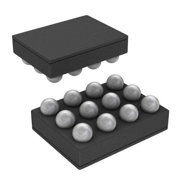
| 供应商器件封装 | 10-SON(3x3) |
| 其它名称 | 296-21162-1 |
| 内部驱动器 | 是 |
| 包装 | 剪切带 (CT) |
| 单位重量 | 26.100 mg |
| 商标 | Texas Instruments |
| 安装类型 | 表面贴装 |
| 安装风格 | SMD/SMT |
| 封装 | Reel |
| 封装/外壳 | 10-VFDFN 裸露焊盘 |
| 封装/箱体 | VSON-10 |
| 工作温度 | -40°C ~ 85°C |
| 工作频率 | 1.2 MHz |
| 工厂包装数量 | 3000 |
| 恒压 | - |
| 恒流 | - |
| 拓扑 | PWM,升压(升压) |
| 拓扑结构 | Boost |
| 最大工作温度 | + 85 C |
| 最大电源电流 | 2 mA |
| 最小工作温度 | - 40 C |
| 标准包装 | 1 |
| 电压-电源 | 2.5 V ~ 6 V |
| 电压-输出 | 27V |
| 类型 | Inductive |
| 类型-初级 | 背光 |
| 类型-次级 | 白色 LED |
| 系列 | TPS61151 |
| 输入电压 | 2.5 V to 6 V |
| 输出数 | 2 |
| 输出电流 | 700 mA |
| 输出端数量 | 2 Output |
| 输出类型 | Current Mode |
| 配用 | /product-detail/zh/TPS61150EVM-150/296-19745-ND/1087460 |
| 频率 | 1MHz ~ 1.5MHz |


- 商务部:美国ITC正式对集成电路等产品启动337调查
- 曝三星4nm工艺存在良率问题 高通将骁龙8 Gen1或转产台积电
- 太阳诱电将投资9.5亿元在常州建新厂生产MLCC 预计2023年完工
- 英特尔发布欧洲新工厂建设计划 深化IDM 2.0 战略
- 台积电先进制程称霸业界 有大客户加持明年业绩稳了
- 达到5530亿美元!SIA预计今年全球半导体销售额将创下新高
- 英特尔拟将自动驾驶子公司Mobileye上市 估值或超500亿美元
- 三星加码芯片和SET,合并消费电子和移动部门,撤换高东真等 CEO
- 三星电子宣布重大人事变动 还合并消费电子和移动部门
- 海关总署:前11个月进口集成电路产品价值2.52万亿元 增长14.8%


PDF Datasheet 数据手册内容提取
Product Sample & Technical Tools & Support & Folder Buy Documents Software Community TPS61150,TPS61151 SLVS625E–FEBRUARY2006–REVISEDNOVEMBER2015 TPS6115x Dual-Output Boost WLED Driver Using Single Inductor 1 Features 3 Description • 2.5-Vto6-VInputVoltageRange The TPS6115x is a high-frequency boost converter 1 with two regulated current outputs for driving WLEDs. • TwoOutputsEachupto27V Each current output can be individually programmed • 0.7-AIntegratedSwitch through external resistors. There is a dedicated • Built-InPowerDiode selection pin for each output so the two outputs can be turned on separately or simultaneously. The • 1.2-MHzFixedPWMFrequency output current can be reduced by a pulse width • IndividuallyProgrammableOutputCurrent modulation (PWM) signal on SEL pins or an analog • Input-to-OutputIsolation voltage on the ISET pins, resulting in PWM dimming of the WLEDs. The boost regulator runs at a 1.2-MHz • Built-InSoftStart fixed switching frequency to reduce output ripple and • OvervoltageProtection avoid audible noises associated with pulse frequency • Upto83%Efficiency modulation(PFM)control. • Upto30-kHzPWMDimmingFrequency The two current outputs are ideal for driving WLED backlights for the sub and main displays in clamshell 2 Applications phones. The two outputs can also be used for driving display and keypad backlights. When used together, • Sub-andMain-DisplayBacklightinClamshell the two outputs can drive up to 14 WLEDs for one Phones largedisplay. • DisplayandKeypadBacklight In addition to the small inductor, small capacitor, and • Upto14-WLEDDriver 3-mm × 3-mm VSON package, the built-in MOSFET and diode eliminate the need for any external power devices. Overall, the device provides an extremely compact solution with high efficiency and plenty of flexibility. DeviceInformation(1) PARTNUMBER PACKAGE BODYSIZE(NOM) TPS61150 VSON(10) 3.00mm×3.00mm TPS61151 (1) For all available packages, see the orderable addendum at theendofthedatasheet. TypicalApplication 2.5 V to 6 V Input L1 10μH C1 1μF VIN SW IOUT C2 GND 1μF SEL1 SEL2 IFB1 IFB2 ISET1 ISET2 R1 R2 1 An IMPORTANT NOTICE at the end of this data sheet addresses availability, warranty, changes, use in safety-critical applications, intellectualpropertymattersandotherimportantdisclaimers.PRODUCTIONDATA.
TPS61150,TPS61151 SLVS625E–FEBRUARY2006–REVISEDNOVEMBER2015 www.ti.com Table of Contents 1 Features.................................................................. 1 8.4 DeviceFunctionalModes..........................................9 2 Applications........................................................... 1 9 ApplicationandImplementation........................ 10 3 Description............................................................. 1 9.1 ApplicationInformation............................................10 4 RevisionHistory..................................................... 2 9.2 TypicalApplication .................................................10 9.3 AdditionalApplicationCircuits.................................16 5 DeviceComparisonTables................................... 3 10 PowerSupplyRecommendations..................... 17 6 PinConfigurationandFunctions......................... 3 11 Layout................................................................... 17 7 Specifications......................................................... 4 11.1 LayoutGuidelines.................................................17 7.1 AbsoluteMaximumRatings......................................4 11.2 LayoutExample....................................................17 7.2 ESDRatings..............................................................4 12 DeviceandDocumentationSupport................. 18 7.3 RecommendedOperatingConditions.......................4 7.4 ThermalInformation..................................................4 12.1 DeviceSupport......................................................18 7.5 ElectricalCharacteristics...........................................5 12.2 RelatedLinks........................................................18 7.6 TypicalCharacteristics..............................................6 12.3 CommunityResources..........................................18 12.4 Trademarks...........................................................18 8 DetailedDescription.............................................. 8 12.5 ElectrostaticDischargeCaution............................18 8.1 Overview...................................................................8 12.6 Glossary................................................................18 8.2 FunctionalBlockDiagram.........................................8 13 Mechanical,Packaging,andOrderable 8.3 FeatureDescription...................................................8 Information........................................................... 18 4 Revision History NOTE:Pagenumbersforpreviousrevisionsmaydifferfrompagenumbersinthecurrentversion. ChangesfromRevisionD(July2009)toRevisionE Page • Changed"QFN"packageto"VSON"throughoutdocument.................................................................................................. 1 • AddedDeviceInformationandPinConfigurationandFunctionssections,ESDRatingsandThermalInformation tables,FeatureDescription,DeviceFunctionalModes,ApplicationandImplementation,PowerSupply Recommendations,Layout,DeviceandDocumentationSupport,andMechanical,Packaging,andOrderable Informationsections................................................................................................................................................................ 1 • DeletedobsoleteDissipationRatingstable ........................................................................................................................... 5 ChangesfromRevisionC(November2008)toRevisionD Page • DeletedLeadtemperaturespecificationfromAbsoluteMaximumRatingstable................................................................... 4 • CorrectedFETerrorinFigure9........................................................................................................................................... 11 2 SubmitDocumentationFeedback Copyright©2006–2015,TexasInstrumentsIncorporated ProductFolderLinks:TPS61150 TPS61151
TPS61150,TPS61151 www.ti.com SLVS625E–FEBRUARY2006–REVISEDNOVEMBER2015 5 Device Comparison Tables Table1.OVPOptions T PACKAGE(1) OVP PACKAGE A (TYPICAL) MARKING –40to+85°C TPS61150DRCR 28V BCQ –40to+85°C TPS61151DRCR 22V BRH –40to+85°C TPS61150DRCT 28V BCQ –40to+85°C TPS61151DRCT 22V BRH (1) Forthemostcurrentpackageandorderinginformation,seethePackageOptionAddendumattheendofthisdocument,orseetheTI websiteatwww.ti.com. Table2.TPS6115xModeSelection SEL1 SEL2 IFB1 IFB2 H L Enable Disable L H Disable Enable H H Enable Enable L L Deviceshutdown 6 Pin Configuration and Functions DRCPackage 10-PinVSONWithExposedThermalPad TopView IFB1 1 10 IFB2 ISET1 2 9 ISET2 Exposed SEL1 3 Thermal 8 GND Pad SEL2 4 7 IOUT VIN 5 6 SW PinFunctions PIN I/O DESCRIPTION NUMBER NAME ThereturnpathfortheI regulation.Currentregulatorisconnectedtothispin,and 1,10 IFB1,IFB2 I OUT itcanbedisabledtoopenthecurrentpath. Outputcurrentprogrammingpins.Theresistorconnectedtothepinprogramsits 2,9 ISET1,ISET2 I correspondingoutputcurrent. 3,4 SEL1,SEL2 I Modeselectionpins.SeeTable2fordetails. Theinputpintothedevice.Itprovidesthecurrenttotheboostpowerstageandalso 5 VIN I powersthedevicecircuit.WhenV isbelowtheundervoltagelockoutthreshold,the IN deviceturnsoffanddisablesoutputs,thusdisconnectingtheWLEDsfromtheinput. 6 SW I Thisistheswitchingnodeofthedevice. Theoutputoftheconstantcurrentsupply.Itisdirectlyconnectedtotheboost 7 IOUT O converteroutput. Thegroundofthedevice.Connecttheinputandoutputcapacitorsveryclosetothis 8 GND O pin. Thethermalpadshouldbesolderedtotheanalogground.Ifpossible,usethermalvia — ThermalPad — toconnecttogroundplaneforidealpowerdissipation. Copyright©2006–2015,TexasInstrumentsIncorporated SubmitDocumentationFeedback 3 ProductFolderLinks:TPS61150 TPS61151
TPS61150,TPS61151 SLVS625E–FEBRUARY2006–REVISEDNOVEMBER2015 www.ti.com 7 Specifications 7.1 Absolute Maximum Ratings overoperatingfree-airtemperaturerange(unlessotherwisenoted)(1)(2) MIN MAX UNIT SupplyvoltagesonpinVIN(2) –0.3 V VoltagesonpinsSEL1,SEL2,ISET1andISET2(2) –0.3 V VoltageonpinIOUT,SW,IFB1andIFB2(2) 30 V Operatingjunctiontemperature –40 150 °C Storagetemperature,T –65 150 °C stg (1) StressesbeyondthoselistedunderAbsoluteMaximumRatingsmaycausepermanentdamagetothedevice.Thesearestressratings only,whichdonotimplyfunctionaloperationofthedeviceattheseoranyotherconditionsbeyondthoseindicatedunderRecommended OperatingConditions.Exposuretoabsolute-maximum-ratedconditionsforextendedperiodsmayaffectdevicereliability. (2) Allvoltagevaluesarewithrespecttonetworkgroundpin. 7.2 ESD Ratings VALUE UNIT Electrostatic Human-bodymodel(HBM),perANSI/ESDA/JEDECJS-001(1) ±2000 V V (ESD) discharge Charged-devicemodel(CDM),perJEDECspecificationJESD22-C101(2) ±1500 (1) JEDECdocumentJEP155statesthat500-VHBMallowssafemanufacturingwithastandardESDcontrolprocess. (2) JEDECdocumentJEP157statesthat250-VCDMallowssafemanufacturingwithastandardESDcontrolprocess. 7.3 Recommended Operating Conditions overoperatingfree-airtemperaturerange(unlessotherwisenoted). MIN NOM MAX UNIT V Inputvoltage 2.5 6 V I V Outputvoltage V 27 V O IN L Inductor(1) 10 μH C Inputcapacitor(1) 1 μF IN C Outputcapacitor(1) 1 μF O T Operatingambienttemperature –40 85 °C A T Operatingjunctiontemperature –40 125 °C J (1) SeetheApplicationandImplementationsectionforfurtherinformation. 7.4 Thermal Information TPS6115x THERMALMETRIC(1) DRC(VSON) UNIT 10PINS R Junction-to-ambientthermalresistance 44.3 °C/W θJA R Junction-to-case(top)thermalresistance 56.1 °C/W θJC(top) R Junction-to-boardthermalresistance 19.2 °C/W θJB ψ Junction-to-topcharacterizationparameter 0.7 °C/W JT ψ Junction-to-boardcharacterizationparameter 19.4 °C/W JB R Junction-to-case(bottom)thermalresistance 5.5 °C/W θJC(bot) (1) Formoreinformationabouttraditionalandnewthermalmetrics,seetheSemiconductorandICPackageThermalMetricsapplication report,SPRA953. 4 SubmitDocumentationFeedback Copyright©2006–2015,TexasInstrumentsIncorporated ProductFolderLinks:TPS61150 TPS61151
TPS61150,TPS61151 www.ti.com SLVS625E–FEBRUARY2006–REVISEDNOVEMBER2015 7.5 Electrical Characteristics AtV =3.6V,SELx=V ,R =80kΩ,V =15V,andT =–40°Cto+85°C.TypicalvaluesareatT =25°C(unless I IN SET IO A A otherwisenoted). PARAMETER TESTCONDITIONS MIN TYP MAX UNIT SUPPLYCURRENT V Inputvoltagerange 2.5 6 V I I Operatingquiescentcurrentinto Q DevicePWMswitchingnoload 2 mA V IN I Shutdowncurrent SELx=GND 1.5 μA SD V Undervoltagelockoutthreshold V falling 1.65 1.8 V UVLO IN V Undervoltagelockouthysterisis 70 mV hys ENABLEANDSOFTSTART V SELlogichighvoltage V =2.7Vto6V 1.2 V (selh) IN V SELlogiclowvoltage V =2.7Vto6V 0.4 V (sell) IN R SELpulldownresistor 300 700 kΩ (en) T SELpulsewidthtodisable SELxhightolow 40 ms off K IFBsoftstartcurrentsteps 16 ss T Softstarttimestep Measuredasclockdivider 64 ss Timebetweenfallingandrisingoftwo T Softstartenabletime 40 ms ss_en adjacentSELxpulses CURRENTFEEDBACK V ISETpinvoltage 1.204 1.229 1.254 V (ISET) K Currentmultiplier I /I 820 900 990 (ISET) OUT SET Inreferencetotheaverageoftwooutput K Currentmatching –6% 6% M current V IFBregulationvoltage 300 330 360 mV (IFB) V IFBlowthresholdhysteresis 60 mV (IFB_L) Currentsinksettletimemeasured Tisink fromSELxrisingedge(1) 6 μs I IFBpinleakagecurrent I voltage=25V 1 μA lkg FB POWERSWITCHANDDIODE r N-channelMOSFETon-resistance V =V =3.6V 0.6 0.9 Ω DS(on) IN GS I N-channelleakagecurrent V =25V 1 μA (LN_NFET) DS V Powerdiodeforwardvoltage I =0.7A 0.83 1 V F D OCANDOVP Dualoutput,I =15V,D=76% 0.75 1 1.25 OUT I N-ChannelMOSFETcurrentlimit A LIM Singleoutput,I =15V,D=76% 0.40 0.55 0.7 OUT I Currentsinkmaxoutputcurrent I =330mV 35 mA (IFB_MAX) FB TPS61150 27 28 29 V Overvoltagethreshold V OVP TPS61151 21 22 23 TPS61150 550 V Overvoltagehysteresis mV OVP(hys) TPS61151 440 PWMANDPFMCONTROL ƒ Oscillatorfrequency 1 1.2 1.5 MHz S D Maximumdutycycle V =1V 90% 93% max FB THERMALSHUTDOWN T Thermalshutdownthreshold 160 °C shutdown Thermalshutdownthreshold T 15 °C hys hysteresis (1) ThisspecificationdeterminestheminimumontimerequiredforPWMdimmingfordesirablelinearity.ThemaximumPWMdimming frequencycanbecalculatedfromtheminimumdutycyclerequiredintheapplication. Copyright©2006–2015,TexasInstrumentsIncorporated SubmitDocumentationFeedback 5 ProductFolderLinks:TPS61150 TPS61151
TPS61150,TPS61151 SLVS625E–FEBRUARY2006–REVISEDNOVEMBER2015 www.ti.com 7.6 Typical Characteristics DataforallcharacteristicgraphsweretakenusingtheTypicalApplicationwithinductor=10μH(VLCF4018T-100MR74-2), R1=R2=56kΩ,unlessotherwisenoted. Table3.TableOfGraphs FIGURE Overcurrentlimit V =3V,3.6V,and4V,Singleanddualoutput Figure1,Figure2 IN Kvalueovercurrent V =3.6V,I =2mAto25mA Figure3 IN LOAD PWMdimminglinearity Frequency=20kHzand30kHz Figure4 SingleoutputPWM Figure5 dimmingwaveform MultiplexedPWM Figure6 dimmingwaveform Start-upwaveform Figure7 600 1200 VI= 4.2 V Vin = 3 V 500 1000 VI= 3.6 V mA 400 mA 800 Vin = 3.6 V mit - VI= 3 V mit - Li 300 Li 600 Vin = 4.2 V nt nt e e urr urr C 200 C 400 100 200 0 0 10 20 30 40 50 60 70 80 90 10 20 30 40 50 60 70 80 90 Duty Cycle - % Duty Cycle - % Figure1.OvercurrentLimit(SingleOutput)vsDutyCycle Figure2.OvercurrentLimit(DualOutput)vsDutyCycle 950 25 VI= 3.6 V 930 WLED Voltage = 15 V 910 20 890 A m 870 nt - 15 alue 850 urre V c K D 830 E 10 L W 810 f = 20 kHz 790 5 770 f = 30 kHz 750 0 0 2 4 6 8 10 12 14 16 1820 22 24 0 20 40 60 80 100 WLED Current - mA PWM Duty cycle - % Figure3.KValuevsWLEDCurrent Figure4.WLEDBrightnessDimmingLinearity 6 SubmitDocumentationFeedback Copyright©2006–2015,TexasInstrumentsIncorporated ProductFolderLinks:TPS61150 TPS61151
TPS61150,TPS61151 www.ti.com SLVS625E–FEBRUARY2006–REVISEDNOVEMBER2015 ISEL1 5 V/div, DC SELI 5 V/div, DC ISEL2 5 V/div, DC SW Pin 10 V/div, DC I pin OUT 1 V/div, DC IOUT pin 15 V Offset 5 V/div, DC WLED Current 5 V Offset 20 mA/div, DC t - Time - 2 ms/div ISEL1:4WLED ISEL2:2WLED t - Time - 20ms/div Figure5. SingleOutputWLEDPWMBrightnessDimming Figure6.MultiplexedPWMDimming SELI 5 V/div, DC I pin OUT 10 V/div, DC Inductor Current 500 mA/div, DC WLED Current 20 mA/div, DC t - Time - 200ms/div Figure7.WLEDStart-Up Copyright©2006–2015,TexasInstrumentsIncorporated SubmitDocumentationFeedback 7 ProductFolderLinks:TPS61150 TPS61151
TPS61150,TPS61151 SLVS625E–FEBRUARY2006–REVISEDNOVEMBER2015 www.ti.com 8 Detailed Description 8.1 Overview The TPS6115x is a two-channel WLED driver with an integrated inductive boost converter. The boost converter generates the bias voltage for the LED string while the two integrated low-side current sinks independently regulate the current in LED strings from V to 29 V. Independent LED string dimming is provided via a PWM IN inputattheSEL1andSEL2inputs. 8.2 Functional Block Diagram SW IOUT VIN + 12-MHz Current GND Mode Control PWM IFB1 SEL1 Current Sink 0.33 V ISET1 Error Amplifier IFB2 SEL2 Current Sink TPS61150/51 ISET2 8.3 Feature Description 8.3.1 Start-Up During start-up, both the boost converter and the current sink circuitry ramp up simultaneously to establish a steady state. The current sink circuitry ramps up current in 16 steps with each step taking 64 clock cycles. This period ensures that the current sink loop is slower than the boost converter response during start-up. Therefore, the boost converter output comes up slowly as current sink circuitry ramps up the current. This configuration ensuresasmoothstart-upandminimizesin-rushcurrent. 8.3.2 OvervoltageProtection(OVP) To prevent the boost output runaway as the result of WLED disconnection, there is an overvoltage protection circuit that stops the boost converter from switching as soon as its output exceeds the OVP threshold. When the voltagefallsbelowtheOVPthreshold,theconverterresumesswitching. The two OVP options offer the choices to prevent a 25-V rated output capacitor or the internal 30-V FET from breakingdown. 8 SubmitDocumentationFeedback Copyright©2006–2015,TexasInstrumentsIncorporated ProductFolderLinks:TPS61150 TPS61151
TPS61150,TPS61151 www.ti.com SLVS625E–FEBRUARY2006–REVISEDNOVEMBER2015 Feature Description (continued) 8.3.3 UndervoltageLockout An undervoltage lockout prevents device malfunction at input voltages below 1.65 V (typical). When the input voltage is below the undervoltage threshold, the device remains off, and both the boost converter and current sinkcircuitareturnedoff,providingisolationbetweeninputandoutput. 8.3.4 ThermalShutdown An internal thermal shutdown turns off the device when the typical junction temperature of 160°C is exceeded. Thethermalshutdownhasahysteresisoftypically15°C. 8.3.5 Enable Pulling either the SEL1 or SEL2 pin low turns off the corresponding output. If both SEL1 and SEL2 are low for more than 40 ms, the device shuts down and consumes less than 1 μA current. The SEL pin can also be used for PWM brightness dimming. To improve PWM dimming linearity, soft start is disabled if the time from the falling and rising edges of two adjacent SELx pulses is less than 40 ms. See the Application and Implementation sectionfordetails. EachSELinputpinhasaninternalpulldownresistortodisablethedevicewhenthepinisfloating. 8.4 Device Functional Modes 8.4.1 CurrentRegulation The TPS6115x uses a single boost regulator to drive two WLED strings, each with independently programmable current. The boost converter adopts PWM control which is ideal for high output current and low output ripple noises. The feedback loop regulates the IFB pins to a threshold voltage (330 mV typical), giving the current sink circuitjustenoughheadroomtooperate. TheregulationcurrentissetbytheresistorontheISETpinbasedonEquation1. V I ISET uK O ISET R SET Where: • I =outputcurrent O • V =ISETpinvoltage(1.229Vtypical) ISET • R =ISETpinresistorvalue SET • K =currentmultiplier(900typical) (1) ISET When both outputs are enabled, the boost converter provides enough power to provide the demanded current through IFB1 and IFB2 while keeping the voltage at IOUT high enough to meet the forward voltage drops of the WLEDs.Specifically,atstart-up,theboostconverterincreasesitsoutputpower,andthereforetheoutputvoltage, from I until IFB1 reaches its regulated voltage. Once IFB1 is within regulation, the device looks to the IFB2 OUT voltage and may increase V further to get IFB2 in regulation. After both IFB pins reach regulation, the (IOUT) feedback path dynamically switches to whichever IFB pin drops more than the IFB low hysteresis voltage (60 mV typical) below its regulation voltage. This architecture ensures proper current regulation for both IFB1 pins; however, the voltage at one IFB pin is higher than the minimum required regulation voltage. The overall efficiency when both strings are on depends on the voltage difference between the IFB1 and IFB2 pins. A large difference reduces the efficiency as a result of power losses across the current sink circuit of the IFB pin with the higherdrop. Copyright©2006–2015,TexasInstrumentsIncorporated SubmitDocumentationFeedback 9 ProductFolderLinks:TPS61150 TPS61151
TPS61150,TPS61151 SLVS625E–FEBRUARY2006–REVISEDNOVEMBER2015 www.ti.com 9 Application and Implementation NOTE Information in the following applications sections is not part of the TI component specification, and TI does not warrant its accuracy or completeness. TI’s customers are responsible for determining suitability of components for their purposes. Customers should validateandtesttheirdesignimplementationtoconfirmsystemfunctionality. 9.1 Application Information The standard application circuit is shown in Figure 8. Typical V range is from a single cell Li+ battery. LED IN strings voltages can be as high as 28 V (TPS61150) or 22 V (TPS61151). LED string voltage mismatch is allowed due to the adaptive feedback headroom voltage which dynamically looks for and regulates the highest voltagestring. 9.2 Typical Application 2.5 V to 6 V Input L1 10μH C1 1μF VIN SW IOUT C2 GND 1μF SEL1 SEL2 IFB1 IFB2 ISET1 ISET2 R1 R2 Figure8. TPS6115xTypicalApplication 9.2.1 DesignRequirements FortypicaldualoutputboostWLEDdriverapplications,usetheparameterslistedinTable4. Table4.DesignParameters DESIGNPARAMETER EXAMPLEVALUE Minimuminputvoltage 2.5V Minimumoutputvoltage V IN Outputcurrent upto35mA/string Fixedswitchingfrequency 1.2MHz 10 SubmitDocumentationFeedback Copyright©2006–2015,TexasInstrumentsIncorporated ProductFolderLinks:TPS61150 TPS61151
TPS61150,TPS61151 www.ti.com SLVS625E–FEBRUARY2006–REVISEDNOVEMBER2015 9.2.2 DetailedDesignProcedure 9.2.2.1 MaximumOutputCurrent The overcurrent limit in a boost converter limits the maximum input current (and thus the maximum input power) for a given input voltage. Maximum output power is less than the maximum input power because of power conversion losses. Therefore, the current limit, input voltage, output voltage, and efficiency can all change maximum current output. Because current limit clamps peak inductor current, ripple must be subtracted to derive the maximum DC current. The ripple current is a function of switching frequency, inductor value, and duty cycle. Equation2andEquation3takealloftheabovefactorsintoaccountformaximumoutputcurrentcalculation. 1 I P “ § 1 1 • ” «Lu¤ (cid:14) ‚uF » «‹ 'VIOUT (cid:14)VF (cid:16)VIN VIN„ S»… Where: • I =inductorpeaktopeakripple P • L=inductorvalue • V =powerdiodeforwardvoltage F • F =switchingfrequency S • V =boostoutputvoltage.Itisequalto330mV+voltagedropacrossWLED. (2) IOUT § I • V u I (cid:16) P uK IN ¤LIM ‚ ' 2„ I OUT_MAX V IOUT Where: • I =maximumoutputcurrentoftheboostconverter OUT_MAX • I =overcurrentlimit LIM • η=efficiency (3) Tokeepatightrangeontheovercurrentlimit,theTPS6115xusestheVINandIOUTpinvoltagestocompensate for the overcurrent limit variation caused by the slope compensation. However, the current threshold still has a residual dependency on the VIN and IOUT voltages. Use Figure 1 and Figure 2 to identify the typical overcurrent limit in a specific application, and use a ±25% tolerance to account for temperature dependency and process variations. The maximum output current can also be limited by the current capability of the current-sink circuitry. It is designedtoprovideamaximum35-mAcurrentregardlessofthecurrentcapabilityoftheboostconverter. 9.2.2.2 WLEDBrightnessDimming There are three ways to change the output current on the fly for WLED dimming. The first method parallels an additional resistor with the ISET pin resistor as shown in Figure 9. The switch (Q1) can change the ISET pin resistance, and therefore modify the output current. This method is very simple, but can provide only limited dimmingsteps. ISET R1 RISET Q1 ON/OFF Logic Figure9. SwitchingInorOutWithanAdditionalResistortoChangeOutputCurrent Copyright©2006–2015,TexasInstrumentsIncorporated SubmitDocumentationFeedback 11 ProductFolderLinks:TPS61150 TPS61151
TPS61150,TPS61151 SLVS625E–FEBRUARY2006–REVISEDNOVEMBER2015 www.ti.com Alternatively, a PWM dimming signal at the SEL pin can modulate the output current by the duty cycle of the signal. The logic high of the signal turns on the current sink circuit, while the logic low turns it off. This operation creates an averaged DC output current proportional to the duty cycle of the PWM signal. The frequency of the PWM signal must be high enough to avoid flashing of the WLEDs. The soft start of the current sink circuit is disabledduringthePWMdimmingtoimprovelinearity. The major concern of the PWM dimming is the creation of audible noises that can come from the inductor or output capacitor of the boost converter, or both. The audible noises on the output capacitor are created by the presence of voltage ripple in range of audible frequencies. The TPS6115x alleviates the problem by disconnecting the WLEDs from the output capacitor when the SEL pin is low. Therefore, the output capacitor is notdischargedbytheWLEDs,andthusreducesthevoltagerippleduringPWMdimming. The audible noises can be eliminated by using a PWM dimming frequency above or below the audible frequency range. The maximum PWM dimming frequency of the TPS6115x is determined by the current settling time (T ), which is the time required for the sink circuit to reach a steady state after the SEL pin transitions from low isink tohigh.ThemaximumdimmingfrequencycanbecalculatedbyEquation4: D F MIN PWM_MAX T ISINK Where: • D =mindutycycleofthePWMdimmingrequiredintheapplication (4) MIN For 20% D , a PWM dimming frequency up to 33 kHz is possible, putting the noise frequency above the MIN audiblerange. Because the TPS61150/1 dynamically regulates one IFB pin voltage, its output voltage can have a large ripple during PWM dimming as shown in Figure 6. This ripple may cause ceramic output capacitors to ring audibly. To reduce the output ripple, the configurations shown in Figure 16 and Figure 17 are recommended for PWM dimming. In Figure 16, both current strings have the same number of LEDs and the same PWM signal. In Figure 17, one string (in this case, string 2) is not PWM dimmed and has a greater total forward voltage drop than string 1, either because of having more LEDs than string 1 or because of adding a resistor in series with string 2. Therefore, IFB2 controls the regulation regardless of the PWM signal on IFB1, and the output ripple is significantlyreducedwhenstring1isdimmed.ThecircuitinFigure17 couldhavebeenreconfiguredwithstring1 havingthelargertotalforwarddrop. The third method uses an external DC voltage and resistor as shown in Figure 10 to change the ISET pin current, and thus control the output current. The DC voltage can be the output of a filtered PWM signal. The formulastocalculatetheoutputcurrentisgivenbyEquation5 andEquation6. §1.229 1.229(cid:16)V • I K u¤ (cid:14) DC‚ for DC voltage input WLED ISET 'RISET R1 „ (5) §1.229 1.229(cid:16)V • I K u¤ (cid:14) DC‚ for PWM signal input WLED ISET 'R R (cid:14)10K „ ISET 1 Where: • K =currentmultiplierbetweentheISETpincurrentandtheIFBpincurrent. ISET • V =voltageoftheDCvoltagesourceortheDCvoltageofthePWMsignal. (6) DC ISET ISET Filter PWM Signal DC Voltage R1 10 k(cid:1) R1 RISET 0.1 (cid:2)F RISET Figure10. AnalogDimmingUsinganExternalVoltageSourcetoControltheOutputCurrent 12 SubmitDocumentationFeedback Copyright©2006–2015,TexasInstrumentsIncorporated ProductFolderLinks:TPS61150 TPS61151
TPS61150,TPS61151 www.ti.com SLVS625E–FEBRUARY2006–REVISEDNOVEMBER2015 9.2.2.3 InductorSelection Because the selection of the inductor affects the power supply steady-state operation, transient behavior, and loop stability, the inductor is the key component in power regulator design. Three specifications are the most important to the performance of the inductor: the inductor value, DC resistance (DCR), and saturation current. Consideringtheinductorvaluealoneisnotenough. Theinductorinductancevaluedeterminestheinductorripplecurrent.Itisgenerallyrecommendedtosetpeak-to- peak ripple current given by Equation 2 to betweeen 30% to 40% of DC current. It is a good compromise of power loss and inductor size. For this reason, 10-μH inductors are recommended for the TPS6115x. Inductor DC currentcanbecalculatedasEquation7. V uI I IOUT OUT L_DC V uK IN (7) UsethemaximumloadcurrentandminimumV forcalculation. in The internal loop compensation for PWM control is optimized for the external component shown in the Figure 8 with consideration of component tolerance. Inductor values can have ±20% tolerance with no current bias. When the inductor current approaches saturation level, its inductance can decrease 20% to 35% from the 0-A value, depending on how the inductor vendor defines saturation. Using an inductor with a smaller inductance value forces discontinuous PWM in which the inductor current ramps down to zero before the end of each switching cycle, reduces the boost converter maximum output current, and causes large input voltage ripple. An inductor withlargerinductancereducesthegainandphasemarginofthefeedbackloop,possiblyresultingininstability. Regulator efficiency depends on the resistance of its high current path and switching losses associated with the PWM switch and power diode. Although the TPS6115x has optimized the internal switches, the overall efficiency still relies on inductor DCR; lower DCR improves efficiency. However, there is a trade-off between DCR and inductor size, and shielded inductors typically have higher DCR than unshielded ones. A DCR in range of 150 mΩ to 350 mΩ is suitable for applications that require both on mode. A DCR is the range of 250 mΩ to 450 mΩ isagoodchoiceforsingleoutputapplications.Table5andTable6listsomerecommendedinductormodels. Table5.RecommendedInductorsforSingleOutput L(μH) DCRTYPICAL(mΩ) I (A) SIZE SAT (L×W×Hmm) TDK VLF3012AT-100MR49 10 360 0.49 2.8×3×1.2 VLCF4018T-100MR74-2 10 163 0.74 4×4×1.8 Sumida CDRH2D11/HP 10 447 0.52 3.2×3.2×1.2 CDRH3D16/HP 10 230 0.84 4×4×1.8 Table6.RecommendedInductorsforDualOutput L(μH) DCRTYPICAL(mΩ) I (A) SIZE SAT (L×W×Hmm) TDK VLCF4018T-100MR74-2 10 163 0.74 4×4×1.8 VLF4012AT-100MR79 10 300 0.85 3.5×3.7×1.2 Sumida CDRH3D16/HP 10 230 0.84 4×4×1.8 CDRH4D11/HP 10 340 0.85 4.8×4.8×1.2 9.2.2.4 InputandOutputCapacitorSelection The output capacitor is primarily selected for the output ripple of the converter. This ripple voltage is the sum of the ripple caused by the capacitor capacitance and its equivalent series resistance (ESR). Assuming a capacitor withzeroESR,theminimumcapacitanceneededforagivenripplecanbecalculatedbyEquation8. (cid:11)V (cid:16)V (cid:12)I C IOUT IN OUT OUT V uF uV IOUT S RIPPLE Copyright©2006–2015,TexasInstrumentsIncorporated SubmitDocumentationFeedback 13 ProductFolderLinks:TPS61150 TPS61151
TPS61150,TPS61151 SLVS625E–FEBRUARY2006–REVISEDNOVEMBER2015 www.ti.com Where: • V =peak-to-peakoutputripple (8) RIPPLE For V = 3.6 V, V = 20 V, and F = 1.2 MHz, 0.1% ripple (20 mV) would require a 1-μF capacitor. For this IN IOUT S value,ceramiccapacitorsarethebestchoiceforsize,cost,andavailability. TheadditionaloutputripplecomponentcausedbyESRiscalculatedusingEquation9: V =I ×R (9) ripple_ESR out ESR As a result of its low ESR, V can be neglected for ceramic capacitors, but must be considered if tantalum ripple_ESR orelectrolyticcapacitorsareused. During a load transient, the capacitor at the output of the boost converter must supply or absorb additional current before the inductor current ramps up the steady-state value. Larger capacitors always help to reduce the voltageover-andundershootduringaloadtransient.Alargercapacitoralsohelpsloopstability. Care must be taken when evaluating ceramic capacitor derating because of the applied DC voltage, aging, and frequency response. For example, larger form-factor capacitors (in size 1206) have self-resonant frequencies in the range of the TPS6115x switching frequency. Therefore, the effective capacitance is significantly lower for these capacitors. As a result, it may be necessary to use small capacitors in parallel instead of one large capacitor. Table 7 lists some recommended input and output ceramic capacitors. Two popular vendors for high-value ceramiccapacitorsare: TDK(http://www.component.tdk.com/components.php) Murata(http://www.murata.com/cap/index.html) Table7.RecommendedInputandOutputCapacitors CAPACITANCE(μF) VOLTAGE(V) CASE TDK C3216X5R1E475K 4.7 25 1206 C2012X5R1E105K 1 25 0805 C1005X5R0J105K 1 6.3 0402 Murata GRM319R61E475KA12D 4.7 25 1206 GRM216R61E105KA12D 1 25 0805 GRM155R60J105KE19D 1 6.3 0402 14 SubmitDocumentationFeedback Copyright©2006–2015,TexasInstrumentsIncorporated ProductFolderLinks:TPS61150 TPS61151
TPS61150,TPS61151 www.ti.com SLVS625E–FEBRUARY2006–REVISEDNOVEMBER2015 9.2.3 ApplicationCurves 90 90 WLED Voltage = 11 V, 3 WLED, WLED Voltage = 15 V, 4 WLED Single Output Single Output VI= 3.3 V 80 VI= 3.3 V 80 VI= 3.6 V % % cy - VI= 3.6 V cy - en 70 en 70 Effici VI= 4.2 V Effici VI= 4.2 V 60 60 50 50 0 5 10 15 20 25 0 5 10 15 20 25 WLED Current - mA WLED Current - mA Figure11. EfficiencyvsLoadCurrent Figure12. EfficiencyvsLoadCurrent 90 90 WLED Voltage = 19 V, 5 WLED WLED Voltage = 23 V, 6 WLED Single Output Single Output 80 VI= 3.6 V 80 VI = 4.2 V VI= 3.3 V Efficiency - % 70 VI= 4.2 V Efficiency - % 70 VI= 3.3 V VI= 3.6 V 60 60 50 50 0 5 10 15 20 25 0 5 10 15 20 25 WLED Current - mA WLED Current - mA Figure13. EfficiencyvsLoadCurrent Figure14. EfficiencyvsLoadCurrent 90 WLED1 Voltage = 15 V VI= 4.2 V 85 WLED2 Voltage = 15 V 80 75 VI= 3.3 V VI= 3.6 V % y - 70 c n e 65 ci Effi 60 55 50 45 40 0 5 10 15 20 25 30 35 40 45 50 IO-Total Output Current - mA Figure15.BothonEfficiencyvsTotalOutputCurrent Copyright©2006–2015,TexasInstrumentsIncorporated SubmitDocumentationFeedback 15 ProductFolderLinks:TPS61150 TPS61151
TPS61150,TPS61151 SLVS625E–FEBRUARY2006–REVISEDNOVEMBER2015 www.ti.com 9.3 Additional Application Circuits L1 10μH Vin C2 1μF SW VIN IOUT C2 1μF GND EN/PWM Dimming SEL1 SEL2 IFB1 IFB2 ISET1 ISET2 R1 R2 Figure16. Drivingupto12WLEDsWithOneLCDBacklight space Display Keypad + + L1 10μH Vin V DROP1 C1 IFB1 IFB1 1μF ON ON VIN SW IOUT VDROP2 SEL1 C2 GND 1μF IFB2 SEL1 ON - SEL2 SEL2 IFB1 - IFB2 IC 40 ms ISET1 ISET2 Shutdown Need V >V R1 R2 DROP2 DROP1 Figure17. DrivingAKeypadandLCDBacklight,ApplyingPWMSignaltotheSEL1Pin 16 SubmitDocumentationFeedback Copyright©2006–2015,TexasInstrumentsIncorporated ProductFolderLinks:TPS61150 TPS61151
TPS61150,TPS61151 www.ti.com SLVS625E–FEBRUARY2006–REVISEDNOVEMBER2015 10 Power Supply Recommendations Apply an input voltage between 2.5 V and 6 V. Bypass IN with a ceramic capacitor as close to the VIN pin and GNDpinaspossibleinordertofilterswitchingnoise. 11 Layout 11.1 Layout Guidelines As for all switching power supplies, especially those providing high current and using high switching frequencies, printed circuit board (PCB) layout is an important design step. If layout is not carefully done, the regulator could show instability as well as electromagnetic interference (EMI) problems. Therefore, use wide and short traces for high current paths. The input capacitor must not only be close to the VIN pin, but also to the GND pin in order to reduce the input ripple seen by the device. The VIN and SW pins are conveniently located on the edges of the device; therefore, the inductor can be placed close to the device. The output capacitor must be placed near the loadtominimizerippleandmaximizetransientperformance. It is also beneficial to have the ground of the output capacitor close to the GND pin because there will be a large ground return current flowing between these two connections. When laying out the signal ground, use short tracesseparatedfrompowergroundtraces,andconnectthemtogetheratasinglepointonthePCB. 11.2 Layout Example Figure18. TPS61150LayoutExample Copyright©2006–2015,TexasInstrumentsIncorporated SubmitDocumentationFeedback 17 ProductFolderLinks:TPS61150 TPS61151
TPS61150,TPS61151 SLVS625E–FEBRUARY2006–REVISEDNOVEMBER2015 www.ti.com 12 Device and Documentation Support 12.1 Device Support 12.1.1 Third-PartyProductsDisclaimer TI'S PUBLICATION OF INFORMATION REGARDING THIRD-PARTY PRODUCTS OR SERVICES DOES NOT CONSTITUTE AN ENDORSEMENT REGARDING THE SUITABILITY OF SUCH PRODUCTS OR SERVICES OR A WARRANTY, REPRESENTATION OR ENDORSEMENT OF SUCH PRODUCTS OR SERVICES, EITHER ALONEORINCOMBINATIONWITHANYTIPRODUCTORSERVICE. 12.2 Related Links Table 8 lists quick access links. Categories include technical documents, support and community resources, toolsandsoftware,andquickaccesstosampleorbuy. Table8.RelatedLinks TECHNICAL TOOLS& SUPPORT& PARTS PRODUCTFOLDER SAMPLE&BUY DOCUMENTS SOFTWARE COMMUNITY TPS61150 Clickhere Clickhere Clickhere Clickhere Clickhere TPS61151 Clickhere Clickhere Clickhere Clickhere Clickhere 12.3 Community Resources The following links connect to TI community resources. Linked contents are provided "AS IS" by the respective contributors. They do not constitute TI specifications and do not necessarily reflect TI's views; see TI's Terms of Use. TIE2E™OnlineCommunity TI'sEngineer-to-Engineer(E2E)Community.Createdtofostercollaboration amongengineers.Ate2e.ti.com,youcanaskquestions,shareknowledge,exploreideasandhelp solveproblemswithfellowengineers. DesignSupport TI'sDesignSupport QuicklyfindhelpfulE2Eforumsalongwithdesignsupporttoolsand contactinformationfortechnicalsupport. 12.4 Trademarks E2EisatrademarkofTexasInstruments. Allothertrademarksarethepropertyoftheirrespectiveowners. 12.5 Electrostatic Discharge Caution Thesedeviceshavelimitedbuilt-inESDprotection.Theleadsshouldbeshortedtogetherorthedeviceplacedinconductivefoam duringstorageorhandlingtopreventelectrostaticdamagetotheMOSgates. 12.6 Glossary SLYZ022—TIGlossary. Thisglossarylistsandexplainsterms,acronyms,anddefinitions. 13 Mechanical, Packaging, and Orderable Information The following pages include mechanical, packaging, and orderable information. This information is the most current data available for the designated devices. This data is subject to change without notice and revision of thisdocument.Forbrowser-basedversionsofthisdatasheet,refertotheleft-handnavigation. 18 SubmitDocumentationFeedback Copyright©2006–2015,TexasInstrumentsIncorporated ProductFolderLinks:TPS61150 TPS61151
PACKAGE OPTION ADDENDUM www.ti.com 6-Feb-2020 PACKAGING INFORMATION Orderable Device Status Package Type Package Pins Package Eco Plan Lead/Ball Finish MSL Peak Temp Op Temp (°C) Device Marking Samples (1) Drawing Qty (2) (6) (3) (4/5) TPS61150DRCR ACTIVE VSON DRC 10 3000 Green (RoHS NIPDAU Level-2-260C-1 YEAR -40 to 85 BCQ & no Sb/Br) TPS61150DRCRG4 ACTIVE VSON DRC 10 3000 Green (RoHS NIPDAU Level-2-260C-1 YEAR -40 to 85 BCQ & no Sb/Br) TPS61150DRCT ACTIVE VSON DRC 10 250 Green (RoHS NIPDAU Level-2-260C-1 YEAR BCQ & no Sb/Br) TPS61151DRCR ACTIVE VSON DRC 10 3000 Green (RoHS NIPDAU Level-2-260C-1 YEAR -40 to 85 BRH & no Sb/Br) TPS61151DRCRG4 ACTIVE VSON DRC 10 3000 Green (RoHS NIPDAU Level-2-260C-1 YEAR -40 to 85 BRH & no Sb/Br) TPS61151DRCT ACTIVE VSON DRC 10 250 Green (RoHS NIPDAU Level-2-260C-1 YEAR -40 to 85 BRH & no Sb/Br) (1) The marketing status values are defined as follows: ACTIVE: Product device recommended for new designs. LIFEBUY: TI has announced that the device will be discontinued, and a lifetime-buy period is in effect. NRND: Not recommended for new designs. Device is in production to support existing customers, but TI does not recommend using this part in a new design. PREVIEW: Device has been announced but is not in production. Samples may or may not be available. OBSOLETE: TI has discontinued the production of the device. (2) RoHS: TI defines "RoHS" to mean semiconductor products that are compliant with the current EU RoHS requirements for all 10 RoHS substances, including the requirement that RoHS substance do not exceed 0.1% by weight in homogeneous materials. Where designed to be soldered at high temperatures, "RoHS" products are suitable for use in specified lead-free processes. TI may reference these types of products as "Pb-Free". RoHS Exempt: TI defines "RoHS Exempt" to mean products that contain lead but are compliant with EU RoHS pursuant to a specific EU RoHS exemption. Green: TI defines "Green" to mean the content of Chlorine (Cl) and Bromine (Br) based flame retardants meet JS709B low halogen requirements of <=1000ppm threshold. Antimony trioxide based flame retardants must also meet the <=1000ppm threshold requirement. (3) MSL, Peak Temp. - The Moisture Sensitivity Level rating according to the JEDEC industry standard classifications, and peak solder temperature. (4) There may be additional marking, which relates to the logo, the lot trace code information, or the environmental category on the device. (5) Multiple Device Markings will be inside parentheses. Only one Device Marking contained in parentheses and separated by a "~" will appear on a device. If a line is indented then it is a continuation of the previous line and the two combined represent the entire Device Marking for that device. Addendum-Page 1
PACKAGE OPTION ADDENDUM www.ti.com 6-Feb-2020 (6) Lead/Ball Finish - Orderable Devices may have multiple material finish options. Finish options are separated by a vertical ruled line. Lead/Ball Finish values may wrap to two lines if the finish value exceeds the maximum column width. Important Information and Disclaimer:The information provided on this page represents TI's knowledge and belief as of the date that it is provided. TI bases its knowledge and belief on information provided by third parties, and makes no representation or warranty as to the accuracy of such information. Efforts are underway to better integrate information from third parties. TI has taken and continues to take reasonable steps to provide representative and accurate information but may not have conducted destructive testing or chemical analysis on incoming materials and chemicals. TI and TI suppliers consider certain information to be proprietary, and thus CAS numbers and other limited information may not be available for release. In no event shall TI's liability arising out of such information exceed the total purchase price of the TI part(s) at issue in this document sold by TI to Customer on an annual basis. Addendum-Page 2
PACKAGE MATERIALS INFORMATION www.ti.com 2-Nov-2015 TAPE AND REEL INFORMATION *Alldimensionsarenominal Device Package Package Pins SPQ Reel Reel A0 B0 K0 P1 W Pin1 Type Drawing Diameter Width (mm) (mm) (mm) (mm) (mm) Quadrant (mm) W1(mm) TPS61150DRCR VSON DRC 10 3000 330.0 12.4 3.3 3.3 1.1 8.0 12.0 Q2 TPS61150DRCT VSON DRC 10 250 180.0 12.4 3.3 3.3 1.1 8.0 12.0 Q2 TPS61151DRCR VSON DRC 10 3000 330.0 12.4 3.3 3.3 1.1 8.0 12.0 Q2 TPS61151DRCT VSON DRC 10 250 180.0 12.4 3.3 3.3 1.1 8.0 12.0 Q2 PackMaterials-Page1
PACKAGE MATERIALS INFORMATION www.ti.com 2-Nov-2015 *Alldimensionsarenominal Device PackageType PackageDrawing Pins SPQ Length(mm) Width(mm) Height(mm) TPS61150DRCR VSON DRC 10 3000 367.0 367.0 35.0 TPS61150DRCT VSON DRC 10 250 210.0 185.0 35.0 TPS61151DRCR VSON DRC 10 3000 367.0 367.0 35.0 TPS61151DRCT VSON DRC 10 250 210.0 185.0 35.0 PackMaterials-Page2
GENERIC PACKAGE VIEW DRC 10 VSON - 1 mm max height PLASTIC SMALL OUTLINE - NO LEAD Images above are just a representation of the package family, actual package may vary. Refer to the product data sheet for package details. 4204102-3/M
PACKAGE OUTLINE DRC0010J VSON - 1 mm max height SCALE 4.000 PLASTIC SMALL OUTLINE - NO LEAD 3.1 B A 2.9 PIN 1 INDEX AREA 3.1 2.9 1.0 C 0.8 SEATING PLANE 0.05 0.00 0.08 C 1.65 0.1 2X (0.5) (0.2) TYP EXPOSED 4X (0.25) THERMAL PAD 5 6 2X 11 SYMM 2 2.4 0.1 10 1 8X 0.5 0.30 10X 0.18 PIN 1 ID SYMM 0.1 C A B (OPTIONAL) 0.5 0.05 C 10X 0.3 4218878/B 07/2018 NOTES: 1. All linear dimensions are in millimeters. Any dimensions in parenthesis are for reference only. Dimensioning and tolerancing per ASME Y14.5M. 2. This drawing is subject to change without notice. 3. The package thermal pad must be soldered to the printed circuit board for optimal thermal and mechanical performance. www.ti.com
EXAMPLE BOARD LAYOUT DRC0010J VSON - 1 mm max height PLASTIC SMALL OUTLINE - NO LEAD (1.65) (0.5) 10X (0.6) 1 10 10X (0.24) 11 SYMM (2.4) (3.4) (0.95) 8X (0.5) 6 5 (R0.05) TYP ( 0.2) VIA TYP (0.25) (0.575) SYMM (2.8) LAND PATTERN EXAMPLE EXPOSED METAL SHOWN SCALE:20X 0.07 MIN 0.07 MAX EXPOSED METAL ALL AROUND ALL AROUND EXPOSED METAL SOLDER MASK METAL METAL UNDER SOLDER MASK OPENING SOLDER MASK OPENING NON SOLDER MASK SOLDER MASK DEFINED DEFINED (PREFERRED) SOLDER MASK DETAILS 4218878/B 07/2018 NOTES: (continued) 4. This package is designed to be soldered to a thermal pad on the board. For more information, see Texas Instruments literature number SLUA271 (www.ti.com/lit/slua271). 5. Vias are optional depending on application, refer to device data sheet. If any vias are implemented, refer to their locations shown on this view. It is recommended that vias under paste be filled, plugged or tented. www.ti.com
EXAMPLE STENCIL DESIGN DRC0010J VSON - 1 mm max height PLASTIC SMALL OUTLINE - NO LEAD 2X (1.5) (0.5) SYMM EXPOSED METAL 11 TYP 10X (0.6) 1 10 (1.53) 10X (0.24) 2X (1.06) SYMM (0.63) 8X (0.5) 6 5 (R0.05) TYP 4X (0.34) 4X (0.25) (2.8) SOLDER PASTE EXAMPLE BASED ON 0.125 mm THICK STENCIL EXPOSED PAD 11: 80% PRINTED SOLDER COVERAGE BY AREA SCALE:25X 4218878/B 07/2018 NOTES: (continued) 6. Laser cutting apertures with trapezoidal walls and rounded corners may offer better paste release. IPC-7525 may have alternate design recommendations. www.ti.com
IMPORTANTNOTICEANDDISCLAIMER TI PROVIDES TECHNICAL AND RELIABILITY DATA (INCLUDING DATASHEETS), DESIGN RESOURCES (INCLUDING REFERENCE DESIGNS), APPLICATION OR OTHER DESIGN ADVICE, WEB TOOLS, SAFETY INFORMATION, AND OTHER RESOURCES “AS IS” AND WITH ALL FAULTS, AND DISCLAIMS ALL WARRANTIES, EXPRESS AND IMPLIED, INCLUDING WITHOUT LIMITATION ANY IMPLIED WARRANTIES OF MERCHANTABILITY, FITNESS FOR A PARTICULAR PURPOSE OR NON-INFRINGEMENT OF THIRD PARTY INTELLECTUAL PROPERTY RIGHTS. These resources are intended for skilled developers designing with TI products. You are solely responsible for (1) selecting the appropriate TI products for your application, (2) designing, validating and testing your application, and (3) ensuring your application meets applicable standards, and any other safety, security, or other requirements. These resources are subject to change without notice. TI grants you permission to use these resources only for development of an application that uses the TI products described in the resource. Other reproduction and display of these resources is prohibited. No license is granted to any other TI intellectual property right or to any third party intellectual property right. TI disclaims responsibility for, and you will fully indemnify TI and its representatives against, any claims, damages, costs, losses, and liabilities arising out of your use of these resources. TI’s products are provided subject to TI’s Terms of Sale (www.ti.com/legal/termsofsale.html) or other applicable terms available either on ti.com or provided in conjunction with such TI products. TI’s provision of these resources does not expand or otherwise alter TI’s applicable warranties or warranty disclaimers for TI products. Mailing Address: Texas Instruments, Post Office Box 655303, Dallas, Texas 75265 Copyright © 2020, Texas Instruments Incorporated