ICGOO在线商城 > 集成电路(IC) > PMIC - LED 驱动器 > TPS61041DRVR
 Datasheet下载
- 型号: TPS61041DRVR
- 制造商: Texas Instruments
- 库位|库存: xxxx|xxxx
- 要求:
| 数量阶梯 | 香港交货 | 国内含税 |
| +xxxx | $xxxx | ¥xxxx |
查看当月历史价格
查看今年历史价格
TPS61041DRVR产品简介:
ICGOO电子元器件商城为您提供TPS61041DRVR由Texas Instruments设计生产,在icgoo商城现货销售,并且可以通过原厂、代理商等渠道进行代购。 TPS61041DRVR价格参考。Texas InstrumentsTPS61041DRVR封装/规格:PMIC - LED 驱动器, LED 驱动器 IC 1 输出 DC DC 稳压器 升压 PWM 调光 215mA(开关) 6-WSON(2x2)。您可以下载TPS61041DRVR参考资料、Datasheet数据手册功能说明书,资料中有TPS61041DRVR 详细功能的应用电路图电压和使用方法及教程。
TPS61041DRVR是德州仪器(Texas Instruments)生产的一款PMIC(电源管理集成电路),专为LED驱动器应用设计。以下是该型号的主要应用场景:

 1. 便携式设备
TPS61041DRVR广泛应用于各种便携式设备中,如智能手机、平板电脑、可穿戴设备等。这些设备通常需要高效、紧凑的电源解决方案来驱动显示屏背光或指示灯。TPS61041DRVR能够提供高效的升压转换,将较低的输入电压(如锂电池的3.6V)提升到更高的输出电压,以满足LED的工作需求。

 2. 汽车电子
在汽车电子领域,TPS61041DRVR可用于车内照明系统,如仪表盘背光、车内氛围灯、阅读灯等。它能够在较宽的输入电压范围内稳定工作,适应汽车电池电压的波动,并提供恒定的电流输出,确保LED亮度的一致性和稳定性。

 3. 工业控制
在工业控制领域,TPS61041DRVR可以用于各种显示面板和指示灯的驱动。例如,在工厂自动化设备、人机界面(HMI)等场景中,TPS61041DRVR可以为LED显示屏提供稳定的电源,确保信息的清晰可见,同时提高系统的可靠性和能效。

 4. 消费电子
除了便携式设备外,TPS61041DRVR还适用于其他消费电子产品,如数码相机、便携式媒体播放器、智能家居设备等。这些设备通常需要高效的电源管理方案来延长电池寿命,同时确保LED显示效果的优质体验。

 5. 医疗设备
在医疗设备中,TPS61041DRVR可用于驱动显示屏、指示灯和其他视觉反馈元件。例如,便携式医疗设备、监护仪、血糖仪等设备中的LED显示屏和指示灯,要求高效率和长寿命的电源管理,TPS61041DRVR能够满足这些需求。

 总结
TPS61041DRVR凭借其高效、紧凑的设计和广泛的输入电压范围,适用于多种应用场景,特别是在便携式设备、汽车电子、工业控制、消费电子和医疗设备等领域。它不仅能够提供稳定的电流输出,还能有效提高系统的能效和可靠性,满足不同应用的需求。
| 参数 | 数值 |
| 产品目录 | 集成电路 (IC)光电子产品 |
| 描述 | IC LED DRIVER WHITE BCKLGT 6SONLED照明驱动器 28V 250-mA Sw Boost Converter |
| 产品分类 | |
| 品牌 | Texas Instruments |
| 产品手册 | |
| 产品图片 |
|
| rohs | 符合RoHS无铅 / 符合限制有害物质指令(RoHS)规范要求 |
| 产品系列 | LED照明电子器件,LED照明驱动器,Texas Instruments TPS61041DRVR- |
| 数据手册 | |
| 产品型号 | TPS61041DRVR |
| 产品目录页面 | |
| 产品种类 | LED照明驱动器 |
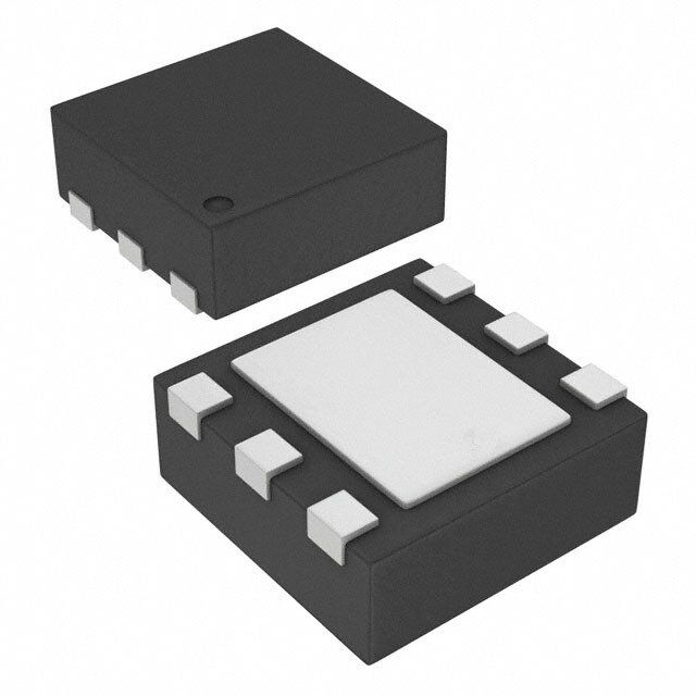
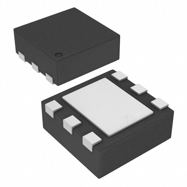
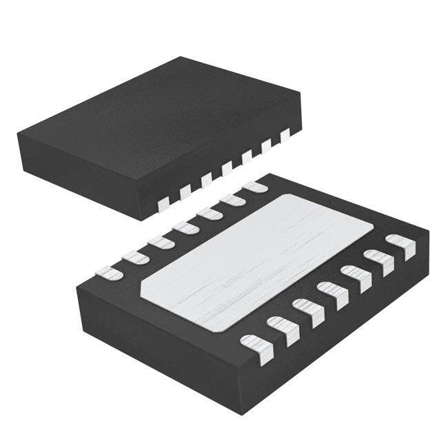
| 供应商器件封装 | 6-SON(2x2) |
| 其它名称 | 296-22981-1 |
| 内部驱动器 | 是 |
| 功率耗散 | 500 mW |
| 包装 | 剪切带 (CT) |
| 单位重量 | 9.700 mg |
| 商标 | Texas Instruments |
| 安装类型 | 表面贴装 |
| 安装风格 | SMD/SMT |
| 宽度 | 2 mm |
| 封装 | Reel |
| 封装/外壳 | 6-WDFN 裸露焊盘 |
| 封装/箱体 | WSON-6 |
| 工作温度 | -40°C ~ 85°C |
| 工作频率 | 1 MHz |
| 工厂包装数量 | 3000 |
| 恒压 | - |
| 恒流 | - |
| 拓扑 | PWM,升压(升压) |
| 拓扑结构 | Boost |
| 最大工作温度 | + 85 C |
| 最大电源电流 | 50 uA |
| 最小工作温度 | - 40 C |
| 标准包装 | 1 |
| 电压-电源 | 1.8 V ~ 6 V |
| 电压-输出 | 28V |
| 类型 | Inductive |
| 类型-初级 | 背光 |
| 类型-次级 | 白色 LED |
| 系列 | TPS61041 |
| 输入电压 | 1.8 V to 6 V |
| 输出数 | 1 |
| 输出电流 | 250 mA |
| 输出端数量 | 1 Output |
| 输出类型 | Current Mode |
| 配用 | /product-detail/zh/TPS61040EVM-002/296-20609-ND/562071/product-detail/zh/TPS61040EVM-001/296-13585-ND/486543 |
| 频率 | 1MHz |
| 高电平输出电流 | 0.05 A |


- 商务部:美国ITC正式对集成电路等产品启动337调查
- 曝三星4nm工艺存在良率问题 高通将骁龙8 Gen1或转产台积电
- 太阳诱电将投资9.5亿元在常州建新厂生产MLCC 预计2023年完工
- 英特尔发布欧洲新工厂建设计划 深化IDM 2.0 战略
- 台积电先进制程称霸业界 有大客户加持明年业绩稳了
- 达到5530亿美元!SIA预计今年全球半导体销售额将创下新高
- 英特尔拟将自动驾驶子公司Mobileye上市 估值或超500亿美元
- 三星加码芯片和SET,合并消费电子和移动部门,撤换高东真等 CEO
- 三星电子宣布重大人事变动 还合并消费电子和移动部门
- 海关总署:前11个月进口集成电路产品价值2.52万亿元 增长14.8%


PDF Datasheet 数据手册内容提取
Product Sample & Technical Tools & Support & Folder Buy Documents Software Community TPS61040,TPS61041 SLVS413I–OCTOBER2002–REVISEDDECEMBER2016 TPS6104x Low-Power DC-DC Boost Converter in SOT-23 and WSON Packages 1 Features 3 Description • 1.8-Vto6-VInputVoltageRange The TPS6104x is a high-frequency boost converter 1 dedicated for small to medium LCD bias supply and • AdjustableOutputVoltageRangeupto28V white LED backlight supplies. The device is ideal to • 400-mA(TPS61040)and250-mA(TPS61041) generate output voltages up to 28 V from a dual-cell InternalSwitchCurrent NiMH/NiCd or a single-cell Li-Ion battery. The part • Upto1-MHzSwitchingFrequency can also be used to generate standard 3.3-V or 5-V to12-Vpowerconversions. • 28-μATypicalNo-LoadQuiescentCurrent The TPS6104x operates with a switching frequency • 1-μATypicalShutdownCurrent up to 1 MHz. This frequency allows the use of small • InternalSoftStart external components using ceramic as well as • AvailableinSOT23-5,TSOT23-5, tantalum output capacitors. Together with the thin and2-mm×2-mm ×0.8-mmWSONPackages WSON package, the TPS6104x gives a very small overall solution size. The TPS61040 device has an 2 Applications internal 400-mA switch current limit, while the TPS61041 device has a 250-mA switch current limit, • LCDBiasSupply offering lower output voltage ripple and allows the • White-LEDSupplyforLCDBacklights use of a smaller form factor inductor for lower power • DigitalStillCamera applications. The low quiescent current (typically 28 μA) together with an optimized control scheme, • PDAs,Organizers,andHandheldPCs allows device operation at very high efficiencies over • CellularPhones theentireloadcurrentrange. • InternetAudioPlayers DeviceInformation(1) • Standard3.3-Vor5-Vto12-VConversion PARTNUMBER PACKAGE BODYSIZE(NOM) SOT-23(5) 2.90mm×1.60mm TPS61040 SOT(5) 2.90mm×1.60mm WSON(6) 2.00mm×2.00mm SOT-23(5) 2.90mm×1.60mm TPS61041 WSON(6) 2.00mm×2.00mm (1) For all available packages, see the orderable addendum at theendofthedatasheet. TypicalApplicationSchematic EfficiencyvsOutputCurrent L1 90 1.8 V to V6 IVN 10mH D1 VVOINUtTo 28 V 8868 VO=18V VI=5V CFF % 84 VI=3.6V 5 VIN SW 1 R1 CO ncy− 8802 e FB 3 1mF Effici 78 VI=2.4V CIN 76 4.7mF 4 2 EN GND R2 74 72 70 0.1 1 10 100 IO−Output Current−mA Copyright © 2016,Texas Instruments Incorporated 1 An IMPORTANT NOTICE at the end of this data sheet addresses availability, warranty, changes, use in safety-critical applications, intellectualpropertymattersandotherimportantdisclaimers.PRODUCTIONDATA.
TPS61040,TPS61041 SLVS413I–OCTOBER2002–REVISEDDECEMBER2016 www.ti.com Table of Contents 1 Features.................................................................. 1 8 ApplicationandImplementation........................ 11 2 Applications........................................................... 1 8.1 ApplicationInformation............................................11 3 Description............................................................. 1 8.2 TypicalApplication..................................................11 4 RevisionHistory..................................................... 2 8.3 SystemExamples...................................................16 5 PinConfigurationandFunctions......................... 3 9 PowerSupplyRecommendations...................... 19 6 Specifications......................................................... 4 10 Layout................................................................... 19 6.1 AbsoluteMaximumRatings......................................4 10.1 LayoutGuidelines.................................................19 6.2 ESDRatings..............................................................4 10.2 LayoutExample....................................................19 6.3 RecommendedOperatingConditions.......................4 11 DeviceandDocumentationSupport................. 20 6.4 ThermalInformation..................................................4 11.1 Third-PartyProductsDisclaimer...........................20 6.5 ElectricalCharacteristics...........................................5 11.2 RelatedLinks........................................................20 6.6 TypicalCharacteristics..............................................6 11.3 CommunityResources..........................................20 7 DetailedDescription.............................................. 9 11.4 Trademarks...........................................................20 7.1 Overview...................................................................9 11.5 ElectrostaticDischargeCaution............................20 7.2 FunctionalBlockDiagram.........................................9 11.6 Glossary................................................................20 7.3 FeatureDescription...................................................9 12 Mechanical,Packaging,andOrderable Information........................................................... 20 7.4 DeviceFunctionalModes........................................10 4 Revision History ChangesfromRevisionH(October2015)toRevisionI Page • ChangedC from:4.7mFTo:4.7µFandC From:1mFTo:1µFintheTypicalApplicationSchematic.......................... 1 IN O ChangesfromRevisionG(December2014)toRevisionH Page • Added500µs/divlabeltoX-axisofFigure15. ................................................................................................................... 15 ChangesfromRevisionF(December2010)toRevisionG Page • AddedESDRatingstable,FeatureDescriptionsection,DeviceFunctionalModes,ApplicationandImplementation section,PowerSupplyRecommendationssection,Layoutsection,DeviceandDocumentationSupportsection,and Mechanical,Packaging,andOrderableInformationsection.................................................................................................. 1 2 SubmitDocumentationFeedback Copyright©2002–2016,TexasInstrumentsIncorporated ProductFolderLinks:TPS61040 TPS61041
TPS61040,TPS61041 www.ti.com SLVS413I–OCTOBER2002–REVISEDDECEMBER2016 5 Pin Configuration and Functions DDCPackage,DBVPackage 5Pins TopView SW 1 5 VIN GND 2 FB 3 4 EN DRVPackage 6Pins TopView GND 1 6 SW VIN 2 5 NC EN 3 4 FB PinFunctions PIN DDC, I/O DESCRIPTION NAME DRVNO. DBVNO. Thisistheenablepinofthedevice.Pullingthispintogroundforcesthedeviceintoshutdown EN 4 3 I modereducingthesupplycurrenttolessthan1μA.Thispinshouldnotbeleftfloatingandneeds tobeterminated. Thisisthefeedbackpinofthedevice.Connectthispintotheexternalvoltagedividertoprogram FB 3 4 I thedesiredoutputvoltage. GND 2 1 – Ground NC – 5 – Noconnection ConnecttheinductorandtheSchottkydiodetothispin.Thisistheswitchpinandisconnectedto SW 1 6 I thedrainoftheinternalpowerMOSFET. V 5 2 I Supplyvoltagepin IN Copyright©2002–2016,TexasInstrumentsIncorporated SubmitDocumentationFeedback 3 ProductFolderLinks:TPS61040 TPS61041
TPS61040,TPS61041 SLVS413I–OCTOBER2002–REVISEDDECEMBER2016 www.ti.com 6 Specifications 6.1 Absolute Maximum Ratings overoperatingfree-airtemperaturerange(unlessotherwisenoted) (1) MIN MAX UNIT SupplyvoltagesonpinV (2) –0.3 7 V IN VoltagesonpinsEN,FB (2) –0.3 V +0.3 V IN SwitchvoltageonpinSW (2) 30 30 V Operatingjunctiontemperature,T –40 150 °C J Storagetemperature,T –65 150 °C stg (1) StressesbeyondthoselistedunderAbsoluteMaximumRatingsmaycausepermanentdamagetothedevice.Thesearestressratings only,whichdonotimplyfunctionaloperationofthedeviceattheseoranyotherconditionsbeyondthoseindicatedunderRecommended OperatingConditions.Exposuretoabsolute-maximum-ratedconditionsforextendedperiodsmayaffectdevicereliability. (2) Allvoltagevaluesarewithrespecttonetworkgroundterminal. 6.2 ESD Ratings VALUE UNIT Humanbodymodel(HBM),perANSI/ESDA/JEDECJS-001(1) ±2000 V(ESD) Electrostaticdischarge Charged-devicemodel(CDM),perJEDECspecificationJESD22- ±750 V C101(2) (1) JEDECdocumentJEP155statesthat500-VHBMallowssafemanufacturingwithastandardESDcontrolprocess.Manufacturingwith lessthan500-VHBMispossiblewiththenecessaryprecautions.Pinslistedas±XXXVmayactuallyhavehigherperformance. (2) JEDECdocumentJEP157statesthat250-VCDMallowssafemanufacturingwithastandardESDcontrolprocess.Manufacturingwith lessthan250-VCDMispossiblewiththenecessaryprecautions.Pinslistedas±YYYVmayactuallyhavehigherperformance. 6.3 Recommended Operating Conditions MIN NOM MAX UNIT V Inputvoltagerange 1.8 6 V IN V Outputvoltagerange 28 V OUT L Inductor(1) 2.2 10 μH f Switchingfrequency(1) 1 MHz C Inputcapacitor (1) 4.7 μF IN C Outputcapacitor (1) 1 μF OUT T Operatingambienttemperature –40 85 °C A T Operatingjunctiontemperature –40 125 °C J (1) Seeapplicationsectionforfurtherinformation. 6.4 Thermal Information TPS61040 TPS61041 THERMALMETRIC(1) DBV DDC DRV DBV DRV UNIT 5PINS 5PINS 6PINS 5PINS 6PINS R Junction-to-ambientthermalresistance 205.2 214.7 83.0 205.2 83.0 °C/W θJA R Junction-to-case(top)thermalresistance 118.3 38.5 57.1 118.3 57.1 °C/W θJC(top) R Junction-to-boardthermalresistance 34.8 35.4 52.9 34.8 52.9 °C/W θJB ψ Junction-to-topcharacterizationparameter 12.2 0.4 2.4 12.2 2.4 °C/W JT ψ Junction-to-boardcharacterizationparameter 33.9 34.8 53.4 33.9 53.4 °C/W JB R Junction-to-case(bottom)thermalresistance — — 26.9 — 26.9 °C/W θJC(bot) (1) Formoreinformationabouttraditionalandnewthermalmetrics,seetheICPackageThermalMetricsapplicationreport,SPRA953. 4 SubmitDocumentationFeedback Copyright©2002–2016,TexasInstrumentsIncorporated ProductFolderLinks:TPS61040 TPS61041
TPS61040,TPS61041 www.ti.com SLVS413I–OCTOBER2002–REVISEDDECEMBER2016 6.5 Electrical Characteristics V =2.4V,EN=V ,T =–40°Cto85°C,typicalvaluesareatT =25°C(unlessotherwisenoted) IN IN A A PARAMETER TESTCONDITIONS MIN TYP MAX UNIT SUPPLYCURRENT V Inputvoltagerange 1.8 6 V IN I Operatingquiescentcurrent I =0mA,notswitching,V =1.3V 28 50 μA Q OUT FB I Shutdowncurrent EN=GND 0.1 1 μA SD V Undervoltagelockoutthreshold 1.5 1.7 V UVLO ENABLE V ENhighlevelinputvoltage 1.3 V IH V ENlowlevelinputvoltage 0.4 V IL I ENinputleakagecurrent EN=GNDorV 0.1 1 μA I IN POWERSWITCHANDCURRENTLIMIT Vsw Maximumswitchvoltage 30 V t Minimumofftime 250 400 550 ns off t Maximumontime 4 6 7.5 μs on R MOSFETon-resistance V =2.4V;I =200mA;TPS61040 600 1000 mΩ DS(on) IN SW R MOSFETon-resistance V =2.4V;I =200mA;TPS61041 750 1250 mΩ DS(on) IN SW MOSFETleakagecurrent V =28V 1 10 μA SW I MOSFETcurrentlimit TPS61040 350 400 450 mA LIM I MOSFETcurrentlimit TPS61041 215 250 285 mA LIM OUTPUT V Adjustableoutputvoltagerange V 28 V OUT IN V Internalvoltagereference 1.233 V ref I Feedbackinputbiascurrent V =1.3V 1 μA FB FB V Feedbacktrippointvoltage 1.8V≤V ≤6V 1.208 1.233 1.258 V FB IN Lineregulation (1) 1.8V≤VIN≤6V;VOUT=18V;Iload=10mA; 0.05 %/V C =notconnected FF Loadregulation(1) V =2.4V;V =18V;0mA≤I ≤30mA 0.15 %/mA IN OUT OUT (1) Thelineandloadregulationdependontheexternalcomponentselection.Seetheapplicationsectionforfurtherinformation. Copyright©2002–2016,TexasInstrumentsIncorporated SubmitDocumentationFeedback 5 ProductFolderLinks:TPS61040 TPS61041
TPS61040,TPS61041 SLVS413I–OCTOBER2002–REVISEDDECEMBER2016 www.ti.com 6.6 Typical Characteristics Table1.TableofGraphs FIGURE Figure1, vsLoadcurrent Figure2, η Efficiency Figure3 vsInputvoltage Figure4 I Quiescentcurrent vsInputvoltageandtemperature Figure5 Q V Feedbackvoltage vsTemperature Figure6 FB I Switchcurrentlimit vsTemperature Figure7 SW vsSupplyvoltage,TPS61041 Figure8 I Switchcurrentlimit CL vsSupplyvoltage,TPS61040 Figure9 vsTemperature Figure10 R R DS(on) DS(on) vsSupplyvoltage Figure11 Linetransientresponse Figure13 Loadtransientresponse Figure14 Start-upbehavior Figure15 90 90 VO = 18 V L = 10 m H 88 VI = 5 V 88 VO = 18 V 86 86 TPS61040 84 VI = 3.6 V 84 Efficiency − % 788802 VI = 2.4 V Efficiency − % 788802 TPS61041 76 76 74 74 72 72 70 70 0.1 1 10 100 0.1 1 10 100 IO − Output Current − mA IL − Load Current − mA Figure1.EfficiencyvsOutputCurrent Figure2.EfficiencyvsLoadCurrent 90 90 88 VO = 18 V 88 VL O= =1 01 8m HV IO = 10 mA 86 L = 10 m H 86 84 84 IO = 5 mA − % 82 L = 3.3 m H − % 82 y y nc 80 nc 80 e e ci ci Effi 78 Effi 78 76 76 74 74 72 72 70 70 0.1 1 10 100 1 2 3 4 5 6 IL − Load Current − mA VI − Input Voltage − V Figure3.EfficiencyvsLoadCurrent Figure4.EfficiencyvsInputVoltage 6 SubmitDocumentationFeedback Copyright©2002–2016,TexasInstrumentsIncorporated ProductFolderLinks:TPS61040 TPS61041
TPS61040,TPS61041 www.ti.com SLVS413I–OCTOBER2002–REVISEDDECEMBER2016 40 1.24 35 TA = 85°C 1.238 mQuiescent Current − A 1122305050 TTAA == −2470°C°C V − Feedback Voltage − VFB 11..223346 VCC = 2.4 V 1.232 5 0 1.23 1.8 2.4 3 3.6 4.2 4.8 5.4 6 −40 −20 0 20 40 60 80 100 120 VI − Input Voltage − V TA − Temperature − °C Figure5.TPS61040QuiescentCurrentvsInputVoltage Figure6.FeedbackVoltagevsFree-AirTemperature 430 260 410 TPS61040 258 mA 390 256 − A urrent Limit 333357000 nt Limit − m 222555024 TA = 27°C witch C 310 − Curre 248 − S 290 CL) 246 W) I( I(S 270 TPS61041 244 250 242 230 240 −40−30−20−10 0 10 20 30 40 50 60 70 80 90 1.8 2.4 3 3.6 4.2 4.8 5.4 6 TA − Temperature − °C VCC − Supply Voltage − V Figure7.TPS6104xSwitchCurrentLimitvsFree-Air Figure8.TPS61041CurrentLimitvsSupplyVoltage Temperature 420 1200 Wm − 415 e nc 1000 a A 410 sist TPS61041 nt Limit − m 440005 TA = 27°C On-State Re 680000 TPS61040 I − Curre(CL) 339905 Drain-Source 400 c 385 Stati 200 − 3801.8 2.4 3 3.6 4.2 4.8 5.4 6 DS(on) −040−30−20−10 0 10 20 30 40 50 60 70 80 90 VCC − Supply Voltage − V r TA − Temperature − °C Figure9.TPS61040CurrentLimitvsSupplyVoltage Figure10.TPS6104xStaticDrain-SourceOn-State ResistancevsFree-AirTemperature Copyright©2002–2016,TexasInstrumentsIncorporated SubmitDocumentationFeedback 7 ProductFolderLinks:TPS61040 TPS61041
TPS61040,TPS61041 SLVS413I–OCTOBER2002–REVISEDDECEMBER2016 www.ti.com 1000 Wm e − 900 c n sista 800 TPS61041 Re 700 e Stat 600 On- 500 TPS61040 e c ur 400 o S ain- 300 Dr c 200 ati − St 100 DS(on) 01.8 2.4 3 3.6 4.2 4.8 5.4 6 r VCC − Supply Voltage − V Figure11.TPS6104xStaticDrain-SourceOn-StateResistancevsSupplyVoltage 8 SubmitDocumentationFeedback Copyright©2002–2016,TexasInstrumentsIncorporated ProductFolderLinks:TPS61040 TPS61041
TPS61040,TPS61041 www.ti.com SLVS413I–OCTOBER2002–REVISEDDECEMBER2016 7 Detailed Description 7.1 Overview The TPS6104x is a high-frequency boost converter dedicated for small to medium LCD bias supply and white LED backlight supplies. The device is ideal to generate output voltages up to 28 V from a dual-cell NiMH/NiCd or asinglecelldeviceLi-Ionbattery. 7.2 Functional Block Diagram SW Under Voltage VIN Lockout Bias Supply 400 ns Min OffTime Error Comparator FB - S Power MOSFET + RS Latch Gate N-Channel Logic Driver VREF= 1.233 V R Current Limit 6ms Max + RSENSE EN OnTime _ Soft Start GND Copyright © 2016,Texas Instruments Incorporated 7.3 Feature Description 7.3.1 PeakCurrentControl The internal switch turns on until the inductor current reaches the typical dc current limit (I ) of 400 mA LIM (TPS61040) or 250 mA (TPS61041). Due to the internal propagation delay of typical 100 ns, the actual current exceedsthedccurrentlimitthresholdbyasmallamount.Thetypicalpeakcurrentlimitcanbecalculated: V I = I + IN × 100ns peak(typ) LIM L V I = 400mA + IN × 100ns for theTPS61040-Q1 peak(typ) L V I = 250mA + IN × 100ns for theTPS61041-Q1 peak(typ) L (1) Thehighertheinputvoltageandthelowertheinductorvalue,thegreaterthepeak. By selecting the TPS6104x, it is possible to tailor the design to the specific application current limit requirements. A lower current limit supports applications requiring lower output power and allows the use of an inductor with a lower current rating and a smaller form factor. A lower current limit usually has a lower output voltage ripple as well. Copyright©2002–2016,TexasInstrumentsIncorporated SubmitDocumentationFeedback 9 ProductFolderLinks:TPS61040 TPS61041
TPS61040,TPS61041 SLVS413I–OCTOBER2002–REVISEDDECEMBER2016 www.ti.com Feature Description (continued) 7.3.2 SoftStart All inductive step-up converters exhibit high inrush current during start-up if no special precaution is made. This can cause voltage drops at the input rail during start up and may result in an unwanted or early system shut down. I LIM 4 The TPS6104x limits this inrush current by increasing the current limit in two steps starting from for 256 I LIM 2 cyclesto forthenext256cycles,andthenfullcurrentlimit(seeFigure15). 7.3.3 Enable Pulling the enable (EN) to ground shuts down the device reducing the shutdown current to 1 μA (typical). Because there is a conductive path from the input to the output through the inductor and Schottky diode, the output voltage is equal to the input voltage during shutdown. The enable pin needs to be terminated and should not be left floating. Using a small external transistor disconnects the input from the output during shutdown as showninFigure17. 7.3.4 UndervoltageLockout An undervoltage lockout prevents misoperation of the device at input voltages below typical 1.5 V. When the inputvoltageisbelowtheundervoltagethreshold,themainswitchisturnedoff. 7.3.5 ThermalShutdown An internal thermal shutdown is implemented and turns off the internal MOSFETs when the typical junction temperature of 168°C is exceeded. The thermal shutdown has a hysteresis of typically 25°C. This data is based onstatisticalmeansandisnottestedduringtheregularmassproductionoftheIC. 7.4 Device Functional Modes 7.4.1 Operation The TPS6104x operates with an input voltage range of 1.8 V to 6 V and can generate output voltages up to 28 V. The device operates in a pulse-frequency-modulation (PFM) scheme with constant peak current control. This control scheme maintains high efficiency over the entire load current range, and with a switching frequency up to 1MHz,thedeviceenablestheuseofverysmallexternalcomponents. Theconvertermonitorstheoutputvoltage,andassoonasthefeedbackvoltagefallsbelowthereferencevoltage of typically 1.233 V, the internal switch turns on and the current ramps up. The switch turns off as soon as the inductor current reaches the internally set peak current of typically 400 mA (TPS61040) or 250 mA (TPS61041). See Peak Current Control for more information. The second criteria that turns off the switch is the maximum on- time of 6 μs (typical). This is just to limit the maximum on-time of the converter to cover for extreme conditions. As the switch is turned off the external Schottky diode is forward biased delivering the current to the output. The switch remains off for a minimum of 400 ns (typical), or until the feedback voltage drops below the reference voltage again. Using this PFM peak current control scheme the converter operates in discontinuous conduction mode (DCM) where the switching frequency depends on the output current, which results in very high efficiency over the entire load current range. This regulation scheme is inherently stable, allowing a wider selection range fortheinductorandoutputcapacitor. 10 SubmitDocumentationFeedback Copyright©2002–2016,TexasInstrumentsIncorporated ProductFolderLinks:TPS61040 TPS61041
TPS61040,TPS61041 www.ti.com SLVS413I–OCTOBER2002–REVISEDDECEMBER2016 8 Application and Implementation NOTE Information in the following applications sections is not part of the TI component specification, and TI does not warrant its accuracy or completeness. TI’s customers are responsible for determining suitability of components for their purposes. Customers should validateandtesttheirdesignimplementationtoconfirmsystemfunctionality. 8.1 Application Information The TPS6104x is designed for output voltages up to 28 V with an input voltage range of 1.8 V to 6 V and a switch peak current limit of 400 mA (250 mA for the TPS61041). The device operates in a pulse-frequency- modulation (PFM) scheme with constant peak current control. This control scheme maintains high efficiency over the entire load current range, and with a switching frequency up to 1 MHz, the device enables the use of very small external components. The following section provides a step-by-step design approach for configuring the TPS61040asavoltageregulatingboostconverterforLCDbiaspowersupply,asshowninFigure12. 8.2 Typical Application The following section provides a step-by-step design approach for configuring the TPS611040 as a voltage regulatingboostconverterforLCDbiassupply,asshowninFigure12. L1 D1 10μH VIN VOUT 1.8 V to 6 V 18 V TPS61040 R1 CFF VIN SW 2.2 MΩ 22 pF C2 1μF FB C1 L1: Sumida CR32-100 4.7μF EN GND R2 D1:Motorola MBR0530 160 kΩ C1:TayoYuden JMK212BY475MG C2:TayoYudenTMK316BJ105KL Copyright © 2016,Texas Instruments Incorporated Figure12. LCDBiasSupply 8.2.1 DesignRequirements Table2.DesignParameters DESIGNPARAMETER EXAMPLEVALUE InputVoltage 1.8Vto6V OutputVoltage 18V OutputCurrent 10mA 8.2.2 DetailedDesignProcedure 8.2.2.1 InductorSelection,MaximumLoadCurrent BecausethePFMpeakcurrentcontrolschemeisinherentlystable,theinductorvaluedoesnotaffectthestability of the regulator. The selection of the inductor together with the nominal load current, input and output voltage of the application determines the switching frequency of the converter. Depending on the application, inductor values from 2.2μH to 47 μH are recommended. The maximum inductor value is determined by the maximum on time of the switch, typically 6 μs. The peak current limit of 400 mA/250 mA (typically) should be reached within this6-μsperiodforproperoperation. Copyright©2002–2016,TexasInstrumentsIncorporated SubmitDocumentationFeedback 11 ProductFolderLinks:TPS61040 TPS61041
TPS61040,TPS61041 SLVS413I–OCTOBER2002–REVISEDDECEMBER2016 www.ti.com The inductor value determines the maximum switching frequency of the converter. Therefore, select the inductor value that ensures the maximum switching frequency at the converter maximum load current is not exceeded. Themaximumswitchingfrequencyiscalculatedbythefollowingformula: V ´(V -V ) f = IN(min) OUT IN S(max) I ´L´V P OUT where • I =PeakcurrentasdescribedinPeakCurrentControl P • L=Selectedinductorvalue • V =Thehighestswitchingfrequencyoccursattheminimuminputvoltage (2) IN(min) If the selected inductor value does not exceed the maximum switching frequency of the converter, the next step istocalculatetheswitchingfrequencyatthenominalloadcurrentusingthefollowingformula: 2´I ´(V -V +V ) f (I )= load OUT IN d S load I 2´L P where • I =PeakcurrentasdescribedinPeakCurrentControl P • L=Selectedinductorvalue • I =Nominalloadcurrent load • Vd=Rectifierdiodeforwardvoltage(typically0.3V) (3) Asmallerinductorvaluegivesahigherconverterswitchingfrequency,butlowerstheefficiency. The inductor value has less effect on the maximum available load current and is only of secondary order. The best way to calculate the maximum available load current under certain operating conditions is to estimate the expected converter efficiency at the maximum load current. This number can be taken out of the efficiency graphsshowninFigure1throughFigure4.Themaximumloadcurrentcanthenbeestimatedasfollows: I 2 ´L ´ f P S(max) I = h load(max) 2´(V - V ) OUT IN where • I =PeakcurrentasdescribedinPeakCurrentControl P • L=Selectedinductorvalue • fS =Maximumswitchingfrequencyascalculatedpreviously max • η=Expectedconverterefficiency.Typically70%to85% (4) The maximum load current of the converter is the current at the operation point where the converter starts to enter the continuous conduction mode. Usually the converter should always operate in discontinuous conduction mode. Last, the selected inductor should have a saturation current that meets the maximum peak current of the converter(ascalculatedinPeakCurrentControl).UsethemaximumvalueforI forthiscalculation. LIM Another important inductor parameter is the dc resistance. The lower the dc resistance, the higher the efficiency oftheconverter.SeeTable3andthetypicalapplicationsfortheinductorselection. Table3.RecommendedInductorforTypicalLCDBiasSupply(seeFigure23) DEVICE INDUCTORVALUE COMPONENTSUPPLIER COMMENTS 10μH SumidaCR32-100 Highefficiency 10μH SumidaCDRH3D16-100 Highefficiency TPS61040 10μH MurataLQH4C100K04 Highefficiency 4.7μH SumidaCDRH3D16-4R7 Smallsolutionsize 4.7μH MurataLQH3C4R7M24 Smallsolutionsize Highefficiency TPS61041 10μH MurataLQH3C100K24 Smallsolutionsize 12 SubmitDocumentationFeedback Copyright©2002–2016,TexasInstrumentsIncorporated ProductFolderLinks:TPS61040 TPS61041
TPS61040,TPS61041 www.ti.com SLVS413I–OCTOBER2002–REVISEDDECEMBER2016 8.2.2.2 SettingtheOutputVoltage Theoutputvoltageiscalculatedas: (cid:4) R1(cid:5) VOUT(cid:3)1.233V(cid:1) 1(cid:2)R2 (5) For battery-powered applications, a high-impedance voltage divider should be used with a typical value for R2 of ≤200 kΩ and a maximum value for R1 of 2.2 MΩ. Smaller values might be used to reduce the noise sensitivity of thefeedbackpin. A feedforward capacitor across the upper feedback resistor R1 is required to provide sufficient overdrive for the errorcomparator.Withoutafeedforwardcapacitor,oronewhosevalueistoosmall,theTPS6104xshows double pulses or a pulse burst instead of single pulses at the switch node (SW), causing higher output voltage ripple. If thishigheroutputvoltagerippleisacceptable,thefeedforwardcapacitorcanbeleftout. The lower the switching frequency of the converter, the larger the feedforward capacitor value required. A good startingpointistousea10-pFfeedforwardcapacitor.Asafirstestimation,therequiredvalueforthefeedforward capacitorattheoperationpointcanalsobecalculatedusingthefollowingformula: C (cid:2) 1 FF 2(cid:1)(cid:1)(cid:1) fS(cid:1)R1 20 where • R1=Upperresistorofvoltagedivider • fS=Switchingfrequencyoftheconverteratthenominalloadcurrent(SeeInductorSelection,MaximumLoad Currentforcalculatingtheswitchingfrequency) • C =Chooseavaluethatcomesclosesttotheresultofthecalculation (6) FF The larger the feedforward capacitor the worse the line regulation of the device. Therefore, when concern for line regulation is paramount, the selected feedforward capacitor should be as small as possible. See the following sectionformoreinformationaboutlineandloadregulation. 8.2.2.3 LineandLoadRegulation The line regulation of the TPS6104x depends on the voltage ripple on the feedback pin. Usually a 50 mV peak- to-peakvoltagerippleonthefeedbackpinFBgivesgoodresults. Some applications require a very tight line regulation and can only allow a small change in output voltage over a certain input voltage range. If no feedforward capacitor C is used across the upper resistor of the voltage FF feedback divider, the device has the best line regulation. Without the feedforward capacitor the output voltage ripple is higher because the TPS6104x shows output voltage bursts instead of single pulses on the switch pin (SW), increasing the output voltage ripple. Increasing the output capacitor value reduces the output voltage ripple. If a larger output capacitor value is not an option, a feedforward capacitor C can be used as described in the FF previous section. The use of a feedforward capacitor increases the amount of voltage ripple present on the feedback pin (FB). The greater the voltage ripple on the feedback pin (≥50 mV), the worse the line regulation. Therearetwowaystoimprovethelineregulationfurther: 1. Use a smaller inductor value to increase the switching frequency which will lower the output voltage ripple, aswellasthevoltagerippleonthefeedbackpin. 2. Add a small capacitor from the feedback pin (FB) to ground to reduce the voltage ripple on the feedback pin down to 50 mV again. As a starting point, the same capacitor value as selected for the feedforward capacitor C canbeused. FF 8.2.2.4 OutputCapacitorSelection For best output voltage filtering, a low ESR output capacitor is recommended. Ceramic capacitors have a low ESRvaluebuttantalumcapacitorscanbeusedaswell,dependingontheapplication. Assuming the converter does not show double pulses or pulse bursts on the switch node (SW), the output voltageripplecanbecalculatedas: Copyright©2002–2016,TexasInstrumentsIncorporated SubmitDocumentationFeedback 13 ProductFolderLinks:TPS61040 TPS61041
TPS61040,TPS61041 SLVS413I–OCTOBER2002–REVISEDDECEMBER2016 www.ti.com (cid:1)Vout(cid:3)CIoouutt(cid:1)(cid:4)fS(I1out)–VoutIP(cid:2)(cid:1)VdL–Vin(cid:5)(cid:2)IP(cid:1)ESR where • I =PeakcurrentasdescribedinPeakCurrentControl P • L=Selectedinductorvalue • I =Nominalloadcurrent out • fS(I )=Switchingfrequencyatthenominalloadcurrentascalculatedpreviously out • Vd=Rectifierdiodeforwardvoltage(typically0.3V) • C =Selectedoutputcapacitor out • ESR=OutputcapacitorESRvalue (7) SeeTable4andtheTypicalApplicationforchoosingtheoutputcapacitor. Table4.RecommendedInputandOutputCapacitors DEVICE CAPACITOR VOLTAGERATING COMPONENTSUPPLIER(1) COMMENTS 4.7μF/X5R/0805 6.3V TayoYudenJMK212BY475MG C /C IN OUT 10μF/X5R/0805 6.3V TayoYudenJMK212BJ106MG C /C IN OUT TPS6104x 1μF/X7R/1206 25V TayoYudenTMK316BJ105KL C OUT 1μF/X5R/1206 35V TayoYudenGMK316BJ105KL C OUT 4.7μF/X5R/1210 25V TayoYudenTMK325BJ475MG C OUT (1) SeeThird-PartyProductsdisclaimer. 8.2.2.5 InputCapacitorSelection For good input voltage filtering, low ESR ceramic capacitors are recommended. A 4.7-μF ceramic input capacitor issufficientformostoftheapplications.Forbetterinputvoltagefilteringthisvaluecanbeincreased.SeeTable4 andtypicalapplicationsforinputcapacitorrecommendations. 8.2.2.6 DiodeSelection To achieve high efficiency a Schottky diode should be used. The current rating of the diode should meet the peak current rating of the converter as it is calculated in Peak Current Control. Use the maximum value for I LIM forthiscalculation.SeeTable5andthetypicalapplicationsfortheselectionoftheSchottkydiode. Table5.RecommendedSchottkyDiodeforTypicalLCDBiasSupply(seeFigure23) DEVICE REVERSEVOLTAGE COMPONENTSUPPLIER(1) COMMENTS 30V ONSemiconductorMBR0530 20V ONSemiconductorMBR0520 TPS6104x 20V ONSemiconductorMBRM120L Highefficiency 30V ToshibaCRS02 spacer (1) SeeThird-PartyProductsdisclaimer. 14 SubmitDocumentationFeedback Copyright©2002–2016,TexasInstrumentsIncorporated ProductFolderLinks:TPS61040 TPS61041
TPS61040,TPS61041 www.ti.com SLVS413I–OCTOBER2002–REVISEDDECEMBER2016 8.2.3 ApplicationCurves VO = 18 V IO= 18 V VI 2.4 V to 3.4 V IO 100 mV/div VO IO 100 mV/div 1 mAto 10 mA 200mS/div 200 m S/div Figure13.LineTransientResponse Figure14.LoadTransientResponse V = 18 V O V O 5 V/div EN 1 V/div I I 50 mA/div 500 us/div Figure15.Start-UpBehavior Copyright©2002–2016,TexasInstrumentsIncorporated SubmitDocumentationFeedback 15 ProductFolderLinks:TPS61040 TPS61041
TPS61040,TPS61041 SLVS413I–OCTOBER2002–REVISEDDECEMBER2016 www.ti.com 8.3 System Examples L1 D1 10μH VO 18 V TPS61040 CFF R1 22 pF VIN VIN SW 2.2 MΩ 1.8 V to 6 V C2 1μF FB C1 4.7μF DAC orAnalog Voltage EN GND R2 0 V = 25 V 160 kΩ 1.233 V = 18 V L1: Sumida CR32-100 D1:Motorola MBR0530 C1:TayoYuden JMK212BY475MG C2:TayoYuden GMK316BJ105KL Copyright © 2016,Texas Instruments Incorporated Figure16. LCDBiasSupplyWithAdjustableOutputVoltage R3 200 k L1 BC857C 10μH D1 VIN VOUT 1.8 V to 6 V 18 V / 10 mA TPS61040 R1 CFF 2.2 MΩ 22 pF VIN SW C2 C3 1μF 0.1μF FB (Optional) C1 4.7μF EN GND R2 L1:Sumida CR32-100 160 kΩ D1:Motorola MBR0530 C1:TayoYuden JMK212BY475MG C2:TayoYudenTMK316BJ105KL Copyright © 2016,Texas Instruments Incorporated Figure17. LCDBiasSupplyWithLoadDisconnect 16 SubmitDocumentationFeedback Copyright©2002–2016,TexasInstrumentsIncorporated ProductFolderLinks:TPS61040 TPS61041
TPS61040,TPS61041 www.ti.com SLVS413I–OCTOBER2002–REVISEDDECEMBER2016 System Examples (continued) D3 V2 =–10 V/15μA D2 C4 C3 4.7μF 1μF L1 D1 6.8μH V1 = 10 V/15 mA TPS61040 CFF VIN= 2.7 V to 5 V VIN SW 1.5 MRΩ1 22 pF C2 1μF FB C1 L1: Murata LQH4C6R8M04 4.7μF EN GND R2 D1, D2, D3: Motorola MBR0530 C1: TayoYuden JMK212BY475MG 210 kΩ C2, C3, C4: TayoYuden EMK316BJ105KF Copyright © 2016,Texas Instruments Incorporated Figure18. PositiveandNegativeOutputLCDBiasSupply L1 D1 6.8μH VO=12 V/35 mA TPS61040 CFF R1 4.7 pF VIN3.3 V VIN SW 1.8 MΩ C2 4.7μF FB C1 10μF EN GND R2 L1: Murata LQH4C6R8M04 205 kΩ D1: Motorola MBR0530 C1: TayoYuden JMK212BJ106MG C2: TayoYuden EMK316BJ475ML Copyright © 2016,Texas Instruments Incorporated Figure19. Standard3.3-Vto12-VSupply 3.3μH D1 5 V/45 mA TPS61040 CFF 3.3 pF R1 1.8 V to 4 V VIN SW 620 kΩ C2 FB 4.7μF C1 4.7μF R2 EN GND 200 kΩ L1:Murata LQH4C3R3M04 D1:Motorola MBR0530 C1, C2:TayoYuden JMK212BY475MG Copyright © 2016,Texas Instruments Incorporated Figure20. DualBatteryCellto5-V/50-mAConversion EfficiencyApproximatelyEquals84%atV =2.4VtoVo=5V/45mA IN Copyright©2002–2016,TexasInstrumentsIncorporated SubmitDocumentationFeedback 17 ProductFolderLinks:TPS61040 TPS61041
TPS61040,TPS61041 SLVS413I–OCTOBER2002–REVISEDDECEMBER2016 www.ti.com System Examples (continued) L1 10μH D1 VCC= 2.7 V to 6 V D2 VIN SW 24 V (Optional) C1 FB 4.7μF C2 L1:Murata LQH4C100K04 PWM EN GND 1μF RS D1:Motorola MBR0530 100 Hz to 500 Hz 82Ω C1:TayoYuden JMK212BY475MG C2:TayoYudenTMK316BJ105KL Copyright © 2016,Texas Instruments Incorporated Figure21. WhiteLEDSupplyWithAdjustableBrightnessControl UsingaPWMSignalontheEnablePin,EfficiencyApproximatelyEquals86%atV =3V,I =15mA IN LED D1 L1 MBRM120L 10μH VCC= 2.7 V to 6 V D2 C2 VIN SW 24 V 100 nF (Optional) (See NoteA) FB C1 4.7μF R1 EN GND 120 kΩ RS 110Ω L1: Murata LQH4C3R3M04 D1:Motorola MBR0530 Analog Brightness Control C1:TayoYuden JMK212BY475MG 3.3 V@Led Off R2 C2:Standard Ceramic Capacitor 0 V@Iled = 20 mA 160 kΩ Copyright © 2016,Texas Instruments Incorporated A. AsmalleroutputcapacitorvalueforC2causesalargerLEDripple. Figure22. WhiteLEDSupplyWithAdjustableBrightnessControl UsinganAnalogSignalontheFeedbackPin 18 SubmitDocumentationFeedback Copyright©2002–2016,TexasInstrumentsIncorporated ProductFolderLinks:TPS61040 TPS61041
TPS61040,TPS61041 www.ti.com SLVS413I–OCTOBER2002–REVISEDDECEMBER2016 9 Power Supply Recommendations The device is designed to operate from an input voltage supply range between 1.8 V and 6 V. The output current of the input power supply must be rated according to the supply voltage, output voltage and output current of TPS6104x. 10 Layout 10.1 Layout Guidelines Typical for all switching power supplies, the layout is an important step in the design; especially at high peak currents and switching frequencies. If the layout is not carefully done, the regulator might show noise problems anddutycyclejitter. The input capacitor should be placed as close as possible to the input pin for good input voltage filtering. The inductor and diode should be placed as close as possible to the switch pin to minimize the noise coupling into other circuits. Because the feedback pin and network is a high-impedance circuit, the feedback network should be routed away from the inductor. The feedback pin and feedback network should be shielded with a ground planeortracetominimizenoisecouplingintothiscircuit. Wide traces should be used for connections in bold as shown in Figure 23. A star ground connection or ground planeminimizesgroundshiftsandnoise. 10.2 Layout Example VOUT VIN SW 1 5 VIN T P S GND 2 6 1 0 4 FB 3 0 4 EN GND Figure23. LayoutDiagram Copyright©2002–2016,TexasInstrumentsIncorporated SubmitDocumentationFeedback 19 ProductFolderLinks:TPS61040 TPS61041
TPS61040,TPS61041 SLVS413I–OCTOBER2002–REVISEDDECEMBER2016 www.ti.com 11 Device and Documentation Support 11.1 Third-Party Products Disclaimer TI'S PUBLICATION OF INFORMATION REGARDING THIRD-PARTY PRODUCTS OR SERVICES DOES NOT CONSTITUTE AN ENDORSEMENT REGARDING THE SUITABILITY OF SUCH PRODUCTS OR SERVICES OR A WARRANTY, REPRESENTATION OR ENDORSEMENT OF SUCH PRODUCTS OR SERVICES, EITHER ALONEORINCOMBINATIONWITHANYTIPRODUCTORSERVICE. 11.2 Related Links The table below lists quick access links. Categories include technical documents, support and community resources,toolsandsoftware,andquickaccesstosampleorbuy. Table6.RelatedLinks TECHNICAL TOOLS& SUPPORT& PARTS PRODUCTFOLDER SAMPLE&BUY DOCUMENTS SOFTWARE COMMUNITY TPS61041 Clickhere Clickhere Clickhere Clickhere Clickhere TPS61040 Clickhere Clickhere Clickhere Clickhere Clickhere 11.3 Community Resources The following links connect to TI community resources. Linked contents are provided "AS IS" by the respective contributors. They do not constitute TI specifications and do not necessarily reflect TI's views; see TI's Terms of Use. TIE2E™OnlineCommunity TI'sEngineer-to-Engineer(E2E)Community.Createdtofostercollaboration amongengineers.Ate2e.ti.com,youcanaskquestions,shareknowledge,exploreideasandhelp solveproblemswithfellowengineers. DesignSupport TI'sDesignSupport QuicklyfindhelpfulE2Eforumsalongwithdesignsupporttoolsand contactinformationfortechnicalsupport. 11.4 Trademarks E2EisatrademarkofTexasInstruments. Allothertrademarksarethepropertyoftheirrespectiveowners. 11.5 Electrostatic Discharge Caution Thesedeviceshavelimitedbuilt-inESDprotection.Theleadsshouldbeshortedtogetherorthedeviceplacedinconductivefoam duringstorageorhandlingtopreventelectrostaticdamagetotheMOSgates. 11.6 Glossary SLYZ022—TIGlossary. Thisglossarylistsandexplainsterms,acronyms,anddefinitions. 12 Mechanical, Packaging, and Orderable Information The following pages include mechanical, packaging, and orderable information. This information is the most current data available for the designated devices. This data is subject to change without notice and revision of thisdocument.Forbrowser-basedversionsofthisdatasheet,refertotheleft-handnavigation. 20 SubmitDocumentationFeedback Copyright©2002–2016,TexasInstrumentsIncorporated ProductFolderLinks:TPS61040 TPS61041
PACKAGE OPTION ADDENDUM www.ti.com 24-Aug-2018 PACKAGING INFORMATION Orderable Device Status Package Type Package Pins Package Eco Plan Lead/Ball Finish MSL Peak Temp Op Temp (°C) Device Marking Samples (1) Drawing Qty (2) (6) (3) (4/5) TPS61040DBVR ACTIVE SOT-23 DBV 5 3000 Green (RoHS CU NIPDAU | CU SN Level-1-260C-UNLIM -40 to 85 PHOI & no Sb/Br) TPS61040DBVRG4 ACTIVE SOT-23 DBV 5 3000 Green (RoHS CU SN Level-1-260C-UNLIM -40 to 85 PHOI & no Sb/Br) TPS61040DDCR ACTIVE SOT-23-THIN DDC 5 3000 Green (RoHS CU NIPDAU Level-2-260C-1 YEAR -40 to 85 QXK & no Sb/Br) TPS61040DDCT ACTIVE SOT-23-THIN DDC 5 250 Green (RoHS CU NIPDAU Level-2-260C-1 YEAR -40 to 85 QXK & no Sb/Br) TPS61040DRVR ACTIVE WSON DRV 6 3000 Green (RoHS CU NIPDAU Level-1-260C-UNLIM -40 to 85 CCL & no Sb/Br) TPS61040DRVT ACTIVE WSON DRV 6 250 Green (RoHS CU NIPDAU Level-1-260C-UNLIM -40 to 85 CCL & no Sb/Br) TPS61040DRVTG4 ACTIVE WSON DRV 6 250 Green (RoHS CU NIPDAU Level-1-260C-UNLIM -40 to 85 CCL & no Sb/Br) TPS61041DBVR ACTIVE SOT-23 DBV 5 3000 Green (RoHS CU NIPDAU Level-1-260C-UNLIM -40 to 85 PHPI & no Sb/Br) TPS61041DRVR ACTIVE WSON DRV 6 3000 Green (RoHS CU NIPDAU Level-1-260C-UNLIM -40 to 85 CAW & no Sb/Br) TPS61041DRVT ACTIVE WSON DRV 6 250 Green (RoHS CU NIPDAU Level-1-260C-UNLIM -40 to 85 CAW & no Sb/Br) TPS61041DRVTG4 ACTIVE WSON DRV 6 250 Green (RoHS CU NIPDAU Level-1-260C-UNLIM -40 to 85 CAW & no Sb/Br) (1) The marketing status values are defined as follows: ACTIVE: Product device recommended for new designs. LIFEBUY: TI has announced that the device will be discontinued, and a lifetime-buy period is in effect. NRND: Not recommended for new designs. Device is in production to support existing customers, but TI does not recommend using this part in a new design. PREVIEW: Device has been announced but is not in production. Samples may or may not be available. OBSOLETE: TI has discontinued the production of the device. (2) RoHS: TI defines "RoHS" to mean semiconductor products that are compliant with the current EU RoHS requirements for all 10 RoHS substances, including the requirement that RoHS substance do not exceed 0.1% by weight in homogeneous materials. Where designed to be soldered at high temperatures, "RoHS" products are suitable for use in specified lead-free processes. TI may reference these types of products as "Pb-Free". RoHS Exempt: TI defines "RoHS Exempt" to mean products that contain lead but are compliant with EU RoHS pursuant to a specific EU RoHS exemption. Green: TI defines "Green" to mean the content of Chlorine (Cl) and Bromine (Br) based flame retardants meet JS709B low halogen requirements of <=1000ppm threshold. Antimony trioxide based flame retardants must also meet the <=1000ppm threshold requirement. Addendum-Page 1
PACKAGE OPTION ADDENDUM www.ti.com 24-Aug-2018 (3) MSL, Peak Temp. - The Moisture Sensitivity Level rating according to the JEDEC industry standard classifications, and peak solder temperature. (4) There may be additional marking, which relates to the logo, the lot trace code information, or the environmental category on the device. (5) Multiple Device Markings will be inside parentheses. Only one Device Marking contained in parentheses and separated by a "~" will appear on a device. If a line is indented then it is a continuation of the previous line and the two combined represent the entire Device Marking for that device. (6) Lead/Ball Finish - Orderable Devices may have multiple material finish options. Finish options are separated by a vertical ruled line. Lead/Ball Finish values may wrap to two lines if the finish value exceeds the maximum column width. Important Information and Disclaimer:The information provided on this page represents TI's knowledge and belief as of the date that it is provided. TI bases its knowledge and belief on information provided by third parties, and makes no representation or warranty as to the accuracy of such information. Efforts are underway to better integrate information from third parties. TI has taken and continues to take reasonable steps to provide representative and accurate information but may not have conducted destructive testing or chemical analysis on incoming materials and chemicals. TI and TI suppliers consider certain information to be proprietary, and thus CAS numbers and other limited information may not be available for release. In no event shall TI's liability arising out of such information exceed the total purchase price of the TI part(s) at issue in this document sold by TI to Customer on an annual basis. OTHER QUALIFIED VERSIONS OF TPS61040, TPS61041 : •Automotive: TPS61040-Q1, TPS61041-Q1 NOTE: Qualified Version Definitions: •Automotive - Q100 devices qualified for high-reliability automotive applications targeting zero defects Addendum-Page 2
PACKAGE MATERIALS INFORMATION www.ti.com 8-May-2018 TAPE AND REEL INFORMATION *Alldimensionsarenominal Device Package Package Pins SPQ Reel Reel A0 B0 K0 P1 W Pin1 Type Drawing Diameter Width (mm) (mm) (mm) (mm) (mm) Quadrant (mm) W1(mm) TPS61040DBVR SOT-23 DBV 5 3000 180.0 8.4 3.2 3.2 1.4 4.0 8.0 Q3 TPS61040DBVR SOT-23 DBV 5 3000 178.0 9.0 3.23 3.17 1.37 4.0 8.0 Q3 TPS61040DDCR SOT- DDC 5 3000 180.0 8.4 3.2 3.2 1.4 4.0 8.0 Q3 23-THIN TPS61040DDCT SOT- DDC 5 250 180.0 8.4 3.2 3.2 1.4 4.0 8.0 Q3 23-THIN TPS61040DRVR WSON DRV 6 3000 178.0 8.4 2.25 2.25 1.0 4.0 8.0 Q2 TPS61040DRVT WSON DRV 6 250 178.0 8.4 2.25 2.25 1.0 4.0 8.0 Q2 TPS61041DBVR SOT-23 DBV 5 3000 179.0 8.4 3.2 3.2 1.4 4.0 8.0 Q3 TPS61041DBVR SOT-23 DBV 5 3000 178.0 9.0 3.23 3.17 1.37 4.0 8.0 Q3 TPS61041DRVR WSON DRV 6 3000 178.0 8.4 2.25 2.25 1.0 4.0 8.0 Q2 TPS61041DRVR WSON DRV 6 3000 179.0 8.4 2.2 2.2 1.2 4.0 8.0 Q2 TPS61041DRVT WSON DRV 6 250 179.0 8.4 2.2 2.2 1.2 4.0 8.0 Q2 TPS61041DRVT WSON DRV 6 250 178.0 8.4 2.25 2.25 1.0 4.0 8.0 Q2 PackMaterials-Page1
PACKAGE MATERIALS INFORMATION www.ti.com 8-May-2018 *Alldimensionsarenominal Device PackageType PackageDrawing Pins SPQ Length(mm) Width(mm) Height(mm) TPS61040DBVR SOT-23 DBV 5 3000 203.0 203.0 35.0 TPS61040DBVR SOT-23 DBV 5 3000 180.0 180.0 18.0 TPS61040DDCR SOT-23-THIN DDC 5 3000 195.0 200.0 45.0 TPS61040DDCT SOT-23-THIN DDC 5 250 195.0 200.0 45.0 TPS61040DRVR WSON DRV 6 3000 205.0 200.0 33.0 TPS61040DRVT WSON DRV 6 250 205.0 200.0 33.0 TPS61041DBVR SOT-23 DBV 5 3000 203.0 203.0 35.0 TPS61041DBVR SOT-23 DBV 5 3000 180.0 180.0 18.0 TPS61041DRVR WSON DRV 6 3000 205.0 200.0 33.0 TPS61041DRVR WSON DRV 6 3000 203.0 203.0 35.0 TPS61041DRVT WSON DRV 6 250 203.0 203.0 35.0 TPS61041DRVT WSON DRV 6 250 205.0 200.0 33.0 PackMaterials-Page2
GENERIC PACKAGE VIEW DRV 6 WSON - 0.8 mm max height PLASTIC SMALL OUTLINE - NO LEAD Images above are just a representation of the package family, actual package may vary. Refer to the product data sheet for package details. 4206925/F
PACKAGE OUTLINE DRV0006A WSON - 0.8 mm max height SCALE 5.500 PLASTIC SMALL OUTLINE - NO LEAD B 2.1 A 1.9 PIN 1 INDEX AREA 2.1 1.9 0.8 C 0.7 SEATING PLANE 0.08 C (0.2) TYP 1 0.1 0.05 EXPOSED 0.00 THERMAL PAD 3 4 2X 7 1.3 1.6 0.1 6 1 4X 0.65 0.35 6X PIN 1 ID 0.3 0.25 6X (OPTIONAL) 0.2 0.1 C A B 0.05 C 4222173/B 04/2018 NOTES: 1. All linear dimensions are in millimeters. Any dimensions in parenthesis are for reference only. Dimensioning and tolerancing per ASME Y14.5M. 2. This drawing is subject to change without notice. 3. The package thermal pad must be soldered to the printed circuit board for thermal and mechanical performance. www.ti.com
EXAMPLE BOARD LAYOUT DRV0006A WSON - 0.8 mm max height PLASTIC SMALL OUTLINE - NO LEAD 6X (0.45) (1) 1 7 6X (0.3) 6 SYMM (1.6) (1.1) 4X (0.65) 4 3 (R0.05) TYP SYMM ( 0.2) VIA (1.95) TYP LAND PATTERN EXAMPLE SCALE:25X 0.07 MAX 0.07 MIN ALL AROUND ALL AROUND SOLDER MASK METAL METAL UNDER SOLDER MASK OPENING SOLDER MASK OPENING NON SOLDER MASK DEFINED SOLDER MASK (PREFERRED) DEFINED SOLDER MASK DETAILS 4222173/B 04/2018 NOTES: (continued) 4. This package is designed to be soldered to a thermal pad on the board. For more information, see Texas Instruments literature number SLUA271 (www.ti.com/lit/slua271). 5. Vias are optional depending on application, refer to device data sheet. If some or all are implemented, recommended via locations are shown. www.ti.com
EXAMPLE STENCIL DESIGN DRV0006A WSON - 0.8 mm max height PLASTIC SMALL OUTLINE - NO LEAD SYMM 6X (0.45) METAL 1 7 6X (0.3) 6 (0.45) SYMM 4X (0.65) (0.7) 4 3 (R0.05) TYP (1) (1.95) SOLDER PASTE EXAMPLE BASED ON 0.125 mm THICK STENCIL EXPOSED PAD #7 88% PRINTED SOLDER COVERAGE BY AREA UNDER PACKAGE SCALE:30X 4222173/B 04/2018 NOTES: (continued) 6. Laser cutting apertures with trapezoidal walls and rounded corners may offer better paste release. IPC-7525 may have alternate design recommendations. www.ti.com
None
PACKAGE OUTLINE DBV0005A SOT-23 - 1.45 mm max height SCALE 4.000 SMALL OUTLINE TRANSISTOR C 3.0 2.6 0.1 C 1.75 1.45 B A 1.45 MAX PIN 1 INDEX AREA 1 5 2X 0.95 3.05 2.75 1.9 1.9 2 4 3 0.5 5X 0.3 0.15 0.2 C A B (1.1) TYP 0.00 0.25 GAGE PLANE 0.22 TYP 0.08 8 TYP 0.6 0 0.3 TYP SEATING PLANE 4214839/D 11/2018 NOTES: 1. All linear dimensions are in millimeters. Any dimensions in parenthesis are for reference only. Dimensioning and tolerancing per ASME Y14.5M. 2. This drawing is subject to change without notice. 3. Refernce JEDEC MO-178. 4. Body dimensions do not include mold flash, protrusions, or gate burrs. Mold flash, protrusions, or gate burrs shall not exceed 0.15 mm per side. www.ti.com
EXAMPLE BOARD LAYOUT DBV0005A SOT-23 - 1.45 mm max height SMALL OUTLINE TRANSISTOR PKG 5X (1.1) 1 5 5X (0.6) SYMM (1.9) 2 2X (0.95) 3 4 (R0.05) TYP (2.6) LAND PATTERN EXAMPLE EXPOSED METAL SHOWN SCALE:15X SOLDER MASK SOLDER MASK METAL UNDER METAL OPENING OPENING SOLDER MASK EXPOSED METAL EXPOSED METAL 0.07 MAX 0.07 MIN ARROUND ARROUND NON SOLDER MASK SOLDER MASK DEFINED DEFINED (PREFERRED) SOLDER MASK DETAILS 4214839/D 11/2018 NOTES: (continued) 5. Publication IPC-7351 may have alternate designs. 6. Solder mask tolerances between and around signal pads can vary based on board fabrication site. www.ti.com
EXAMPLE STENCIL DESIGN DBV0005A SOT-23 - 1.45 mm max height SMALL OUTLINE TRANSISTOR PKG 5X (1.1) 1 5 5X (0.6) SYMM 2 (1.9) 2X(0.95) 3 4 (R0.05) TYP (2.6) SOLDER PASTE EXAMPLE BASED ON 0.125 mm THICK STENCIL SCALE:15X 4214839/D 11/2018 NOTES: (continued) 7. Laser cutting apertures with trapezoidal walls and rounded corners may offer better paste release. IPC-7525 may have alternate design recommendations. 8. Board assembly site may have different recommendations for stencil design. www.ti.com
IMPORTANTNOTICEANDDISCLAIMER TIPROVIDESTECHNICALANDRELIABILITYDATA(INCLUDINGDATASHEETS),DESIGNRESOURCES(INCLUDINGREFERENCE DESIGNS),APPLICATIONOROTHERDESIGNADVICE,WEBTOOLS,SAFETYINFORMATION,ANDOTHERRESOURCES“ASIS” ANDWITHALLFAULTS,ANDDISCLAIMSALLWARRANTIES,EXPRESSANDIMPLIED,INCLUDINGWITHOUTLIMITATIONANY IMPLIEDWARRANTIESOFMERCHANTABILITY,FITNESSFORAPARTICULARPURPOSEORNON-INFRINGEMENTOFTHIRD PARTYINTELLECTUALPROPERTYRIGHTS. TheseresourcesareintendedforskilleddevelopersdesigningwithTIproducts.Youaresolelyresponsiblefor(1)selectingtheappropriate TIproductsforyourapplication,(2)designing,validatingandtestingyourapplication,and(3)ensuringyourapplicationmeetsapplicable standards,andanyothersafety,security,orotherrequirements.Theseresourcesaresubjecttochangewithoutnotice.TIgrantsyou permissiontousetheseresourcesonlyfordevelopmentofanapplicationthatusestheTIproductsdescribedintheresource.Other reproductionanddisplayoftheseresourcesisprohibited.NolicenseisgrantedtoanyotherTIintellectualpropertyrightortoanythird partyintellectualpropertyright.TIdisclaimsresponsibilityfor,andyouwillfullyindemnifyTIanditsrepresentativesagainst,anyclaims, damages,costs,losses,andliabilitiesarisingoutofyouruseoftheseresources. TI’sproductsareprovidedsubjecttoTI’sTermsofSale(www.ti.com/legal/termsofsale.html)orotherapplicabletermsavailableeitheron ti.comorprovidedinconjunctionwithsuchTIproducts.TI’sprovisionoftheseresourcesdoesnotexpandorotherwisealterTI’sapplicable warrantiesorwarrantydisclaimersforTIproducts. MailingAddress:TexasInstruments,PostOfficeBox655303,Dallas,Texas75265 Copyright©2019,TexasInstrumentsIncorporated