ICGOO在线商城 > TPS62421DRCT
 Datasheet下载
- 型号: TPS62421DRCT
- 制造商: Texas Instruments
- 库位|库存: xxxx|xxxx
- 要求:
| 数量阶梯 | 香港交货 | 国内含税 |
| +xxxx | $xxxx | ¥xxxx |
查看当月历史价格
查看今年历史价格
TPS62421DRCT产品简介:
ICGOO电子元器件商城为您提供TPS62421DRCT由Texas Instruments设计生产,在icgoo商城现货销售,并且可以通过原厂、代理商等渠道进行代购。 提供TPS62421DRCT价格参考¥5.96-¥12.11以及Texas InstrumentsTPS62421DRCT封装/规格参数等产品信息。 你可以下载TPS62421DRCT参考资料、Datasheet数据手册功能说明书, 资料中有TPS62421DRCT详细功能的应用电路图电压和使用方法及教程。
| 参数 | 数值 |
| 产品目录 | 集成电路 (IC)半导体 |
| 描述 | IC REG BUCK SYNC 1.2V/1.8V 10SON稳压器—开关式稳压器 2.25MHz 600mA/1000 mA Dual Step Down |
| 产品分类 | |
| 品牌 | Texas Instruments |
| 产品手册 | |
| 产品图片 |
|
| rohs | 符合RoHS无铅 / 符合限制有害物质指令(RoHS)规范要求 |
| 产品系列 | 电源管理 IC,稳压器—开关式稳压器,Texas Instruments TPS62421DRCT- |
| 数据手册 | |
| 产品型号 | TPS62421DRCT |
| PWM类型 | 电压模式 |
| 产品种类 | 稳压器—开关式稳压器 |
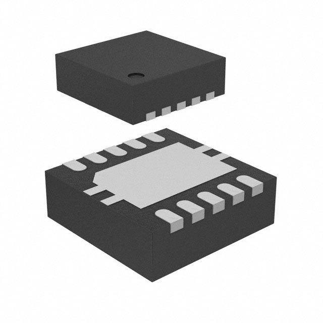
| 供应商器件封装 | 10-SON(3x3) |
| 包装 | 带卷 (TR) |
| 同步整流器 | 是 |
| 商标 | Texas Instruments |
| 安装类型 | 表面贴装 |
| 安装风格 | SMD/SMT |
| 封装 | Reel |
| 封装/外壳 | 10-VFDFN 裸露焊盘 |
| 封装/箱体 | VSON-10 |
| 工作温度 | -40°C ~ 85°C |
| 工作温度范围 | - 40 C to + 85 C |
| 工厂包装数量 | 250 |
| 开关频率 | 2.25 MHz |
| 拓扑结构 | Buck |
| 最大工作温度 | + 85 C |
| 最大输入电压 | 6 V |
| 最小工作温度 | - 40 C |
| 最小输入电压 | 2.5 V |
| 标准包装 | 250 |
| 电压-输入 | 2.5 V ~ 6 V |
| 电压-输出 | 1.2V,1.8V |
| 电流-输出 | 600mA,1A |
| 电源电压-最小 | 2.5 V |
| 类型 | DC/DC Converter |
| 系列 | TPS62421 |
| 输入电压 | 2.5 V to 6 V |
| 输出数 | 2 |
| 输出电压 | 1.2 V, 1.8 V |
| 输出电流 | 600 mA, 1 A |
| 输出端数量 | 2 Output |
| 输出类型 | 固定 |
| 频率-开关 | 2.25MHz |


- 商务部:美国ITC正式对集成电路等产品启动337调查
- 曝三星4nm工艺存在良率问题 高通将骁龙8 Gen1或转产台积电
- 太阳诱电将投资9.5亿元在常州建新厂生产MLCC 预计2023年完工
- 英特尔发布欧洲新工厂建设计划 深化IDM 2.0 战略
- 台积电先进制程称霸业界 有大客户加持明年业绩稳了
- 达到5530亿美元!SIA预计今年全球半导体销售额将创下新高
- 英特尔拟将自动驾驶子公司Mobileye上市 估值或超500亿美元
- 三星加码芯片和SET,合并消费电子和移动部门,撤换高东真等 CEO
- 三星电子宣布重大人事变动 还合并消费电子和移动部门
- 海关总署:前11个月进口集成电路产品价值2.52万亿元 增长14.8%


PDF Datasheet 数据手册内容提取
Product Sample & Technical Tools & Support & Reference Folder Buy Documents Software Community Design TPS62420,TPS62421 SLVS676D–JUNE2006–REVISEDJULY2015 TPS6242x 2.25-MHz 600-mA and 1000-mA Dual Step-Down Converter in Small 3-mm × 3-mm VSON Package 1 Features 3 Description • HighEfficiencyupto95% The TPS6242x device is a synchronous dual step- 1 down DC–DC converter. It provides two independent • V Rangefrom2.5Vto6V IN output voltage rails powered by 1-cell Li-Ion or 3-cell • 2.25-MHzFixedFrequencyOperation NiMH/NiCD batteries. The device is also suitable to • OutputCurrent600mAand1000mA operatefromastandard3.3-Vor5-Vvoltagerail. • AdjustableOutputVoltagefrom0.6VtoV With an input voltage range of 2.5 V to 6 V, the IN • PinSelectableOutputVoltageSupportsSimple TPS6242x is ideal for battery-powered portable applications like smart phones, PDAs, and other DynamicVoltageScaling portableequipment. • OptionalEasyScale™One-PinSerialInterfacefor DynamicOutputVoltageAdjustment With the EasyScale™ serial interface the output voltages can be modified during operation. It • Power-SaveModeatLightLoadCurrents therefore supports dynamic voltage scaling for low • 180° OutofPhaseOperation powerDSPandprocessors. • OutputVoltageAccuracyinPWMMode±1% The TPS6242x operates at 2.25-MHz fixed switching • Typical32-μAQuiescentCurrentforboth frequency and enter the power-save mode operation Converters at light load currents to maintain high efficiency over • 100%DutyCycleforLowestDropout the entire load current range. For low-noise applications the devices can be forced into fixed- • Availableina10-PinVSON(3mm ×3mm) frequency PWM mode by pulling the MODE/DATA pin High. In the shutdown mode, the current 2 Applications consumption is reduced to 1.2 μA. The device allows • CellPhones,Smart-phones theuseofsmallinductorsandcapacitorstoachievea smallsolutionsize. • PDAs,PocketPCs • OMAP™andLowPowerDSPSupply The TPS6242x operates over a free-air temperature range of –40°C to 85°C. It is available in a 10-pin • PortableMediaPlayers leadlesspackage(3mm×3mmVSON) • DigitalRadios • DigitalCameras DeviceInformation(1) PARTNUMBER PACKAGE BODYSIZE(NOM) TPS62420 VSON(10) 3.00mm×3.00mm TPS62421 (1) For all available packages, see the orderable addendum at theendofthedatasheet. TypicalApplicationSchematic EfficiencyvsOutputCurrent TPS62420 100 VIN 2.5V–6V VIN FB 1 L1 V = 1.5V 90 OUT1 10CμINF SW1 2.2μH R11 up to 600mA 80 DEF_1 270kΩ COUT1= 22µF 70 VOUT2= 1.8V VIN= 3.6V R12 60 MODE/DATA= 0 EENN__12 SW2 L2 180kΩ VOUT2= 1.8V Efficiency 4500 VOUT1= 1.5V MDAOTDAE/ ADJ2 2.2μH R36201kΩ 3C3pff2F UCpO tUoT 210=0 202mµAF 2300 R22 GND 180kΩ 10 0 0.01 0.1 1 10 100 1000 IOUTmA 1 An IMPORTANT NOTICE at the end of this data sheet addresses availability, warranty, changes, use in safety-critical applications, intellectualpropertymattersandotherimportantdisclaimers.PRODUCTIONDATA.
TPS62420,TPS62421 SLVS676D–JUNE2006–REVISEDJULY2015 www.ti.com Table of Contents 1 Features.................................................................. 1 8.4 DeviceFunctionalModes........................................11 2 Applications........................................................... 1 8.5 Programming...........................................................13 3 Description............................................................. 1 8.6 RegisterMaps.........................................................17 4 RevisionHistory..................................................... 2 9 ApplicationandImplementation........................ 21 9.1 ApplicationInformation............................................21 5 DeviceComparisonTable..................................... 3 9.2 TypicalApplications................................................22 6 PinConfigurationandFunctions......................... 3 10 PowerSupplyRecommendations..................... 28 7 Specifications......................................................... 4 11 Layout................................................................... 28 7.1 AbsoluteMaximumRatings......................................4 11.1 LayoutGuidelines.................................................28 7.2 ESDRatings..............................................................4 11.2 LayoutExample....................................................28 7.3 RecommendedOperatingConditions.......................4 12 DeviceandDocumentationSupport................. 30 7.4 ThermalInformation..................................................4 7.5 ElectricalCharacteristics...........................................5 12.1 DeviceSupport......................................................30 7.6 DissipationRatings...................................................6 12.2 RelatedLinks........................................................30 7.7 TypicalCharacteristics..............................................7 12.3 CommunityResources..........................................30 12.4 Trademarks...........................................................30 8 DetailedDescription.............................................. 8 12.5 ElectrostaticDischargeCaution............................30 8.1 Overview...................................................................8 12.6 Glossary................................................................30 8.2 FunctionalBlockDiagram.........................................9 13 Mechanical,Packaging,andOrderable 8.3 FeatureDescription.................................................10 Information........................................................... 30 4 Revision History NOTE:Pagenumbersforpreviousrevisionsmaydifferfrompagenumbersinthecurrentversion. ChangesfromRevisionC(June2010)toRevisionD Page • AddedPinConfigurationandFunctionssection,ESDRatingstable,FeatureDescriptionsection,DeviceFunctional Modes,ApplicationandImplementationsection,PowerSupplyRecommendationssection,Layoutsection,Device andDocumentationSupportsection,andMechanical,Packaging,andOrderableInformationsection .............................. 1 2 SubmitDocumentationFeedback Copyright©2006–2015,TexasInstrumentsIncorporated ProductFolderLinks:TPS62420 TPS62421
TPS62420,TPS62421 www.ti.com SLVS676D–JUNE2006–REVISEDJULY2015 5 Device Comparison Table NUPMARBTER OUTPUDTEFVAOULLTTAGE(1) COUURTRPEUNTT PACKAGE(2) ORDERING(3) PMAACRKKAINGGE OUT1 600mA TPS62420 Adjustable TPS62420DRC BQF OUT2 1000mA OUT1:DEF_1=Low 1.2V DRC 600mA TPS62421 OUT1:DEF_1=High 1.8V TPS62421DRC QTQ OUT2 1.8V 1000mA (1) ContactTIforotherfixedoutputvoltageoptions. (2) TheDRC(VSON10PIN)packageisavailableintapeonreel.AddRsuffixtoorderquantitiesof3000partsperreel,Tsuffixfor250 partsperreel. (3) ForthemostcurrentorderinginformationseetheMechanical,Packaging,andOrderableInformationsectionorseetheTIwebsite www.ti.com. 6 Pin Configuration and Functions DRCPackage 10-PinVSON TopView ADJ2 1 10 SW2 MODE/DATA 2 AD 9 EN2 P VIN 3 wer 8 GND o FB1 4 P 7 EN1 DEF_1 5 6 SW1 PinFunctions PIN I/O DESCRIPTION NAME NO. Inputtoadjustoutputvoltageofconverter2.Inadjustableversion(TPS62420)connectanexternal ADJ2 1 I resistordividerbetweenV ,thispinandGNDtosetoutputvoltagebetween0.6VandV .If OUT2 IN EasyScale™interfaceisusedforconverter2,thispinmustbedirectlyconnectedtotheoutput. ThisPinhas2functions: 1. Operationmodeselection:Withlowlevel,power-savemodeisenabledwherethedeviceoperatesin PFM mode at light loads and enters automatically PWM mode at heavy loads. Pulling this PIN to HighforcesthedevicetooperateinPWMmodeoverthewholeloadrange. MODE/DATA 2 I 2. EasyScale™ interface function: One wire serial interface to change the output voltage of both converters.Thepinhasanopen-drainoutputtoprovideanacknowledgeconditionifrequested.The currentintotheopen-drainoutputstagemaynotexceed500μA.TheinterfaceisactiveifeitherEN1 orEN2isHigh. VIN 3 I Supplyvoltage,connecttoVBAT,2.5Vto6V Directfeedbackvoltagesenseinputofconverter1,connectdirectlytoV .Aninternalfeed-forward OUT1 FB1 4 I capacitorisconnectedbetweenthispinandtheerroramplifier.Incaseoffixedoutputvoltageversionsor whentheinterfaceisused,thispinisconnectedtoaninternalresistordividernetwork. Thispindefinestheoutputvoltageofconverter1.ThepinactsinTPS62420asananaloginputforoutput voltagesettingthroughexternalresistors.Infixeddefaultoutputvoltageversionsthispinisadigitalinput DEF_1 5 I/O toselectbetweentwofixeddefaultoutputvoltages,seetableorderinginformation. InTPS62420anexternalresistornetworkneedstobeconnectedtothispintoadjustthedefaultoutput voltage. SW1 6 – Switchpinofconverter1.Connectedtoinductor EN1 7 I Enableinputforconverter1,activehigh GND 8 I GNDforbothconverters,thispinshouldbeconnectedwiththePowerPAD EN2 9 I/O Enableinputforconverter2,activehigh Copyright©2006–2015,TexasInstrumentsIncorporated SubmitDocumentationFeedback 3 ProductFolderLinks:TPS62420 TPS62421
TPS62420,TPS62421 SLVS676D–JUNE2006–REVISEDJULY2015 www.ti.com PinFunctions(continued) PIN I/O DESCRIPTION NAME NO. SW2 10 – Switchpinofconverter2.Connectedtoinductor. PowerPAD™ – – ConnecttoGND 7 Specifications 7.1 Absolute Maximum Ratings Overoperatingfree-airtemperaturerange(unlessotherwisenoted)(1) MIN MAX UNIT InputvoltageonV (2) –0.3 7 V IN VoltageonEN,MODE/DATA,DEF_1 –0.3 V +0.3,≤7 V IN MaximumcurrentintoMODE/DATA 500 μA VoltageonSW1,SW2 –0.3 7 V VoltageonADJ2,FB1 –0.3 V +0.3,≤7 V IN T Maximumjunctiontemperature 150 °C J(max) T Operatingambienttemperature –40 85 °C A T Storagetemperature –65 150 °C stg (1) StressesbeyondthoselistedunderAbsoluteMaximumRatingsmaycausepermanentdamagetothedevice.Thesearestressratings only,andfunctionaloperationofthedeviceattheseoranyotherconditionsbeyondthoseindicatedunderRecommendedOperating Conditionsisnotimplied.Exposuretoabsolute–maximum–ratedconditionsforextendedperiodsmayaffectdevicereliability. (2) Allvoltagevaluesarewithrespecttonetworkgroundterminal. 7.2 ESD Ratings VALUE UNIT Humanbodymodel(HBM),perANSI/ESDA/JEDECJS-001(1) ±2000 V Electrostaticdischarge V (ESD) Charged-devicemodel(CDM),perJEDECspecificationJESD22-C101(2) ±1000 (1) JEDECdocumentJEP155statesthat500-VHBMallowssafemanufacturingwithastandardESDcontrolprocess. (2) JEDECdocumentJEP157statesthat250-VCDMallowssafemanufacturingwithastandardESDcontrolprocess. 7.3 Recommended Operating Conditions Overoperatingfree-airtemperaturerange(unlessotherwisenoted) MIN MAX UNIT V Supplyvoltage 2.5 6 V IN Outputvoltagerangeforadjustablevoltage 0.6 V V IN T Operatingambienttemperature –40 85 °C A T Operatingjunctiontemperature –40 125 °C J 7.4 Thermal Information TPS62420,TPS62421 THERMALMETRIC(1) DRC(VSON) UNIT 10PINS R Junction-to-ambientthermalresistance 45.9 °C/W θJA R Junction-to-case(top)thermalresistance 64.3 °C/W θJC(top) R Junction-to-boardthermalresistance 20.4 °C/W θJB ψ Junction-to-topcharacterizationparameter 1.3 °C/W JT ψ Junction-to-boardcharacterizationparameter 20.6 °C/W JB R Junction-to-case(bottom)thermalresistance 2.8 °C/W θJC(bot) (1) Formoreinformationabouttraditionalandnewthermalmetrics,seetheSemiconductorandICPackageThermalMetricsapplication report,SPRA953. 4 SubmitDocumentationFeedback Copyright©2006–2015,TexasInstrumentsIncorporated ProductFolderLinks:TPS62420 TPS62421
TPS62420,TPS62421 www.ti.com SLVS676D–JUNE2006–REVISEDJULY2015 7.5 Electrical Characteristics V =3.6V,V =1.8V,EN=V ,MODE=GND,L=2.2μH,C =20μF,T =–40°Cto85°CtypicalvaluesareatT = IN OUT IN OUT A A 25°C(unlessotherwisenoted) PARAMETER TESTCONDITIONS MIN TYP MAX UNIT SUPPLYCURRENT V Inputvoltagerange 2.5 6 V IN Oneconverter,I =0mA.PFMmode 19 29 OUT enabled(Mode=0)devicenotswitching, μA EN1=1orEN2=1 Twoconverter,I =0mA.PFMmode 32 48 OUT enabled(Mode=0)devicenotswitching, μA IQ Operatingquiescentcurrent EN1=1andEN2=1 I =0mA,MODE/DATA=GND,forone 23 cOoUnTverter,V 1.575V(1) μA OUT I =0mA,MODE/DATA=V ,forone 3.6 cOoUnTverter,V 1.575V(1) IN mA OUT EN1,EN2=GND,V =3.6V(2) 1.2 3 IN ISD Shutdowncurrent EN1,EN2=GND,VINrampedfrom0Vto 0.1 1 μA 3.6V(3) Falling 1.5 2.35 V Undervoltagelockoutthreshold V UVLO Rising 2.4 ENABLEEN1,EN2 V High-levelinputvoltage,EN1, 1.2 V IH IN V EN2 V Low-levelinputvoltage,EN1, 0 0.4 IL V EN2 I Inputbiascurrent,EN1,EN2 EN1,EN2=GNDorV 0.05 1.0 μA IN IN DEF_1INPUT VDEF_1H DEF_1highlevelinputvoltage DEF_1pinisadigitalinputatfixedoutput 0.9 VIN V V DEF_1lowlevelinputvoltage voltageoptions(TPS62421) 0 0.4 DEF_1L I InputbiasdcurrentDEF_1 DEF_1=GNDorV 0.01 1 μA IN IN MODE/DATA V High-levelinputvoltage, 1.2 V IH IN V MODE/DATA V Low-levelinputvoltage, 0 0.4 IL V MODE/DATA I Inputbiascurrent,MODE/DATA MODE/DATA=GNDorV 0.01 1 μA IN IN V Acknowledgeoutputvoltagehigh Open-drain,throughexternalpullupresistor V V OH IN V Acknowledgeoutputvoltagelow Open-drain,sinkcurrent500μA 0 0.4 V OL INTERFACETIMING t Starttime 2 μs Start t Hightimelowbit,logic0 SignallevelonMODE/DATApinis>1.2V 2 200 H_LB μs detection t Lowtimelowbit,logic0 SignallevelonMODE/DATApin<0.4V 2xt 400 L_LB H_LB μs detection t Lowtimehighbit,logic1 SignallevelonMODE/DATApin<0.4V 2 200 L_HB μs detection t Hightimehighbit,logic1 SignallevelonMODE/DATApinis>1.2V 2xt 400 H_LB L_HS μs detection T EndofStream T 2 μs EOS EOS (1) Deviceisswitchingwithnoloadontheoutput,L=3.3μH,valueincludeslossesofthecoil (2) Thesevaluesarevalidafterthedevicehasbeenalreadyenabledonetime(EN1orEN2=High)andsupplyvoltageV hasnot IN powereddown. (3) Afterthefirstenable,thesevaluesarevalidwhenthedeviceisdisabled(EN1andEN2=Low)andsupplyvoltageV ispoweredup. IN Thevaluesremainvaliduntilthedevicehasbeenenabledfirsttime(EN1orEN2=high). Copyright©2006–2015,TexasInstrumentsIncorporated SubmitDocumentationFeedback 5 ProductFolderLinks:TPS62420 TPS62421
TPS62420,TPS62421 SLVS676D–JUNE2006–REVISEDJULY2015 www.ti.com Electrical Characteristics (continued) V =3.6V,V =1.8V,EN=V ,MODE=GND,L=2.2μH,C =20μF,T =–40°Cto85°CtypicalvaluesareatT = IN OUT IN OUT A A 25°C(unlessotherwisenoted) PARAMETER TESTCONDITIONS MIN TYP MAX UNIT t Durationofacknowledge V 2.5Vto6V 400 520 ACKN IN condition(MODE/DATEline μs pulledlowbythedevice) t Acknowledgevalidtime 2 μs valACK t Time-outforenteringpower-save MODE/DATApinchangesfromhightolow 520 timeout μs mode POWERSWITCH R P-channelMOSFETon- V =V =3.6V 280 620 DS(ON) IN GS mΩ resistance,converter1,2 I P-channelleakagecurrent V =6V 1 μA LK_PMOS DS R N-channelMOSFETon- V =V =3.6V 200 450 DS(ON) IN GS mΩ resistanceconverter1,2 LeakagecurrentintoSW1/SW2 IncludesN-Chanelleakagecurrent, 6 7.5 ILK_SW1/SW2 pin V =open,V =6V,EN=GND(4) μA IN SW OUT1600 0.85 1.0 1.15 Forwardcurrent mA 2.5V≤VIN≤6V I limitPMOSand A LIMF NMOS OUT21000 1.19 1.4 1.61 mA T Thermalshutdown Increasingjunctiontemperature 150 °C SD Thermalshutdownhysteresis Decreasingjunctiontemperature 20 °C OSCILLATOR f Oscillatorfrequency 2.5V≤V ≤6V 2.0 2.25 2.5 MHz SW IN OUTPUT V Adjustableoutputvoltagerange 0.6 V V OUT IN V Referencevoltage 600 mV ref Voltagepositioningactive, V MODE/DATA=GND,deviceoperatingin –1.5% 1.01×V 2.5% OUT(PFM) OUT PFMmode,V =2.5Vto5V (6) (7) DCoutputvoltageaccuracyPFM IN mode,adjustableandfixed MODE/DATA=GND;deviceoperatingin outputvoltage(5) PWMmodeV =2.5Vto6V(7) –1% 0% 1% IN V V =2.5Vto6V,Mode/Data=V ,Fixed OUT PIWNMoperation,0mA<I <I IN (8) –1% 0% 1% OUT OUTMAX DCoutputvoltageloadregulation PWMoperationmode 0.5 %/A t Start-uptime Activationtimetostartswitching(9) 170 μs Startup t V RampUPtime Timetorampfrom5%to95%ofV 750 μs Ramp OUT OUT (4) AtpinsSW1andSW2aninternalresistorof1MΩisconnectedtoGND (5) Outputvoltagespecificationdoesnotincludetoleranceofexternalvoltageprogrammingresistors (6) ConfigurationLtyp2.2μH,C typical20μF,seeparametermeasurementinformation,theoutputvoltagerippledependsonthe OUT effectivecapacitanceoftheoutputcapacitor,largeroutputcapacitorsleadtotighteroutputvoltagetolerance (7) Inpower-savemode,PWMoperationistypicallyenteredatI =V /32Ω. PSM IN (8) ForV >2.2V,V min=V +0.3V OUT IN OUT (9) Thistimeisvalidifoneconverterturnsfromshutdownmode(EN2=0)toactivemode(EN2=1)andtheotherconverterisalready enabled(thatis,EN1=1).Incasebothconvertersareturnedfromshutdownmode(EN1andEN2=Low)toactivemode(EN1and/or EN2=1)avalueoftypical80μsforrampupofinternalcircuitsneedstobeadded.Aftert theconverterstartsswitchingandramps Start V . OUT 7.6 Dissipation Ratings PACKAGE R POWERRATINGFORT ≤25°C DERATINGFACTORABOVET =25°C θJA A A DRC 49°C/W 2050mW 21mW/°C 6 SubmitDocumentationFeedback Copyright©2006–2015,TexasInstrumentsIncorporated ProductFolderLinks:TPS62420 TPS62421
TPS62420,TPS62421 www.ti.com SLVS676D–JUNE2006–REVISEDJULY2015 7.7 Typical Characteristics 2.5 24 2.45 23 2.4 85°C 2.35 22 c - MHz 2.22.53 -40°C dq -Am 21 25°C Fos Id 20 2.2 25°C -40°C 2.15 85°C 19 2.1 18 2.05 2 17 2.5 3 3.5 4 4.5 5 5.5 6 2.5 3 3.5 4 4.5 5 5.5 6 VIN- V VIN- V Figure1.FOSCvsVIN Figure2.IqForOneConverter,NotSwitching 42 0.55 0.5 40 0.45 38 85°C W 0.4 Am 36 n - 85°C Iddq - 34 25°C RDSo 0.35 25°C 0.3 32 -40°C 0.25 -40°C 30 0.2 28 0.15 2.5 3 3.5 4 4.5 5 5.5 6 2.5 3 3.5 4 4.5 5 5.5 6 VIN- V VIN- V Figure3.IqForBothConverters,NotSwitching Figure4.RDSONPMOSvsVIN 0.3 0.25 85°C W 0.2 n - 25°C o S D -40°C R 0.15 0.1 0.05 2.5 3 3.5 4 4.5 5 5.5 6 V - V IN Figure5.R NMOSvsV DSON IN Copyright©2006–2015,TexasInstrumentsIncorporated SubmitDocumentationFeedback 7 ProductFolderLinks:TPS62420 TPS62421
TPS62420,TPS62421 SLVS676D–JUNE2006–REVISEDJULY2015 www.ti.com 8 Detailed Description 8.1 Overview The TPS6242x includes two synchronous step-down converters. The converters operate with typically 2.25-MHz fixed frequency pulse width modulation (PWM) at moderate to heavy load currents. If power-save mode is enabled, the converters automatically enter power-save mode at light load currents and operate in pulse frequency modulation (PFM). During PWM operation the converters use a unique fast response voltage mode controller scheme with input voltage feed-forward to achieve good line and load regulation allowing the use of small ceramic input and output capacitors. At the beginning of each clock cycle initiated by the clock signal, the P-channel MOSFET switch is turned on and the inductor current ramps up until the comparator trips and the controllogicturnsofftheswitch. Each converter integrates two current limits, one in the P-channel MOSFET and another one in the N-channel MOSFET. When the current in the P-channel MOSFET reaches its current limit, the P-channel MOSFET is turned off and the N-channel MOSFET is turned on. If the current in the N-channel MOSFET is above the N- MOS current limit threshold, the N-channel MOSFET remains on until the current drops below its current limit. The two DC/DC converters operate synchronized to each other. A 180° phase shift between converter 1 and converter2decreasestheinputRMScurrent. 8.1.1 Converter1 In the adjustable output voltage version TPS62420 the converter 1 output voltage can be set through an external resistor network on pin DEF_1, which operates as an analog input. In this case, the output voltage can be set in the range of 0.6 V to V . The FB1 pin must be directly connected to the converter 1 output voltage V . It IN OUT1 feedsbacktheoutputvoltagedirectlytotheregulationloop. The output voltage of converter 1 can also be changed by the EasyScale™ serial interface. This makes the deviceveryflexibleforoutputvoltageadjustment.Inthiscase,thedeviceusesaninternalresistornetwork. In the fixed default output voltage version like TPS62421, the DEF_1 pin is configured as a digital input. The converter1defaultsto1.2Vor1.8VdependingonthelevelofDEF_1pin.IfDEF_1islowthedefaultis1.2V;if high, the default is 1.8 V. With the EasyScale™ interface, the output voltage for each DEF_1 pin condition (high orlow)canbechanged. 8.1.2 Converter2 In the adjustable output voltage version TPS62420, the converter 2 output voltage is set by an external resistor dividerconnectedtoADJ2pinandusesanexternalfeed-forwardcapacitorof33pF. In fixed output voltage version TPS62421, the default output voltage is fixed to 1.8 V. In this case, the ADJ2 pin must be connected directly to the converter 2 output voltage V . It is also possible to change the output OUT2 voltage of converter 2 through the EasyScale™ interface. In this case, the ADJ2 pin must be directly connected toconverter2outputvoltageV andnoexternalresistorsmaybeconnected. OUT2 8 SubmitDocumentationFeedback Copyright©2006–2015,TexasInstrumentsIncorporated ProductFolderLinks:TPS62420 TPS62421
TPS62420,TPS62421 www.ti.com SLVS676D–JUNE2006–REVISEDJULY2015 8.2 Functional Block Diagram VIN Converter 1 PMOS Current Limit Comparator VIN FB_VOUT Thermal Shutdown Softstart VREF +1% SkipComp. EN1 FB_VOUT VREF- 1% SkipComp. Low Ext.res.network VREF Control Gate Driver ErrorAmp. Stage DEF1 INnet.t wRoerskistor FVBOUT1 Icnotmerpneanlsated PCWomMp. SW1 C 25pF ff MODE RI 1 Register Sawtooth R DEF1_High Generator GND FB1 RI..N I3 DEF1_Low Average Current Detector NoteA SkipMode Entry NMOS Current Limit Comparator CLK 0° Reference 2.25MHz Load Comparator EasyScale Mode/ Oscillator Interface DATA ACK Undervoltage CLK 180° PMOS Current MOSFET Lockout Limit Comparator Open drain VIN Converter 2 FB_VOUT Int. Resistor VREF +1% Network SkipComp. Register FB_VOUT DEF2 Note B VREF- 1% VREF SkipComp. Low Control Gate Driver Cff25pF ErrorAmp. Stage RI 1 Internal compensated PWM RI..N Comp. SW2 MODE FB_VOUT2 ADJ2 Sawtooth Generator GND Thermal Average Shutdown Current Detector SkipMode Entry NMOS Current Softstart CLK 180° Limit Comparator EN2 Load Comparator GND A. Infixedoutputvoltageversion,thepinDEF_1isconnectedtoaninternaldigitalinputanddisconnectedfromtheerror amplifier B. Tosettheoutputvoltageofconverter2throughEasyScale™interface,ADJ2pinmustbedirectlyconnectedtoV OUT2 Copyright©2006–2015,TexasInstrumentsIncorporated SubmitDocumentationFeedback 9 ProductFolderLinks:TPS62420 TPS62421
TPS62420,TPS62421 SLVS676D–JUNE2006–REVISEDJULY2015 www.ti.com 8.3 Feature Description 8.3.1 DynamicVoltagePositioning This feature reduces the voltage undershoots and overshoots at load steps from light to heavy load and vice versa. It is activated in power-save mode operation. It provides more headroom for both the voltage drop at a loadstep,andthevoltageincreaseataloadthrow-off.Thisimprovesloadtransientbehavior. At light loads, in which the converter operate in PFM mode, the output voltage is regulated typically 1% higher than the nominal value. In case of a load transient from light load to heavy load, the output voltage drops until it reaches the skip comparator low threshold set to –2% below the nominal value and enters PWM mode. During a load throw off from heavy load to light load, the voltage overshoot is also minimized due to active regulation turningontheN-channelswitch. Smooth increased load Fast load transient +1% PFM Mode PFM Mode light load light load V OUT_NOM PWM Mode PWM Mode PWM Mode medium/heavy load medium/heavy load medium/heavy load COMP_LOW threshold –1% Figure6. DynamicVoltagePositioning 8.3.2 UndervoltageLockout The undervoltage lockout circuit prevents the device from malfunctioning at low input voltages and from excessive discharge of the battery and disables the converters. The under-voltage lockout threshold is typically 1.5 V, maximum is 2.35 V. In case the default register values are overwritten by the interface, the new values in the registers REG_DEF_1_Low and REG_DEF_2 remain valid as long the supply voltage does not fall under the undervoltagelockoutthreshold,independentofwhethertheconvertersaredisabled. 8.3.3 ModeSelection The MODE/DATA pin allows mode selection between forced PWM mode and power-save mode for both converters. Furthermore, this pin is a multi-purpose pin and provides (besides mode selection) a one-pin interfacetoreceiveserialdatafromahosttosettheoutputvoltage.ThisisdescribedinthesectionEasyScale™ interface. Connecting this pin to GND enables the automatic PWM and power-save mode operation. The converters operate in fixed-frequency PWM mode at moderate to heavy loads and in the PFM mode during light loads, maintaininghighefficiencyoverawideloadcurrentrange. Pulling the MODE/DATA pin high forces both converters to operate constantly in the PWM mode even at light load currents. The advantage is the converters operate with a fixed frequency that allows simple filtering of the switching frequency for noise sensitive applications. In this mode, the efficiency is lower compared to the power- save mode during light loads. For additional flexibility it is possible to switch from power-save mode to forced PWMmodeduringoperation.Thisallowsefficientpowermanagementbyadjustingtheoperationoftheconverter tothespecificsystemrequirements. In case the operation mode will be changed from forced PWM mode (MODE/DATA = High) to power-save mode Enable (MODE/DATA = 0) the power-save mode will be enabled after a delay time of typically t , which is a timeout maximumof520μs. TheforcedPWMmodeoperationisenabledimmediatelywithpinMODE/DATAsetto1. 10 SubmitDocumentationFeedback Copyright©2006–2015,TexasInstrumentsIncorporated ProductFolderLinks:TPS62420 TPS62421
TPS62420,TPS62421 www.ti.com SLVS676D–JUNE2006–REVISEDJULY2015 Feature Description (continued) 8.3.4 Enable The device has for each converter a separate EN pin to start up each converter independently. If EN1 and EN2 aresettohigh,thecorrespondingconverterstartsupwithsoft-start. Pulling EN1 and EN2 pin low forces the device into shutdown, with a shutdown quiescent current of typically 1.2 μA. In this mode, the P- and N-channel MOSFETs are turned-off and the entire internal control circuitry is switchedoff.ForproperoperationtheEN1andEN2pinsmustbeterminatedandmustnotbeleftfloating. 8.3.5 DEF_1PinFunction The DEF_1 pin is dedicated to converter 1 and makes the output voltage selection very flexible to support dynamicvoltagemanagement.Dependingonthedeviceversion,thispinworkseitheras: 1. Analog input for adjustable output voltage setting (TPS62420): Connecting an external resistor network to this pinadjuststhedefaultoutputvoltagetoanyvaluestartingfrom0.6VtoV . IN 2. Digital input for fixed default output voltage selection (TPS62421): In case this pin is tied to low level, the outputvoltageissetaccordingtothevalueinregisterREG_DEF_1_Low.Thedefaultvoltagewillbe1.2V.Iftied to high level, the output voltage is set according to the value in register REG_DEF_1_High. The default value in this case is 1.8 V. Depending on the level of pin DEF_1, it selects between the two registers REG_DEF_1_Low and REG_DEF_1_High for output voltage setting. Each register content (and therefore output voltage) can be changed individually through the EasyScale™ interface. This makes the device very flexible in terms of output voltagesetting;seeTable4. 8.3.6 180° Out-of-PhaseOperation In PWM mode the converters operate with a 180° turnon phase shift of the PMOS (high side) transistors. It prevents the high-side switches of both converters to be turned on simultaneously, and therefore smooths the inputcurrent.Thisfeaturereducesthesurgecurrentdrawnfromthesupply. 8.3.7 ThermalShutdown As soon as the junction temperature, T , exceeds typically 150°C the device goes into thermal shutdown. In this J mode, the P- and N-channel MOSFETs are turned off. The device continues its operation when the junction temperaturefallsbelowthethermalshutdownhysteresisagain. 8.3.8 ShortCircuitProtection Both outputs are short circuit protected with maximum output current = I (P-MOS and N-MOS). Once the LIMF PMOS switch reaches its current limit, it will be turned off and the NMOS turned on. The PMOS only turns on again,oncethecurrentintheNMOSdecreasesbelowtheNMOScurrentlimit. 8.4 Device Functional Modes 8.4.1 Soft-Start The two converters have an internal soft-start circuit that limits the inrush current during start-up. During soft- start,theoutputvoltagerampupiscontrolledasshowninFigure7. Copyright©2006–2015,TexasInstrumentsIncorporated SubmitDocumentationFeedback 11 ProductFolderLinks:TPS62420 TPS62421
TPS62420,TPS62421 SLVS676D–JUNE2006–REVISEDJULY2015 www.ti.com Device Functional Modes (continued) EN 95% 5% V OUT t t Startup RAMP Figure7. Soft-Start 8.4.2 100%DutyCycleLowDropoutOperation The converters offer a low input to output voltage difference while still maintaining operation with the use of the 100% duty cycle mode. In this mode the P-channel switch is constantly turned on. This is particularly useful in battery-powered applications to achieve longest operation time by taking full advantage of the whole battery voltage range; that is, the minimum input voltage to maintain regulation depends on the load current and output voltage,andcanbecalculatedas: Vinmin(cid:3)Voutmax(cid:2)Ioutmax(cid:1)(cid:4)RDSonmax(cid:2)RL(cid:5) where • Iout =maximumoutputcurrentplusinductorripplecurrent max • RDSon =maximumP-channelswitchRDSon max • R =DCresistanceoftheinductor L • Vout =nominaloutputvoltageplusmaximumoutputvoltagetolerance (1) max With decreasing load current, the device automatically switches into pulse-skipping operation in which the power stage operates intermittently based on load demand. By running cycles periodically the switching losses are minimizedandthedevicerunswithaminimumquiescentcurrentmaintaininghighefficiency. 8.4.3 Power-SaveMode The power-save mode is enabled with MODE/DATA pin set to 0 for both converters. If the load current of a converter decreases, this converter will enter power-save mode operation automatically. The transition to power- save mode of a converter is independent from the operating condition of the other converter. During power-save mode the converter operates with reduced switching frequency in PFM mode and with a minimum quiescent current to maintain high efficiency. The converter will position the output voltage in PFM mode to typically 1.01 × V .Thisvoltagepositioningfeatureminimizesvoltagedropscausedbyasuddenloadstep. OUT To optimize the converter efficiency at light load the average inductor current is monitored. The device changes from PWM mode to power-save mode, if in PWM mode the inductor current falls below a certain threshold. The typical output current threshold depends on V and can be calculated according to Equation 2 for each IN converter. Equation2:AverageoutputcurrentthresholdtoenterPFMmode VIN I (cid:1) DCDC OUT_PFM_enter 32(cid:1) (2) Equation3:AverageoutputcurrentthresholdtoleavePFMmode VIN I (cid:1) DCDC OUT_PFM_leave 24(cid:1) (3) 12 SubmitDocumentationFeedback Copyright©2006–2015,TexasInstrumentsIncorporated ProductFolderLinks:TPS62420 TPS62421
TPS62420,TPS62421 www.ti.com SLVS676D–JUNE2006–REVISEDJULY2015 Device Functional Modes (continued) To keep the output voltage ripple in power-save mode low, the output voltage is monitored with a single threshold comparator (skip comparator). As the output voltage falls below the skip comparator threshold (skip comp) of 1.01 × V , the corresponding converter starts switching for a minimum time period of typically 1 OUTnominal μs and provides current to the load and the output capacitor. Therefore the output voltage increases and the device maintains switching until the output voltage trips the skip comparator threshold (skip comp) again. At this moment all switching activity is stopped and the quiescent current is reduced to minimum. The load is supplied by the output capacitor until the output voltage has dropped below the threshold again. Hereupon the device starts switching again. The power-save mode is exited and PWM mode entered in case the output current exceeds the current IOUT_PFM_leave, or if the output voltage falls below a second comparator threshold, called skip comparator low (skip comp Low) threshold. This skip comparator low threshold is set to –2% below nominal V , and enables a fast transition from power-save mode to PWM mode during a load step. In power-save mode out the quiescent current is reduced typically to 19 μA for one converter and 32 μA for both converters active. This single skip comparator threshold method in power-save mode results in a very low output voltage ripple. The ripple depends on the comparator delay and the size of the output capacitor. Increasing output capacitor values minimizes the output ripple. The power-save mode can be disabled through the MODE/DATA pin set to high. BothconvertersthenoperateinfixedPWMmode.Power-savemodeenable/disableappliestobothconverters. 8.5 Programming 8.5.1 EasyScale™Interface:One-PinSerialInterfaceforDynamicOutputVoltageAdjustment 8.5.1.1 General The EasyScale™ interface is a simple but very flexible one-pin interface to configure the output voltage of both DC–DC converters. The interface is based on a master-slave structure, where the master is typically a micro- controller or application processor. Figure 8 and Table 1 give an overview of the protocol. The protocol consists of a device specific address byte and a data byte. The device specific address byte is fixed to 4E hex. The data byte consists of five bit for information, two address bits and the RFA bit. RFA bit set to high indicates the Request For Acknowledge condition, but the acknowledge condition is only applied if the protocol was received correctly. The advantage of EasyScale™ interface compared to other one-pin interfaces is that its bit detection is, to a large extent, independent from the bit transmission rate. It can automatically detect bit rates from 1.7 kbps to 160 kbps.Furthermore,theinterfaceissharedwiththeMODE/DATApinandrequiresthereforenoadditionalpin. 8.5.1.2 Protocol All bits are transmitted MSB first and LSB last. Figure 9 shows the protocol without acknowledge request (bit RFA=0),Figure10withacknowledge(bitRFA=1)request. Prior to both bytes, device address byte and data byte, a start condition needs to be applied. For this, the MODE/DATA pin needs to be pulled high for at least t before the bit transmission starts with the falling edge. Start In case the MODE/DATA line was already at high level (forced PWM mode selection) no start condition need be appliedpriorthedeviceaddressbyte. Thetransmissionofeachbyteneedstobeclosedwithanend-of-streamconditionforatleastT . EOS 8.5.1.3 BitDecoding The bit detection is based on a PWM scheme, where the criterion is the relation between t and t . It can LOW HIGH besimplifiedto: HighBit:t >t ,butwitht atleast2xt ,seeFigure11 High Low High Low LowBit:t >t ,butwitht atleast2xt ,seeFigure11 Low High Low High The bit detection starts with a falling edge on the MODE/DATA pin and ends with the next falling edge. Dependingontherelationbetweent andt a0or1isdetected. Low High Copyright©2006–2015,TexasInstrumentsIncorporated SubmitDocumentationFeedback 13 ProductFolderLinks:TPS62420 TPS62421
TPS62420,TPS62421 SLVS676D–JUNE2006–REVISEDJULY2015 www.ti.com Programming (continued) 8.5.1.4 Acknowledge Theacknowledgeconditionisonlyappliedif: • acknowledgeisrequestedbyasetRFAbit • thetransmitteddeviceaddressmatcheswiththedeviceaddressofthedevice • 16bitswerereceivedcorrectly In this case, the device turns on the internal ACKN-MOSFET and pulls the MODE/DATA pin low for the time t , which is maximum. 520 μs. The acknowledge condition is valid after an internal delay time t . This ACKN valACK means the internal ACKN-MOSFET is turned on after t , when the last falling edge of the protocol was valACK detected.Themastercontrollerkeepsthelinelowduringthistime. The master device can detect the acknowledge condition with its input by releasing the MODE/DATA pin after t andreadbacka0. valACK In case of an invalid device address or not correctly received protocol, no acknowledge condition will be applied, thus the internal MOSFET will not be turned on and the external pullup resistor pulls MODE/DATA pin high after t .TheMODE/DATApincanbeusedagainaftertheacknowledgeconditionends. valACK NOTE The acknowledge condition may only be requested in case the master device has an open-drainoutput. In case of a push-pull output stage TI recommends to use a series resistor in the MODE/DATA line to limit the currentto500μAincaseofanaccidentallyrequestedacknowledgetoprotecttheinternalACKN-MOSFET. 8.5.1.5 MODESelection Because of the MODE/DATA pin is used for two functions, interface and a mode selection, the device needs to determinewhenithastodecodethebitstreamortochangetheoperationmode. The device enters forced PWM mode operation immediately whenever the MODE/DATA pin turns to high level. ThedevicestaysalsoinforcedPWMmodeduringthewholetimeofaprotocolreception. WithafallingedgeontheMODE/DATApinthedevicestartsbitdecoding.IftheMODE/DATApinstayslowforat leastt ,thedevicegetsaninternaltime-outandpower-savemodeoperationisenabled. timeout Aprotocolwhichissentwithinthistimewillbeignored,becausethefallingedgeforthemodechangewillbefirst interpretedasstartofthefirstbit.Inthiscase,TIrecommendstosendfirsttheprotocolandchangeattheendof theprotocoltopower-savemode. DATAIN DeviceAddress DATABYTE SSttaarrtt DA7 DA6 DA5 DA4 DA3 DA2 DA1 DA0 EOS Start RFA A1 A0 D4 D3 D2 D1 D0 EOS 0 1 0 0 1 1 1 0 DATAOUT ACK Figure8. EasyScale™InterfaceProtocolOverview Table1.EasyScale™InterfaceBitDescription BYTE BIT NAME TRANSMISSION DESCRIPTION NUMBER DIRECTION Device 7 DA7 IN 0MSBdeviceaddress Address 6 DA6 IN 1 Byte 5 DA5 IN 0 4 DA4 IN 0 14 SubmitDocumentationFeedback Copyright©2006–2015,TexasInstrumentsIncorporated ProductFolderLinks:TPS62420 TPS62421
TPS62420,TPS62421 www.ti.com SLVS676D–JUNE2006–REVISEDJULY2015 Programming (continued) Table1.EasyScale™InterfaceBitDescription(continued) BYTE BIT NAME TRANSMISSION DESCRIPTION NUMBER DIRECTION 4Ehex 3 DA3 IN 1 2 DA2 IN 1 1 DA1 IN 1 0 DA0 IN 0LSBdeviceaddress Data 7(MSB) RFA Requestforacknowledge,ifhigh,acknowledgeconditionwillappliedbythedevice Byte 6 A1 Addressbit1 5 A0 Addressbit0 4 D4 Databit4 IN 3 D3 Databit3 2 D2 Databit2 1 D1 Databit1 0(LSB) D0 Databit0 Acknowledgeconditionactive0,thisconditionwillonlybeappliedincaseRFAbitis set.Open-drainoutput,lineneedstobepulledhighbythehostwithapullup ACK OUT resistor. Thisfeaturecanonlybeusedifthemasterhasanopen-drainoutputstage.Incase ofapush-pulloutputstageacknowledgeconditionmaynotberequested! tStart Address Byte tStart DATAByte DATAIN Mode, Static Mode, Static High or Low High or Low DA7 DA0 RFA D0 0 0 T 0 1 T EOS EOS Figure9. EasyScale™InterfaceProtocolWithoutAcknowledge t Address Byte t DATAByte Start Start Mode, Static DATAIN Mode, Static High or Low High or Low DA7 DA0 RFA D0 0 0 T 1 1 t EOS valACK Acknowledge true, Data Line ACKN pulled down by t device Controller needs to ACKN DATAOUT Pullup Data Line via a Acknowledge resistor to detectACKN false, no pull down Figure10. EasyScale™InterfaceProtocolIncludingAcknowledge Copyright©2006–2015,TexasInstrumentsIncorporated SubmitDocumentationFeedback 15 ProductFolderLinks:TPS62420 TPS62421
TPS62420,TPS62421 SLVS676D–JUNE2006–REVISEDJULY2015 www.ti.com t t t t Low High LOW High Low Bit High Bit (Logic 0) (Logic 1) Figure11. EasyScale™Interface – BitCoding MODE/DATA t timeout Power Save Mode Forced PWM MODE Power Save Mode Figure12. MODE/DATAPin:ModeSelection t t Start Address Byte Start DATAByte MODE/DATA T T EOS EOS t timeout Power Save Mode Forced PWM MODE Power Save Mode Figure13. MODE/DATAPin:Power-SaveMode/InterfaceCommunication 16 SubmitDocumentationFeedback Copyright©2006–2015,TexasInstrumentsIncorporated ProductFolderLinks:TPS62420 TPS62421
TPS62420,TPS62421 www.ti.com SLVS676D–JUNE2006–REVISEDJULY2015 8.6 Register Maps Three registers with a data content of 5 bits can be addressed. With 5 bit data content, 32 different values for each register are available. Table 2 shows the addressable registers to set the output voltage when DEF_1 pin works as digital input. In this case, converter 1 has a related register for each DEF_1 pin condition, and one register for converter 2. With a high or low condition on pin DEF_1 (TPS62421) either the content of register REG_DEF_1_High/REG_DEF1_Low is selected. The output voltage of converter 1 is set according to the values in Table 4. Table 3 shows the addressable registers if DEF_1 pin acts as analog input with external resistors connected. In this case one register is available for each converter. The output voltage of converter 1 is set according to the values in Table 5. For converter 2, the available voltages are shown in Table 6. To generate these output voltages a precise internal resistor divider network is used, making external resistors unnecessary (less board space), and provides higher output voltage accuracy. The Interface is activated if at least one of the converters is enabled (EN1 or EN2 is high). After the start-up time t (170 μs) the interface is ready for data Start reception. Table2.AddressableRegistersforFixedOutputVoltageOptions(PinDEF_1=digitalinput) DEVICE REGISTER DESCRIPTION DEF_1 A1 A0 D4 D3 D2 D1 D0 PIN REG_DEF_1_High Converter1outputvoltagesettingfor high 0 1 Outputvoltagesetting,see DEF_1=Highcondition.Thecontentofthe Table4 registerisactivewithDEF1_Pinhigh. REG_DEF_1_Low Converter1outputvoltagesetting low 0 0 Outputvoltagesetting,see TPS62421 Table4 REG_DEF_2 Converter2outputvoltage n/a 1 0 Outputvoltagesetting,see Table6 Donotuse 1 1 Table3.AddressableRegistersforAdjustableOutputVoltageDevices REGISTER DESCRIPTION A1 A0 D4 D3 D2 D1 D0 REG_DEF_1_High NotavailableinTPS62420adjustableversion 0 1 REG_DEF_1_Low Converter1outputvoltagesetting 0 0 TPS62420seeTable5 REG_DEF_2 Converter2outputvoltage 1 0 TPS62420seeTable6,connectADJ2 pindirectlytoV OUT2 Donotuse 1 1 Copyright©2006–2015,TexasInstrumentsIncorporated SubmitDocumentationFeedback 17 ProductFolderLinks:TPS62420 TPS62421
TPS62420,TPS62421 SLVS676D–JUNE2006–REVISEDJULY2015 www.ti.com Table4.SelectableOutputVoltagesforConverter1, WithPinDEF_1asDigitalInput(TPS62421) VOLTAGE[V] VOLTAGE[V] D4 D3 D2 D1 D0 REGISTERREG_DEF_1_LOW REGISTERREG_DEF_1_HIGH 0 0.8 0.9 0 0 0 0 0 1 0.825 0.925 0 0 0 0 1 2 0.85 0.95 0 0 0 1 0 3 0.875 0.975 0 0 0 1 1 4 0.9 1.0 0 0 1 0 0 5 0.925 1.025 0 0 1 0 1 6 0.95 1.050 0 0 1 1 0 7 0.975 1.075 0 0 1 1 1 8 1.0 1.1 0 1 0 0 0 9 1.025 1.125 0 1 0 0 1 10 1.050 1.150 0 1 0 1 0 11 1.075 1.175 0 1 0 1 1 12 1.1 1.2 0 1 1 0 0 13 1.125 1.225 0 1 1 0 1 14 1.150 1.25 0 1 1 1 0 15 1.175 1.275 0 1 1 1 1 16 1.2(defaultTPS62421) 1.3 1 0 0 0 0 17 1.225 1.325 1 0 0 0 1 18 1.25 1.350 1 0 0 1 0 19 1.275 1.375 1 0 0 1 1 20 1.3 1.4 1 0 1 0 0 21 1.325 1.425 1 0 1 0 1 22 1.350 1.450 1 0 1 1 0 23 1.375 1.475 1 0 1 1 1 24 1.4 1.5 1 1 0 0 0 25 1.425 1.525 1 1 0 0 1 26 1.450 1.55 1 1 0 1 0 27 1.475 1.575 1 1 0 1 1 28 1.5 1.6 1 1 1 0 0 29 1.525 1.7 1 1 1 0 1 30 1.55 1.8(defaultTPS62421) 1 1 1 1 0 31 1.575 1.9 1 1 1 1 1 18 SubmitDocumentationFeedback Copyright©2006–2015,TexasInstrumentsIncorporated ProductFolderLinks:TPS62420 TPS62421
TPS62420,TPS62421 www.ti.com SLVS676D–JUNE2006–REVISEDJULY2015 Table5.SelectableOutputVoltagesforConverter1, WithDEF1PinasAnalogInput(TPS62420) TPS62420OUTPUTVOLTAGE[V] D4 D3 D2 D1 D0 REGISTERREG_DEF_1_LOW 0 V AdjustableOutputwithResistorNetworkonDEF_1Pin 0 0 0 0 0 OUT1 0.6VwithDEF_1pinconnectedtoV OUT1 1 0.825 0 0 0 0 1 2 0.85 0 0 0 1 0 3 0.875 0 0 0 1 1 4 0.9 0 0 1 0 0 5 0.925 0 0 1 0 1 6 0.95 0 0 1 1 0 7 0.975 0 0 1 1 1 8 1.0 0 1 0 0 0 9 1.025 0 1 0 0 1 10 1.050 0 1 0 1 0 11 1.075 0 1 0 1 1 12 1.1 0 1 1 0 0 13 1.125 0 1 1 0 1 14 1.150 0 1 1 1 0 15 1.175 0 1 1 1 1 16 1.2 1 0 0 0 0 17 1.225 1 0 0 0 1 18 1.25 1 0 0 1 0 19 1.275 1 0 0 1 1 20 1.3 1 0 1 0 0 21 1.325 1 0 1 0 1 22 1.350 1 0 1 1 0 23 1.375 1 0 1 1 1 24 1.4 1 1 0 0 0 25 1.425 1 1 0 0 1 26 1.450 1 1 0 1 0 27 1.475 1 1 0 1 1 28 1.5 1 1 1 0 0 29 1.525 1 1 1 0 1 30 1.55 1 1 1 1 0 31 1.575 1 1 1 1 1 Copyright©2006–2015,TexasInstrumentsIncorporated SubmitDocumentationFeedback 19 ProductFolderLinks:TPS62420 TPS62421
TPS62420,TPS62421 SLVS676D–JUNE2006–REVISEDJULY2015 www.ti.com Table6.SelectableOutputVoltagesforConverter2, (ADJ2ConnectedtoV ) OUT OUTPUTVOLTAGE[V] D4 D3 D2 D1 D0 FORREGISTERREG_DEF_2 0 V AdjustableOutputwithResistorNetworkonADJ2 0 0 0 0 0 OUT2 (TPS62420) 0.6VwithADJ2pinconnectedtoV (TPS62420) OUT2 1 0.85 0 0 0 0 1 2 0.9 0 0 0 1 0 3 0.95 0 0 0 1 1 4 1.0 0 0 1 0 0 5 1.05 0 0 1 0 1 6 1.1 0 0 1 1 0 7 1.15 0 0 1 1 1 8 1.2 0 1 0 0 0 9 1.25 0 1 0 0 1 10 1.3 0 1 0 1 0 11 1.35 0 1 0 1 1 12 1.4 0 1 1 0 0 13 1.45 0 1 1 0 1 14 1.5 0 1 1 1 0 15 1.55 0 1 1 1 1 16 1.6 1 0 0 0 0 17 1.7 1 0 0 0 1 18 1.8(defaultTPS62421) 1 0 0 1 0 19 1.85 1 0 0 1 1 20 2.0 1 0 1 0 0 21 2.1 1 0 1 0 1 22 2.2 1 0 1 1 0 23 2.3 1 0 1 1 1 24 2.4 1 1 0 0 0 25 2.5 1 1 0 0 1 26 2.6 1 1 0 1 0 27 2.7 1 1 0 1 1 28 2.8 1 1 1 0 0 29 2.85 1 1 1 0 1 30 3.0 1 1 1 1 0 31 3.3 1 1 1 1 1 20 SubmitDocumentationFeedback Copyright©2006–2015,TexasInstrumentsIncorporated ProductFolderLinks:TPS62420 TPS62421
TPS62420,TPS62421 www.ti.com SLVS676D–JUNE2006–REVISEDJULY2015 9 Application and Implementation NOTE Information in the following applications sections is not part of the TI component specification, and TI does not warrant its accuracy or completeness. TI’s customers are responsible for determining suitability of components for their purposes. Customers should validateandtesttheirdesignimplementationtoconfirmsystemfunctionality. 9.1 Application Information 9.1.1 OutputVoltageSetting 9.1.1.1 Converter1AdjustableDefaultOutputVoltageSetting Theoutputvoltagecanbecalculatedto: (cid:4) R (cid:5) 11 VOUT(cid:3)VREF(cid:1) 1(cid:2)R withaninternalreferencevoltageVREFtypical0.6V 12 (4) To keep the operating current to a minimum, TI recommends selecting R within a range of 180 kΩ to 360 kΩ. 12 The sum of R and R should not exceed ~1 MΩ. For higher output voltages than 3.3 V, TI recommends 12 11 choosing lower values than 180 kΩ for R12. Route the DEF_1 line away from noise sources, such as the inductor or the SW1 line. The FB1 line needs to be directly connected to the output capacitor. An internal feed- forward capacitor is connected to this pin, therefore there is no need for an external feed-forward capacitor for converter1. 9.1.1.2 Converter2 The default output voltage of converter 2 can be set by an external resistor network. For converter 2 the same recommendations apply as for converter 1. In addition to that, a 33-pF external feed-forward capacitor C for ff2 goodloadtransientresponsemustbeused. Theoutputvoltagecanbecalculatedto: (cid:4) R (cid:5) 21 VOUT(cid:3)VREF(cid:1) 1(cid:2)R withaninternalreferencevoltageVREFtypical0.6V 22 (5) RoutetheADJ2lineawayfromnoisesources,suchastheinductorortheSW2line.Incasetheinterfaceisused forconverter2,connectADJ2pindirectlytoV OUT2 Copyright©2006–2015,TexasInstrumentsIncorporated SubmitDocumentationFeedback 21 ProductFolderLinks:TPS62420 TPS62421
TPS62420,TPS62421 SLVS676D–JUNE2006–REVISEDJULY2015 www.ti.com 9.2 Typical Applications 9.2.1 TypicalApplicationCircuit1.5-Vand2.85-VAdjustableOutputs TPS62420 VIN 3.3 V–6 V FB 1 VIN L1 V = 1.5 V OUT1 CIN SW1 2.2mH R11 up to 600 mA 10mF 270 kW C = 22mF OUT1 DEF_1 R12 EN_1 180 kW EN_2 L2 V = 2.85 V OUT2 SW2 up to 1000 mA MODE/ 3.3mH R21 Cff2 825 kW 33 pF DATA C = 22mF OUT2 ADJ2 R22 220 kW GND Figure14. TypicalApplicationCircuit1.5-Vand2.85-VAdjustableOutputs 9.2.1.1 DesignRequirements The step-down converter design can be adapted to different output voltage and load current needs by choosing external components appropriate. The following design procedure is adequate for whole V , V and load IN OUT currentrangeofTPS62420. 9.2.1.2 DetailedDesignProcedure 9.2.1.2.1 OutputFilterDesign(InductorandOutputCapacitor) Thedeviceisoptimizedtooperatewithinductorsof2.2μHto4.7 μHandoutputcapacitorsof10 μFto22 μF. Foroperationwitha2.2-μHinductor,a22-μFcapacitorissuggested. 9.2.1.2.1.1 InductorSelection The selected inductor has to be rated for its DC resistance and saturation current. The DC resistance of the inductance will influence directly the efficiency of the converter. Therefore an inductor with lowest DC resistance shouldbeselectedforhighestefficiency. Equation 6 calculates the maximum inductor current under static load conditions. The saturation current of the inductor should be rated higher than the maximum inductor current as calculated with Equation 7. This is recommendedbecauseduringheavyloadtransienttheinductorcurrentwillriseabovethecalculatedvalue. 1(cid:2)Vout (cid:1)I (cid:3)Vout(cid:1) Vin L L(cid:1)ƒ (6) (cid:1)I I (cid:2)I (cid:1) L Lmax outmax 2 where • f=Switchingfrequency(2.25MHztypical) • L=Inductorvalue • ΔI =Peak-to-peakinductorripplecurrent L • I =Maximuminductorcurrent (7) Lmax 22 SubmitDocumentationFeedback Copyright©2006–2015,TexasInstrumentsIncorporated ProductFolderLinks:TPS62420 TPS62421
TPS62420,TPS62421 www.ti.com SLVS676D–JUNE2006–REVISEDJULY2015 Typical Applications (continued) ThehighestinductorcurrentwilloccuratmaximumV . IN Open core inductors have a soft saturation characteristic and they can usually handle higher inductor currents versusacomparableshieldedinductor. A more conservative approach is to select the inductor current rating just for the maximum switch current of the corresponding converter. It must be considered, that the core material from inductor to inductor differs and will haveanimpactontheefficiencyespeciallyathighswitchingfrequencies. RefertoTable7andthetypicalapplicationsforpossibleinductors. Table7.ListofInductors DIMENSIONS[mm3] INDUCTORTYPE SUPPLIER 3.2×2.6×1.0 MIPW3226 FDK 3×3×0.9 LPS3010 Coilcraft 2.8×2.6×1.0 VLF3010 TDK 2.8x2.6×1.4 VLF3014 TDK 3×3×1.4 LPS3015 Coilcraft 3.9×3.9×1.7 LPS4018 Coilcraft 9.2.1.2.1.2 OutputCapacitorSelection The advanced fast response voltage mode control scheme of the two converters allows the use of small ceramic capacitors with a typical value of 10 μF, without having large output voltage undershoots and overshoots during heavy load transients. Ceramic X7R/X5R capacitors having low ESR values result in lowest output voltage ripple andarethereforerecommended. If ceramic output capacitors are used, the capacitor RMS ripple current rating will always meet the application requirements.TheRMSripplecurrentiscalculatedas: Vout 1(cid:2) Vin 1 IRMSCout(cid:3)Vout(cid:1) L(cid:1)ƒ (cid:1)2(cid:1)(cid:4)3 (8) At nominal load current the inductive converters operate in PWM mode and the overall output voltage ripple is the sum of the voltage spike caused by the output capacitor ESR plus the voltage ripple caused by charging and dischargingtheoutputcapacitor: Vout (cid:1)Vout(cid:4)Vout(cid:1)1L(cid:3)(cid:1)Vƒin (cid:1)(cid:5)8(cid:1)Co1ut(cid:1)ƒ(cid:2)ESR(cid:6) (9) WherethehighestoutputvoltagerippleoccursatthehighestinputvoltageV . IN At light load currents the converters operate in power-save mode and the output voltage ripple is dependent on the output capacitor value. The output voltage ripple is set by the internal comparator delay and the external capacitor. Higher output capacitors like 22-μF values minimize the voltage ripple in PFM mode and tighten DC outputaccuracyinPFMmode. 9.2.1.2.1.3 InputCapacitorSelection Because of the nature of the buck converter having a pulsating input current, a low-ESR input capacitor is required for best input voltage filtering and minimizing the interference with other circuits caused by high input voltage spikes. The converters need a ceramic input capacitor of 10 μF. The input capacitor can be increased withoutanylimitforbetterinputvoltagefiltering. Copyright©2006–2015,TexasInstrumentsIncorporated SubmitDocumentationFeedback 23 ProductFolderLinks:TPS62420 TPS62421
TPS62420,TPS62421 SLVS676D–JUNE2006–REVISEDJULY2015 www.ti.com 9.2.1.3 ApplicationCurves 100 100 90 VOUT1= 1.1 V 90 VOUT1= 1.575 V 80 80 70 VIN= 2.7 V VIN= 2.7 V 70 VIN= 2.7 V VIN= 2.7 V Efficiency 456000 VIVNIN= =5 3V.6 V VVIINN== 35. 6V V Efficiency 456000 VIVNIN= =5 3V.6 V VVIINN== 35. 6V V Power Save Mode Forced PWM Mode 30 Power Save Mode 30 MODE/DATA= 0 MODE/DATA= 1 20 MODE/DATA= 0 FMoOrcDeEd/D PAWTAM =M 1ode 20 10 10 0 0 0.01 0.1 1 10 100 1000 0.01 0.1 1 10 100 1000 IOUT- mA IOUT- mA Figure15.EfficiencyVOUT1=1.1V Figure16.EfficiencyVOUT1=1.575V 100 100 VOUT2= 1.8 V VOUT2= 3.3 V 90 90 7800 VIN= 2.7 V VIN= 2.7 V 7800 VIN= 3.6 V VIN= 3.6 V y 60 VIN= 3.6 V VIN= 3.6 V y 60 cienc 50 VIN= 5 V VIN= 5 V cienc 50 VIN= 5 V VIN= 5 V Effi 40 Effi 40 Power Save Mode Forced PWM Mode 30 30 MODE/DATA= 0 MODE/DATA= 1 Power Save Mode Forced PWM Mode MODE/DATA= 0 MODE/DATA= 1 20 20 10 10 0 0 0.01 0.1 1 10 100 1000 0.01 0.1 1 10 100 1000 IOUT- mA IOUT- mA Figure17.EfficiencyV =1.8V Figure18.EfficiencyV =3.3V OUT2 OUT2 100 100 MODE/DATA= 0 IOUT= 100 mA MODE/DATA= 0 95 VOUT= 1.575 V IOUT= 10 mA VOUT= 3.3 V I = 200 mA 90 OUT 90 I = 10 mA 85 OUT cy 80 y 80 IOUT= 1 mA Efficien 7750 IOUT= 1 mA Efficienc 70 65 60 60 55 50 50 2 3 4 5 6 3 4 5 6 VIN- V VIN- V Figure19.EfficiencyvsVIN,VOUT1=1.575V Figure20.EfficiencyvsVIN,VOUT2=3.3V 24 SubmitDocumentationFeedback Copyright©2006–2015,TexasInstrumentsIncorporated ProductFolderLinks:TPS62420 TPS62421
TPS62420,TPS62421 www.ti.com SLVS676D–JUNE2006–REVISEDJULY2015 1.650 3.4 VOUT1= 1.575 V VOUT2= 3.3 V MODE/DATA= low, PFM Mode, voltage positioning active 1.625 MODE/DATA= low, PFM Mode, voltage positioning active VIN= 5 V VIN= 4.2 V PWM Mode 3.35 PWM Mode Operation Operation DC - V 1.600 VIN= 2.7 V VIN= 3.6 V C - V VIN= 3.7 V VIN= 4.2 V T 1.575 D 3.3 VOU VIN= 2.7 V VIN= 3.6 V VIN= 4.2 V VOUT VIMNO=D 3E./7D AVTA=V hIiNgh=, f4o.r2c eVd PWVMIN M=o d5e V 1.550 MODE/DATA= high, forced PWM Mode 3.25 1.525 1.500 3.2 0.01 0.10 1 10 100 1000 0.01 0.10 1 10 100 1000 IOUT- mA IOUT- mA Figure21.DCOutputAccuracyVOUT1=1.575V Figure22.DCOutputAccuracyVOUT2=3.3V Power Save Mode Mode/Data = high, Mode/Data = low IOUT= 10mA forced PWM MODE operation IOUT= 10mA VOUT= 1.8V 20mV/Div VOUT= 1.8V 20mV/Div Inductor current 100mA/Div Inductor current 100mA/Div Time base - 10ms/Div Time base - 400 ns/Div Figure23.LightLoadOutputVoltageRipple Figure24.OutputVoltageRippleinForcedPWMMode inPower-SaveMode PWM MODE OPERATION VOUT= 1.8V Forced PWM MODE/DATA1V/Div IOUT= 400mA Mode VOUT ripple 20mV/Div Enable Power Save Mode Entering PFM Mode Voltage positioning active VOUT 20mV/Div Inductor current 200mA/Div VOUT= 1.8V IOUT= 20mA Time base - 200 ns/Div Time base - 20ms/Div Figure25.OutputVoltageRipple Figure26.ForcedPWM/PFMModeTransition inPWMMode Copyright©2006–2015,TexasInstrumentsIncorporated SubmitDocumentationFeedback 25 ProductFolderLinks:TPS62420 TPS62421
TPS62420,TPS62421 SLVS676D–JUNE2006–REVISEDJULY2015 www.ti.com VOUT= 1.575V MODE/DATA= high VOUT= 1.575V MODE/DATA= low 50mV/Div PWM Mode operation 50mV/Div Voltage positioningin PFM Mode reducesvoltagedrop PWM Mode operation during load step IOUT1 = 540mA IOUT200mA/Div IOUT1 = 540mA IOUT200mA/Div IOUT= 60mA IOUT= 60mA Time base - 100ms/Div Time base - 100ms/Div Figure27.LoadTransientResponsePFM/PWM Figure28.LoadTransientResponsePWMOperation VIN 3.6V to 4.6V MODE/DATA= high EN1 / EN2 5V/Div VIN 1V/Div VIN = 3.8V IOUT1 max = 400mA VOUT1 500mV/Div VOUT1.575 IOUT200mA SW1 1V/Div VOUT50mV/Div Icoil 500mA/Div Time base - 400ms/Div Time base - 200ms/Div Figure29.LineTransientResponse Figure30.Start-UpTimingOneConverter SW1 5V/Div SW1 5V/Div I 200mA/Div I 200mA/Div coil1 coil1 SW2 5V/Div SW2 5V/Div Icoil2200mA/Div Icoil2200mA/Div VIN3.6V, VIN3.6V, VOUT1: 1.575V VOUT1: 1.8V VIOOUUTT12=: 1IO.8UVT2= 200mA VIOOUUTT12=: 3IO.0UVT2= 200mA Time base - 100 ns/Div Time base - 100 ns/Div Figure31.TypicalOperationVIN=3.6V, Figure32.TypicalOperationVIN=3.6V, VOUT1=1.575V,VOUT2=1.8V VOUT1=1.8V,VOUT2=3V 26 SubmitDocumentationFeedback Copyright©2006–2015,TexasInstrumentsIncorporated ProductFolderLinks:TPS62420 TPS62421
TPS62420,TPS62421 www.ti.com SLVS676D–JUNE2006–REVISEDJULY2015 SW1 5V/Div MODE/DATA 2V/Div I 200mA/Div coil1 SW2 5V/Div VOUT1: 200mV/Div VOUT1: 1.5V V 3.8V IN ACKN = off I = 150mA OUT1 Icoil2200mA/Div VVIN3.6: V1.,2V VOUT1: 1.1V REG_DEF_1_Low OUT1 V : 1.2V OUT2 I = I = 200mA OUT1 OUT2 Time base - 100 ns/Div Time base - 100ms/Div Figure33.TypicalOperationVIN=3.6V, Figure34.VOUT1ChangeWithEasyScale™Interface V =1.2V,V =1.2V OUT1 OUT2 9.2.2 TypicalApplicationCircuitTPS62421 In fixed output voltage version TPS62421, the default output voltage of converter 1 is fixed to 1.2 V or 1.8 V dependingontheDEF_1pinlevel.Thedefaultoutputvoltageofconverter2isfixedto1.8V.TheADJ2pinmust beconnecteddirectlytotheconverter2outputvoltage. TPS62421 VIN 2.5 V–6 V VIN FB 1 2.2mH V = 1.2V / 1.8V OUT1 10mF SW1 600 mA 1.8V DEF_1 1.2V 22mF EN_1 EN_2 2.2mH V = 1.8 V OUT2 SW2 1000 mA MODE/ 22mF DATA ADJ2 GND Figure35. TypicalApplicationCircuitTPS62421 Copyright©2006–2015,TexasInstrumentsIncorporated SubmitDocumentationFeedback 27 ProductFolderLinks:TPS62420 TPS62421
TPS62420,TPS62421 SLVS676D–JUNE2006–REVISEDJULY2015 www.ti.com 10 Power Supply Recommendations The TPS6242x device has no special requirements for its input power supply. The input power supply's output currentneedstoberatedaccordingtothesupplyvoltage,outputvoltageandoutputcurrentoftheTPS6242x. 11 Layout 11.1 Layout Guidelines As for all switching power supplies, the layout is an important step in the design. Proper function of the device demands careful attention to PCB layout. Take care in board layout to get the specified performance. If the layout is not carefully done, the regulator could show poor line and/or load regulation, stability issues as well as EMI problems. It is critical to provide a low inductance, impedance ground path. Therefore, use wide and short tracesforthemaincurrentpathsasindicatedinboldinFigure36. The input capacitor should be placed as close as possible to the IC pins as well as the inductor and output capacitor. Connect the GND pin of the device to the PowerPAD of the PCB and use this pad as a star point. For each converter use a common power GND node and a different node for the signal GND to minimize the effects of ground noise. Connect these ground nodes together to the PowerPAD (star point) underneath the IC. Keep the common path to the GND pin, which returns the small signal components and the high current of the output capacitors as short as possible to avoid ground noise. The output voltage sense lines (FB1, ADJ2, DEF_1) should be connected right to the output capacitor and routed away from noisy components and traces (that is, SW line). If the EasyScale™ interface is operated with high transmission rates, the MODE/DATA trace must be routed away from the ADJ2 line to avoid capacitive coupling into the ADJ2 pin. A GND guard ring between the MODE/DATApinandADJ2pinavoidspotentialnoisecoupling. 11.2 Layout Example TPS62420 VIN 2.5 V– 6 V VIN EN_1 C IN EN_2 10mF MODE/ DATA FB 1 L2 L1 SW2 SW1 C 3.3mH 3.3mH ff2 33 pF R21 R11 COUT2 COUT2 ADJ2 DEF_1 R22 R12 PowerPAD GND Figure36. LayoutDiagram 28 SubmitDocumentationFeedback Copyright©2006–2015,TexasInstrumentsIncorporated ProductFolderLinks:TPS62420 TPS62421
TPS62420,TPS62421 www.ti.com SLVS676D–JUNE2006–REVISEDJULY2015 Layout Example (continued) C OUT1 C IN GND Pin connected with Power Pad C OUT2 Figure37. PCBLayout Copyright©2006–2015,TexasInstrumentsIncorporated SubmitDocumentationFeedback 29 ProductFolderLinks:TPS62420 TPS62421
TPS62420,TPS62421 SLVS676D–JUNE2006–REVISEDJULY2015 www.ti.com 12 Device and Documentation Support 12.1 Device Support 12.1.1 Third-PartyProductsDisclaimer TI'S PUBLICATION OF INFORMATION REGARDING THIRD-PARTY PRODUCTS OR SERVICES DOES NOT CONSTITUTE AN ENDORSEMENT REGARDING THE SUITABILITY OF SUCH PRODUCTS OR SERVICES OR A WARRANTY, REPRESENTATION OR ENDORSEMENT OF SUCH PRODUCTS OR SERVICES, EITHER ALONEORINCOMBINATIONWITHANYTIPRODUCTORSERVICE. 12.2 Related Links The table below lists quick access links. Categories include technical documents, support and community resources,toolsandsoftware,andquickaccesstosampleorbuy. Table8.RelatedLinks TECHNICAL TOOLS& SUPPORT& PARTS PRODUCTFOLDER SAMPLE&BUY DOCUMENTS SOFTWARE COMMUNITY TPS62420 Clickhere Clickhere Clickhere Clickhere Clickhere TPS62421 Clickhere Clickhere Clickhere Clickhere Clickhere 12.3 Community Resources The following links connect to TI community resources. Linked contents are provided "AS IS" by the respective contributors. They do not constitute TI specifications and do not necessarily reflect TI's views; see TI's Terms of Use. TIE2E™OnlineCommunity TI'sEngineer-to-Engineer(E2E)Community.Createdtofostercollaboration amongengineers.Ate2e.ti.com,youcanaskquestions,shareknowledge,exploreideasandhelp solveproblemswithfellowengineers. DesignSupport TI'sDesignSupport QuicklyfindhelpfulE2Eforumsalongwithdesignsupporttoolsand contactinformationfortechnicalsupport. 12.4 Trademarks EasyScale,OMAP,PowerPAD,E2EaretrademarksofTexasInstruments. Allothertrademarksarethepropertyoftheirrespectiveowners. 12.5 Electrostatic Discharge Caution Thesedeviceshavelimitedbuilt-inESDprotection.Theleadsshouldbeshortedtogetherorthedeviceplacedinconductivefoam duringstorageorhandlingtopreventelectrostaticdamagetotheMOSgates. 12.6 Glossary SLYZ022—TIGlossary. Thisglossarylistsandexplainsterms,acronyms,anddefinitions. 13 Mechanical, Packaging, and Orderable Information The following pages include mechanical, packaging, and orderable information. This information is the most current data available for the designated devices. This data is subject to change without notice and revision of thisdocument.Forbrowser-basedversionsofthisdatasheet,refertotheleft-handnavigation. 30 SubmitDocumentationFeedback Copyright©2006–2015,TexasInstrumentsIncorporated ProductFolderLinks:TPS62420 TPS62421
PACKAGE OPTION ADDENDUM www.ti.com 6-Feb-2020 PACKAGING INFORMATION Orderable Device Status Package Type Package Pins Package Eco Plan Lead/Ball Finish MSL Peak Temp Op Temp (°C) Device Marking Samples (1) Drawing Qty (2) (6) (3) (4/5) TPS62420DRCR ACTIVE VSON DRC 10 3000 Green (RoHS NIPDAU Level-2-260C-1 YEAR -40 to 85 BQF & no Sb/Br) TPS62420DRCRG4 ACTIVE VSON DRC 10 3000 Green (RoHS NIPDAU Level-2-260C-1 YEAR -40 to 85 BQF & no Sb/Br) TPS62420DRCT ACTIVE VSON DRC 10 250 Green (RoHS NIPDAU Level-2-260C-1 YEAR -40 to 85 BQF & no Sb/Br) TPS62420DRCTG4 ACTIVE VSON DRC 10 250 Green (RoHS NIPDAU Level-2-260C-1 YEAR -40 to 85 BQF & no Sb/Br) TPS62421DRCR ACTIVE VSON DRC 10 3000 Green (RoHS NIPDAU Level-2-260C-1 YEAR -40 to 85 QTQ & no Sb/Br) TPS62421DRCT ACTIVE VSON DRC 10 250 Green (RoHS NIPDAU Level-2-260C-1 YEAR -40 to 85 QTQ & no Sb/Br) (1) The marketing status values are defined as follows: ACTIVE: Product device recommended for new designs. LIFEBUY: TI has announced that the device will be discontinued, and a lifetime-buy period is in effect. NRND: Not recommended for new designs. Device is in production to support existing customers, but TI does not recommend using this part in a new design. PREVIEW: Device has been announced but is not in production. Samples may or may not be available. OBSOLETE: TI has discontinued the production of the device. (2) RoHS: TI defines "RoHS" to mean semiconductor products that are compliant with the current EU RoHS requirements for all 10 RoHS substances, including the requirement that RoHS substance do not exceed 0.1% by weight in homogeneous materials. Where designed to be soldered at high temperatures, "RoHS" products are suitable for use in specified lead-free processes. TI may reference these types of products as "Pb-Free". RoHS Exempt: TI defines "RoHS Exempt" to mean products that contain lead but are compliant with EU RoHS pursuant to a specific EU RoHS exemption. Green: TI defines "Green" to mean the content of Chlorine (Cl) and Bromine (Br) based flame retardants meet JS709B low halogen requirements of <=1000ppm threshold. Antimony trioxide based flame retardants must also meet the <=1000ppm threshold requirement. (3) MSL, Peak Temp. - The Moisture Sensitivity Level rating according to the JEDEC industry standard classifications, and peak solder temperature. (4) There may be additional marking, which relates to the logo, the lot trace code information, or the environmental category on the device. (5) Multiple Device Markings will be inside parentheses. Only one Device Marking contained in parentheses and separated by a "~" will appear on a device. If a line is indented then it is a continuation of the previous line and the two combined represent the entire Device Marking for that device. Addendum-Page 1
PACKAGE OPTION ADDENDUM www.ti.com 6-Feb-2020 (6) Lead/Ball Finish - Orderable Devices may have multiple material finish options. Finish options are separated by a vertical ruled line. Lead/Ball Finish values may wrap to two lines if the finish value exceeds the maximum column width. Important Information and Disclaimer:The information provided on this page represents TI's knowledge and belief as of the date that it is provided. TI bases its knowledge and belief on information provided by third parties, and makes no representation or warranty as to the accuracy of such information. Efforts are underway to better integrate information from third parties. TI has taken and continues to take reasonable steps to provide representative and accurate information but may not have conducted destructive testing or chemical analysis on incoming materials and chemicals. TI and TI suppliers consider certain information to be proprietary, and thus CAS numbers and other limited information may not be available for release. In no event shall TI's liability arising out of such information exceed the total purchase price of the TI part(s) at issue in this document sold by TI to Customer on an annual basis. OTHER QUALIFIED VERSIONS OF TPS62420 : •Automotive: TPS62420-Q1 NOTE: Qualified Version Definitions: •Automotive - Q100 devices qualified for high-reliability automotive applications targeting zero defects Addendum-Page 2
PACKAGE MATERIALS INFORMATION www.ti.com 4-Mar-2015 TAPE AND REEL INFORMATION *Alldimensionsarenominal Device Package Package Pins SPQ Reel Reel A0 B0 K0 P1 W Pin1 Type Drawing Diameter Width (mm) (mm) (mm) (mm) (mm) Quadrant (mm) W1(mm) TPS62420DRCR VSON DRC 10 3000 330.0 12.4 3.3 3.3 1.1 8.0 12.0 Q2 TPS62420DRCR VSON DRC 10 3000 330.0 12.4 3.3 3.3 1.1 8.0 12.0 Q2 TPS62420DRCT VSON DRC 10 250 180.0 12.4 3.3 3.3 1.1 8.0 12.0 Q2 TPS62420DRCT VSON DRC 10 250 180.0 12.4 3.3 3.3 1.1 8.0 12.0 Q2 TPS62421DRCR VSON DRC 10 3000 330.0 12.4 3.3 3.3 1.1 8.0 12.0 Q2 TPS62421DRCT VSON DRC 10 250 180.0 12.4 3.3 3.3 1.1 8.0 12.0 Q2 PackMaterials-Page1
PACKAGE MATERIALS INFORMATION www.ti.com 4-Mar-2015 *Alldimensionsarenominal Device PackageType PackageDrawing Pins SPQ Length(mm) Width(mm) Height(mm) TPS62420DRCR VSON DRC 10 3000 367.0 367.0 35.0 TPS62420DRCR VSON DRC 10 3000 367.0 367.0 35.0 TPS62420DRCT VSON DRC 10 250 210.0 185.0 35.0 TPS62420DRCT VSON DRC 10 250 210.0 185.0 35.0 TPS62421DRCR VSON DRC 10 3000 367.0 367.0 35.0 TPS62421DRCT VSON DRC 10 250 210.0 185.0 35.0 PackMaterials-Page2
GENERIC PACKAGE VIEW DRC 10 VSON - 1 mm max height PLASTIC SMALL OUTLINE - NO LEAD Images above are just a representation of the package family, actual package may vary. Refer to the product data sheet for package details. 4204102-3/M
PACKAGE OUTLINE DRC0010J VSON - 1 mm max height SCALE 4.000 PLASTIC SMALL OUTLINE - NO LEAD 3.1 B A 2.9 PIN 1 INDEX AREA 3.1 2.9 1.0 C 0.8 SEATING PLANE 0.05 0.00 0.08 C 1.65 0.1 2X (0.5) (0.2) TYP EXPOSED 4X (0.25) THERMAL PAD 5 6 2X 11 SYMM 2 2.4 0.1 10 1 8X 0.5 0.30 10X 0.18 PIN 1 ID SYMM 0.1 C A B (OPTIONAL) 0.5 0.05 C 10X 0.3 4218878/B 07/2018 NOTES: 1. All linear dimensions are in millimeters. Any dimensions in parenthesis are for reference only. Dimensioning and tolerancing per ASME Y14.5M. 2. This drawing is subject to change without notice. 3. The package thermal pad must be soldered to the printed circuit board for optimal thermal and mechanical performance. www.ti.com
EXAMPLE BOARD LAYOUT DRC0010J VSON - 1 mm max height PLASTIC SMALL OUTLINE - NO LEAD (1.65) (0.5) 10X (0.6) 1 10 10X (0.24) 11 SYMM (2.4) (3.4) (0.95) 8X (0.5) 6 5 (R0.05) TYP ( 0.2) VIA TYP (0.25) (0.575) SYMM (2.8) LAND PATTERN EXAMPLE EXPOSED METAL SHOWN SCALE:20X 0.07 MIN 0.07 MAX EXPOSED METAL ALL AROUND ALL AROUND EXPOSED METAL SOLDER MASK METAL METAL UNDER SOLDER MASK OPENING SOLDER MASK OPENING NON SOLDER MASK SOLDER MASK DEFINED DEFINED (PREFERRED) SOLDER MASK DETAILS 4218878/B 07/2018 NOTES: (continued) 4. This package is designed to be soldered to a thermal pad on the board. For more information, see Texas Instruments literature number SLUA271 (www.ti.com/lit/slua271). 5. Vias are optional depending on application, refer to device data sheet. If any vias are implemented, refer to their locations shown on this view. It is recommended that vias under paste be filled, plugged or tented. www.ti.com
EXAMPLE STENCIL DESIGN DRC0010J VSON - 1 mm max height PLASTIC SMALL OUTLINE - NO LEAD 2X (1.5) (0.5) SYMM EXPOSED METAL 11 TYP 10X (0.6) 1 10 (1.53) 10X (0.24) 2X (1.06) SYMM (0.63) 8X (0.5) 6 5 (R0.05) TYP 4X (0.34) 4X (0.25) (2.8) SOLDER PASTE EXAMPLE BASED ON 0.125 mm THICK STENCIL EXPOSED PAD 11: 80% PRINTED SOLDER COVERAGE BY AREA SCALE:25X 4218878/B 07/2018 NOTES: (continued) 6. Laser cutting apertures with trapezoidal walls and rounded corners may offer better paste release. IPC-7525 may have alternate design recommendations. www.ti.com
IMPORTANTNOTICEANDDISCLAIMER TI PROVIDES TECHNICAL AND RELIABILITY DATA (INCLUDING DATASHEETS), DESIGN RESOURCES (INCLUDING REFERENCE DESIGNS), APPLICATION OR OTHER DESIGN ADVICE, WEB TOOLS, SAFETY INFORMATION, AND OTHER RESOURCES “AS IS” AND WITH ALL FAULTS, AND DISCLAIMS ALL WARRANTIES, EXPRESS AND IMPLIED, INCLUDING WITHOUT LIMITATION ANY IMPLIED WARRANTIES OF MERCHANTABILITY, FITNESS FOR A PARTICULAR PURPOSE OR NON-INFRINGEMENT OF THIRD PARTY INTELLECTUAL PROPERTY RIGHTS. These resources are intended for skilled developers designing with TI products. You are solely responsible for (1) selecting the appropriate TI products for your application, (2) designing, validating and testing your application, and (3) ensuring your application meets applicable standards, and any other safety, security, or other requirements. These resources are subject to change without notice. TI grants you permission to use these resources only for development of an application that uses the TI products described in the resource. Other reproduction and display of these resources is prohibited. No license is granted to any other TI intellectual property right or to any third party intellectual property right. TI disclaims responsibility for, and you will fully indemnify TI and its representatives against, any claims, damages, costs, losses, and liabilities arising out of your use of these resources. TI’s products are provided subject to TI’s Terms of Sale (www.ti.com/legal/termsofsale.html) or other applicable terms available either on ti.com or provided in conjunction with such TI products. TI’s provision of these resources does not expand or otherwise alter TI’s applicable warranties or warranty disclaimers for TI products. Mailing Address: Texas Instruments, Post Office Box 655303, Dallas, Texas 75265 Copyright © 2020, Texas Instruments Incorporated