ICGOO在线商城 > TPS57160QDRCRQ1
 Datasheet下载
- 型号: TPS57160QDRCRQ1
- 制造商: Texas Instruments
- 库位|库存: xxxx|xxxx
- 要求:
| 数量阶梯 | 香港交货 | 国内含税 |
| +xxxx | $xxxx | ¥xxxx |
查看当月历史价格
查看今年历史价格
TPS57160QDRCRQ1产品简介:
ICGOO电子元器件商城为您提供TPS57160QDRCRQ1由Texas Instruments设计生产,在icgoo商城现货销售,并且可以通过原厂、代理商等渠道进行代购。 提供TPS57160QDRCRQ1价格参考以及Texas InstrumentsTPS57160QDRCRQ1封装/规格参数等产品信息。 你可以下载TPS57160QDRCRQ1参考资料、Datasheet数据手册功能说明书, 资料中有TPS57160QDRCRQ1详细功能的应用电路图电压和使用方法及教程。
| 参数 | 数值 |
| 产品目录 | 集成电路 (IC) |
| 描述 | IC REG BUCK ADJ 1.5A 10SON |
| 产品分类 | |
| 品牌 | Texas Instruments |
| 数据手册 | |
| 产品图片 |
|
| 产品型号 | TPS57160QDRCRQ1 |
| PWM类型 | 电流模式 |
| rohs | 无铅 / 符合限制有害物质指令(RoHS)规范要求 |
| 产品系列 | Automotive, AEC-Q100, SWIFT™, Eco-Mode™ |
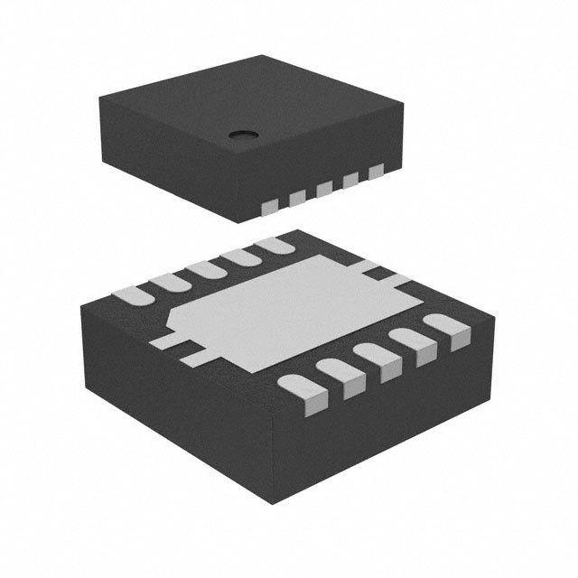
| 供应商器件封装 | 10-SON(3x3) |
| 其它名称 | 296-28175-6 |
| 制造商产品页 | http://www.ti.com/general/docs/suppproductinfo.tsp?distId=10&orderablePartNumber=TPS57160QDRCRQ1 |
| 包装 | Digi-Reel® |
| 同步整流器 | 无 |
| 安装类型 | 表面贴装 |
| 封装/外壳 | 10-VFDFN 裸露焊盘 |
| 工作温度 | -40°C ~ 150°C |
| 标准包装 | 1 |
| 电压-输入 | 3.5 V ~ 60 V |
| 电压-输出 | 0.8 V ~ 58 V |
| 电流-输出 | 1.5A |
| 类型 | 降压(降压) |
| 设计资源 | http://www.digikey.com/product-highlights/cn/zh/texas-instruments-webench-design-center/3176 |
| 输出数 | 1 |
| 输出类型 | 可调式 |
| 频率-开关 | 100kHz ~ 2.5MHz |


- 商务部:美国ITC正式对集成电路等产品启动337调查
- 曝三星4nm工艺存在良率问题 高通将骁龙8 Gen1或转产台积电
- 太阳诱电将投资9.5亿元在常州建新厂生产MLCC 预计2023年完工
- 英特尔发布欧洲新工厂建设计划 深化IDM 2.0 战略
- 台积电先进制程称霸业界 有大客户加持明年业绩稳了
- 达到5530亿美元!SIA预计今年全球半导体销售额将创下新高
- 英特尔拟将自动驾驶子公司Mobileye上市 估值或超500亿美元
- 三星加码芯片和SET,合并消费电子和移动部门,撤换高东真等 CEO
- 三星电子宣布重大人事变动 还合并消费电子和移动部门
- 海关总署:前11个月进口集成电路产品价值2.52万亿元 增长14.8%


PDF Datasheet 数据手册内容提取
Product Sample & Technical Tools & Support & Folder Buy Documents Software Community TPS57160-Q1 SLVSAP1E–DECEMBER2010–REVISEDMARCH2015 TPS57160-Q1 1.5-A 60-V Step-Down DC-DC Converter With Eco-mode™ Control 1 Features 3 Description • QualifiedforAutomotiveApplications The TPS57160-Q1 device is a 60-V 1.5-A step-down 1 regulator with an integrated high-side MOSFET. • 3.5-Vto60-VInputVoltageRange Current-mode control provides simple external • 200-mΩ High-SideMOSFET compensation and flexible component selection. A • HighEfficiencyatLightLoadsWithPulse- low-ripple pulse-skip mode reduces the no load, input SkippingEco-mode™ControlScheme supply current to 116 μA. Using the enable pin, shutdownsupplycurrentisreducedto1.5 μA. • 116-μAOperatingQuiescentCurrent Undervoltage lockout is set internally at 2.5 V but can • 1.5-μAShutdownCurrent beincreasedusingtheenablepin.Theoutputvoltage • 100-kHzto2.5-MHzSwitchingFrequency startup ramp is controlled by the slow-start pin that • SynchronizestoExternalClock can also be configured for sequencing or tracking. An • AdjustableSlowStart/Sequencing open-drain power-good signal indicates the output is within92%to109%ofthenominalvoltage. • UndervoltageandOvervoltagePower-good Output A wide switching frequency range allows efficiency and external component size to be optimized. • AdjustableUndervoltageLockout(UVLO)Voltage Frequency foldback and thermal shutdown protects andHysteresis thepartduringanoverloadcondition. • 0.8-VInternalVoltageReference The TPS57160-Q1 device is available in a 10-pin • Supportedby SwitcherPro™SoftwareTool thermally enhanced MSOP-PowerPAD™ (DGQ) or (ti.com/tool/switcherpro) 10-pin VSON (DRC) package. The Z-suffix offers • Z-SuffixOffersImprovedDelamination reduceddelaminationcomparedtostandarddevice. 2 Applications DeviceInformation(1) • 12-V,24-V,and48-VIndustrialandCommercial PARTNUMBER PACKAGE BODYSIZE(NOM) Low-PowerSystems MSOP-PowerPAD(10) 3.00mm×3.00mm TPS57160-Q1 • AftermarketAutomotiveAccessories:Video,GPS, VSON(10) 3.00mm×3.00mm Entertainment (1) For all available packages, see the orderable addendum at theendofthedatasheet. 4 Simplified Schematic EFFICIENCY VIN PWRGD vs LOAD CURRENT TPS57160 90 85 EN BOOT 80 PH y - % 75 nc 70 SS/TR cie RT/CLK Effi 65 COMP 60 VI= 12 V, VSENSE V = 3.3 V, O 55 fsw= 1200 kHz 50 GND 0 0.25 0.50 0.75 1 1.25 1.50 1.75 2 Load Current -A 1 An IMPORTANT NOTICE at the end of this data sheet addresses availability, warranty, changes, use in safety-critical applications, intellectualpropertymattersandotherimportantdisclaimers.PRODUCTIONDATA.
TPS57160-Q1 SLVSAP1E–DECEMBER2010–REVISEDMARCH2015 www.ti.com Table of Contents 1 Features.................................................................. 1 8.3 FeatureDescription.................................................12 2 Applications........................................................... 1 8.4 DeviceFunctionalModes........................................24 3 Description............................................................. 1 9 ApplicationandImplementation........................ 29 4 SimplifiedSchematic............................................. 1 9.1 ApplicationInformation............................................29 9.2 TypicalApplication..................................................29 5 RevisionHistory..................................................... 2 10 PowerSupplyRecommendations..................... 40 6 PinConfigurationandFunctions......................... 3 11 Layout................................................................... 40 7 Specifications......................................................... 4 11.1 LayoutGuidelines.................................................40 7.1 AbsoluteMaximumRatings......................................4 11.2 LayoutExample....................................................41 7.2 ESDRatings..............................................................4 12 DeviceandDocumentationSupport................. 43 7.3 RecommendedOperatingConditions.......................4 7.4 ThermalInformation..................................................5 12.1 DeviceSupport......................................................43 7.5 ElectricalCharacteristics...........................................5 12.2 CommunityResource............................................43 7.6 TypicalCharacteristics..............................................7 12.3 Trademarks...........................................................43 12.4 ElectrostaticDischargeCaution............................43 8 DetailedDescription............................................ 11 12.5 Glossary................................................................43 8.1 Overview.................................................................11 13 Mechanical,Packaging,andOrderable 8.2 FunctionalBlockDiagram.......................................12 Information........................................................... 43 5 Revision History NOTE:Pagenumbersforpreviousrevisionsmaydifferfrompagenumbersinthecurrentversion. ChangesfromRevisionD(February2015)toRevisionE Page • UpdatedthecornerpinvaluesfortheCDMESDrating ....................................................................................................... 4 • ChangedthethermalinformationvaluesfortheDGQ(MSOP)andDRC(VSON)packagesintheThermal Informationtable..................................................................................................................................................................... 5 ChangesfromRevisionC(June2012)toRevisionD Page • AddedtheESDRatingstable,FeatureDescriptionsection,DeviceFunctionalModessection,Applicationand Implementationsection,PowerSupplyRecommendationssection,Layoutsection,DeviceandDocumentation Supportsection,andMechanical,Packaging,andOrderableInformationsection ............................................................... 1 • ReleasedtheZ-suffixorderablepartnumber,TPS57160ZQDGQRQ1,whichoffersimproveddelamination ..................... 1 • UpdatedthevoltagereferenceparameterintheElectricalCharacteristicstable ................................................................. 5 ChangesfromRevisionB(March2011)toRevisionC Page • Changed"regulatedoutputsupplycurrent"to"inputsupplycurrent...................................................................................... 1 • UpdatedfootnoteunderAbsMaxtable.................................................................................................................................. 4 • Changed25°Cto125°C......................................................................................................................................................... 5 • Changed25°Cto125°C......................................................................................................................................................... 6 • Changed0.5to0.45............................................................................................................................................................... 6 • Added(Fault)and(Good)toVSENSErisingandfalling........................................................................................................ 6 • ChangedFigure21tomatch57060-Q1............................................................................................................................... 10 • Changed"totheCOMP"to"fromtheCOMP"...................................................................................................................... 14 • Changed"UVLOadjustregisters"to"UVLOadjustresistors"............................................................................................. 14 • ChangedpowerpadtoPowerPAD....................................................................................................................................... 40 2 SubmitDocumentationFeedback Copyright©2010–2015,TexasInstrumentsIncorporated ProductFolderLinks:TPS57160-Q1
TPS57160-Q1 www.ti.com SLVSAP1E–DECEMBER2010–REVISEDMARCH2015 6 Pin Configuration and Functions DGQPackage DRCPackage 10-PinMSOP-PowerPAD 10-PinVSONWithExposedThermalPad TopView TopView BOOT 1 10 PH BOOT 1 10 PH VIN 2 9 GND VIN 2 9 GND Exposed Exposed EN 3 Thermal 8 COMP EN 3 Thermal 8 COMP SS/TR 44 Pad 7 VSENSE SS/TR 44 Pad 7 VSENSE RT/CLK 5 6 PWRGD RT/CLK 5 6 PWRGD PinFunctions PIN I/O DESCRIPTION NAME NO. AbootstrapcapacitorisrequiredbetweenBOOTandPH.Ifthevoltageonthiscapacitorisbelowthe BOOT 1 O minimumrequiredbytheoutputdevice,theoutputisforcedtoswitchoffuntilthecapacitorisrefreshed. Erroramplifieroutput,andinputtotheoutputswitchcurrentcomparator.Connectfrequencycompensation COMP 8 O componentstoCOMP. Enablepin,internalpullupcurrentsource.Pullbelow1.2Vtodisable.Floattoenable.Adjusttheinput EN 3 I undervoltagelockoutwithtworesistors. GND 9 — Ground PH 10 I Thesourceoftheinternalhigh-sidepowerMOSFET. Open-drainoutput,assertslowifoutputvoltageislowduetothermalshutdown,dropout,overvoltage,orEN PWRGD 6 O shutdown. Resistortimingandexternalclock.Aninternalamplifierholdsthispinatafixedvoltagewhenusingan externalresistortogroundtosettheswitchingfrequency.IfthepinispulledabovethePLLupperthreshold, RT/CLK 5 I amodechangeoccursandthepinbecomesasynchronizationinput.Theinternalamplifierisdisabledand thepinisahighimpedanceclockinputtotheinternalPLL.Ifclockingedgesstop,theinternalamplifierisre- enabledandthemodereturnstoaresistorsetfunction. Slow-startandtracking.Anexternalcapacitorconnectedtothispinsetstheoutputrisetime.Becausethe SS/TR 4 I voltageonthispinoverridestheinternalreference,itcanbeusedfortrackingandsequencing. VIN 2 I Inputsupplyvoltage,3.5Vto60V. VSENSE 7 I Invertingnodeofthetransconductance(gm)erroramplifier. ThermalPad — GNDpinmustbeelectricallyconnectedtotheexposedpadontheprintedcircuitboardforproperoperation. Copyright©2010–2015,TexasInstrumentsIncorporated SubmitDocumentationFeedback 3 ProductFolderLinks:TPS57160-Q1
TPS57160-Q1 SLVSAP1E–DECEMBER2010–REVISEDMARCH2015 www.ti.com 7 Specifications 7.1 Absolute Maximum Ratings overoperatingtemperaturerange(unlessotherwisenoted)(1) MIN MAX UNIT VIN –0.3 65 EN(2) –0.3 5 BOOT 73 VSENSE –0.3 3 Inputvoltage,V V IN COMP –0.3 3 PWRGD –0.3 6 SS/TR –0.3 3 RT/CLK –0.3 3.6 BOOTtoPH 8 –0.6 65 Outputvoltage,V 200ns –1 65 V OUT PH 30ns –2 65 Maximumdcvoltage,T =–40°C –0.85 J Differentialvoltage,V PADtoGND ±200 mV DIFF EN 100 μA BOOT 100 mA Sourcecurrent,I VSENSE 10 μA SOURCE PH CurrentLimit RT/CLK 100 μA VIN CurrentLimit COMP 100 μA Sinkcurrent,I SINK PWRGD 10 mA SS/TR 200 μA Operatingjunctiontemperature,T –40 150 °C J Storagetemperature,T –65 150 °C stg (1) StressesbeyondthoselistedunderAbsoluteMaximumRatingsmaycausepermanentdamagetothedevice.Thesearestressratings only,andfunctionaloperationofthedeviceattheseoranyotherconditionsbeyondthoseindicatedisnotimplied.Exposurebeyond absolutemaximumratedconditionsforextendedperiodsmayaffectdevicereliability. (2) SeetheEnableandAdjustingUndervoltageLockoutsectionfordetails. 7.2 ESD Ratings VALUE UNIT Human-bodymodel(HBM),perAECQ100-002(1) ±2000 Allpins ±500 V(ESD) Electrostaticdischarge Charged-devicemodel(CDM),perAEC V Q100-011 Cornerpins(1,5,6,and ±750 10) (1) AECQ100-002indicatesthatHBMstressingshallbeinaccordancewiththeANSI/ESDA/JEDECJS-001specification. 7.3 Recommended Operating Conditions overoperatingfree-airtemperaturerange(unlessotherwisenoted) MIN NOM MAX UNIT T Operatingambienttemperature –40 125 °C A 4 SubmitDocumentationFeedback Copyright©2010–2015,TexasInstrumentsIncorporated ProductFolderLinks:TPS57160-Q1
TPS57160-Q1 www.ti.com SLVSAP1E–DECEMBER2010–REVISEDMARCH2015 7.4 Thermal Information DGQ(MSOP- DRC(VSON) THERMALMETRIC(1)(2) PowerPAD) UNIT 10PINS 10PINS R Junction-to-ambientthermalresistance(standardboard) 67.4 45.2 θJA R Junction-to-ambientthermalresistance(customboard)(3) — 61.5 θJA R Junction-to-case(top)thermalresistance 46.7 52.1 θJC(top) R Junction-to-boardthermalresistance 38.4 20.6 °C/W θJB ψ Junction-to-topcharacterizationparameter 1.9 0.9 JT ψ Junction-to-boardcharacterizationparameter 38.1 20.8 JB R Junction-to-case(bottom)thermalresistance 15.9 5.2 θJC(bot) (1) Formoreinformationabouttraditionalandnewthermalmetrics,seetheICPackageThermalMetricsapplicationreport,SPRA953. (2) PowerratingataspecificambienttemperatureT shouldbedeterminedwithajunctiontemperatureof150°C.Thisisthepointwhere A distortionstartstosubstantiallyincrease.Seepowerdissipationestimateinapplicationsectionofthisdatasheetformoreinformation. (3) Testboardsconditions: (a)3inchesx3inches,2layers,thickness:0.062inch (b) 2oz.coppertraceslocatedonthetopofthePCB (c) 2oz.coppergroundplane,bottomlayer (d)6thermalvias(13mil)locatedunderthedevicepackage 7.5 Electrical Characteristics T =–40°Cto150°C,VIN=3.5Vto60V(unlessotherwisenoted) J PARAMETER TESTCONDITIONS MIN TYP MAX UNIT SUPPLYVOLTAGE(VINPIN) Operatinginputvoltage 3.5 60 V Internalundervoltagelockout Novoltagehysteresis,risingandfalling 2.5 V threshold EN=0V,25°C,3.5V≤V ≤60V 1.5 4 IN Shutdownsupplycurrent EN=0V,125°C,3.5V≤V ≤60V 1.9 6.5 IN μA Operatingnonswitchingsupply VSENSE=0.83V,VIN=12V,T =25°C 116 136 current J ENABLEANDUVLO(ENPIN) Novoltagehysteresis,risingandfalling, Enablethresholdvoltage 1.15 1.25 1.36 V T =25°C J Enablethreshold+50mV –3.8 Inputcurrent μA Enablethreshold–50mV –0.9 Hysteresiscurrent –2.9 μA VOLTAGEREFERENCE Voltagereference 0.792 0.8 0.808 V HIGH-SIDEMOSFET VIN=3.5V,BOOT-PH=3V 300 On-resistance mΩ VIN=12V,BOOT-PH=6V 200 410 ERRORAMPLIFIER Inputcurrent 50 nA Erroramplifiertransconductance(g ) –2μA<I <2μA,V =1V 97 μMhos M COMP COMP Erroramplifiertransconductance(gM) –2μA<ICOMP<2μA,VCOMP=1V, 26 μMhos duringslowstart V =0.4V VSENSE Erroramplifierdcgain V =0.8V 10,000 V/V VSENSE Erroramplifierbandwidth 2700 kHz Erroramplifiersource/sink V =1V,100-mVoverdrive ±7 μA (COMP) COMPtoswitchcurrent 6 A/V transconductance Copyright©2010–2015,TexasInstrumentsIncorporated SubmitDocumentationFeedback 5 ProductFolderLinks:TPS57160-Q1
TPS57160-Q1 SLVSAP1E–DECEMBER2010–REVISEDMARCH2015 www.ti.com Electrical Characteristics (continued) T =–40°Cto150°C,VIN=3.5Vto60V(unlessotherwisenoted) J PARAMETER TESTCONDITIONS MIN TYP MAX UNIT CURRENTLIMIT Currentlimitthreshold VIN=12V,T =25°C 1.8 2.7 A J THERMALSHUTDOWN Thermalshutdown 182 °C TIMINGRESISTORANDEXTERNALCLOCK(RT/CLKPIN) SwitchingfrequencyrangeusingRT VIN=12V 100 2500 kHz mode f Switchingfrequency VIN=12V,R =200kΩ 450 581 720 kHz SW T Switchingfrequencyrangeusing VIN=12V 300 2200 kHz CLKmode MinimumCLKinputpulsewidth 40 ns RT/CLKhighthreshold VIN=12V 1.9 2.2 V RT/CLKlowthreshold VIN=12V 0.45 0.7 V RT/CLKfallingedgetoPHrising Measuredat500kHzwithRTresistorinseries 60 ns edgedelay PLLlockintime Measuredat500kHz 100 μs SLOWSTARTANDTRACKING(SS/TR) Chargecurrent V =0.4V 2 μA SS/TR SS/TR-to-VSENSEmatching V =0.4V 45 mV SS/TR SS/TR-to-referencecrossover 98%nominal 1 V SS/TRdischargecurrent(overload) VSENSE=0V,V(SS/TR)=0.4V 112 μA SS/TRdischargevoltage VSENSE=0V 54 mV POWER-GOOD(PWRGDPIN) VSENSEfalling(Fault) 92% VSENSErising(Good) 94% V VSENSEthreshold VSENSE VSENSErising(Fault) 109% VSENSEfalling(Good) 107% Hysteresis VSENSEfalling 2% VSENSE=VREF,V(PWRGD)=5.5V, Outputhighleakage 10 nA T =25°C J Onresistance I(PWRGD)=3mA,VSENSE<0.79V 50 Ω MinimumVINfordefinedoutput V(PWRGD)<0.5V,II(PWRGD)=100μA 0.95 1.5 V 6 SubmitDocumentationFeedback Copyright©2010–2015,TexasInstrumentsIncorporated ProductFolderLinks:TPS57160-Q1
TPS57160-Q1 www.ti.com SLVSAP1E–DECEMBER2010–REVISEDMARCH2015 7.6 Typical Characteristics W 0.816 m 500 nce - VI= 12 V VI= 12 V a st n-Source On-State Resi 235705 BOOT-PH = 3 V BOOT-PH = 6 V Voltage Reference - V 00..880008 ai - c Dr 125 Vref 0.792 ati St N - O S 0 0.784 D R -50 -25 0 25 50 75 100 125 150 -50 -25 0 25 50 75 100 125 150 TJ- Junction Temperature - °C TJ- Junction Temperature - °C Figure1.ONResistancevsJunctionTemperature Figure2.VoltageReferencevsJunctionTemperature 3.5 610 V= 12 V, V= 12 V I I RT= 200 kW 600 Hz k A 3 cy - 590 witch Current - ching Frequen 580 S2.5 wit 570 S - fs 560 2 550 -50 -25 0 25 50 75 100 125 150 -50 -25 0 25 50 75 100 125 150 TJ- Junction Temperature - °C TJ- Junction Temperature - °C Figure3.SwitchCurrentLimitvsJunctionTemperature Figure4.SwitchingFrequencyvsJunctionTemperature 2500 1000 VI= 12 V, VI= 12 V, TJ= 25°C TJ= 25°C Hz 2000 Hz 800 witching Frequency - k 11050000 witching Frequency - k 460000 S S f- s 500 f- s 200 0 0 0 25 50 75 100 125 150 175 200 100 200 300 400 500 600 700 800 900 1000 RT/CLK - Resistance - kW RT/CLK - Resistance - kW Figure5.SwitchingFrequencyvsRT/CLKResistance,High Figure6.SwitchingFrequencyvsRT/CLKResistance,Low FrequencyRange FrequencyRange Copyright©2010–2015,TexasInstrumentsIncorporated SubmitDocumentationFeedback 7 ProductFolderLinks:TPS57160-Q1
TPS57160-Q1 SLVSAP1E–DECEMBER2010–REVISEDMARCH2015 www.ti.com Typical Characteristics (continued) 40 150 V= 12 V I V= 12 V I 130 30 110 V V A/ A/ m m m - m - g g 90 20 70 10 50 -50 -25 0 25 50 75 100 125 150 -50 -25 0 25 50 75 100 125 150 TJ- Junction Temperature - °C TJ- Junction Temperature - °C Figure7.EATransconductanceDuringSlowStartvs Figure8.EATransconductancevsJunctionTemperature JunctionTemperature 1.40 -3.25 V= 12 V VI= 12 V, I VI(EN)=Threshold +50 mV -3.5 V1.30 d - ol A EN - Thresh1.20 I-m(EN)-3.75 -4 1.10 -50 -25 0 25 50 75 100 125 150 -4.25 -50 -25 0 25 50 75 100 125 150 TJ- Junction Temperature - °C TJ- Junction Temperature - °C Figure9.ENPinVoltagevsJunctionTemperature Figure10.ENPinCurrentvsJunctionTemperature -0.8 -1 VI= 12 V, VI= 12 V VI(EN)=Threshold -50 mV -0.85 -1.5 Am Am I-(EN)-0.9 I-(SS/TR) -2 -0.95 -2.5 -1 -3 -50 -25 0 25 50 75 100 125 150 -50 -25 0 25 50 75 100 125 150 TJ- Junction Temperature - °C TJ- Junction Temperature - °C Figure11.ENPinCurrentvsJunctionTemperature Figure12.SS/TRChargeCurrentvsJunctionTemperature 8 SubmitDocumentationFeedback Copyright©2010–2015,TexasInstrumentsIncorporated ProductFolderLinks:TPS57160-Q1
TPS57160-Q1 www.ti.com SLVSAP1E–DECEMBER2010–REVISEDMARCH2015 Typical Characteristics (continued) 120 100 VI= 12 V VI= 12 V, T = 25°C J 80 115 w I-AmI(SS/TR)110 % of Nominal fs 4600 105 20 100 0 -50 -25 0 25 50 75 100 125 150 0 0.2 0.4 0.6 0.8 TJ- Junction Temperature - °C VSENSE- V Figure13.SS/TRDischargeCurrentvsJunction Figure14.SwitchingFrequencyvsVSENSE Temperature 2 2 VI= 12 V TJ= 25°C 1.5 1.5 I-Am(VIN) 1 I-Am(VIN) 1 0.5 0.5 0 0 -50 -25 0 25 50 75 100 125 150 0 10 20 30 40 50 60 TJ- Junction Temperature - °C VI- Input Voltage - V Figure15.ShutdownSupplyCurrentvsJunction Figure16.ShutdownSupplyCurrentvsInputVoltage(VIN) Temperature 140 140 VI= 12 V, TJ= 25oC, VI(VSENSE)= 0.83 V VI(VSENSE)= 0.83 V 130 130 120 120 A A m m I-(VIN) 110 I-(VIN) 110 100 100 90 90 -50 -25 0 25 50 75 100 125 150 0 20 40 60 TJ- Junction Temperature - °C VI- Input Voltage - V Figure17.VINSupplyCurrentvsJunctionTemperature Figure18.VINSupplyCurrentvsInputVoltage Copyright©2010–2015,TexasInstrumentsIncorporated SubmitDocumentationFeedback 9 ProductFolderLinks:TPS57160-Q1
TPS57160-Q1 SLVSAP1E–DECEMBER2010–REVISEDMARCH2015 www.ti.com Typical Characteristics (continued) 100 115 VI= 12 V VI= 12 V 80 ef110 VSENSE Rising Vr of % 105 VSENSE Falling WSON - 60 shold - 100 D e R 40 Thr GD 95 VSENSE Rising R W 20 P 90 VSENSE Falling 0 85 -50 -25 0 25 50 75 100 125 150 -50 -25 0 25 50 75 100 125 150 TJ- Junction Temperature - °C TJ- Junction Temperature - °C Figure19.PWRGDONResistancevsJunctionTemperature Figure20.PWRGDThresholdvsJunctionTemperature 3 2.3 2.75 V - 2.1 VI(BOOT-PH) V- VI(VIN) 2.50 1.9 2.25 1.7 2 -50 -25 0 25 50 75 100 125 150 -50 -25 0 25 50 75 100 125 150 TJ- Junction Temperature - °C TJ- Junction Temperature - °C Figure21.BOOT-PHUVLOvsJunctionTemperature Figure22.InputVoltage(UVLO)vsJunctionTemperature 600 60 V =12V V(SS/TR)= 0.2 V mV) 500 TIJN=25°C 55 VI= 12 V ( d hol 400 50 s e hr mV oltageT 300 Offset - 45 V 200 40 et s Off 100 35 0 30 0 200 400 600 800 -50 -25 0 25 50 75 100 125 150 VoltageSense(mV) TJ- Junction Temperature - °C Figure23.SS/TRtoVSENSEOffsetvsVSENSE Figure24.SS/TRtoVSENSEOffsetvsTemperature 10 SubmitDocumentationFeedback Copyright©2010–2015,TexasInstrumentsIncorporated ProductFolderLinks:TPS57160-Q1
TPS57160-Q1 www.ti.com SLVSAP1E–DECEMBER2010–REVISEDMARCH2015 8 Detailed Description 8.1 Overview The TPS57160-Q1 device is a 60-V 1.5-A step-down (buck) regulator with an integrated high-side n-channel MOSFET. To improve performance during line and load transients the device implements a constant frequency, current mode control which reduces output capacitance and simplifies external frequency compensation design. The wide switching frequency of 100 kHz to 2500 kHz allows for efficiency and size optimization when selecting the output filter components. The switching frequency is adjusted using a resistor to ground on the RT/CLK pin. The device has an internal phase lock loop (PLL) on the RT/CLK pin that is used to synchronize the power switchturnontoafallingedgeofanexternalsystemclock. The TPS57160-Q1 has a default start up voltage of approximately 2.5 V. The EN pin has an internal pullup current source that can be used to adjust the input voltage undervoltage lockout (UVLO) threshold with two external resistors. In addition, the pullup current provides a default condition. When the EN pin is floating, the device can operate. The operating current is 116 μA when not switching and under no load. When the device is disabled,thesupplycurrentis1.5μA. The integrated 200-mΩ high-side MOSFET allows for high efficiency power supply designs capable of delivering 1.5-A continuous current to a load. The TPS57160-Q1 reduces the external component count by integrating the boot recharge diode. The bias voltage for the integrated high-side MOSFET is supplied by a capacitor on the BOOT to PH pin. The boot capacitor voltage is monitored by an UVLO circuit and turns off the high-side MOSFET when the boot voltage falls below a preset threshold. The TPS57160-Q1 can operate at high duty cyclesbecauseofthebootUVLO.Theoutputvoltagecanbesteppeddowntoaslowasthe0.8-Vreference. The TPS57160-Q1 has a power-good comparator (PWRGD) which asserts when the regulated output voltage is less than 92% or greater than 109% of the nominal output voltage. The PWRGD pin is an open drain output which de-asserts when the VSENSE pin voltage is between 94% and 107% of the nominal output voltage allowingthepintotransitionhighwhenapullupresistorisused. The TPS57160-Q1 minimizes excessive output overvoltage (OV) transients by taking advantage of the OV power-good comparator. When the OV comparator is activated, the high-side MOSFET is turned off and masked fromturningonuntiltheoutputvoltageislowerthan107%. The SS/TR (slow start/tracking) pin is used to minimize inrush currents or provide power supply sequencing during power up. A small value capacitor should be coupled to the pin to adjust the slow start time. A resistor dividercanbecoupledtothepinforcriticalpowersupplysequencingrequirements.TheSS/TRpinisdischarged before the output powers up. This discharging ensures a repeatable restart after an over-temperature fault, UVLOfaultoradisabledcondition. The TPS57160-Q1, also, discharges the slow-start capacitor during overload conditions with an overload recovery circuit. The overload recovery circuit slow starts the output from the fault voltage to the nominal regulation voltage once a fault condition is removed. A frequency foldback circuit reduces the switching frequencyduringstartupandovercurrentfaultconditionstohelpcontroltheinductorcurrent. Copyright©2010–2015,TexasInstrumentsIncorporated SubmitDocumentationFeedback 11 ProductFolderLinks:TPS57160-Q1
TPS57160-Q1 SLVSAP1E–DECEMBER2010–REVISEDMARCH2015 www.ti.com 8.2 Functional Block Diagram PWRGD EN VIN 6 3 2 Shutdown Thermal Shutdown UVLO Enable UO Logic Comparator Shutdown Shutdown Logic OV Enable Threshold Boot Charge Voltage Minimum Boot Reference Clamp UVLO Current Pulse Sense ERROR Skip AMPLIFIER PWM VSENSE 7 Comparator 1 BOOT SS/TR 4 Logic And PWM Latch Shutdown Slope Compensation COMP 8 10PH 11 POWERPAD Frequency Shift Overload Maximum Recovery Clamp Oscillator TPS57160Block Diagram 9 GND with PLL 5 RT/CLK 8.3 Feature Description 8.3.1 FixedFrequencyPWMControl The TPS57160-Q1 uses an adjustable fixed frequency, peak current mode control. The output voltage is compared through external resistors on the VSENSE pin to an internal voltage reference by an error amplifier which drives the COMP pin. An internal oscillator initiates the turn on of the high-side power switch. The error amplifier output is compared to the high-side power switch current. When the power switch current reaches the level set by the COMP voltage, the power switch is turned off. The COMP pin voltage increases and decreases as the output current increases and decreases. The device implements a current limit by clamping the COMP pin voltagetoamaximumlevel.TheEco-modeisimplementedwithaminimumclampontheCOMPpin. 8.3.2 SlopeCompensationOutputCurrent The TPS57160-Q1 adds a compensating ramp to the switch current signal. This slope compensation prevents sub-harmonicoscillations.Theavailablepeakinductorcurrentremainsconstantoverthefulldutycyclerange. 8.3.3 LowDropoutOperationandBootstrapVoltage(BOOT) The TPS57160-Q1 has an integrated boot regulator, and requires a small ceramic capacitor between the BOOT and PH pins to provide the gate drive voltage for the high-side MOSFET. The BOOT capacitor is refreshed when the high-side MOSFET is off and the low side diode conducts. The value of this ceramic capacitor should be 0.1 μF. A ceramic capacitor with an X7R or X5R grade dielectric with a voltage rating of 10 V or higher is recommendedbecauseofthestablecharacteristicsovertemperatureandvoltage. 12 SubmitDocumentationFeedback Copyright©2010–2015,TexasInstrumentsIncorporated ProductFolderLinks:TPS57160-Q1
TPS57160-Q1 www.ti.com SLVSAP1E–DECEMBER2010–REVISEDMARCH2015 Feature Description (continued) To improve drop out, the TPS57160-Q1 is designed to operate at 100% duty cycle as long as the BOOT to PH pin voltage is greater than 2.1 V. When the voltage from BOOT to PH drops below 2.1 V, the high-side MOSFET is turned off using an UVLO circuit which allows the low side diode to conduct and refresh the charge on the BOOT capacitor. Because the supply current sourced from the BOOT capacitor is low, the high-side MOSFET can remain on for more switching cycles than are required to refresh the capacitor, thus the effective duty cycle oftheswitchingregulatorishigh. The effective duty cycle during dropout of the regulator is mainly influenced by the voltage drops across the power MOSFET, inductor resistance, low side diode and printed circuit board resistance. During operating conditions in which the input voltage drops and the regulator is operating in continuous conduction mode, the high-side MOSFET can remain on for 100% of the duty cycle to maintain output regulation, until the BOOT to PH voltagefallsbelow2.1V. Attention must be taken in maximum duty cycle applications which experience extended time periods with light loads or no load. When the voltage across the BOOT capacitor falls below the 2.1-V UVLO threshold, the high- sideMOSFETisturnedoff,buttheremaynotbeenoughinductorcurrenttopullthePHpindowntorechargethe BOOT capacitor. The high-side MOSFET of the regulator stops switching because the voltage across the BOOT capacitor is less than 2.1 V. The output capacitor then decays until the difference in the input voltage and output voltage is greater than 2.1 V, at which point the BOOT UVLO threshold is exceeded, and the device starts switching again until the desired output voltage is reached. This operating condition persists until the input voltage and/or the load current increases. It is recommended to adjust the VIN stop voltage greater than the BOOTUVLOtriggerconditionattheminimumloadoftheapplicationusingtheadjustableVINUVLOfeaturewith resistorsontheENpin. The start and stop voltages for typical 3.3-V and 5-V output applications are shown in Figure 25 and Figure 26. The voltages are plotted versus load current. The start voltage is defined as the input voltage needed to regulate the output within 1%. The stop voltage is defined as the input voltage at which the output drops by 5% or stops switching. During high duty cycle conditions, the inductor current ripple increases while the BOOT capacitor is being recharged resulting in an increase in ripple voltage on the output. This is due to the recharge time of the boot capacitorbeinglongerthanthetypicalhigh-sideofftimewhenswitchingoccurseverycycle. 4 5.6 VO= 3.3 V VO= 5 V 3.8 5.4 V- Input Voltage - VI 33..46 SSttaorpt V- Input Voltage - VI 5.52 Start Stop 3.2 4.8 3 4.6 0 0.05 0.10 0.15 0.20 0 0.05 0.10 0.15 0.20 IO- Output Current -A IO- Output Current -A Figure25.3.3-VStart/StopVoltage Figure26.5-VStart/StopVoltage Copyright©2010–2015,TexasInstrumentsIncorporated SubmitDocumentationFeedback 13 ProductFolderLinks:TPS57160-Q1
TPS57160-Q1 SLVSAP1E–DECEMBER2010–REVISEDMARCH2015 www.ti.com Feature Description (continued) 8.3.4 ErrorAmplifier The TPS57160-Q1 has a transconductance amplifier for the error amplifier. The error amplifier compares the VSENSE voltage to the lower of the SS/TR pin voltage or the internal 0.8-V voltage reference. The transconductance (gm) of the error amplifier is 97 μA/V during normal operation. During the slow start operation, thetransconductanceisafractionofthenormaloperatinggm.WhenthevoltageoftheVSENSEpinisbelow0.8 VandthedeviceisregulatingusingtheSS/TRvoltage,thegmis25 μA/V. The frequency compensation components (capacitor, series resistor and capacitor) are added from the COMP pintoground. 8.3.5 VoltageReference The voltage reference system produces a precise ±2% voltage reference over temperature by scaling the output ofatemperaturestablebandgapcircuit. 8.3.6 AdjustingtheOutputVoltage The output voltage is set with a resistor divider from the output node to the VSENSE pin. It is recommended to use 1% tolerance or better divider resistors. Start with a 10 kΩ for the R2 resistor and use the Equation 1 to calculate R1. To improve efficiency at light loads consider using larger value resistors. If the values are too high, theregulatorismoresusceptibletonoise,andvoltageerrorsfromtheVSENSEinputcurrentarenoticeable V -0.8 V R1 = R2? OUT 0.8 V (1) 8.3.7 EnableandAdjustingUndervoltageLockout The TPS57160-Q1 is disabled when the VIN pin voltage falls below 2.5 V. If an application requires a higher undervoltage lockout (UVLO), use the EN pin as shown in Figure 27 to adjust the input voltage UVLO by using the two external resistors. Though it is not necessary to use the UVLO adjust resistors, for operation it is highly recommended to provide consistent power up behavior. The EN pin has an internal pullup current source, I1, of 0.9 μA that provides the default condition of the TPS57160-Q1 operating when the EN pin floats. Once the EN pin voltage exceeds 1.25 V, an additional 2.9 μA of hysteresis, I , is added. This additional current facilitates HYS input voltage hysteresis. Use Equation 2 to set the external hysteresis for the input voltage. Use Equation 3 to settheinputstartvoltage. TPS57160 VIN Ihys I1 R1 0.9mA 2.9mA + R2 EN 1.25 V - Figure27. AdjustableUndervoltageLockout(UVLO) V -V R1= START STOP I HYS (2) V R2= ENA V -V START ENA +I R1 1 (3) 14 SubmitDocumentationFeedback Copyright©2010–2015,TexasInstrumentsIncorporated ProductFolderLinks:TPS57160-Q1
TPS57160-Q1 www.ti.com SLVSAP1E–DECEMBER2010–REVISEDMARCH2015 Feature Description (continued) Another technique to add input voltage hysteresis is shown in Figure 28. This method may be used, if the resistance values are high from the previous method and a wider voltage hysteresis is needed. The resistor R3 sourcesadditionalhysteresiscurrentintotheENpin. TPS57160 VIN Ihys R1 I1 2.9mA 0.9mA + R2 EN 1.25 V - VOUT R3 Figure28.AddingAdditionalHysteresis V -V R1= START STOP V I + OUT HYS R3 (4) V R2= ENA V -V V START ENA +I - ENA R1 1 R3 (5) Do not place a low-impedance voltage source with greater than 5 V directly on the EN pin. Do not place a capacitor directly on the EN pin if V > 5 V when using a voltage divider to adjust the start and stop voltage. EN The node voltage, (see Figure 29) must remain equal to or less than 5.8 V. The zener diode can sink up to 100 μA. The EN pin voltage can be greater than 5 V if the V voltage source has a high impedance and does not IN sourcemorethan100μAintotheENpin. V IN I A R UVLO1 EN 10kW Node 3 I IB R C 5.8V UVLO2 UDG-10065 Figure29. NodeVoltage Copyright©2010–2015,TexasInstrumentsIncorporated SubmitDocumentationFeedback 15 ProductFolderLinks:TPS57160-Q1
TPS57160-Q1 SLVSAP1E–DECEMBER2010–REVISEDMARCH2015 www.ti.com Feature Description (continued) 8.3.8 SlowStart/TrackingPin(SS/TR) The TPS57160-Q1 device effectively uses the lower voltage of the internal voltage reference or the SS/TR pin voltage as the power-supply's reference voltage and regulates the output accordingly. A capacitor on the SS/TR pin to ground implements a slow start time. The TPS57160-Q1 has an internal pullup current source of 2 μA that charges the external slow-start capacitor. The calculations for the slow start time (10% to 90%) are shown in Equation6.Thevoltagereference(V )is0.8Vandtheslowstartcurrent(I )is2μA.Theslow-startcapacitor REF SS shouldremainlowerthan0.47μFandgreaterthan0.47nF. T (ms)?I (mA) C (nF) = SS SS SS V (V)?0.8 REF (6) At power up, the TPS57160-Q1 device does not start switching until the slow start pin is discharged to less than 40mVtoensureaproperpowerup,seeFigure30. Also, during normal operation, the TPS57160-Q1 device stops switching and the SS/TR must be discharged to 40mVwhentheVINUVLOisexceeded,ENpinpulledbelow1.25V,orathermalshutdowneventoccurs. The VSENSE voltage follows the SS/TR pin voltage with a 45-mV offset up to 85% of the internal voltage reference. When the SS/TR voltage is greater than 85% on the internal reference voltage the offset increases as the effective system reference transitions from the SS/TR voltage to the internal voltage reference (see Figure23).TheSS/TRvoltagerampslinearlyuntilclampedat1.7V. EN SS/TR V SENSE VOUT Figure30. OperationofSS/TRPinWhenStarting 8.3.9 OverloadRecoveryCircuit The TPS57160-Q1 device has an overload recovery (OLR) circuit. The OLR circuit slow starts the output from the overload voltage to the nominal regulation voltage once the fault condition is removed. The OLR circuit dischargestheSS/TRpintoavoltageslightlygreaterthantheVSENSEpinvoltageusinganinternalpulldownof 100 μA when the error amplifier is changed to a high voltage from a fault condition. When the fault condition is removed,theoutputslowstartsfromthefaultvoltagetonominaloutputvoltage. 16 SubmitDocumentationFeedback Copyright©2010–2015,TexasInstrumentsIncorporated ProductFolderLinks:TPS57160-Q1
TPS57160-Q1 www.ti.com SLVSAP1E–DECEMBER2010–REVISEDMARCH2015 Feature Description (continued) 8.3.10 ConstantSwitchingFrequencyandTimingResistor(RT/CLKPin) The switching frequency of the TPS57160-Q1 is adjustable over a wide range from approximately 100 kHz to 2500 kHz by placing a resistor on the RT/CLK pin. The RT/CLK pin voltage is typically 0.5 V and must have a resistor to ground to set the switching frequency. To determine the timing resistance for a given switching frequency, use Equation 7 or the curves in Figure 31 or Figure 32. To reduce the solution size one would typically set the switching frequency as high as possible, but tradeoffs of the supply efficiency, maximum input voltageandminimumcontrollableontimeshouldbeconsidered. Theminimumcontrollableontimeistypically130nsandlimitsthemaximumoperatinginputvoltage. The maximum switching frequency is also limited by the frequency shift circuit. More discussion on the details of themaximumswitchingfrequencyislocatedbelow. 206033 R (kW) = T f (kHz)1.0888 SW (7) 2500 500 V= 12 V, I T = 25°C J Hz 2000 z) 400 k H ency - 1500 ncy (k 300 u e q u e q hing Fr 1000 ng Fre 200 Switc witchi f- s 500 S 100 0 0 0 25 50 75 100 125 150 175 200 200 300 400 500 600 700 800 900 1000 1100 1200 RT/CLK - Clock Resistance - kW RT/CLK Resistance (kW) C006 Figure31.HighRangeRT Figure32.LowRangeRT 8.3.11 OvercurrentProtectionandFrequencyShift The TPS57160-Q1 implements current mode control, which uses the COMP pin voltage to turn off the high-side MOSFET on a cycle by cycle basis. Each cycle the switch current and COMP pin voltage are compared, when the peak switch current intersects the COMP voltage, the high-side switch is turned off. During overcurrent conditions that pull the output voltage low, the error amplifier responds by driving the COMP pin high, increasing theswitchcurrent.Theerroramplifieroutputisclampedinternally,whichfunctionsasaswitchcurrentlimit. To increase the maximum operating switching frequency at high input voltages the TPS57160-Q1 implements a frequency shift. The switching frequency is divided by 8, 4, 2, and 1 as the voltage ramps from 0 V to 0.8 V on theVSENSEpin. The device implements a digital frequency shift to enable synchronizing to an external clock during normal startup and fault conditions. Because the device can divide the switching frequency only by 8, there is a maximuminputvoltagelimitatwhichthedeviceoperatesandcanmaintainfrequencyshiftprotection. Duringshort-circuitevents(particularlywithhighinputvoltageapplications),thecontrolloophasafiniteminimum controllable on time and the output has a low voltage. During the switch-on time, the inductor current ramps to the peak current limit because of the high input voltage and minimum on time. During the switch-off time, the inductor would normally not have enough off time and output voltage for the inductor to ramp down by the ramp upamount.Thefrequencyshifteffectivelyincreasestheofftime,allowingthecurrenttorampdown. Copyright©2010–2015,TexasInstrumentsIncorporated SubmitDocumentationFeedback 17 ProductFolderLinks:TPS57160-Q1
TPS57160-Q1 SLVSAP1E–DECEMBER2010–REVISEDMARCH2015 www.ti.com Feature Description (continued) 8.3.12 SelectingtheSwitchingFrequency The switching frequency that is selected should be the lower value of the two equations, Equation 8 and Equation 9. Equation 8 is the maximum switching frequency limitation set by the minimum controllable on time. Settingtheswitchingfrequencyabovethisvaluecausestheregulatortoskipswitchingpulses. Equation 9 is the maximum switching frequency limit set by the frequency shift protection. To have adequate output short circuit protection at high input voltages, the switching frequency should be set to be less than the ƒ frequency. In Equation 9, to calculate the maximum switching frequency one must take into account SW(maxshift) that the output voltage decreases from the nominal voltage to 0 volts, the ƒ integer increases from 1 to 8 DIV correspondingtothefrequencyshift. In Figure 33, the solid line illustrates a typical safe operating area regarding frequency shift and assumes the output voltage is zero volts, and the resistance of the inductor is 0.1 Ω, FET on resistance of 0.2 Ω, and the diode voltage drop is 0.5 V. The dashed line is the maximum switching frequency to avoid pulse skipping. Enter these equations in a spreadsheet or other software or use the SwitcherPro design software to determine the switchingfrequency. æ ö 1 I ´R +V +V f = ´ç L dc OUT d ÷ SW(maxskip) t çV -I ´R +V ÷ ON è IN L DS(on) d ø where • t isthecontrollableontime. ON • I istheinductorcurrent. L • R istheinductorresistance. dc • V istheoutputvoltage. OUT • V isthediodevoltagedrop. d • V isthemaximuminputvoltage. IN • R istheswitchonresistance. (8) DS(on) fSWshift = fDIV ´æçIL´Rdc +VOUT(sc)+Vd ö÷ tON ç VIN-IL´RDS(on)+Vd ÷ è ø where • ƒ isthefrequencydivideequals(1,2,4,or8). DIV • V istheoutputvoltageduringshort. (9) OUT(SC) 2500 V = 3.3 V O kHz 2000 Shift y - c n ue 1500 q e Fr Skip g n hi 1000 c wit S - fs 500 0 10 20 30 40 50 60 VI- Input Voltage - V Figure33. MaximumSwitchingFrequencyvsInputVoltage 18 SubmitDocumentationFeedback Copyright©2010–2015,TexasInstrumentsIncorporated ProductFolderLinks:TPS57160-Q1
TPS57160-Q1 www.ti.com SLVSAP1E–DECEMBER2010–REVISEDMARCH2015 Feature Description (continued) 8.3.13 HowtoInterfacetoRT/CLKPin The RT/CLK pin can be used to synchronize the regulator to an external system clock. To implement the synchronization feature connect a square wave to the RT/CLK pin through the circuit network shown in Figure 34. The square wave amplitude must transition lower than 0.5 V and higher than 2.2 V on the RT/CLK pin and have an on time greater than 40 ns and an off time greater than 40 ns. The synchronization frequency range is 300 kHz to 2200 kHz. The rising edge of the PH is synchronized to the falling edge of RT/CLK pin signal. The external synchronization circuit should be designed in such a way that the device has the default frequency set resistor connected from the RT/CLK pin to ground should the synchronization signal turn off. It is recommended to use a frequency set resistor connected as shown in Figure 34 through a 50 Ω resistor to ground. The resistor should set the switching frequency close to the external CLK frequency. It is recommended to ac couple the synchronization signal through a 10-pF ceramic capacitor to RT/CLK pin and a 4-kΩ series resistor. The series resistor reduces PH jitter in heavy load applications when synchronizing to an external clock and in applications which transition from synchronizing to RT mode. The first time the CLK is pulled above the CLK threshold the device switches from the RT resistor frequency to PLL mode. The internal 0.5-V voltage source is removed and the CLK pin becomes high impedance as the PLL starts to lock onto the external signal. Because there is a PLL on the regulator the switching frequency can be higher or lower than the frequency set with the external resistor. The device transitions from the resistor mode to the PLL mode and then increases or decreases the switching frequencyuntilthePLLlocksontotheCLKfrequencywithin100 μs. When the device transitions from the PLL to resistor mode the switching frequency slows down from the CLK frequency to 150 kHz, then reapply the 0.5-V voltage and the resistor then sets the switching frequency. The switching frequency is divided by 8, 4, 2, and 1 as the voltage ramps from 0 V to 0.8 V on VSENSE pin. The device implements a digital frequency shift to enable synchronizing to an external clock during normal startup and fault conditions. Figure 35, Figure 36 and Figure 37 show the device synchronized to an external system clockincontinuousconductionmode(CCM)discontinuousconduction(DCM)andpulseskipmode(PSM). TPS57160 10 pF 4 kW PLL R fset EXT RT/CLK Clock 50W Source Figure34. SynchronizingtoaSystemClock Copyright©2010–2015,TexasInstrumentsIncorporated SubmitDocumentationFeedback 19 ProductFolderLinks:TPS57160-Q1
TPS57160-Q1 SLVSAP1E–DECEMBER2010–REVISEDMARCH2015 www.ti.com Feature Description (continued) EXT EXT VOUT IL PH PH IL Figure35.PlotofSynchronizinginCCM Figure36.PlotofSynchronizinginDCM EXT IL PH Figure37.PlotofSynchronizinginPSM 8.3.14 Power-Good(PWRGDPin) The PWRGD pin is an open drain output. Once the VSENSE pin is between 94% and 107% of the internal voltage reference the PWRGD pin is de-asserted and the pin floats. It is recommended to use a pullup resistor between the values of 1 kΩ and 100 kΩ to a voltage source that is 5.5 V or less. The PWRGD is in a defined state once the V input voltage is greater than 1.5 V but with reduced current sinking capability. PWRGD IN achievesfullcurrentsinkingcapabilityasV inputvoltageapproaches3V. IN ThePWRGDpinispulledlowwhentheVSENSEislowerthan92%orgreaterthan109%ofthenominalinternal referencevoltage.Also,PWRGDispulledlowiftheUVLOorthermalshutdownareassertedorENispulledlow. 20 SubmitDocumentationFeedback Copyright©2010–2015,TexasInstrumentsIncorporated ProductFolderLinks:TPS57160-Q1
TPS57160-Q1 www.ti.com SLVSAP1E–DECEMBER2010–REVISEDMARCH2015 Feature Description (continued) 8.3.15 OvervoltageTransientProtection The TPS57160-Q1 incorporates an overvoltage transient protection (OVTP) circuit to minimize voltage overshoot when recovering from output fault conditions or strong unload transients on power supply designs with low value output capacitance. For example, when the power supply output is overloaded the error amplifier compares the actual output voltage to the internal reference voltage. If the VSENSE pin voltage is lower than the internal reference voltage for a considerable time, the output of the error amplifier responds by clamping the error amplifier output to a high voltage. Thus, requesting the maximum output current. Once the condition is removed, the regulator output rises and the error amplifier output transitions to the steady state duty cycle. In some applications, the power supply output voltage can respond faster than the error amplifier output can respond, this actuality leads to the possibility of an output overshoot. The OVTP feature minimizes the output overshoot, when using a low value output capacitor, by implementing a circuit to compare the VSENSE pin voltage to OVTP threshold which is 109% of the internal voltage reference. If the VSENSE pin voltage is greater than the OVTP threshold, the high-side MOSFET is disabled preventing current from flowing to the output and minimizing output overshoot. When the VSENSE voltage drops lower than the OVTP threshold, the high-side MOSFET is allowed toturnonatthenextclockcycle. 8.3.16 ThermalShutdown The device implements an internal thermal shutdown to protect itself if the junction temperature exceeds 182°C. The thermal shutdown forces the device to stop switching when the junction temperature exceeds the thermal trip threshold. Once the die temperature decreases below 182°C, the device reinitiates the power up sequence bydischargingtheSS/TRpin. 8.3.17 SmallSignalModelforLoopResponse Figure 38 shows an equivalent model for the TPS57160-Q1 control loop which can be modeled in a circuit simulation program to check frequency response and dynamic load response. The error amplifier is a transconductance amplifier with a gm of 97 μA/V. The error amplifier can be modeled using an ideal voltage EA controlled current source. The resistor R and capacitor C model the open loop gain and frequency response of o o the amplifier. The 1-mV ac voltage source between the nodes a and b effectively breaks the control loop for the frequencyresponsemeasurements.Plottingc/ashowsthesmallsignalresponseofthefrequencycompensation. Plotting a/b shows the small signal response of the overall loop. The dynamic loop response can be checked by replacing R with a current source with the appropriate load step amplitude and step rate in a time domain L analysis.Thisequivalentmodelisonlyvalidforcontinuousconductionmodedesigns. PH V Power Stage O gm 6A/V ps a b R1 RESR R COMP L c VSENSE C 0.8 V OUT R3 C2 CO RO gmea R2 97mA/V C1 Figure38. SmallSignalModelforLoopResponse Copyright©2010–2015,TexasInstrumentsIncorporated SubmitDocumentationFeedback 21 ProductFolderLinks:TPS57160-Q1
TPS57160-Q1 SLVSAP1E–DECEMBER2010–REVISEDMARCH2015 www.ti.com Feature Description (continued) 8.3.18 SimpleSmallSignalModelforPeakCurrentModeControl Figure 39 describes a simple small signal model that can be used to understand how to design the frequency compensation. The TPS57160-Q1 power stage can be approximated to a voltage-controlled current source (duty cycle modulator) supplying current to the output capacitor and load resistor. The control to output transfer function is shown in Equation 10 and consists of a dc gain, one dominant pole, and one ESR zero. The quotient of the change in switch current and the change in COMP pin voltage (node c in Figure 38) is the power stage transconductance. The gm for the TPS57160-Q1 is 6 A/V. The low-frequency gain of the power stage PS frequencyresponseistheproductofthetransconductanceandtheloadresistanceasshowninEquation11. Astheloadcurrentincreasesanddecreases,thelow-frequencygaindecreasesandincreases,respectively.This variation with the load may seem problematic at first glance, but fortunately the dominant pole moves with the load current (see Equation 12). The combined effect is highlighted by the dashed line in the right half of Figure 39. As the load current decreases, the gain increases and the pole frequency lowers, keeping the 0-dB crossover frequency the same for the varying load conditions which makes it easier to design the frequency compensation. The type of output capacitor chosen determines whether the ESR zero has a profound effect on the frequency compensation design. Using high ESR aluminum electrolytic capacitors may reduce the number frequency compensation components needed to stabilize the overall loop because the phase margin increases fromtheESRzeroatthelowerfrequencies(seeEquation13). V O VC Adc R ESR fp R L gm ps C OUT fz Figure39.SimpleSmallSignalModelandFrequencyResponseforPeakCurrentModeControl æ s ö ç1+ ÷ VOUT = Adc´è 2p´fZ ø V æ s ö C ç1+ ÷ è 2p´fP ø (10) Adc=gm ´ R ps L (11) 1 f = P C ´R ´2p OUT L (12) 1 f = Z C ?R ?2p OUT ESR (13) 8.3.19 SmallSignalModelforFrequencyCompensation The TPS57160-Q1 uses a transconductance amplifier for the error amplifier and readily supports three of the commonly-used frequency compensation circuits. Compensation circuits Type 2A, Type 2B, and Type 1 are shown in Figure 40. Type 2 circuits most likely implemented in high bandwidth power-supply designs using low ESR output capacitors. The Type 1 circuit is used with power-supply designs with high-ESR aluminum electrolytic or tantalum capacitors.. Equation 14 and Equation 15 show how to relate the frequency response of theamplifiertothesmallsignalmodelinFigure40.Theopen-loopgainandbandwidtharemodeledusingtheR O and C shown in Figure 40. See the Typical Application section for a design example using a Type 2A network O withalowESRoutputcapacitor. 22 SubmitDocumentationFeedback Copyright©2010–2015,TexasInstrumentsIncorporated ProductFolderLinks:TPS57160-Q1
TPS57160-Q1 www.ti.com SLVSAP1E–DECEMBER2010–REVISEDMARCH2015 Feature Description (continued) Equation 14 through Equation 23 are provided as a reference for those who prefer to compensate using the preferred methods. Those who prefer to use prescribed method use the method outlined in the application sectionoruseswitchedinformation. V O R1 VSENSE gm Type 2A Type 2B Type 1 ea COMP Vref R3 C2 R3 R2 RO CO C2 C1 C1 Figure40. TypesofFrequencyCompensation Aol P1 A0 Z1 P2 A1 BW Figure41. FrequencyResponseoftheType2AandType2BFrequencyCompensation Aol(V/V) Ro= gm ea (14) gm C = ea OUT 2p ´ BW (Hz) (15) æ s ö ç1+ ÷ è 2p´fZ1ø EA = A0´ æ s ö æ s ö ç1+ ÷´ç1+ ÷ è 2p´fP1ø è 2p´fP2 ø (16) R2 A0=gm ´ Ro ´ ea R1+R2 (17) R2 A1=gm ´ Ro||R3 ´ ea R1+R2 (18) Copyright©2010–2015,TexasInstrumentsIncorporated SubmitDocumentationFeedback 23 ProductFolderLinks:TPS57160-Q1
TPS57160-Q1 SLVSAP1E–DECEMBER2010–REVISEDMARCH2015 www.ti.com Feature Description (continued) 1 P1= 2p´Ro´C1 (19) 1 Z1= 2p´R3´C1 (20) 1 P2= type2a 2p ´ R3||R ´ (C2+C ) OUT (21) 1 P2= type2b 2p ´ R3||R ´ C OUT (22) 1 P2= type1 2p ´ R ´ (C2+C ) OUT (23) 8.4 Device Functional Modes 8.4.1 Sequencing Many of the common power supply sequencing methods can be implemented using the SS/TR, EN, and PWRGD pins. The sequential method can be implemented using an open drain output of a power-on reset pin of another device. The sequential method is illustrated in Figure 42 using two TPS57160-Q1 devices. The power- good is coupled to the EN pin on the TPS57160-Q1 device, which enables the second power supply once the primary supply reaches regulation. If needed, a 1-nF ceramic capacitor on the EN pin of the second power supplyprovidea1-msstart-updelay.Figure43showstheresultsofFigure42. TPS57160 PWRGD EN EN EN1 SS/TR SS/TR PWRGD1 PWRGD VOUT1 VOUT2 Figure42.SchematicforSequentialStartup Figure43.SequentialStartupUsingENand Sequence PWRGD 24 SubmitDocumentationFeedback Copyright©2010–2015,TexasInstrumentsIncorporated ProductFolderLinks:TPS57160-Q1
TPS57160-Q1 www.ti.com SLVSAP1E–DECEMBER2010–REVISEDMARCH2015 Device Functional Modes (continued) TPS57160 3 EN EN1, EN2 4 SS/TR 6 PWRGD VOUT1 TPS57160 VOUT2 3 EN 4 SS/TR 6 PWRGD Figure44.SchematicforRatiometricStart-Up Figure45.RatiometricStartupUsingCoupled UsingCoupledSS/TRPins SS/TRPins Figure 44 shows a method for ratiometric start-up sequence by connecting the SS/TR pins together. The regulatoroutputsrampupandreachregulationatthesametime.Whencalculatingtheslowstarttime,thepullup currentsourcemustbedoubledinEquation6.Figure45showstheresultsofFigure44. TPS57160 EN VOUT1 SS/TR PWRGD TPS57160 EN VOUT2 R1 SS/TR R2 PWRGD R3 R4 Figure46. SchematicforRatiometricandSimultaneousStart-UpSequence Copyright©2010–2015,TexasInstrumentsIncorporated SubmitDocumentationFeedback 25 ProductFolderLinks:TPS57160-Q1
TPS57160-Q1 SLVSAP1E–DECEMBER2010–REVISEDMARCH2015 www.ti.com Device Functional Modes (continued) Ratiometric and simultaneous power supply sequencing can be implemented by connecting the resistor network of R1 and R2 shown in Figure 46 to the output of the power supply that needs to be tracked or another voltage reference source. Using Equation 24 and Equation 25, the tracking resistors can be calculated to initiate the V slightly before, after or at the same time as V . Equation 26 is the voltage difference between V OUT2 OUT1 OUT1 andV atthe95%ofnominaloutputregulation. OUT2 The ΔV variable is zero volts for simultaneous sequencing. To minimize the effect of the inherent SS/TR to VSENSE offset (V ) in the slow start circuit and the offset created by the pullup current source (I ) and SSOFFSET SS trackingresistors,theV andI areincludedasvariablesintheequations. SSOFFSET SS To design a ratiometric start up in which the V voltage is slightly greater than the V voltage when V OUT2 OUT1 OUT2 reaches regulation, use a negative number in Equation 24 through Equation 26 for ΔV. Equation 26 results in a positivenumberforapplicationsinwhichV isslightlylowerthanV whenV regulationisachieved. OUT2 OUT1 OUT2 Because the SS/TR pin must be pulled below 40 mV before starting after an EN, UVLO, or thermal shutdown fault, careful selection of the tracking resistors is needed to ensure device restart after a fault. Make sure the calculated R1 value from Equation 24 is greater than the value calculated in Equation 27 to ensure the device canrecoverfromafault. As the SS/TR voltage becomes more than 85% of the nominal reference voltage the V becomes larger SSOFFSET as the slow start circuits gradually handoff the regulation reference to the internal voltage reference. The SS/TR pin voltage needs to be greater than 1.3 V for a complete handoff to the internal voltage reference as shown in Figure23. V +DV V R1 = OUT2 ? SSOFFSET V I REF SS (24) V ? R1 R2 = REF V +DV-V OUT2 REF (25) DV = V -V OUT1 OUT2 (26) R1 > 2800?V -180?DV OUT1 (27) EN EN VOUT1 VOUT1 VOUT2 VOUT2 Figure47.RatiometricStartupWithV LeadingV Figure48.RatiometricStartupWithV LeadingV OUT2 OUT1 OUT1 OUT2 26 SubmitDocumentationFeedback Copyright©2010–2015,TexasInstrumentsIncorporated ProductFolderLinks:TPS57160-Q1
TPS57160-Q1 www.ti.com SLVSAP1E–DECEMBER2010–REVISEDMARCH2015 Device Functional Modes (continued) EN VOUT1 VOUT2 Figure49. SimultaneousStartupWithTrackingResistor 8.4.2 Pulse-SkipEco-Mode The TPS57160-Q1 device operates in a pulse-skip Eco-mode control scheme at light load currents to improve efficiency by reducing switching and gate drive losses. The TPS57160-Q1 is designed so that if the output voltage is within regulation and the peak switch current at the end of any switching cycle is below the pulse skipping current threshold, the device enters Eco-mode control. This current threshold is the current level correspondingtoanominalCOMPvoltageor500mV. WheninEco-mode,theCOMPpinvoltageisclampedat500mVandthehigh-sideMOSFETisinhibited.Further decreasesinloadcurrentorinoutputvoltagecannotdrivetheCOMPpinbelowthisclampvoltagelevel. Because the device is not switching, the output voltage begins to decay. As the voltage control loop compensates for the falling output voltage, the COMP pin voltage begins to rise. At this time, the high-side MOSFET is enabled and a switching pulse initiates on the next switching cycle. The peak current is set by the COMP pin voltage. The output voltage recharges the regulated value (see Figure 50), then the peak switch current starts to decrease, and eventually falls below the Eco-mode threshold at which time the device again entersEco-mode. For Eco-mode operation, the TPS57160-Q1 senses peak current, not average or load current, so the load current where the device enters Eco-mode is dependent on the output inductor value. For example, the circuit in Figure 51 enters Eco-mode at about 18 mA of output current. When the load current is low and the output voltage is within regulation, the device enters a sleep mode and draws only 116-μA input quiescent current. The internal PLL remains operating when in sleep mode. When operating at light load currents in the pulse skip mode,theswitchingtransitionsoccursynchronouslywiththeexternalclocksignal. Copyright©2010–2015,TexasInstrumentsIncorporated SubmitDocumentationFeedback 27 ProductFolderLinks:TPS57160-Q1
TPS57160-Q1 SLVSAP1E–DECEMBER2010–REVISEDMARCH2015 www.ti.com Device Functional Modes (continued) VOUT(ac) IL PH Figure50. PulseSkipModeOperation 28 SubmitDocumentationFeedback Copyright©2010–2015,TexasInstrumentsIncorporated ProductFolderLinks:TPS57160-Q1
TPS57160-Q1 www.ti.com SLVSAP1E–DECEMBER2010–REVISEDMARCH2015 9 Application and Implementation NOTE Information in the following applications sections is not part of the TI component specification, and TI does not warrant its accuracy or completeness. TI’s customers are responsible for determining suitability of components for their purposes. Customers should validateandtesttheirdesignimplementationtoconfirmsystemfunctionality. 9.1 Application Information The TPS57160-Q1 DC-DC converter is designed to provide up to a 2.5-A output from an input voltage source of 3.5 V to 60 V. The high-side MOSFET is incorporated inside the TPS57160-Q1 package along with the gate- drive circuitry. The low drain-to-source on-resistance of the MOSFET allows the TPS57160-Q1 device to achieve high efficiencies and helps keep the junction temperature low at high output currents. The compensation components are external to the integrated circuit (IC), and an external divider allows for an adjustable output voltage.Additionally,theTPS57160-Q1deviceprovidesadjustableslowstartandundervoltage-lockoutinputs. 9.2 Typical Application This example details the design of a high frequency switching regulator design using ceramic output capacitors. A few parameters must be known to start the design process. These parameters are typically determined at the systemlevel. L1 10mH C1 0.1mF 3.3 V at 1.5A U1 D1 + COUT TPS57160 B220A 47mF/6.3 V 8 - 18 V BOOT PH VIN GND C2 C3 C4 R3 EN COMP 2.2mF 2.2mF 0.1mF 332 kW RSTS//CTLRKPwPdPWVRSGNDS 6.8 CpFF 7R6C.8 kW 3R11.6 kW CSS RT R4 0.01mF 90.9 kW CC R2 61.9 kW 2700 pF 10 kW Figure51. HighFrequency,3.3-VOutputPowerSupplyDesignwithAdjustedUVLO 9.2.1 DesignRequirements Forthisexample,startwiththeknownparameterslistedinTable1. Table1.DesignParameters DESIGNPARAMETER EXAMPLEVALUE Outputvoltage 3.3V Transientresponse0to1.5-Aloadstep ΔV =4% OUT Maximumoutputcurrent 1.5A Inputvoltage 12V(nominal),8Vto18V Outputvoltageripple <33mV pp Startinputvoltage(risingVIN) 7.25V Stopinputvoltage(fallingVIN) 6.25V Copyright©2010–2015,TexasInstrumentsIncorporated SubmitDocumentationFeedback 29 ProductFolderLinks:TPS57160-Q1
TPS57160-Q1 SLVSAP1E–DECEMBER2010–REVISEDMARCH2015 www.ti.com 9.2.2 DetailedDesignProcedur 9.2.2.1 SelectingtheSwitchingFrequency The first step is to decide on a switching frequency for the regulator. Typically, the user wants to choose the highest switching frequency possible, because this produces the smallest solution size. The high switching frequency allows for lower valued inductors and smaller output capacitors compared to a power supply that switchesatalowerfrequency.Theswitchingfrequencythatcanbeselectedislimitedbytheminimumon-timeof theinternalpowerswitch,theinputvoltageandtheoutputvoltageandthefrequencyshiftlimitation. Equation 8 and Equation 9 must be used to find the maximum switching frequency for the regulator, choose the lower value of the two equations. Switching frequencies higher than these values result in pulse skipping or the lackofovercurrentprotectionduringashortcircuit. The typical minimum on time (t ) is 130 ns for the TPS57160-Q1 device. For this example, the output voltage onmin is 3.3 V and the maximum input voltage is 18 V, which allows for a maximum switch frequency up to 1600 kHz when including the inductor resistance, on resistance and diode voltage in Equation 8. To ensure overcurrent runaway is not a concern during short circuits in your design use Equation 9 or the solid curve in Figure 33 to determine the maximum switching frequency. With a maximum input voltage of 20 V, for some margin above 18 V, assuming a diode voltage of 0.5 V, inductor resistance of 100 mΩ, switch resistance of 200 mΩ, a current limitvalueof2.7A,themaximumswitchingfrequencyisapproximately2500kHz. Choosing the lower of the two values and adding some margin a switching frequency of 1200 kHz is used. To determinethetimingresistanceforagivenswitchingfrequency,useEquation7 orthecurveinFigure31. TheswitchingfrequencyissetbyresistorR showninFigure51. t 9.2.2.2 OutputInductorSelection(L ) O Tocalculatetheminimumvalueoftheoutputinductor,useEquation28. K isacoefficientthatrepresentstheamountofinductorripplecurrentrelativetothemaximumoutputcurrent. IND The inductor ripple current is filtered by the output capacitor. Therefore, choosing high inductor ripple currents impacts the selection of the output capacitor, because the output capacitor must have a ripple current rating equal to or greater than the inductor ripple current. In general, the inductor ripple value is at the discretion of the designer;however,thefollowingguidelinesmaybeused. For designs using low ESR output capacitors such as ceramics, a value as high as K = 0.3 may be used. IND When using higher ESR output capacitors, K = 0.2 yields better results. Because the inductor ripple current is IND part of the PWM control system, the inductor ripple current should always be greater than 100 mA for dependable operation. In a wide input voltage regulator, it is best to choose an inductor ripple current on the larger side. This allows the inductor to still have a measurable ripple current with the input voltage at its minimum. For this design example, use K = 0.2 and the minimum inductor value is calculated to be 7.6 μH. For this IND design, a nearest standard value was chosen: 10 μH. For the output filter inductor, it is important that the RMS current and saturation current ratings not be exceeded. The RMS and peak inductor current can be found from Equation30andEquation31. For this design, the RMS inductor current is 1.506 A and the peak inductor current is 1.62 A. The chosen inductorisaMSS6132-103.Ithasasaturationcurrentratingof1.64AandanRMScurrentratingof1.9A. As the equation set demonstrates, lower ripple currents reduce the output voltage ripple of the regulator but require a larger value of inductance. Selecting higher ripple currents increases the output voltage ripple of the regulatorbutallowsforalowerinductancevalue. The current flowing through the inductor is the inductor ripple current plus the output current. During power up, faults or transient load conditions, the inductor current can increase above the calculated peak inductor current level calculated above. In transient conditions, the inductor current can increase up to the switch current limit of the device. For this reason, the most conservative approach is to specify an inductor with a saturation current ratingequaltoorgreaterthantheswitchcurrentlimitratherthanthepeakinductorcurrent. Vinmax - Vout Vout Lomin= ´ Io ´ K Vinmax ´ ƒsw IND (28) 30 SubmitDocumentationFeedback Copyright©2010–2015,TexasInstrumentsIncorporated ProductFolderLinks:TPS57160-Q1
TPS57160-Q1 www.ti.com SLVSAP1E–DECEMBER2010–REVISEDMARCH2015 I £I ´K RIPPLE O IND (29) 2 I = (I )2 + 1 ´æçVOUT ´ (Vinmax - VOUT)ö÷ L(rms) O 12 ç Vinmax ´ L ´ f ÷ è O SW ø (30) I I = I + RIPPLE LPeak OUT 2 (31) 9.2.2.3 OutputCapacitor There are three primary considerations for selecting the value of the output capacitor. The output capacitor determines the modulator pole, the output voltage ripple, and how the regulators responds to a large change in loadcurrent.Theoutputcapacitanceneedstobeselectedbasedonthemorestringentofthesethreecriteria. The desired response to a large change in the load current is the first criteria. The output capacitor needs to supply the load with current when the regulator cannot. This situation would occur if there are desired hold-up times for the regulator where the output capacitor must hold the output voltage above a certain level for a specified amount of time after the input power is removed. The regulator also temporarily is not able to supply sufficient output current if there is a large fast increase in the current needs of the load such as transitioning from noloadtoafullload.Theregulatorusuallyneedstwoormoreclockcyclesforthecontrollooptoseethechange in load current and output voltage and adjust the duty cycle to react to the change. The output capacitor must be sized to supply the extra current to the load until the control loop responds to the load change. The output capacitance must be large enough to supply the difference in current for two clock cycles while only allowing a tolerable amount of droop in the output voltage. Equation 32 shows the minimum output capacitance necessary toaccomplishthis. Where ΔI is the change in output current, ƒsw is the regulators switching frequency and ΔV is the OUT OUT allowable change in the output voltage. For this example, the transient load response is specified as a 4% change in V for a load step from 0 A (no load) to 1.5 A (full load). For this example, ΔI = 1.5 – 0 = 1.5 A OUT OUT and ΔV = 0.04 × 3.3 = 0.132 V. Using these numbers gives a minimum capacitance of 18.9 μF. This value OUT does not take the ESR of the output capacitor into account in the output voltage change. For ceramic capacitors, the ESR is usually small enough to ignore in this calculation. Aluminum electrolytic and tantalum capacitors have higherESRthatshouldbetakenintoaccount. The catch diode of the regulator cannot sink current, so any stored energy in the inductor produces an output voltage overshoot when the load current rapidly decreases (see Figure 52). The output capacitor must be sized to absorb energy stored in the inductor when transitioning from a high load current to a lower load current. The excess energy that is stored in the output capacitor increases the voltage on the capacitor. The capacitor must be sized to maintain the desired output voltage during these transient periods. Equation 33 is used to calculate the minimum capacitance to keep the output voltage overshoot to a desired value. Where L is the value of the inductor, I is the output current under heavy load, I is the output under light load, VF is the final peak output OH OL voltage, and Vi is the initial capacitor voltage. For this example, the worst-case load step us from 1.5 A to 0 A. The output voltage increases during this load transition, and the stated maximum in our specification is 4% of the outputvoltage.ThismakesVF=1.04 ×3.3=3.432.Viistheinitialcapacitorvoltage,whichisthenominaloutput voltageof3.3V.UsingthesenumbersinEquation33yieldsaminimumcapacitanceof25.3 μF. Equation 34 calculates the minimum output capacitance needed to meet the output voltage ripple specification. Where ƒ is the switching frequency, V is the maximum allowable output voltage ripple, and I is the sw oripple ripple inductorripplecurrent.Equation35yields0.7 μF. Equation 35 calculates the maximum ESR an output capacitor can have to meet the output voltage ripple specification.Equation35indicatestheESRshouldbelessthan147mΩ. The most stringent criteria for the output capacitor is 25.3 μF of capacitance to keep the output voltage in regulationduringanunloadtransient. Additional capacitance de-ratings for aging, temperature, and dc bias should be factored in, which increases this minimumvalue.Forthisexample,a47-μF6.3-VX7Rceramiccapacitorwith5-mΩ ESRisused. Copyright©2010–2015,TexasInstrumentsIncorporated SubmitDocumentationFeedback 31 ProductFolderLinks:TPS57160-Q1
TPS57160-Q1 SLVSAP1E–DECEMBER2010–REVISEDMARCH2015 www.ti.com Capacitors generally have limits to the amount of ripple current they can handle without failing or producing excess heat. An output capacitor that can support the inductor ripple current must be specified. Some capacitor data sheets specify the root mean square (RMS) value of the maximum ripple current. Equation 36 can be used to calculate the RMS ripple current the output capacitor needs to support. For this application, Equation 36 yields 64.8mA. 2´DI C > OUT OUT fSW ´DVOUT (32) ( 2 2) (IOH) -(IOL) COUT >LO´ ( 2 2) (Vf) -(Vi) (33) 1 1 C > ´ OUT 8´ fSW æVOUT(ripple)ö ç ÷ ç I ÷ è RIPPLE ø (34) V OUT(ripple) R = ESR I RIPPLE (35) ( ) V ´ V -V OUT IN(max) OUT I = COUT(rms) 12´V ´L ´ f IN(max) O SW (36) 9.2.2.4 CatchDiode The TPS57160-Q1 device requires an external catch diode between the PH pin and GND. The selected diode must have a reverse voltage rating equal to or greater than V . The peak current rating of the diode must be IN(max) greater than the maximum inductor current. The diode should also have a low forward voltage. Schottky diodes are typically a good choice for the catch diode due to their low forward voltage. The lower the forward voltage of thediode,thehighertheefficiencyoftheregulator. Typically, the higher the voltage and current ratings the diode has, the higher the forward voltage. Because the designexamplehasaninputvoltageupto18V,adiodewithaminimumof20-Vreversevoltageisselected. For the example design, the B220A Schottky diode is selected for its lower forward voltage, and it comes in a larger package size, which has good thermal characteristics over small devices. The typical forward voltage of theB220Ais0.50V. The diode must also be selected with an appropriate power rating. The diode conducts the output current during the off-time of the internal power switch. The off-time of the internal switch is a function of the maximum input voltage, the output voltage, and the switching frequency. The output current during the off-time is multiplied by the forward voltage of the diode which equals the conduction losses of the diode. At higher switch frequencies, the ac losses of the diode need to be taken into account. The ac losses of the diode are due to the charging and discharging of the junction capacitance and reverse recovery. Equation 37 is used to calculate the total power dissipation,conductionlossesplusaclosses,ofthediode. The B220A has a junction capacitance of 120 pF. Using Equation 37, the selected diode dissipates 0.632 W. This power dissipation, depending on mounting techniques, should produce a 16°C temperature rise in the diode whentheinputvoltageis18Vandtheloadcurrentis1.5A. If the power supply spends a significant amount of time at light load currents or in sleep mode consider using a diodewhichhasalowleakagecurrentandslightlyhigherforwardvoltagedrop. ( ) VIN(max)-VOUT ´ IOUT´Vfd Cj´ fSW ´(VIN+Vfd)2 P = + D V 2 IN(max) (37) 32 SubmitDocumentationFeedback Copyright©2010–2015,TexasInstrumentsIncorporated ProductFolderLinks:TPS57160-Q1
TPS57160-Q1 www.ti.com SLVSAP1E–DECEMBER2010–REVISEDMARCH2015 9.2.2.5 InputCapacitor The TPS57160-Q1 device requires a high-quality ceramic, type X5R or X7R, input decoupling capacitor of at least 3-μF effective capacitance and, in some applications, a bulk capacitance. The effective capacitance includes any dc bias effects. The voltage rating of the input capacitor must be greater than the maximum input voltage.Thecapacitormustalsohavearipplecurrentratinggreaterthanthemaximuminputcurrentrippleofthe TPS57160-Q1.TheinputripplecurrentcanbecalculatedusingEquation38. The value of a ceramic capacitor varies significantly over temperature and the amount of dc bias applied to the capacitor. The capacitance variations due to temperature can be minimized by selecting a dielectric material that is stable over temperature. X5R and X7R ceramic dielectrics are usually selected for power regulator capacitors because they have a high capacitance to volume ratio and are fairly stable over temperature. The output capacitor must also be selected with the dc bias taken into account. The capacitance value of a capacitor decreasesasthedcbiasacrossacapacitorincreases. For this example design, a ceramic capacitor with at least a 20-V voltage rating is required to support the maximum input voltage. Common standard ceramic capacitor voltage ratings include 4 V, 6.3 V, 10 V, 16 V, 25 V, 50 V or 100 V, so a 25-V capacitor should be selected. For this example, two 2.2-μF 25-V capacitors in parallel have been selected. Table 2 shows a selection of high voltage capacitors. The input capacitance value determinestheinputripplevoltageoftheregulator.TheinputvoltageripplecanbecalculatedusingEquation39. Using the design example values, I = 1.5 A, C = 4.4 μF, ƒ = 1200 kHz, yields an input voltage ripple of outmax IN sw 71mVandanRMSinputripplecurrentof0.701A. Vout (Vinmin - Vout) Icirms=Iout ´ ´ Vinmin Vinmin (38) Ioutmax ´ 0.25 ΔVin= Cin ´ ¦sw (39) Table2.CapacitorTypes VENDOR VALUE(μF) EIASIZE VOLTAGE DIELECTRIC COMMENTS 1to2.2 100V 1210 GRM32series 1to4.7 50V Murata 1 100V 1206 GRM31series 1to2.2 50V 1101.8 50V 2220 1to1.2 100V Vishay VJX7Rseries 1to3.9 50V 2225 1to1.8 100V X7R 1to2.2 100V 1812 CseriesC4532 1.5to6.8 50V TDK 1to2.2 100V 1210 CseriesC3225 1to3.3 50V 1to4.7 50V 1210 1 100V AVX X7Rdielectricseries 1to4.7 50V 1812 1to2.2 100V 9.2.2.6 Slow-StartCapacitor The slow-start capacitor determines the minimum amount of time required for the output voltage to reach its nominal programmed value during power up. This is useful if a load requires a controlled voltage slew rate. This is also used if the output capacitance is large and would require large amounts of current to quickly charge the capacitor to the output voltage level. The large currents necessary to charge the capacitor may make the TPS57160-Q1 reach the current limit or excessive current draw from the input power supply may cause the input voltagerailtosag.Limitingtheoutputvoltageslewratesolvesbothoftheseproblems. Copyright©2010–2015,TexasInstrumentsIncorporated SubmitDocumentationFeedback 33 ProductFolderLinks:TPS57160-Q1
TPS57160-Q1 SLVSAP1E–DECEMBER2010–REVISEDMARCH2015 www.ti.com The slow start time must be long enough to allow the regulator to charge the output capacitor up to the output voltage without drawing excessive current. Equation 40 can be used to find the minimum slow start time, T , SS necessary to charge the output capacitor, C , from 10% to 90% of the output voltage, V , with an average OUT OUT slow start current of I . In the example, to charge the 47-μF output capacitor up to 3.3 V while only allowing SSAVG theaverageinputcurrenttobe0.125Arequiresa1-msslowstarttime. Once the slow start time is known, the slow-start capacitor value can be calculated using Equation 6. For the example circuit, the slow start time is not too critical, because the output capacitor value is 47 μF which does not require much current to charge to 3.3 V. The example circuit has the slow start time set to an arbitrary value of 1mswhichrequiresa3.3-nFcapacitor. C ?V ?0.8 T > OUT OUT SS I SSAVG (40) 9.2.2.7 BootstrapCapacitorSelection A 0.1-μF ceramic capacitor must be connected between the BOOT and PH pins for proper operation. It is recommended to use a ceramic capacitor with X5R or better grade dielectric. The capacitor should have a 10-V orhighervoltagerating. 9.2.2.8 UndervoltageLockout(UVLO)SetPoint The UVLO can be adjusted using an external voltage divider on the EN pin of the TPS57160-Q1. The UVLO has two thresholds, one for power up when the input voltage is rising and one for power down or brown outs when the input voltage is falling. For the example design, the supply should turn on and start switching once the input voltage increases above 7.25 V (enabled). After the regulator starts switching, it should continue to do so until theinputvoltagefallsbelow6.25V(UVLOstop). TheprogrammableUVLOandenablevoltagesaresetusingaresistordividerbetweenVinandgroundtotheEN pin. Equation 2 through Equation 3 can be used to calculate the resistance values necessary. For the example application, a 332 kΩ between Vin and EN and a 61.9 kΩ between EN and ground are required to produce the 7.25Vand6.25Vstartandstopvoltages. 9.2.2.9 OutputVoltageandFeedbackResistorsSelection For the example design, 10 kΩ was selected for R2. Using Equation 1, R1 is calculated as 31.25 kΩ. The nearest standard 1% resistor is 31.6 kΩ. Due to current leakage of the VSENSE pin, the current flowing through the feedback network should be greater than 1 μA to maintain the output voltage accuracy. This requirement makes the maximum value of R2 equal to 800 kΩ. Choosing higher resistor values decreases quiescent current andimprovesefficiencyatlowoutputcurrentsbutmayintroducenoiseimmunityproblems. 9.2.2.10 Compensation There are several industry techniques used to compensate DC/DC regulators. The method presented here yields high phase margins. For most conditions, the regulator will have a phase margin between 60 and 90 degrees. The method presented here ignores the effects of the slope compensation that is internal to the TPS57160-Q1. Since the slope compensation is ignored, the actual crossover frequency is usually lower than the crossover frequencyusedinthecalculations. UseSwitcherProsoftwareforamoreaccuratedesign. The uncompensated regulator will have a dominant pole, typically located between 300 Hz and 3 kHz, due to the output capacitor and load resistance and a pole due to the error amplifier. One zero exists due to the output capacitorandtheESR.Thezerofrequencyishigherthaneitherofthetwopoles. Ifleftuncompensated,thedoublepolecreatedbytheerroramplifierandthemodulatorwouldleadtoanunstable regulator. To stabilize the regulator, one pole must be canceled out. One design approach is to locate a compensating zero at the modulator pole. Then select a crossover frequency that is higher than the modulator pole. The gain of the error amplifier can be calculated to achieve the desired crossover frequency. The capacitor used to create the compensation zero along with the output impedance of the error amplifier form a low frequency pole to provide a minus one slope through the crossover frequency. Then a compensating pole is added to cancel the zero due to the output capacitors ESR. If the ESR zero resides at a frequency higher than theswitchingfrequencythenitcanbeignored. 34 SubmitDocumentationFeedback Copyright©2010–2015,TexasInstrumentsIncorporated ProductFolderLinks:TPS57160-Q1
TPS57160-Q1 www.ti.com SLVSAP1E–DECEMBER2010–REVISEDMARCH2015 To compensate the TPS57160-Q1 using this method, first calculate the modulator pole and zero using the followingequations: I OUT(max) f = P(mod) 2´p´VOUT´COUT where • I isthemaximumoutputcurrent OUT(max) • C istheoutputcapacitance OUT • V isthenominaloutputvoltage (41) OUT 1 f = Z(mod) 2´p´RESR´COUT (42) Fortheexampledesign,themodulatorpoleislocatedat1.5kHzandtheESRzeroislocatedat338kHz. Next, the designer selects a crossover frequency which will determine the bandwidth of the control loop. The crossover frequency must be located at a frequency at least five times higher than the modulator pole. The crossover frequency must also be selected so that the available gain of the error amplifier at the crossover frequencyishighenoughtoallowforpropercompensation. Equation 47 is used to calculate the maximum crossover frequency when the ESR zero is located at a frequency that is higher than the desired crossover frequency. This will usually be the case for ceramic or low ESR tantalum capacitors. Aluminum Electrolytic and Tantalum capacitors will typically produce a modulator zero at a lowfrequencyduetotheirhighESR. TheexampleapplicationisusingalowESRceramiccapacitorwith10mΩ ofESRmakingthezeroat338kHz. This value is much higher than typical crossover frequencies so the maximum crossover frequency is calculated usingbothEquation43andEquation46. Using Equation 46 gives a minimum crossover frequency of 7.6 kHz and Equation 43 gives a maximum crossoverfrequencyof45.3kHz. Acrossoverfrequencyof45kHzisarbitrarilyselectedfromthisrange. ForceramiccapacitorsuseEquation43: f P(mod) f £2100 C(max) V OUT (43) FortantalumoraluminumcapacitorsuseEquation44: 51442 f £ C(max) V OUT (44) ForallcasesuseEquation45andEquation46: fSW f £ C(max) 5 (45) f ³5´ f C(min) P(mod) (46) When a crossover frequency, ƒ , has been selected, the gain of the modulator at the crossover frequency is C calculated.ThegainofthemodulatoratthecrossoverfrequencyiscalculatedusingEquation47. gm ´R ´(2p´ f ´C ´R +1) (PS) LOAD C OUT ESR G = MOD(fc) 2p´ f ´C ´(R +R )+1 C OUT LOAD ESR (47) Copyright©2010–2015,TexasInstrumentsIncorporated SubmitDocumentationFeedback 35 ProductFolderLinks:TPS57160-Q1
TPS57160-Q1 SLVSAP1E–DECEMBER2010–REVISEDMARCH2015 www.ti.com For the example problem, the gain of the modulator at the crossover frequency is 0.542. Next, the compensation components are calculated. A resistor in series with a capacitor is used to create a compensating zero. A capacitor in parallel to these two components forms the compensating pole. However, calculating the values of these components varies depending on if the ESR zero is located above or below the crossover frequency. For ceramic or low ESR tantalum output capacitors, the zero will usually be located above the crossover frequency. For aluminum electrolytic and tantalum capacitors, the modulator zero is usually located lower in frequency than the crossover frequency. For cases where the modulator zero is higher than the crossover frequency (ceramic capacitors). V R = OUT C G ´gm ´V MOD(fc) (EA) REF (48) 1 CC = 2p´RC´ fP(mod) (49) C ´R Cf = OUT ESR R C (50) Forcaseswherethemodulatorzeroislessthanthecrossoverfrequency(AluminumorTantalumcapacitors),the equationsareasfollows: V R = OUT C G ´ f ´gm ´V MOD(fc) Z(mod) (EA) REF (51) 1 CC = 2p´RC´ fP(mod) (52) 1 Cf = 2p´RC´ fZ(mod) (53) Fortheexampleproblem,theESRzeroislocatedatahigherfrequencycomparedtothecrossoverfrequencyso Equation 50 through Equation 53 are used to calculate the compensation components. In this example, the calculatedcomponentsvaluesare: • R =76.2kΩ C • C =2710pF C • C =6.17pF ƒ ThecalculatedvalueoftheC capacitorisnotastandardvaluesoavalueof2700pFisused.6.8pFisusedfor ƒ C . The R resistor sets the gain of the error amplifier which determines the crossover frequency. The calculated C C R resistorisnotastandardvalue,so76.8kΩ isused. C 36 SubmitDocumentationFeedback Copyright©2010–2015,TexasInstrumentsIncorporated ProductFolderLinks:TPS57160-Q1
TPS57160-Q1 www.ti.com SLVSAP1E–DECEMBER2010–REVISEDMARCH2015 9.2.2.11 PowerDissipation The following formulas show how to estimate power dissipation under continuous conduction mode (CCM) operation.Theseequationsshouldnotbeusedifthedeviceisworkingindiscontinuousconductionmode(DCM). The power dissipation of the device includes conduction loss (P ), switching loss (P ), gate drive loss (P ), con sw gd andsupplycurrentloss(P ). q P = I 2× R × (V / V ) con O DS(on) OUT IN where • I istheoutputcurrent(A). O • R istheon-resistanceofthehigh-sideMOSFET(Ω). DS(on) • V istheoutputvoltage(V). OUT • V istheinputvoltage(V). (54) IN P = V 2× f × I × 0.25×10⁻⁹sec/V SW IN SW O where • ƒ istheswitchingfrequency(Hz). (55) sw P = V × 3×10⁻⁹Asec × f gd IN SW (56) P = 116µA× V q IN (57) Therefore: P = P + P + P + P tot con SW gd q where • P isthetotaldevicepowerdissipation(W). (58) tot ForgivenT , A T =T +q × P J A JA tot where • T istheambienttemperature(°C). A • T isthejunctiontemperature(°C). J • θ isthethermalresistanceofthepackage(°C/W). (59) JA ForgivenT =150°C J(MAX) T =T –q × P A(MAX) J(MAX) JA tot where • T ismaximumjunctiontemperature(°C). J(MAX) • T ismaximumambienttemperature(°C). (60) A(MAX) Additional power losses occur in the regulator circuit because of the inductor ac and dc losses, the catch diode, andtraceresistancethatimpacttheoverallefficiencyoftheregulator. Copyright©2010–2015,TexasInstrumentsIncorporated SubmitDocumentationFeedback 37 ProductFolderLinks:TPS57160-Q1
TPS57160-Q1 SLVSAP1E–DECEMBER2010–REVISEDMARCH2015 www.ti.com 9.2.3 ApplicationCurves VIN VO VOUT IO EN IL Figure52.LoadTransmit Figure53.StartupWithEN VOUT VOUT IL PH VIN IL Figure54.VINPowerUp Figure55.OutputRippleCCM VOUT VOUT IL IL PH PH Figure56.OutputRipple,DCM Figure57.OutputRipple,PSM 38 SubmitDocumentationFeedback Copyright©2010–2015,TexasInstrumentsIncorporated ProductFolderLinks:TPS57160-Q1
TPS57160-Q1 www.ti.com SLVSAP1E–DECEMBER2010–REVISEDMARCH2015 VIN VIN IL IL PH PH Figure58.InputRippleCCM Figure59.InputRippleDCM 95 VI= 8 V VO= 3.3 V, 90 fsw= 1200 kHz VIN 85 80 IL cy - % 75 VI= 12 V VI= 16 V n e ci 70 Effi 65 PH 60 55 50 0 0.25 0.50 0.75 1 1.25 1.5 1.75 2 IL- Load Current -A Figure60.InputRipplePSM Figure61.EfficiencyvsLoadCurrent 60 1.015 150 V= 12 V I 1.010 40 100 Phase 1.005 20 50 %) Gain - dB 0 Gain 0 oPhase - egulation ( 1.000 -50 R 0.995 -20 -100 0.990 -150 0.985 -40 0.00 0.25 0.50 0.75 1.00 1.25 1.50 1.75 2.00 100 1-103 1-104 1-105 1-106 f - Frequency - Hz Load Current -A Figure62.OverallLoopFrequencyResponse Figure63.RegulationvsLoadCurrent Copyright©2010–2015,TexasInstrumentsIncorporated SubmitDocumentationFeedback 39 ProductFolderLinks:TPS57160-Q1
TPS57160-Q1 SLVSAP1E–DECEMBER2010–REVISEDMARCH2015 www.ti.com 1.015 I = 0.5A O 1.010 1.005 %) n ( atio 1.000 ul g e R 0.995 0.990 0.985 5 10 15 20 VI- Input Voltage - V Figure64.RegulationvsInputVoltage 10 Power Supply Recommendations The input decoupling capacitors and bootstrap capacitor must be located as close as possible to the TPS57160- Q1 device. In addition, the voltage set-point resistor divider components must also be kept close to the device. This feedback-resistor voltage divider network ties the output voltage (V ) to the VSENSE pin as a copper OUT trace subsequent to the output capacitors. Ensure that input power supply is clean. TI recommends adding an additionalinputbulkcapacitordependingontheboardconnectiontotheinputsupply. 11 Layout 11.1 Layout Guidelines Layout is a critical portion of good power supply design. There are several signals paths that conduct fast changing currents or voltages that can interact with stray inductance or parasitic capacitance to generate noise or degrade the power supplies performance. To help eliminate these problems, the VIN pin should be bypassed to ground with a low ESR ceramic bypass capacitor with X5R or X7R dielectric. Care should be taken to minimize the loop area formed by the bypass capacitor connections, the VIN pin, and the anode of the catch diode. See Figure 65 for a PCB layout example. The GND pin should be tied directly to the PowerPAD and the IC. The PowerPAD should be connected to any internal PCB ground planes using multiple vias directly under the IC. The PH pin should be routed to the cathode of the catch diode and to the output inductor. Because the PH connection is the switching node, the catch diode and output inductor should be located close to the PH pins, andtheareaofthePCBconductorminimizedtopreventexcessivecapacitivecoupling.Foroperationatfullrated load,thetopsidegroundareamustprovideadequateheatdissipatingarea.TheRT/CLKpinissensitivetonoise so the RT resistor should be located as close as possible to the IC and routed with minimal lengths of trace. The additional external components can be placed approximately as shown. It may be possible to obtain acceptable performance with alternate PCB layouts, however this layout has been shown to produce good results and is meantasaguideline. 40 SubmitDocumentationFeedback Copyright©2010–2015,TexasInstrumentsIncorporated ProductFolderLinks:TPS57160-Q1
TPS57160-Q1 www.ti.com SLVSAP1E–DECEMBER2010–REVISEDMARCH2015 11.2 Layout Example Vout Output Capacitor Output Topside Inductor Ground Route Boot Capacitor Catch Area Trace on another layer to Diode provide wide path for topside ground Input Bypass Capacitor BOOT PH Vin VIN GND EN COMP UVLO Adjust SS/TR VSENSE Compensation Resistor Resistors Network RT/CLK PWRGD Divider Slow Start Frequency Thermal VIA Capacitor Set Resistor Signal VIA Figure65. PCBLayoutExample Copyright©2010–2015,TexasInstrumentsIncorporated SubmitDocumentationFeedback 41 ProductFolderLinks:TPS57160-Q1
TPS57160-Q1 SLVSAP1E–DECEMBER2010–REVISEDMARCH2015 www.ti.com Layout Example (continued) 0 6 1 7 5 S P T Figure66. WideInputVoltageDesign 42 SubmitDocumentationFeedback Copyright©2010–2015,TexasInstrumentsIncorporated ProductFolderLinks:TPS57160-Q1
TPS57160-Q1 www.ti.com SLVSAP1E–DECEMBER2010–REVISEDMARCH2015 12 Device and Documentation Support 12.1 Device Support 12.1.1 Third-PartyProductsDisclaimer TI'S PUBLICATION OF INFORMATION REGARDING THIRD-PARTY PRODUCTS OR SERVICES DOES NOT CONSTITUTE AN ENDORSEMENT REGARDING THE SUITABILITY OF SUCH PRODUCTS OR SERVICES OR A WARRANTY, REPRESENTATION OR ENDORSEMENT OF SUCH PRODUCTS OR SERVICES, EITHER ALONEORINCOMBINATIONWITHANYTIPRODUCTORSERVICE. 12.1.2 DevelopmentSupport FortheSwitcherProSoftwareToolgototi.com/tool/switcherpro. 12.2 Community Resource The following links connect to TI community resources. Linked contents are provided "AS IS" by the respective contributors. They do not constitute TI specifications and do not necessarily reflect TI's views; see TI's Terms of Use. TIE2E™OnlineCommunity TI'sEngineer-to-Engineer(E2E)Community.Createdtofostercollaboration amongengineers.Ate2e.ti.com,youcanaskquestions,shareknowledge,exploreideasandhelp solveproblemswithfellowengineers. DesignSupport TI'sDesignSupport QuicklyfindhelpfulE2Eforumsalongwithdesignsupporttoolsand contactinformationfortechnicalsupport. 12.3 Trademarks Eco-mode,SwitcherPro,PowerPAD,E2EaretrademarksofTexasInstruments. Allothertrademarksarethepropertyoftheirrespectiveowners. 12.4 Electrostatic Discharge Caution Thesedeviceshavelimitedbuilt-inESDprotection.Theleadsshouldbeshortedtogetherorthedeviceplacedinconductivefoam duringstorageorhandlingtopreventelectrostaticdamagetotheMOSgates. 12.5 Glossary SLYZ022—TIGlossary. Thisglossarylistsandexplainsterms,acronyms,anddefinitions. 13 Mechanical, Packaging, and Orderable Information The following pages include mechanical, packaging, and orderable information. This information is the most current data available for the designated devices. This data is subject to change without notice and revision of thisdocument.Forbrowser-basedversionsofthisdatasheet,refertotheleft-handnavigation. Copyright©2010–2015,TexasInstrumentsIncorporated SubmitDocumentationFeedback 43 ProductFolderLinks:TPS57160-Q1
PACKAGE OPTION ADDENDUM www.ti.com 6-Feb-2020 PACKAGING INFORMATION Orderable Device Status Package Type Package Pins Package Eco Plan Lead/Ball Finish MSL Peak Temp Op Temp (°C) Device Marking Samples (1) Drawing Qty (2) (6) (3) (4/5) TPS57160QDGQRQ1 ACTIVE HVSSOP DGQ 10 2500 Green (RoHS NIPDAU Level-3-260C-168 HR -40 to 125 5716Q & no Sb/Br) TPS57160QDRCRQ1 ACTIVE VSON DRC 10 3000 Green (RoHS NIPDAU Level-3-260C-168 HR -40 to 125 5716Q & no Sb/Br) TPS57160ZQDGQRQ1 ACTIVE HVSSOP DGQ 10 2500 Green (RoHS NIPDAUAG Level-3-260C-168 HR -40 to 125 5716Z & no Sb/Br) (1) The marketing status values are defined as follows: ACTIVE: Product device recommended for new designs. LIFEBUY: TI has announced that the device will be discontinued, and a lifetime-buy period is in effect. NRND: Not recommended for new designs. Device is in production to support existing customers, but TI does not recommend using this part in a new design. PREVIEW: Device has been announced but is not in production. Samples may or may not be available. OBSOLETE: TI has discontinued the production of the device. (2) RoHS: TI defines "RoHS" to mean semiconductor products that are compliant with the current EU RoHS requirements for all 10 RoHS substances, including the requirement that RoHS substance do not exceed 0.1% by weight in homogeneous materials. Where designed to be soldered at high temperatures, "RoHS" products are suitable for use in specified lead-free processes. TI may reference these types of products as "Pb-Free". RoHS Exempt: TI defines "RoHS Exempt" to mean products that contain lead but are compliant with EU RoHS pursuant to a specific EU RoHS exemption. Green: TI defines "Green" to mean the content of Chlorine (Cl) and Bromine (Br) based flame retardants meet JS709B low halogen requirements of <=1000ppm threshold. Antimony trioxide based flame retardants must also meet the <=1000ppm threshold requirement. (3) MSL, Peak Temp. - The Moisture Sensitivity Level rating according to the JEDEC industry standard classifications, and peak solder temperature. (4) There may be additional marking, which relates to the logo, the lot trace code information, or the environmental category on the device. (5) Multiple Device Markings will be inside parentheses. Only one Device Marking contained in parentheses and separated by a "~" will appear on a device. If a line is indented then it is a continuation of the previous line and the two combined represent the entire Device Marking for that device. (6) Lead/Ball Finish - Orderable Devices may have multiple material finish options. Finish options are separated by a vertical ruled line. Lead/Ball Finish values may wrap to two lines if the finish value exceeds the maximum column width. Important Information and Disclaimer:The information provided on this page represents TI's knowledge and belief as of the date that it is provided. TI bases its knowledge and belief on information provided by third parties, and makes no representation or warranty as to the accuracy of such information. Efforts are underway to better integrate information from third parties. TI has taken and continues to take reasonable steps to provide representative and accurate information but may not have conducted destructive testing or chemical analysis on incoming materials and chemicals. TI and TI suppliers consider certain information to be proprietary, and thus CAS numbers and other limited information may not be available for release. Addendum-Page 1
PACKAGE OPTION ADDENDUM www.ti.com 6-Feb-2020 In no event shall TI's liability arising out of such information exceed the total purchase price of the TI part(s) at issue in this document sold by TI to Customer on an annual basis. Addendum-Page 2
PACKAGE MATERIALS INFORMATION www.ti.com 6-Sep-2019 TAPE AND REEL INFORMATION *Alldimensionsarenominal Device Package Package Pins SPQ Reel Reel A0 B0 K0 P1 W Pin1 Type Drawing Diameter Width (mm) (mm) (mm) (mm) (mm) Quadrant (mm) W1(mm) TPS57160QDGQRQ1 HVSSOP DGQ 10 2500 330.0 12.4 5.3 3.3 1.3 8.0 12.0 Q1 TPS57160QDRCRQ1 VSON DRC 10 3000 330.0 12.4 3.3 3.3 1.0 8.0 12.0 Q2 TPS57160ZQDGQRQ1 HVSSOP DGQ 10 2500 330.0 12.4 5.3 3.3 1.3 8.0 12.0 Q1 PackMaterials-Page1
PACKAGE MATERIALS INFORMATION www.ti.com 6-Sep-2019 *Alldimensionsarenominal Device PackageType PackageDrawing Pins SPQ Length(mm) Width(mm) Height(mm) TPS57160QDGQRQ1 HVSSOP DGQ 10 2500 370.0 355.0 55.0 TPS57160QDRCRQ1 VSON DRC 10 3000 370.0 355.0 55.0 TPS57160ZQDGQRQ1 HVSSOP DGQ 10 2500 370.0 355.0 55.0 PackMaterials-Page2
None
None
None
GENERIC PACKAGE VIEW DRC 10 VSON - 1 mm max height PLASTIC SMALL OUTLINE - NO LEAD Images above are just a representation of the package family, actual package may vary. Refer to the product data sheet for package details. 4204102-3/M
PACKAGE OUTLINE DRC0010J VSON - 1 mm max height SCALE 4.000 PLASTIC SMALL OUTLINE - NO LEAD 3.1 B A 2.9 PIN 1 INDEX AREA 3.1 2.9 1.0 C 0.8 SEATING PLANE 0.05 0.00 0.08 C 1.65 0.1 2X (0.5) (0.2) TYP EXPOSED 4X (0.25) THERMAL PAD 5 6 2X 11 SYMM 2 2.4 0.1 10 1 8X 0.5 0.30 10X 0.18 PIN 1 ID SYMM 0.1 C A B (OPTIONAL) 0.5 0.05 C 10X 0.3 4218878/B 07/2018 NOTES: 1. All linear dimensions are in millimeters. Any dimensions in parenthesis are for reference only. Dimensioning and tolerancing per ASME Y14.5M. 2. This drawing is subject to change without notice. 3. The package thermal pad must be soldered to the printed circuit board for optimal thermal and mechanical performance. www.ti.com
EXAMPLE BOARD LAYOUT DRC0010J VSON - 1 mm max height PLASTIC SMALL OUTLINE - NO LEAD (1.65) (0.5) 10X (0.6) 1 10 10X (0.24) 11 SYMM (2.4) (3.4) (0.95) 8X (0.5) 6 5 (R0.05) TYP ( 0.2) VIA TYP (0.25) (0.575) SYMM (2.8) LAND PATTERN EXAMPLE EXPOSED METAL SHOWN SCALE:20X 0.07 MIN 0.07 MAX EXPOSED METAL ALL AROUND ALL AROUND EXPOSED METAL SOLDER MASK METAL METAL UNDER SOLDER MASK OPENING SOLDER MASK OPENING NON SOLDER MASK SOLDER MASK DEFINED DEFINED (PREFERRED) SOLDER MASK DETAILS 4218878/B 07/2018 NOTES: (continued) 4. This package is designed to be soldered to a thermal pad on the board. For more information, see Texas Instruments literature number SLUA271 (www.ti.com/lit/slua271). 5. Vias are optional depending on application, refer to device data sheet. If any vias are implemented, refer to their locations shown on this view. It is recommended that vias under paste be filled, plugged or tented. www.ti.com
EXAMPLE STENCIL DESIGN DRC0010J VSON - 1 mm max height PLASTIC SMALL OUTLINE - NO LEAD 2X (1.5) (0.5) SYMM EXPOSED METAL 11 TYP 10X (0.6) 1 10 (1.53) 10X (0.24) 2X (1.06) SYMM (0.63) 8X (0.5) 6 5 (R0.05) TYP 4X (0.34) 4X (0.25) (2.8) SOLDER PASTE EXAMPLE BASED ON 0.125 mm THICK STENCIL EXPOSED PAD 11: 80% PRINTED SOLDER COVERAGE BY AREA SCALE:25X 4218878/B 07/2018 NOTES: (continued) 6. Laser cutting apertures with trapezoidal walls and rounded corners may offer better paste release. IPC-7525 may have alternate design recommendations. www.ti.com
IMPORTANTNOTICEANDDISCLAIMER TI PROVIDES TECHNICAL AND RELIABILITY DATA (INCLUDING DATASHEETS), DESIGN RESOURCES (INCLUDING REFERENCE DESIGNS), APPLICATION OR OTHER DESIGN ADVICE, WEB TOOLS, SAFETY INFORMATION, AND OTHER RESOURCES “AS IS” AND WITH ALL FAULTS, AND DISCLAIMS ALL WARRANTIES, EXPRESS AND IMPLIED, INCLUDING WITHOUT LIMITATION ANY IMPLIED WARRANTIES OF MERCHANTABILITY, FITNESS FOR A PARTICULAR PURPOSE OR NON-INFRINGEMENT OF THIRD PARTY INTELLECTUAL PROPERTY RIGHTS. These resources are intended for skilled developers designing with TI products. You are solely responsible for (1) selecting the appropriate TI products for your application, (2) designing, validating and testing your application, and (3) ensuring your application meets applicable standards, and any other safety, security, or other requirements. These resources are subject to change without notice. TI grants you permission to use these resources only for development of an application that uses the TI products described in the resource. Other reproduction and display of these resources is prohibited. No license is granted to any other TI intellectual property right or to any third party intellectual property right. TI disclaims responsibility for, and you will fully indemnify TI and its representatives against, any claims, damages, costs, losses, and liabilities arising out of your use of these resources. TI’s products are provided subject to TI’s Terms of Sale (www.ti.com/legal/termsofsale.html) or other applicable terms available either on ti.com or provided in conjunction with such TI products. TI’s provision of these resources does not expand or otherwise alter TI’s applicable warranties or warranty disclaimers for TI products. Mailing Address: Texas Instruments, Post Office Box 655303, Dallas, Texas 75265 Copyright © 2020, Texas Instruments Incorporated