ICGOO在线商城 > TPS55010EVM-009
 Datasheet下载
- 型号: TPS55010EVM-009
- 制造商: Texas Instruments
- 库位|库存: xxxx|xxxx
- 要求:
| 数量阶梯 | 香港交货 | 国内含税 |
| +xxxx | $xxxx | ¥xxxx |
查看当月历史价格
查看今年历史价格
TPS55010EVM-009产品简介:
ICGOO电子元器件商城为您提供TPS55010EVM-009由Texas Instruments设计生产,在icgoo商城现货销售,并且可以通过原厂、代理商等渠道进行代购。 提供TPS55010EVM-009价格参考以及Texas InstrumentsTPS55010EVM-009封装/规格参数等产品信息。 你可以下载TPS55010EVM-009参考资料、Datasheet数据手册功能说明书, 资料中有TPS55010EVM-009详细功能的应用电路图电压和使用方法及教程。
| 参数 | 数值 |
| 产品目录 | 编程器,开发系统半导体 |
| 描述 | EVAL MODULE FOR TPS55010-009电源管理IC开发工具 TPS55010 Eval Mod |
| 产品分类 | |
| 品牌 | Texas Instruments |
| 产品手册 | |
| 产品图片 |
|
| rohs | 否含铅 / 不受限制有害物质指令(RoHS)规范要求限制 |
| 产品系列 | 电源管理IC开发工具,Texas Instruments TPS55010EVM-009Fly-buck™ |
| 数据手册 | http://www.ti.com/lit/pdf/slvu459点击此处下载产品Datasheet |
| 产品型号 | TPS55010EVM-009 |
| 主要用途 | DC/DC,步升/步降 |
| 产品 | Evaluation Boards |
| 产品种类 | 电源管理IC开发工具 |
| 使用的IC/零件 | TPS55010-009 |
| 其它名称 | 296-28812 |
| 制造商产品页 | http://www.ti.com/general/docs/suppproductinfo.tsp?distId=10&orderablePartNumber=TPS55010EVM-009 |
| 功率-输出 | - |
| 参考设计库 | http://www.digikey.com/rdl/4294959904/4294959903/435 |
| 商标 | Texas Instruments |
| 工具用于评估 | TPS55010 |
| 工厂包装数量 | 1 |
| 所含物品 | 板 |
| 板类型 | 完全填充 |
| 标准包装 | 1 |
| 特色产品 | http://www.digikey.com/cn/zh/ph/Texas-Instruments/tps55010evm-dc-dc-converter.html |
| 电压-输入 | 3 V ~ 6 V |
| 电压-输出 | 4.5 V ~ 6 V |
| 电流-输出 | 200mA |
| 相关产品 | /product-detail/zh/TPS55010RTER/296-28950-2-ND/2681287/product-detail/zh/TPS55010RTER/296-28950-1-ND/2681289/product-detail/zh/TPS55010RTER/296-28950-6-ND/2681291/product-detail/zh/TPS55010RTET/296-29092-1-ND/2688395/product-detail/zh/TPS55010RTET/296-29092-6-ND/2688406/product-detail/zh/TPS55010RTET/296-29092-2-ND/2688417 |
| 稳压器拓扑 | 降压,回扫 |
| 类型 | Voltage Regulators - Switching Regulators |
| 输出和类型 | 1,隔离 |
| 输出电压 | 5 V |
| 输出电流 | 0.2 A |
| 频率-开关 | 350kHz |


- 商务部:美国ITC正式对集成电路等产品启动337调查
- 曝三星4nm工艺存在良率问题 高通将骁龙8 Gen1或转产台积电
- 太阳诱电将投资9.5亿元在常州建新厂生产MLCC 预计2023年完工
- 英特尔发布欧洲新工厂建设计划 深化IDM 2.0 战略
- 台积电先进制程称霸业界 有大客户加持明年业绩稳了
- 达到5530亿美元!SIA预计今年全球半导体销售额将创下新高
- 英特尔拟将自动驾驶子公司Mobileye上市 估值或超500亿美元
- 三星加码芯片和SET,合并消费电子和移动部门,撤换高东真等 CEO
- 三星电子宣布重大人事变动 还合并消费电子和移动部门
- 海关总署:前11个月进口集成电路产品价值2.52万亿元 增长14.8%


.jpg)
PDF Datasheet 数据手册内容提取
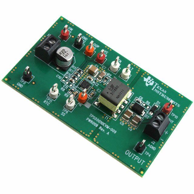
User's Guide SLVU459B–May2011–RevisedJuly2018 TPS55010EVM-009, Low-Power, Isolated Fly-Buck™ Converter This user's guide contains information for the TPS55010EVM-009 evaluation module (PWR009). Included aretheperformancespecifications,theschematic,andthebillofmaterialsfortheTPS55010EVM-009. Contents 1 Introduction................................................................................................................... 2 2 TestSetupandResults..................................................................................................... 3 3 BoardLayout................................................................................................................. 8 4 SchematicandBillofMaterials........................................................................................... 10 ListofFigures 1 TPS55010EVM-009Efficiency............................................................................................. 4 2 TPS55010EVM-009LoadRegulation..................................................................................... 4 3 TPS55010EVM-009LineRegulation,V =5V......................................................................... 5 IN 4 TPS55010EVM-009LoopResponse ..................................................................................... 5 5 TPS55010EVM-009OutputVoltageRipple ............................................................................. 6 6 TPS55010EVM-009InputVoltageRipple................................................................................ 6 7 TPS55010EVM-009Start-UpWithRisingV ........................................................................... 7 IN 8 TPS55010EVM-009TopAssembly....................................................................................... 8 9 TPS55010EVM-009TopCopper.......................................................................................... 9 10 TPS55010EVM-009BottomCopper...................................................................................... 9 11 TPS55010EVM-009Schematic.......................................................................................... 10 ListofTables 1 InputVoltageandOutputCurrentSummary............................................................................. 2 2 TPS55010EVM-009ElectricalandPerformanceSpecification........................................................ 2 3 EVMConnectorsandTestPoints......................................................................................... 3 4 BillofMaterials............................................................................................................. 11 Trademarks Fly-Buck,PowerPADaretrademarksofTexasInstruments. SLVU459B–May2011–RevisedJuly2018 TPS55010EVM-009,Low-Power,IsolatedFly-Buck™Converter 1 SubmitDocumentationFeedback Copyright©2011–2018,TexasInstrumentsIncorporated
Introduction www.ti.com 1 Introduction Thisuser'sguidecontainsbackgroundinformationfortheTPS55010aswellassupportdocumentationfor theTPS55010EVM-009evaluationmodule(PWR009).Includedaretheperformancespecifications,the schematic,andthebillofmaterialsfortheTPS55010EVM-009. 1.1 Background TheTPS55010dc/dcconverterisdesignedtoprovideuptoa200-mAoutputfromaninputvoltagesource of4.5Vto5.5V.Ratedinputvoltageandoutputcurrentrangefortheevaluationmodulearegivenin Table1.Thisevaluationmoduleisdesignedtodemonstratethesmall,printed-circuit-boardareasthatmay beachievedwhendesigningwiththeTPS55010regulator.Theswitchingfrequencyisexternallysetata nominal350kHz.Bothhigh-sideandlow-sideMOSFETsareincorporatedinsidetheTPS55010package alongwiththegatedrivecircuitry.Thelowdrain-to-sourceon-resistanceoftheMOSFETsallowsthe TPS55010toachievegoodefficiency.Thecompensationcomponentsareexternaltotheintegratedcircuit (IC),andanexternaldividerallowsforanadjustableoutputvoltage.Additionally,theTPS55010provides adjustableslow-startandundervoltagelockoutinputs.Theabsolutemaximuminputvoltageforthe TPS55010EVM-009is6V. Table1.InputVoltageandOutputCurrentSummary EVM InputVoltageRange OutputCurrentRange TPS55010EVM-009 V =4.5Vto6V 0Ato200mA IN 1.2 Performance Specification Summary AsummaryoftheTPS55010EVM-009performancespecificationsisprovidedinTable2.Specifications aregivenforaninputvoltageofV =5Vandanoutputvoltageof5V,unlessotherwisespecified.The IN TPS55010EVM-009isdesignedandtestedforV =4.5Vto6V.Theambienttemperatureis25°Cforall IN measurements,unlessotherwisenoted. Table2.TPS55010EVM-009ElectricalandPerformanceSpecification Parameter Condition MIN TYP MAX UNIT Outputvoltage 4.5V≤VIN≤5.5V,ILOAD≤200mA 5V 4.5 5 6 V Outputcurrent 4.5V≤VIN≤5.5V 0.2 A Outputripplevoltage,peak-to-peak ILOAD=200mA VIN=5V 20 mV Switchingfrequency ILOAD=200mA VIN=5V 350 kHz Efficiency,end-to-end ILOAD=200mA VIN=5V 85% Lineregulation ILOAD=200mA 4.5V≤VIN≤5.5V ±0.06 V Loadregulation ILOAD=10mAto200mA VIN=5V ±0.3 V Controlloopcrossoverfrequency ILOAD=200mA 25 kHz Slowstart 40 ms Operatingtemperature –25 85 °C 1.3 Modifications TheseevaluationmodulesaredesignedtoprovideaccesstothefeaturesoftheTPS55010.Some modificationscanbemadetothismodule. 1.3.1 InputVoltageRange TPS55010EVM-009canoperatefromaninputvoltageof5Vor3.3V,nominally.For3.3-Vnominalinput voltage,removeR3(allowstheEVMtostartupfromlowerinputvoltages),andchangeR9to511kΩ (changesswitchingfrequencyto200kHz). 2 TPS55010EVM-009,Low-Power,IsolatedFly-Buck™Converter SLVU459B–May2011–RevisedJuly2018 SubmitDocumentationFeedback Copyright©2011–2018,TexasInstrumentsIncorporated
www.ti.com TestSetupandResults 1.3.2 OperatingFrequency,Slow-Start,andUVLO Theoperatingfrequency,slow-starttime,andUVLOvoltagecanbeadjusted.R9setstheoperating frequency,C5setstheslow-starttime,andtheresistordividerofR2andR3setstheUVLOstartandstop voltages.SeetheTPS55010datasheet(SLVSAV0)fordetailsonadjustingtheseparameters. 1.3.3 ZenerDiodeandOutputSnubber Underno-loadconditions,VOUTcangetashighas15Vifoutputvoltagelimitingisnotprovided. TPS55010EVM-009providesaZenerdiode(5.6Vnominal)inserieswitharesistortolimittheoutput voltageatJ2to6V.TheZenerdiodepresentsanegligibleloadtothecircuitwithexternalloadsabove approximately3mAatJ2. PlaceholdersforanR-Csnubberareprovidedacrosstheoutputrectifier.Althoughthesnubberimpacts efficiency,itcanbeusedtodampentheringingacrosstherectifier. 2 Test Setup and Results Thissectiondescribeshowtoproperlyconnect,setup,andusetheTPS55010EVM-009evaluation module.Thesectionalsoincludestestresultstypicalfortheevaluationmoduleandcoversefficiency, outputvoltageregulation,loadtransients,loopresponse,outputripple,inputripple,andstart-up. 2.1 Input/Output Connections TheTPS55010EVM-009isprovidedwithinput/outputconnectorsandtestpointsasshowninTable3.A powersupplycapableofsupplying0.5AmustbeconnectedtoJ1throughapairof20AWGwires.The loadmustbeconnectedtoJ2throughapairof20AWGwires.Test-pointTP2providesaplacetomonitor theV inputvoltageswithTP5providingaconvenientgroundreference.TP10isusedtomonitorthe IN outputvoltagewithTP4asthegroundreference. Table3.EVMConnectorsandTestPoints Reference Label Description Designator J1 INPUT VINconnector J2 OUTPUT VOUTconnector TP2 VIN InputVINcircuitpoint TP5 GND InputGNDcircuitpoint TP10 VOUT OutputVOUTcircuitpoint TP4 AGND OutputAGNDcircuitpoint TP1 FAULT FAULTpin TP3 EN ENpin TP6 SS SLOWSTARTpin TP7 PH PHpin TP8 LOOP Injectionpointforloopmeasurements TP9 VC Regulatedvoltage TP12 GND InputGNDcircuitpoint SLVU459B–May2011–RevisedJuly2018 TPS55010EVM-009,Low-Power,IsolatedFly-Buck™Converter 3 SubmitDocumentationFeedback Copyright©2011–2018,TexasInstrumentsIncorporated
TestSetupandResults www.ti.com 2.2 Efficiency Figure1 showstheefficiencyfortheTPS55010EVM-009atanambienttemperatureof25°C. 100 90 80 70 %) 60 y ( nc 50 e ci Effi 40 30 20 10 Vin = 5 V 0 0 0.05 0.1 0.15 0.2 0.25 0.3 Load Current (A) C001 Figure1.TPS55010EVM-009Efficiency Theefficiencymaybelowerathigherambienttemperatures,duetotemperaturevariationinthedrain-to- sourceresistanceoftheinternalMOSFET. 2.3 Load Regulation Figure2 showstheloadregulationfortheTPS55010EVM-009atanambienttemperatureof25°C. 6.5 Vin = 5 V 6 V) e ( 5.5 g a olt V ut utp 5 O 4.5 4 0 0.05 0.1 0.15 0.2 0.25 0.3 Load Current (A) C002 Figure2.TPS55010EVM-009LoadRegulation 4 TPS55010EVM-009,Low-Power,IsolatedFly-Buck™Converter SLVU459B–May2011–RevisedJuly2018 SubmitDocumentationFeedback Copyright©2011–2018,TexasInstrumentsIncorporated
www.ti.com TestSetupandResults 2.4 Line Regulation Figure3 showsthelineregulationfortheTPS55010EVM-009atanambienttemperatureof25°C. 6 5.5 V) e ( g a olt 5 V ut p ut O 4.5 Iout = 10 mA Iout = 50 mA Iout = 200 mA 4 4 4.5 5 5.5 6 Input Voltage (V) C003 Figure3.TPS55010EVM-009LineRegulation,V =5V IN 2.5 Loop Characteristics TheTPS55010EVM-009loop-responsecharacteristicsareshowninFigure4.Gainandphaseplotsare shownforV =5Vandaloadcurrentofboth0mAand200mA.Ata0-mAload,theunitygain IN bandwidthis32.5kHzandphasemarginis53degrees.Ata200-mAload,theunitygainbandwidthis 25.2kHzandthephasemarginis82degrees. 60 180 40 120 20 60 Gain (dB) 0 0-mA Load Gain 0 (cid:131)Phase () –20 –60 200-mA Load Gain –40 0-mA Load Phase –120 200-mA Load Phase –60 –180 1 0 1 0 0 1 k 1 0 k 1 0 0 k 1 M Frequency (Hz) C004 Figure4.TPS55010EVM-009LoopResponse SLVU459B–May2011–RevisedJuly2018 TPS55010EVM-009,Low-Power,IsolatedFly-Buck™Converter 5 SubmitDocumentationFeedback Copyright©2011–2018,TexasInstrumentsIncorporated
TestSetupandResults www.ti.com 2.6 Output Voltage Ripple TheTPS55010EVM-009outputvoltagerippleisshowninFigure5 .Theoutputcurrentistheratedfull loadof200mAandV =5V.Theripplevoltageismeasureddirectlyacrosstheoutputcapacitors. IN Figure5.TPS55010EVM-009OutputVoltageRipple 2.7 Input Voltage Ripple TheTPS55010EVM-009inputvoltagerippleisshowninFigure6 .Theoutputcurrentistheratedfullload of200mAandV =5V.Theripplevoltageismeasureddirectlyacrosstheinputcapacitors. IN Figure6.TPS55010EVM-009InputVoltageRipple 2.8 Powering Up Figure7 showsthestart-upwaveformswithrisingV andtheoutputloadedwith22 Ω.InFigure7,the IN outputstartstorisewhenV reachestherisingUVLOof4.5V. IN 6 TPS55010EVM-009,Low-Power,IsolatedFly-Buck™Converter SLVU459B–May2011–RevisedJuly2018 SubmitDocumentationFeedback Copyright©2011–2018,TexasInstrumentsIncorporated
www.ti.com TestSetupandResults VIN V = 2 V/div IN EN V = 500 mV/div EN V = 2 V/div O VOUT t - Time = 5 ms/div Figure7.TPS55010EVM-009Start-UpWithRisingV IN SLVU459B–May2011–RevisedJuly2018 TPS55010EVM-009,Low-Power,IsolatedFly-Buck™Converter 7 SubmitDocumentationFeedback Copyright©2011–2018,TexasInstrumentsIncorporated
BoardLayout www.ti.com 3 Board Layout ThissectionprovidesadescriptionoftheTPS55010EVM-009,boardlayout,andlayerillustrations. 3.1 Layout TheboardlayoutfortheTPS55010EVM-009isshowninFigure8 throughFigure10.Thetop-sidelayerof theEVMislaidoutinamannertypicalofauserapplication.Thetopandbottomlayersare2-ozcopper.A basicsetoflayoutguidelinesinclude: • PlacetheinputcapacitorsclosetotheTPS55010VINandGNDterminals. • Arrangethetransformer,inputcapacitors,andtheregulatedvoltagecapacitorinamannertominimize looparea. • ConnecttheGNDendoftheanalogcontrolcircuitry(COMP,VSENSE,RT/CLK,andSSpins)together apartfromthemainpowerGND.ReferencethisanalogGNDtrace/shapetothepowerGND (PowerPAD™ICpackageofTPS55010)atasinglepoint. • ThePowerPAD™packageoftheTPS55010providesameanstoremoveheatfromthedeviceand mustbeconnectedtotheGNDplanewithmultipleviasasshownintheTPS55010datasheet, SLVSAV0. Figure8.TPS55010EVM-009TopAssembly 8 TPS55010EVM-009,Low-Power,IsolatedFly-Buck™Converter SLVU459B–May2011–RevisedJuly2018 SubmitDocumentationFeedback Copyright©2011–2018,TexasInstrumentsIncorporated
www.ti.com BoardLayout Figure9.TPS55010EVM-009TopCopper Figure10.TPS55010EVM-009BottomCopper 3.2 Estimated Circuit Area Theestimatedprinted-circuitboardareaforthecomponentsusedinthisdesignis0.70in2.Thisareadoes notincludetestpointsorconnectors. SLVU459B–May2011–RevisedJuly2018 TPS55010EVM-009,Low-Power,IsolatedFly-Buck™Converter 9 SubmitDocumentationFeedback Copyright©2011–2018,TexasInstrumentsIncorporated
SchematicandBillofMaterials www.ti.com 4 Schematic and Bill of Materials ThissectionpresentstheTPS55010EVM-009schematicandbillofmaterials. 4.1 Schematic Figure11istheschematicfortheTPS55010EVM-009. EN FAULT TP3 TP1 VIN TP2 R1 VIN 100k 5 +/- 0.5V J1 AGND VIN 1 TP4 GND 2 R2 C4 71.5k + C22102µGFND C471µF C0.21µF R3 17PWRPD16VIN15EN14FAULT13BOOT C0.31µFSS PH 1000pF 2kV D1 TP5 26.7k 1 VIN1 PH 12 TP6 TP7 T1 BZT52C5V6 2 VIN2 U1 PH 11 750311880 3 GND TPS55010RTE PH 10 2 8 VOUT 4 GND SS 9 R5 4 7 C6 R6 2R004 52 0+0/m- 0A.5V GND VSENSE COMP RT/CLK C0.51uF TP8 R749.9 TP9 6 D12000pF 2100 12 J2 AGND 5 6 7 8 LOOP 100k VC 5 +VOUT B120-13-F C7 TP10 47µF VOUT C8 C9 GND 10µF 10µF R8 TP12 10.5k NOTES R10 1 Not Installed C10 C11 R9 61.9k 3900pF 100pF 280k Figure11.TPS55010EVM-009Schematic 10 TPS55010EVM-009,Low-Power,IsolatedFly-Buck™Converter SLVU459B–May2011–RevisedJuly2018 SubmitDocumentationFeedback Copyright©2011–2018,TexasInstrumentsIncorporated
www.ti.com SchematicandBillofMaterials 4.2 Bill of Materials Table4presentsthebillofmaterialsfortheTPS55010EVM-009. Table4.BillofMaterials Count RefDes Value Description Size PartNumber MFR 2 C1,C7 47µF Capacitor,Ceramic,10V,X5R,10% 1210 Std Std 3 C2,C3,C5 0.1µF Capacitor,Ceramic,LowInductance,16V, 0603 Std Std X7R,10% 1 C4 1000pF Capacitor,Ceramic,2kV,X7R,10% 1210 Std Std 1 C6 1000pF Capacitor,Ceramic,LowInductance,16V, 0603 Std Std X7R,10% 2 C8,C9 10µF Capacitor,Ceramic,10V,X5R,10% 1210 Std Std 1 C10 3900pF Capacitor,Ceramic,50V,X7R,10% 0603 Std Std 1 C11 100pF Capacitor,Ceramic,50V,NP0,5% 0603 Std Std 1 C12 220µF Capacitor,Aluminum,6.3V,±20% 0.260x0.276inch EEE-FK0J221P Panasonic 1 D1 BZT52C5V6 Diode,Zener,PlanarPower,500mW,5.6V SOD-123 BZT52C5V6-7-F Diodes,Inc 1 D2 B120-13-F Diode,Schottky,1000-mA,20-V SMA B120-13-F Diodes,Inc 2 J1,J2 ED555/2DS TerminalBlock,2-pin,6-A,3.5mm 0.27x0.25inch ED555/2DS OST 2 R1,R7 100k Resistor,Chip,1/16W,1% 0603 Std Std 1 R2 71.5k Resistor,Chip,1/16W,1% 0603 Std Std 1 R3 26.7k Resistor,Chip,1/16W,1% 0603 Std Std 1 R4 200 Resistor,Chip,1/16W,1% 0603 Std Std 1 R5 49.9 Resistor,Chip,1/16W,1% 0603 Std Std 1 R6 200 Resistor,Chip,1/16W,1% 0603 Std Std 0 R8 DNP Resistor,Chip,1/16W,1% 0603 Std Std 1 R9 280k Resistor,Chip,1/16W,1 0603 Std Std 1 R10 61.9k Resistor,Chip,1/16W,1 0603 Std Std 4 TP1,TP3, 5012 TestPoint,White,ThruHole 0.125x0.125inch 5010 Keystone TP6 3 TP2,TP9, 5010 TestPoint,Black,ThruHole 0.125x0.125inch 5010 Keystone TP10 3 TP4,TP5, 5011 TestPoint,Black,ThruHole 0.125x0.125inch 5011 Keystone TP12 2 TP7,TP8 5013 TestPoint,Orange,ThruHole 0.125x0.125inch 5013 Keystone 1 T1 2.5µH Transformer,±10% 0.410x0.510inch 750311880 Wurth 1 U1 TPS55010RTE IC,DC-DCConverter QFN-16 TPS55010RTE TI 1 -- PCB,2.5Inx1.5Inx0.062In 2.5"x2.5"x0.062" PWR009 Any SLVU459B–May2011–RevisedJuly2018 TPS55010EVM-009,Low-Power,IsolatedFly-Buck™Converter 11 SubmitDocumentationFeedback Copyright©2011–2018,TexasInstrumentsIncorporated
RevisionHistory www.ti.com Revision History NOTE:Pagenumbersforpreviousrevisionsmaydifferfrompagenumbersinthecurrentversion. ChangesfromARevision(June2014)toBRevision .................................................................................................... Page • ChangedschematicvaluesofR7from16.5kto100kandR10from10.0kto61.9k.......................................... 10 12 RevisionHistory SLVU459B–May2011–RevisedJuly2018 SubmitDocumentationFeedback Copyright©2011–2018,TexasInstrumentsIncorporated
www.ti.com RevisionHistory ChangesfromOriginal(May2011)toARevision................................................................................................................ Page • Changed7Vto6Vinbackgroundsection............................................................................................ 2 • Changed3Vto4.5Vintheinputvoltageandoutputcurrentsummarytableandinthefirstparagraphoftheperformance specificationsummarysection........................................................................................................... 2 • Changedcontentoftheelectricalandperformancespecificationtable............................................................ 2 • Changedefficiencygraph................................................................................................................ 4 • Changedloadregulationgraph.......................................................................................................... 4 • Deletedlineregulation,VIN=3.3Vgraph............................................................................................. 5 • Changedlineregulationgraph........................................................................................................... 5 • ChangedPCBlayoutimages............................................................................................................ 8 • Changedschematicdiagram........................................................................................................... 10 • ChangedBOM:movedC7,changedcontentofC10andC11rows. ............................................................ 11 SLVU459B–May2011–RevisedJuly2018 RevisionHistory 13 SubmitDocumentationFeedback Copyright©2011–2018,TexasInstrumentsIncorporated
IMPORTANTNOTICEFORTIDESIGNINFORMATIONANDRESOURCES TexasInstrumentsIncorporated(‘TI”)technical,applicationorotherdesignadvice,servicesorinformation,including,butnotlimitedto, referencedesignsandmaterialsrelatingtoevaluationmodules,(collectively,“TIResources”)areintendedtoassistdesignerswhoare developingapplicationsthatincorporateTIproducts;bydownloading,accessingorusinganyparticularTIResourceinanyway,you (individuallyor,ifyouareactingonbehalfofacompany,yourcompany)agreetouseitsolelyforthispurposeandsubjecttothetermsof thisNotice. TI’sprovisionofTIResourcesdoesnotexpandorotherwisealterTI’sapplicablepublishedwarrantiesorwarrantydisclaimersforTI products,andnoadditionalobligationsorliabilitiesarisefromTIprovidingsuchTIResources.TIreservestherighttomakecorrections, enhancements,improvementsandotherchangestoitsTIResources. Youunderstandandagreethatyouremainresponsibleforusingyourindependentanalysis,evaluationandjudgmentindesigningyour applicationsandthatyouhavefullandexclusiveresponsibilitytoassurethesafetyofyourapplicationsandcomplianceofyourapplications (andofallTIproductsusedinorforyourapplications)withallapplicableregulations,lawsandotherapplicablerequirements.You representthat,withrespecttoyourapplications,youhaveallthenecessaryexpertisetocreateandimplementsafeguardsthat(1) anticipatedangerousconsequencesoffailures,(2)monitorfailuresandtheirconsequences,and(3)lessenthelikelihoodoffailuresthat mightcauseharmandtakeappropriateactions.YouagreethatpriortousingordistributinganyapplicationsthatincludeTIproducts,you willthoroughlytestsuchapplicationsandthefunctionalityofsuchTIproductsasusedinsuchapplications.TIhasnotconductedany testingotherthanthatspecificallydescribedinthepublisheddocumentationforaparticularTIResource. Youareauthorizedtouse,copyandmodifyanyindividualTIResourceonlyinconnectionwiththedevelopmentofapplicationsthatinclude theTIproduct(s)identifiedinsuchTIResource.NOOTHERLICENSE,EXPRESSORIMPLIED,BYESTOPPELOROTHERWISETO ANYOTHERTIINTELLECTUALPROPERTYRIGHT,ANDNOLICENSETOANYTECHNOLOGYORINTELLECTUALPROPERTY RIGHTOFTIORANYTHIRDPARTYISGRANTEDHEREIN,includingbutnotlimitedtoanypatentright,copyright,maskworkright,or otherintellectualpropertyrightrelatingtoanycombination,machine,orprocessinwhichTIproductsorservicesareused.Information regardingorreferencingthird-partyproductsorservicesdoesnotconstitutealicensetousesuchproductsorservices,orawarrantyor endorsementthereof.UseofTIResourcesmayrequirealicensefromathirdpartyunderthepatentsorotherintellectualpropertyofthe thirdparty,oralicensefromTIunderthepatentsorotherintellectualpropertyofTI. TIRESOURCESAREPROVIDED“ASIS”ANDWITHALLFAULTS.TIDISCLAIMSALLOTHERWARRANTIESOR REPRESENTATIONS,EXPRESSORIMPLIED,REGARDINGTIRESOURCESORUSETHEREOF,INCLUDINGBUTNOTLIMITEDTO ACCURACYORCOMPLETENESS,TITLE,ANYEPIDEMICFAILUREWARRANTYANDANYIMPLIEDWARRANTIESOF MERCHANTABILITY,FITNESSFORAPARTICULARPURPOSE,ANDNON-INFRINGEMENTOFANYTHIRDPARTYINTELLECTUAL PROPERTYRIGHTS. TISHALLNOTBELIABLEFORANDSHALLNOTDEFENDORINDEMNIFYYOUAGAINSTANYCLAIM,INCLUDINGBUTNOT LIMITEDTOANYINFRINGEMENTCLAIMTHATRELATESTOORISBASEDONANYCOMBINATIONOFPRODUCTSEVENIF DESCRIBEDINTIRESOURCESOROTHERWISE.INNOEVENTSHALLTIBELIABLEFORANYACTUAL,DIRECT,SPECIAL, COLLATERAL,INDIRECT,PUNITIVE,INCIDENTAL,CONSEQUENTIALOREXEMPLARYDAMAGESINCONNECTIONWITHOR ARISINGOUTOFTIRESOURCESORUSETHEREOF,ANDREGARDLESSOFWHETHERTIHASBEENADVISEDOFTHE POSSIBILITYOFSUCHDAMAGES. YouagreetofullyindemnifyTIanditsrepresentativesagainstanydamages,costs,losses,and/orliabilitiesarisingoutofyournon- compliancewiththetermsandprovisionsofthisNotice. ThisNoticeappliestoTIResources.Additionaltermsapplytotheuseandpurchaseofcertaintypesofmaterials,TIproductsandservices. Theseinclude;withoutlimitation,TI’sstandardtermsforsemiconductorproductshttp://www.ti.com/sc/docs/stdterms.htm),evaluation modules,andsamples(http://www.ti.com/sc/docs/sampterms.htm). MailingAddress:TexasInstruments,PostOfficeBox655303,Dallas,Texas75265 Copyright©2018,TexasInstrumentsIncorporated