ICGOO在线商城 > 集成电路(IC) > PMIC - 监控器 > MAX6767TALD2+T

 Datasheet下载
- 型号: MAX6767TALD2+T
- 制造商: Maxim
- 库位|库存: xxxx|xxxx
- 要求:
| 数量阶梯 | 香港交货 | 国内含税 |
| +xxxx | $xxxx | ¥xxxx |
查看当月历史价格
查看今年历史价格
MAX6767TALD2+T产品简介:
ICGOO电子元器件商城为您提供MAX6767TALD2+T由Maxim设计生产,在icgoo商城现货销售,并且可以通过原厂、代理商等渠道进行代购。 MAX6767TALD2+T价格参考。MaximMAX6767TALD2+T封装/规格:PMIC - 监控器, 开路漏极或开路集电极 监控器 1 通道 8-TDFN-EP(3x3)。您可以下载MAX6767TALD2+T参考资料、Datasheet数据手册功能说明书,资料中有MAX6767TALD2+T 详细功能的应用电路图电压和使用方法及教程。
MAX6767TALD2+T 是由 Maxim Integrated(现已被 Analog Devices 收购)生产的一款 PMIC(电源管理集成电路)监控器。该器件主要用于监控和保护系统中的电压、电流和其他关键参数,确保电子设备在正常工作范围内运行,并在出现异常时采取适当的保护措施。

 应用场景:

1. 工业控制系统:
   MAX6767TALD2+T 可用于工业自动化设备中,如PLC(可编程逻辑控制器)、传感器接口模块等。它能够实时监控电源电压,防止因电压波动导致的系统故障或数据丢失。此外,它还可以检测过流、短路等异常情况,及时触发保护机制,延长设备寿命。

2. 通信设备:
   在通信基站、路由器、交换机等网络设备中,MAX6767TALD2+T 可以确保电源系统的稳定性和可靠性。它能够监控多个电源轨的状态,提供精确的电压监测和快速响应的保护功能,保障通信链路的连续性。

3. 消费电子产品:
   该器件适用于智能手机、平板电脑、笔记本电脑等便携式设备。它可以监控电池电压和充电状态,防止过度充电或放电,从而保护电池并提高设备的安全性。同时,它还能在电源异常时自动关闭设备,避免硬件损坏。

4. 汽车电子:
   在汽车电子系统中,MAX6767TALD2+T 可用于车载信息娱乐系统、ADAS(高级驾驶辅助系统)等模块。它能够监控车辆电源的稳定性,确保各个子系统的正常工作。特别是在电动汽车中,它可以帮助监控高压电池组的状态,确保安全驾驶。

5. 医疗设备:
   对于医疗仪器如监护仪、呼吸机等,MAX6767TALD2+T 可以确保电源的可靠性和安全性。它能够实时监控电源电压,防止因电源问题导致的设备故障,确保患者的安全。

 总结:
MAX6767TALD2+T 具有高精度的电压监控和快速响应的保护功能,适用于多种应用场景,尤其是在对电源稳定性和安全性要求较高的领域。其广泛的应用范围和可靠的性能使其成为许多电子系统中不可或缺的一部分。
| 参数 | 数值 |
| 产品目录 | 集成电路 (IC) |
| 描述 | IC REG LINEAR 5V/ADJ 8TDFN |
| 产品分类 | |
| 品牌 | Maxim Integrated |
| 数据手册 | |
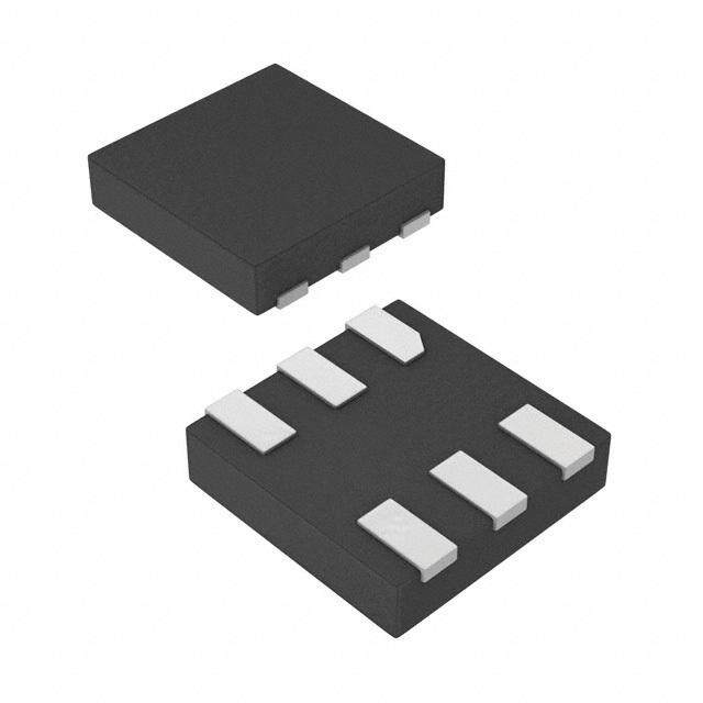
| 产品图片 |
|
| 产品型号 | MAX6767TALD2+T |
| rohs | 无铅 / 符合限制有害物质指令(RoHS)规范要求 |
| 产品系列 | - |
| 产品培训模块 | http://www.digikey.cn/PTM/IndividualPTM.page?site=cn&lang=zhs&ptm=25703http://www.digikey.cn/PTM/IndividualPTM.page?site=cn&lang=zhs&ptm=25705 |
| 供应商器件封装 | 8-TDFN-EP(3x3) |
| 其它名称 | MAX6767TALD2+TCT |
| 其它有关文件 | |
| 包装 | 剪切带 (CT) |
| 受监控电压数 | 1 |
| 复位 | 低有效 |
| 复位超时 | 最小为 8.75 ms |
| 安装类型 | 表面贴装 |
| 封装/外壳 | 8-WDFN 裸露焊盘 |
| 工作温度 | -40°C ~ 125°C |
| 应用说明 | |
| 标准包装 | 1 |
| 电压-阈值 | 4.625V,可调 |
| 类型 | 稳压器/监控器 |
| 输出 | 开路漏极或开路集电极 |


PDF Datasheet 数据手册内容提取
EVALUATION KIT AVAILABLE MAX6765–MAX6774 Automotive Micropower Linear Regulators with Supervisor General Description Features The MAX6765–MAX6774B are low-quiescent-current, ● Low 31μA Quiescent Current high-voltage linear regulators that operate from 4V to 72V ● 4V to 72V Wide Input Voltage Range and deliver up to 100mA of load current. These low-power ● 100mA Output Current Capability devices consume only 31µA of quiescent current, mak- ● Dropout Voltage of 620mV with 5V Output at 100mA ing them ideal for always-on automotive modules. These ● Fixed Output-Voltage Options: 5V, 3.3V, 2.5V, and devices are offered with fixed standard output options of 1.8V 5.0V, 3.3V, 2.5V, and 1.8V, or can be adjusted from 1.8V ● Watchdog Timer Option (1.6s (MAX6773/MAX6774) to 11V with two external resistors. and 50ms (MAX6773B/MAX6774B)) The MAX6765–MAX6774B feature a push-pull or open- ● Adjustable Output Voltages from 1.8V to 11V drain, active-low RESET output with either fixed or adjustable ● Open-Drain or Push-Pull RESET Output thresholds. Whenever the regulator’s output falls below ● Fixed or Capacitor-Adjustable Reset Timeouts the reset threshold, the RESET output asserts and remains asserted for at least the minimum reset timeout ● Small, Thermally Enhanced 1.9W, 3mm x 3mm period after the output voltage exceeds its threshold. The TDFN Package minimum reset timeout period is offered with fixed values ● Overtemperature and Short-Circuit Protection from 75µs to 200ms or can be adjusted externally with a ● Fully Specified from -40°C to +125°C small capacitor. ● AEC-Q100 qualified (MAX6765TT_D_/V+, These devices provide three regulator enable modes MAX6767TA_D_/V+, MAX6769TA_D_/V+, to accommodate several power-on schemes. The MAX6773TA_D_/V+ , MAX6773BTA_D_/V+ only) MAX6765/MAX6766/MAX6769/MAX6770/MAX6773/ Ordering Information MAX6773B/MAX6774/MAX6774B feature a single tradi- tional enable input (ENABLE) to turn on and off the regu- TEMP PIN- PART lator. The MAX6771/MAX6772 provide dual enable inputs RANGE PACKAGE (ENABLE1 and ENABLE2) to turn on and off the regulator MAX6765TT_D_+ -40°C to +125°C 6 TDFN-EP* either through an ignition switch or a bus transceiver. The MAX6765TT_D_/V+ -40°C to +125°C 6 TDFN-EP* MAX6767/MAX6768 provide a hold input (HOLD) in addi- tion to the enable input to allow for the implementation of a Ordering Information continued at end of data sheet. self-holding circuit without requiring external components. The first “_” is a placeholder for the voltage output and reset Setting HOLD low after enabling the regulator forces the threshold. The 2nd “_” designates the fixed reset-timeout option. regulator to remain on even if ENABLE is subsequently See Tables 1 and 2 for details. For example, the MAX6765TTLD4 set low. Releasing HOLD shuts down the regulator. has a 5V output, a reset threshold of 4.65V, and a 200ms typical reset timeout. The MAX6773/MAX6773B/MAX6774/MAX6774B also +Denotes a lead(Pb)-free/RoHS-compliant package. include a watchdog input that monitors a pulse train from /V denotes an automotive qualified part. the microprocessor (µP) and generates a reset pulse if *EP = Exposed pad. the watchdog input remains high or low for a duration For tape-and-reel orders add a “T” after the “+” symbol to com- longer than the 1.6s (typ) (MAX6773/MAX6774) or 50ms plete the part number. Tape-and-reel orders are available in 2.5k increments. Nonstandard versions require a 10k minimum (typ) (MAX6773B/MAX6774B) watchdog timeout period. order quantity. The MAX6765–MAX6774B are available in a small, ther- Pin Configurations mally enhanced 3mm x 3mm TDFN package that can dreisgsuiplaatoter uopp etroa ti1o.n9 5d1uWri,n gth ehriegbhy asmupbpieonrtt integm cpoenrtaintuuroeuss, TOP VIEW OUT TIMEOUT RESET high battery voltage, and high load-current conditions. 6 5 4 The MAX6765–MAX6774B are fully specified for a -40°C to +125°C operating temperature range. MAX6765 MAX6766 Applications EP + ● Automotive 1 2 3 ●● ITnedleucsotrmial IN TDGNDFN ENABLE Pin Configurations continued at end of data sheet. Typical Application Circuit and Selector Guide appear at end of data sheet. 19-0657; Rev 9; 8/17
MAX6765–MAX6774 Automotive Micropower Linear Regulators with Supervisor Absolute Maximum Ratings (All pins referenced to GND, unless otherwise noted.) 8-Pin TDFN 3mm x 3mm VIN .........................................................................-0.3V to +80V (derate 24.4mW/°C above +70°C) .........................1951.2mW OUT ..............................................-0.3V to min (12V, IN + 0.3V) Operating Temperature Range .........................-40°C to +125°C ENABLE, ENABLE1, ENABLE2 ...................-0.3V to (IN + 0.3V) Junction Temperature ......................................................+150°C RESET (open-drain output), TIMEOUT, WDI, Storage Temperature Range ............................-65°C to +150°C RESETIN, SET ....................................................-0.3V to 12V Lead Temperature (soldering, 10s) .................................+300°C RESET (push-pull output), HOLD ............-0.3V to (OUT + 0.3V) Soldering Temperature (reflow) .......................................+260°C Maximum Current (all pins except IN and OUT) ................50mA Continuous Power Dissipation (TA = +70°C) 6-Pin TDFN 3mm x 3mm (derate 23.8mW/°C above +70°C) .........................1904.8mW Stresses beyond those listed under “Absolute Maximum Ratings” may cause permanent damage to the device. These are stress ratings only, and functional operation of the device at these or any other conditions beyond those indicated in the operational sections of the specifications is not implied. Exposure to absolute maximum rating conditions for extended periods may affect device reliability. Electrical Characteristics (VIN = 14V, CIN = 0.1μF, COUT = 10μF, TA = TJ = -40°C to +125°C, unless otherwise noted. Typical values are at TA = TJ = +25°C.) (Note 1) PARAMETER SYMBOL CONDITIONS MIN TYP MAX UNITS Supply Voltage Range VIN 4 72 V ILOAD = 0A 31 45 ILOAD = 50mA 35 50 Supply Current (MAX6765–MAX6772) (Note 2) ILOAD = 100mA, VIN = 14V 37 55 µA ILOAD = 0A, VIN = 42V 35 50 ILOAD = 10mA, VIN = 42V 37 55 ILOAD = 0A 38 50 Supply Current ILOAD = 50mA 42 55 (MAX6773/MAX6773B/ MAX6774/MAX6774B) ILOAD = 100mA 44 60 µA (Note 2) ILOAD = 0A, VIN = 42V 42 55 ILOAD = 10mA, VIN = 42V 44 60 Shutdown Supply Current ISHDN ENABLE , ENABLE1, ENABLE2 = GND 3.3 7 µA L/M, ILOAD = 1mA 4.925 5 5.075 L/M, 1mA ≤ ILOAD ≤ 100mA, VIN = 11V 4.850 5 5.150 T/S, ILOAD = 1mA 3.251 3.3 3.350 T/S, 1mA ≤ ILOAD ≤ 100mA, VIN = 9.3V 3.201 3.3 3.399 Output Voltage VOUT V Z/Y, ILOAD = 1mA 2.463 2.5 2.538 Z/Y, 1mA ≤ ILOAD ≤ 100mA, VIN = 8.5V 2.425 2.5 2.575 W/V, ILOAD = 1mA 1.773 1.8 1.827 W/V, 1mA ≤ ILOAD ≤ 100mA, VIN = 7.8V 1.746 1.8 1.854 Adjustable Output Voltage Range VOUT 1.8 11.0 V SET Threshold Voltage (MAX6767–MAX6774) VSET ILOAD = 1mA 1.20 1.233 1.26 V SET rising 116 Dual Mode™ SET Threshold mV SET falling 58 Dual Mode is a trademark of Maxim Integrated Products, Inc. www.maximintegrated.com Maxim Integrated │ 2
MAX6765–MAX6774 Automotive Micropower Linear Regulators with Supervisor Electrical Characteristics (continued) (VIN = 14V, CIN = 0.1μF, COUT = 10μF, TA = TJ = -40°C to +125°C, unless otherwise noted. Typical values are at TA = TJ = +25°C.) (Note 1) PARAMETER SYMBOL CONDITIONS MIN TYP MAX UNITS SET Input Current (MAX6767–MAX6774) ISET VSET = 1.5V, VIN = 11V -100 +100 nA L/M, 5V output option, ILOAD = 10mA 60 130 L/M, 5V output option, ILOAD = 50mA 300 630 Dropout Voltage (Note 3) ΔVDO mV L/M, 5V output option, ILOAD = 100mA 620 1200 T/S, 3.3V output option, ILOAD = 100mA 866 1600 Guaranteed Output Current 100 mA (Note 4) Output Current Limit Output shorted to GND, VIN = 14V 150 250 mA Thermal-Shutdown Temperature 160 °C Thermal-Shutdown Hysteresis 20 °C Line Regulation 6.5V ≤ VIN ≤ 72V, ILOAD = 1mA 1 % Load Regulation IOUT = 1mA to 100mA, 1.5 % (MAX6767–MAX6774) VIN = VOUT(NOM) + 6V Power-Supply Rejection Ratio PSRR ILOAD = 10mA, fIN = 100Hz, 500mVP-P 70 dB From ENABLE high to OUT, Startup Response Time tSTART ILOAD = 100mA 180 µs Output Overvoltage Protection 1.07 x 1.1 x 1.13 x Threshold OVTH ISINK = 1mA (from OUT) VOUT VOUT VOUT V Output Overvoltage Protection Maximum Sink Current OUT = OUT(NOM) x 1.15 5 10 mA LOGIC INPUT (ENABLE, ENABLE1, ENABLE2, HOLD) Input Low Voltage VIL ENABLE, ENABLE1, ENABLE2 0.4 V Input High Voltage VIH ENABLE, ENABLE1, ENABLE2 1.4 V ENABLE, ENABLE1, ENABLE2 ENABLE, ENABLE1, ENABLE2 are 0.6 µA Input Pulldown Current internally pulled down to GND VIL 1.8V ≤ VOUT ≤ 11V 0.4 HOLD Input Threshold Voltage OUT - V VIH 1.8V ≤ VOUT ≤ 11V 0.4 HOLD Input Pullup Current HOLD is internally pulled up to OUT 1.8 µA RESET OUTPUT L 4.500 4.625 4.750 M 4.250 4.375 4.500 T 2.970 3.053 3.135 SET = GND, S 2.805 2.888 2.970 RESET Threshold V RESET falling Z 2.250 2.313 2.375 Y 2.125 2.188 2.250 W 1.620 1.665 1.710 V 1.530 1.575 1.620 www.maximintegrated.com Maxim Integrated │ 3
MAX6765–MAX6774 Automotive Micropower Linear Regulators with Supervisor Electrical Characteristics (continued) (VIN = 14V, CIN = 0.1μF, COUT = 10μF, TA = TJ = -40°C to +125°C, unless otherwise noted. Typical values are at TA = TJ = +25°C.) (Note 1) PARAMETER SYMBOL CONDITIONS MIN TYP MAX UNITS L/T/Z/W, SET = resistive divider, RESET VOUT x VOUT VOUT RESET Threshold (Adjustable falling 0.9 x 0.925 x 0.950 V Output Voltage) M/S/Y/V, SET = resistive divider, RESET VOUT VOUT VOUT falling x 0.85 x 0.875 x 0.900 RESETIN Input Current VRESETIN = VGND or 12V -100 +100 nA VTH = 87.5% of VSET (M/S/Y/V), 1.057 1.085 1.112 RESET falling RESETIN Threshold V VTH = 92.5% of VSET (L/T/Z/W), 1.118 1.147 1.176 RESET falling OUT to RESET Delay VOUT falling 0.3 µs RESETIN To RESET Delay RESETIN falling 35 µs D0 75 µs D1 2.187 3.125 4.063 RESET Timeout Period VOUT rising D2 8.75 12.5 16.25 (TIMEOUT Connected to OUT) ms D3 35 50 65 D4 140 200 260 TIMEOUT Ramp Current 800 1000 1200 nA L/M/T/S options 1.160 1.220 1.259 TIMEOUT Ramp Threshold V V/W/Y/Z options 1.060 1.170 1.242 VOUT ≥ 1.8V, ISINK = 50µA, 0.3 RESET Output-Voltage Low RESET asserted VOL V (Open Drain or Push-Pull) VOUT ≥ 1.8V, ISINK = 3.2mA, 0.4 RESET asserted R(PEuSsEh-TP Oulul)tput-Voltage High VOH VROEUSTE T≥ n1o.8t Va,s IsSeOrUteRdCE = 250µA, V0O.8U xT V RESET Open-Drain Leakage RESET not asserted, RESET = 12V 100 nA Current Watchdog Minimum Input Pulse tWDI 1.8V ≤ VOUT ≤ 11V 1 µs Watchdog Input Low Voltage VIL 1.8V ≤ VOUT ≤ 11V 0.4 V Watchdog Input High Voltage VIH 1.8V ≤ VOUT ≤ 11V VOUT - 0.4V V Watchdog Input Low Voltage VIL 1.8V ≤ VOUT ≤ 11V 0.4 V Watchdog Input Current IWDI VWDI = 0V or VWDI = 12V -1 +1 µA MAX6773/MAX6774 1.12 1.6 2.08 s Watchdog Timeout Period tWD MAX6773B/MAX6774B 40 50 60 ms Note 1: Production tested at TA = +25°C. Overtemperature limits are guaranteed by design. Note 2: Device tested at internally set voltage. Note 3: Dropout voltage for L/M versions is defined as (VIN - VOUT) when VOUT equals 98% of the nominal value of VOUT when VIN = 11V. For T/S versions, dropout voltage is defined as (VIN - VOUT) when VOUT equals 98% of the nominal value of VOUT when VIN = 9.3V. Note 4: Observe the absolute maximum power dissipation limits. www.maximintegrated.com Maxim Integrated │ 4
MAX6765–MAX6774 Automotive Micropower Linear Regulators with Supervisor Typical Operating Characteristics (VIN = 14V, COUT = 10μF, CIN = 0.1μF, TA = +25°C, unless otherwise noted.) SHUTDOWN SUPPLY CURRENT SUPPLY CURRENT vs. INPUT VOLTAGE SUPPLY CURRENT vs. TEMPERATURE vs. TEMPERATURE 444204 LDIIMSISTIEPDA TBIOY NPVOOWUTE =R 3.3V MAX6765 toc01 444537 VOUT = 5V MAX6765 toc02 T (µA) 45..50 MAX6765 toc03 RENT (µA) 3368 ILOAD = 100mA RENT (µA) 3491 ILOAD = 100mA ILOAD = 50mA Y CURREN 34..50 UR 34 UR 37 PL 3.0 PPLY C 32 ILOAD = 0 PPLY C 35 ILOAD = 1mA WN SUP 2.5 SU 30 SU 33 DO 2.0 28 31 UT H S 1.5 26 29 ILOAD = 0 24 27 1.0 4 12 20 28 36 44 52 60 68 -40 -25 -10 5 20 35 50 65 80 95 110125 -40 -25 -10 5 20 35 50 65 80 95 110125 INPUT VOLTAGE (V) TEMPERATURE (°C) TEMPERATURE (°C) SHUTDOWN SUPPLY CURRENT NORMALIZED RESETIN THRESHOLD VOLTAGE DROPOUT VOLTAGE vs. INPUT VOLTAGE vs. TEMPERATURE vs. LOAD CURRENT Y CURRENT (µA) 23344556........50505050 MAX6765 toc04 ETIN THRESHOLD VOLTAGE11111000........000009990000099943210987 MAX6765 toc05 UT VOLTAGE (mV) 233445565050505000000000 VOUT = 5V MAX6765 toc06 SUPPL 12..50 ED RES00..999965 DROPO 125000 Z 1.0 ALI0.994 100 M 0.5 R0.993 50 O 0 N0.992 0 4 12 20 28 36 44 52 60 68 -40 -25 -10 5 20 35 50 65 80 95 110125 0 10 20 30 40 50 60 70 80 90 100 INPUT VOLTAGE (V) TEMPERATURE (°C) LOAD CURRENT (mA) OUTPUT VOLTAGE OUTPUT VOLTAGE vs. LOAD CURRENT vs. LOAD CURRENT 55..1250 VOUT = 5V MAX6765 toc07 33..3324 VOUT = 3.3V MAX6765 toc08 V)5.10 V) E ( E (3.30 AG5.05 AG T T VOL5.00 VOL3.28 T T TPU4.95 TPU3.26 U U O4.90 O3.24 4.85 3.22 4.80 3.20 0 10 20 30 40 50 60 70 80 90 100 0 10 20 30 40 50 60 70 80 90 100 LOAD CURRENT (mA) LOAD CURRENT (mA) www.maximintegrated.com Maxim Integrated │ 5
MAX6765–MAX6774 Automotive Micropower Linear Regulators with Supervisor Typical Operating Characteristics (continued) (VIN = 14V, COUT = 10μF, CIN = 0.1μF, TA = +25°C, unless otherwise noted.) OUTPUT VOLTAGE RESET TIMEOUT PERIOD NORMALIZED RESET TIMEOUT PERIOD vs. LOAD CURRENT vs. CAPACITOR VALUE vs. TEMPERATURE 111...888345 VOUT = 1.8V MAX6765 toc09 ms)114600 MAX6765 toc10 PERIOD11..0180 MAX6765 toc11 T VOLTAGE (V) 111...888021 EOUT PERIOD (11802000 ESET TIMEOUT 111...000246 U 1.79 M R OUTP 1.78 ESET TI 4600 ALIZED 10..0908 1.77 R M R 1.76 20 NO0.96 1.75 0 0.94 0 10 20 30 40 50 60 70 80 90 100 0 25 50 75 100 125 -40-25 -10 5 20 35 50 65 80 95 110125 LOAD CURRENT (mA) CAPACITOR VALUE (nF) TEMPERATURE (°C) NORMALIZED WATCHDOG TIMEOUT vs. TEMPERATURE RESET OUTPUT vs. SINK CURRENT RESET OUTPUT vs. SOURCE CURRENT DOG TIMEOUT1111....00004026 MAX6765 toc12 UT (V) 2334....5050 VOUT = 5V MAX6765 toc13 UT (V) 34455.....50505 VOUT = 5V MAX6765 toc14 H P P C T T 3.0 AT0.98 OU 2.0 OU W T T 2.5 MALIZED 00..9964 RESE 11..05 RESE 12..50 OR 1.0 N0.92 0.5 0.5 0.90 0 0 -40-25 -10 5 20 35 50 65 80 95 110125 0 5 10 15 20 25 30 35 40 0 2 4 6 8 10 12 14 16 TEMPERATURE (°C) SINK CURRENT (mA) SOURCE CURRENT (mA) SUPPLY CURRENT vs. WATCHDOG INPUT FREQUENCY OUT AND HOLD vs. ENABLE MAX6765 toc16 4412 VOUT = 5V MAX6765 toc15 ENABLE µA) 40 5V/div T ( N 39 E RR GATE CU 38 5V/div Y PL 37 HOLD UP 5V/div S 36 OUT 5V/div 35 34 0.001 0.01 0.1 1 10 100 20ms/div WATCHDOG INPUT FREQUENCY (kHz) (SEE TEST CIRCUIT FOR ENABLE AND HOLD) www.maximintegrated.com Maxim Integrated │ 6
MAX6765–MAX6774 Automotive Micropower Linear Regulators with Supervisor Typical Operating Characteristics (continued) (VIN = 14V, COUT = 10μF, CIN = 0.1μF, TA = +25°C, unless otherwise noted.) POWER-SUPPLY REJECTION RATIO NORMALIZED OUT VOLTAGE vs. FREQUENCY vs. INPUT VOLTAGE N RATIO (dB) -2240000 MAX6765 toc17 OLTAGE111...000000112050 VOUT = 3.3V MAX6765 toc18 O -40 V1.0005 TI T REJEC --8600 ED OU1.0000 PPLY -100 MALIZ0.9995 SU-120 OR0.9990 ER--140 N W 0.9985 O-160 P -180 0.9980 0.1 1 10 100 1k 10k 100k 1M 4 12 20 28 36 44 52 60 68 FREQUENCY (Hz) INPUT VOLTAGE (V) LOAD-TRANSIENT RESPONSE LINE-TRANSIENT RESPONSE MAX6765 toc19 MAX6765 toc20 VOUT = 5V VOUT = 5V OUT (AC-COUPLED) OUT 1V/div (AC-COUPLED) 200mV/div IOUT V10INV/div 100mA/div 100ms/div 400µs/div OUTPUT CAPACITOR SERIES RESISTANCE LINE-TRANSIENT RESPONSE vs. LOAD CURRENT VOMUAXT6 7=65 5 toVc21 OUT STANCE (Ω) 11901 MAX6765 toc22 (AC-COUPLED) ESI 8 1V/div S R 7 E RI 6 E S STABLE OPERATING OR 5 REGION CIT 4 A P 3 A C VIN UT 2 20V/div TP 1 U O 0 400µs/div 0 20 40 60 80 100 LOAD CURRENT (mA) www.maximintegrated.com Maxim Integrated │ 7
MAX6765–MAX6774 Automotive Micropower Linear Regulators with Supervisor Enable and Hold Test Circuit VIN IN ENABLE ENABLE MAX6767 OUT OUT MAX6768 HOLD HOLD GND GATE N TEST CIRCUIT FOR OUT AND HOLD VS. ENABLE Pin Description PIN MAX6773/ MAX6765/ MAX6767/ MAX6769/ MAX6771/ MAX6773B/ NAME FUNCTION MAX6766 MAX6768 MAX6770 MAX6772 MAX6774/ MAX6774B Regulator Input. Bypass IN to GND with a capacitor 1 1 1 1 1 IN with a minimum value of 0.1µF. 2 2 2 2 2 GND Ground Active-High Enable Input. Drive ENABLE high to turn 3 3 3 — 3 ENABLE on the regulator. ENABLE is internally connected to GND through a 0.6µA current sink. Active-Low, Open-Drain/Push-Pull Reset Output. For the MAX6769/MAX6770, RESET asserts when RESETIN is below the internal VTH and deasserts 4 5 5 5 5 RESET when RESETIN is above the internal VTH threshold. For all other versions, RESET remains low while OUT is below the reset threshold. For all versions, RESET remains low for the duration of the reset timeout period after the reset conditions end. Reset Timeout Adjust Input. Connect TIMEOUT to OUT for the internally fixed timeout period. For 5 7 7 7 7 TIMEOUT an adjustable timeout, connect a capacitor from TIMEOUT to GND. See the Selecting Timeout Capacitor section. Regulator Output. The MAX6765/MAX6766 provide a fixed output (+1.8V, +2.5V, +3.3V, or +5V). The MAX6767–MAX6774 provide a fixed output voltage 6 8 8 8 8 OUT of +1.8V, +2.5V, +3.3V, or 5V, or adjust the output from +1.8V to +11V. Bypass to GND with a 10µF capacitor (min). www.maximintegrated.com Maxim Integrated │ 8
MAX6765–MAX6774 Automotive Micropower Linear Regulators with Supervisor Pin Description (continued) PIN MAX6773/ MAX6765/ MAX6767/ MAX6769/ MAX6771/ MAX6773B/ NAME FUNCTION MAX6766 MAX6768 MAX6770 MAX6772 MAX6774/ MAX6774B Active-Low Regulator Hold Input. When HOLD is forced low, OUT remains on even if ENABLE is pulled low. To shut down the regulator, release HOLD after — 4 — — — HOLD ENABLE is pulled low. Connect HOLD to OUT or leave unconnected if unused. HOLD is internally connected to OUT through a 1.8µA current source. Feedback Input for Setting the Output Voltage. Connect SET to GND to select the preset output — 6 6 6 6 SET voltage. Connect to an external resistive divider for adjustable output operation. Adjustable Reset Threshold Input. Connect to a — — 4 — — RESETIN resistive divider to set the desired threshold. Active-High Enable Input 1. Drive ENABLE1 high — — — 3 — ENABLE1 to turn on the regulator. ENABLE1 is internally connected to ground through a 0.6µA current sink. Active-High Enable Input 2. Drive ENABLE2 high — — — 4 — ENABLE2 to turn on the regulator. ENABLE2 is internally connected to ground through a 0.6µA current sink. Watchdog Timer Input. If WDI remains high or low for longer than the watchdog timeout period, the internal watchdog timer expires and the reset output asserts for the reset timeout period. The internal — — — — 4 WDI watchdog timer clears whenever a reset is asserted or WDI sees a rising or falling edge. The watchdog timer cannot be disabled. Do not leave WDI unconnected. Exposed Pad. EP is internally connected to GND. Connect EP to the ground plane to provide a low — — — — — EP thermal-resistance path from the IC junction to the PCB. Do not use as the electrical connection to GND. Detailed Description The output voltage of the MAX6767–MAX6774B is adjust- able from +1.8V to +11V using a resistive divider at The MAX6765–MAX6774B low-quiescent-current, high- SET. The MAX6773/MAX6774 include a watchdog timer voltage linear regulators operate from a 4V to 72V input (WDI) with a 1.6s (typ) watchdog timeout period and the voltage and deliver more than 100mA of load current. MAX6773B/MAX6774B include a watchdog timer with The MAX6765–MAX6774B include an integrated µP a 50ms (typ) watchdog timeout period. The MAX6769/ reset circuit that monitors the regulator output volt- MAX6770 feature an adjustable reset threshold using age and asserts a reset output when OUT falls below a resistive divider between the monitored voltage, a threshold limit, and includes an internally fixed or RESETIN, and GND; see the Functional Diagrams. adjustable reset timeout using a capacitor from TIME- OUT to ground. All devices are available in a preset The MAX6771/MAX6772 provide dual enable inputs output-voltage option of +1.8V, +2.5V, +3.3V, and +5V. (ENABLE1 and ENABLE2) to turn on and off the regula- tor either through an ignition switch or a bus transceiver. www.maximintegrated.com Maxim Integrated │ 9
MAX6765–MAX6774 Automotive Micropower Linear Regulators with Supervisor Functional Diagrams THERMAL PROTECTION IN OUT OVERCURRENT PROTECTION CONTROL ENABLE LOGIC MAX6765/MAX6766 1.147V RESET RESET TIMEOUT 1.233V OR 1.085V TIMEOUT GND www.maximintegrated.com Maxim Integrated │ 10
MAX6765–MAX6774 Automotive Micropower Linear Regulators with Supervisor Functional Diagrams (continued) THERMAL MAX6767/ PROTECTION MAX6768 IN OUT OVERCURRENT PROTECTION ENABLE CONTROL LOGIC HOLD SET 116mV 1.147V RESET RESET TIMEOUT 1.233V OR 1.085V TIMEOUT GND www.maximintegrated.com Maxim Integrated │ 11
MAX6765–MAX6774 Automotive Micropower Linear Regulators with Supervisor Functional Diagrams (continued) THERMAL MAX6769/ PROTECTION MAX6770 IN OUT OVERCURRENT PROTECTION CONTROL ENABLE LOGIC SET 116mV 1.147V 1.233V RESET RESET TIMEOUT OR 1.085V RESETIN TIMEOUT GND www.maximintegrated.com Maxim Integrated │ 12
MAX6765–MAX6774 Automotive Micropower Linear Regulators with Supervisor Functional Diagrams (continued) THERMAL MAX6771/ PROTECTION MAX6772 IN OUT OVERCURRENT PROTECTION ENABLE1 CONTROL ENABLE2 LOGIC SET 116mV 1.147V 1.233V RESET RESET TIMEOUT OR 1.085V TIMEOUT GND www.maximintegrated.com Maxim Integrated │ 13
MAX6765–MAX6774 Automotive Micropower Linear Regulators with Supervisor Functional Diagrams (continued) THERMAL PROTECTION IN OUT OVERCURRENT PROTECTION CONTROL ENABLE LOGIC SET 116mV 1.147V 1.233V RESET RESET TIMEOUT OR 1.085V MAX6773/MAX6773B MAX6774/MAX6774B TIMEOUT WDI GND www.maximintegrated.com Maxim Integrated │ 14
MAX6765–MAX6774 Automotive Micropower Linear Regulators with Supervisor Regulator The regulator accepts an input voltage from +4V to +72V. VIN All of the devices feature fixed output-voltage options of +1.8V, +2.5V, +3.3V, and +5V. The MAX6767–MAX6774B IN feature an adjustable output voltage set with an external OUT resistive-divider network connected between OUT, SET, and GND. See Figure 1. MAX6767– R1 MAX6774B Enable and Hold Inputs SET (MAX6767/MAX6768) The MAX6767/MAX6768 support two logic inputs, R2 ENABLE (active-high) and HOLD (active-low), making GND these devices “automotive friendly.” For example, when the ignition key signal drives ENABLE high, the regulator turns on and remains on even if ENABLE goes low, as Figure 1. Setting the Output Voltage Using a Resistive Divider long as HOLD is forced low and kept low before ENABLE goes low. In this state, releasing HOLD turns the regulator monitored voltage exceeds its respective reset threshold output (OUT) off. This feature makes it possible to imple- voltage(s), RESET remains low for the reset timeout ment a self-holding circuit without external components. period, then goes high. See Table 1 and Table 2. Forcing ENABLE low with HOLD high (or unconnected) places the MAX6767/MAX6768 into shutdown mode, Table 1. Preset Timeout Period drawing 3.3µA (typ) of supply current. PART NUMBER TIMEOUT Table 3 shows the state of the regulator output with SUFFIX (_) PERIOD respect to the voltage level at ENABLE and HOLD. Connect HOLD to OUT or leave it unconnected to allow D0 75µs the ENABLE input to act as a standard enable/shutdown D1 3.125ms switch for the regulator output (OUT). D2 12.5ms Reset Output D3 50ms The reset output is typically connected to the reset input D4 200ms of a µP. A µP’s reset input starts or restarts the µP in a known state. The MAX6765–MAX6774B supervisory circuits provide the reset logic to prevent code-execution RESETIN Threshold (MAX6769/MAX6770) errors during power-up, power-down, and brownout con- The MAX6769/MAX6770 monitor the voltage on RESETIN ditions (see the Typical Application Circuit). RESET using an adjustable reset threshold (VRESETIN) set with changes from high to low whenever the monitored volt- an external resistive voltage-divider and the internal reset age drops below the reset threshold voltages. Once the threshold (VTH). See Table 2. Table 2. Preset Output Voltage and Reset Threshold PART OUTPUT RESET THRESHOLD (V) RESETIN THRESHOLD (V) SUFFIX (_) VOLTAGE (V) (ALL VERSIONS EXCEPT MAX6769/MAX6770) (MAX6769/MAX6770 ONLY) L 5 4.625 1.147 M 5 4.375 1.085 T 3.3 3.353 1.147 S 3.3 2.888 1.085 Z 2.5 2.313 1.147 Y 2.5 2.188 1.085 W 1.8 1.665 1.147 V 1.8 1.575 1.085 www.maximintegrated.com Maxim Integrated │ 15
MAX6765–MAX6774 Automotive Micropower Linear Regulators with Supervisor Table 3. ENABLE/HOLD Truth Table/State Table OPERATING REGULATOR ENABLE HOLD COMMENT STATE OUTPUT ENABLE is pulled to GND through an internal pulldown. HOLD is high Initial State Low Don’t care Off impedance (pulled up to OUT). Regulator output is disabled. ENABLE is externally driven high turning the regulator output on. Turn-On State High Don’t care On HOLD is pulled up by OUT. Hold HOLD is externally pulled low while ENABLE remains high (latches High Low On Setup State HOLD state). ENABLE is driven low (or pulled low by an internal pulldown). Hold State Low Low On HOLD remains externally pulled low keeping the regulator output on. HOLD is driven high (or pulled high by an internal pullup) while High Off-State Low Off ENABLE is low. Regulator output is shut off and ENABLE/ (pulled high) HOLD logic returns to the initial state. Watchdog Timer (MAX6773/MAX6773B/ voltage mode. In preset voltage mode, internal trimmed MAX6774/MAX6774B) feedback resistors set the internal linear regulator to +1.8V, +2.5V, +3.3V, or +5V (see Table 2). Select preset- The MAX6773/MAX6774 include a watchdog timer that voltage mode by connecting SET to ground. In adjustable asserts RESET if the watchdog input (WDI) does not mode, select an output voltage between +1.8V and +11V toggle within the watchdog timeout period, tWD (1.6s using two external resistors connected as a voltage-divid- (typ) for the MAX6773/MAX6774 and 50ms (typ) for the er to SET (see Figure 1). Set the output voltage using the MAX6773B/MAX6774B). RESET remains low for the following equation: reset timeout period, tRP. If the watchdog is not updated for lengthy periods of time, the reset output appears as VOUT = VSET (1 + R1/R2) a pulse train, asserted for the reset timeout period and where VSET = 1.233V and the recommended value for R2 deasserted for the watchdog timeout period, until WDI is is 50kΩ (maximum 100kΩ). toggled again. When RESET asserts, it stays low for the entire reset timeout period ignoring any WDI transitions. RESETIN Threshold Selection To prevent the watchdog from asserting RESET, toggle The MAX6769/MAX6770 feature an adjustable reset WDI with a valid rising or falling edge prior to tWD (min). threshold to monitor the voltage on RESETIN using The watchdog counter clears when WDI toggles prior to a resistive divider between the monitored voltage, tWD or when RESET asserts. The watchdog resumes RESETIN and GND. See Figure 2. Use the following counting after RESET deasserts. The watchdog timer formula to set the desired reset threshold: cannot be disabled. VMON = VTH (1 + R3/R4) Thermal Protection where VTH is 1.085V for the M/S/Y/V versions and 1.147V When the junction temperature exceeds TJ = +160°C for the L/T/Z/W versions. (typ), an internal thermal sensor signals the shutdown logic that turns off the pass transistor and allows the IC to cool. The thermal sensor turns the pass transistor on again after the IC’s junction temperature cools by 20°C VMON VIN (typ), resulting in a cycled output during continuous ther- mal-overload conditions. Thermal protection protects the IN MAX6765–MAX6774B in the event of a fault condition. R3 MAX6769 Never exceed the absolute maximum junction tempera- MAX6770 ture rating of TJ = +150°C. See Figures 3 and 4 for the RESETIN RESET safe operating area. R4 GND Applications Information Output-Voltage Selection The MAX6767–MAX6774B feature dual-mode Figure 2. RESETIN Threshold Selection operation and operate in either a preset or adjustable www.maximintegrated.com Maxim Integrated │ 16
MAX6765–MAX6774 Automotive Micropower Linear Regulators with Supervisor Available Output-Current Calculation Selecting Timeout Capacitor The MAX6765–MAX6774B provide up to 100mA of load The reset timeout period is adjustable to accommodate a current. Package power dissipation limits the amount variety of µP applications. Adjust the reset timeout period of output current available for a given input/output volt- by connecting a capacitor between TIMEOUT and GND. age and ambient temperature. Figures 3 and 4 depict tRP = CTIMEOUT x 1.22 x 10⁶Ω (L/M/T/S options) the maximum power dissipation curve for the MAX6765/ MAX6766 and MAX6767–MAX6774B, respectively. The tRP = CTIMEOUT x 1.17 x 10⁶Ω (V/W/Y/Z options) graph assumes that the exposed metal pad of the device where tRP is in seconds and CTIMEOUT is in Farads. package is soldered to a solid 1in2 section of 2oz. Connect TIMEOUT to OUT to select the internally PCB copper (JESD51-3 AND JESD51-5). Use Figure fixed timeout period. CTIMEOUT must be a low-leakage 4 to determine the allowable package dissipation for a (< 10nA) type capacitor. Ceramic capacitors are given ambient temperature. Alternately, use the following recommended; do not use capacitor values lower than formula to calculate the allowable package dissipation: 100pF to avoid the influence of parasitic capacitances. PDMAX = Max. Power Dissip = 1.951W, for TA ≤ +70°C Capacitor Selection and PDMAX = Max. Power Dissip = [1.9W - 0.0244W x Regulator Stability (TA - 70°C)], for +70°C < TA ≤ +125°C For stable operation over the full temperature range and where 0.0244W is the MAX6767–MAX6774B package with load currents up to 100mA, use a 10µF (min) out- thermal derating in W/°C and TA is the ambient tempera- put capacitor with an ESR < 0.5Ω. To reduce noise and ture in °C, under the same conditions used for Figure 4. improve load-transient response, stability, and power- After determining the allowable package dissipation, supply rejection, use larger output-capacitor values. calculate the maximum output current using the following Some ceramic dielectrics exhibit large capacitance and formula: ESR variation with temperature. For dielectric capacitors such as Z5U and Y5V, use more capacitance to ensure PD < PDMAX where PD = [(VIN - VOUT) x IOUT] stability at low temperatures. With X7R or X5R dielectrics, Also, IOUT should be ≤ 100mA in any case. 10µF should be sufficient at all operating temperatures. For higher-ESR tantalum capacitors, use larger capaci- tor values to maintain stability. To improve power-supply rejection and transient response, use a larger capacitor than the minimum 0.1µF capacitor between IN and GND. 122...802 1.904W DABEORAVTEE + 7203°.8CmW/°C MAX6765 fig03 122...802 S1A.F9E51 OWPERATING DABEORAVTEE + 7204°.4CmW/°C MAX6765 fig04 1.6 1.6 AREA W) 1.4 W) 1.4 D ( 1.2 D ( 1.2 P 1.0 SAFE OPERATING P 1.0 0.8 AREA 0.8 0.6 0.6 0.4 0.4 0.2 0.2 0 0 0 20 40 60 80 100 120 140 160 0 20 40 60 80 100 120 140 160 TEMPERATURE (°C) TEMPERATURE (°C) Figure 3. Maximum Power Dissipation vs. Temperature Figure 4. Maximum Power Dissipation vs. Temperature (MAX6765/MAX6766) (MAX6767–MAX6774B) www.maximintegrated.com Maxim Integrated │ 17
MAX6765–MAX6774 Automotive Micropower Linear Regulators with Supervisor Ensuring a Valid RESET Output Down to VIN = 0V (MAX6766/MAX6768/MAX6770/ VIN MAX6772/MAX6774/MAX6774B) When VIN falls below 1V, RESET current-sinking capa- IN bilities decline drastically. High-impedance CMOS-logic MAX6766 inputs connected to RESET can drift to undetermined MAX6768 voltages. This presents no problems in most applications, MAX6770 MAX6772 since most µPs and other circuitry do not operate with MAX6774 supply voltages below 1V. In applications where RESET MAX6774B must be valid down to 0V, adding a pulldown resistor RESET between RESET and ground sinks any stray leakage currents, holding RESET low (Figure 5). The value of the GND pulldown resistor is not critical; 100kΩ is large enough not to load RESET and small enough to pull RESET to ground. Open-drain RESET versions are not recommend- ed for applications requiring valid logic for VIN down to 0V. Figure 5. Ensuring RESET Valid to VIN = 0V Table 4. Standard Version Part Numbers RESET RESET RESETIN OUTPUT PART TIMEOUT THRESHOLD THRESHOLD TOP MARK VOLTAGE (V) PERIOD (ms) (V) (V) MAX6765TTLD2+T 5 12.5 4.625 — +AQB MAX6765TTLD2/V+T 5 12.5 4.625 — +AVC MAX6765TTSD2+T 3.3 12.5 2.888 — +AQL MAX6765TTSD2/V+T 3.3 12.5 2.888 — +AUQ MAX6766TTLD2+T 5 12.5 4.625 — +ARO MAX6766TTSD2+T 3.3 12.5 2.888 — +ARZ MAX6767TALD2+T 5 12.5 4.625 — +AVI MAX6767TALD2/V+T 5 12.5 4.625 — +BRK MAX6767TASD2+T 3.3 12.5 2.888 — +AVS MAX6768TALD2+T 5 12.5 4.625 — +AVZ MAX6768TASD2+T 3.3 12.5 2.888 — +AXE MAX6769TALD2+T 5 12.5 — 1.147 +AYH MAX6769TASD2+T 3.3 12.5 — 1.085 +AYQ MAX6769TALD2/V+T 5 12.5 — 1.147 +BQF MAX6770TALD2+T 5 12.5 — 1.147 +AZS MAX6770TASD2+T 3.3 12.5 — 1.085 +BAC MAX6771TALD2+T 5 12.5 4.625 — +BEG MAX6771TASD2+T 3.3 12.5 2.888 — +BEQ MAX6772TALD2+T 5 12.5 4.625 — +APY MAX6772TASD2+T 3.3 12.5 2.888 — +BGC MAX6773TALD2+T 5 12.5 4.625 — +BBG MAX6773TASD2+T 3.3 12.5 2.888 — +AQE MAX6773BTALD2+T 5 12.5 4.625 — +BHK MAX6773BTASD2+T 3.3 12.5 2.888 — +BHU MAX6773BTASD2/V+T 3.3 12.5 2.888 — +BNN MAX6774TALD2+T 5 12.5 4.625 — +BCS MAX6774TASD2+T 3.3 12.5 2.888 — +BDC MAX6774BTALD2+T 5 12.5 4.625 — +BIY MAX6774BTASD2+T 3.3 12.5 2.888 — +BJI www.maximintegrated.com Maxim Integrated │ 18
MAX6765–MAX6774 Automotive Micropower Linear Regulators with Supervisor Selector Guide TYPICAL RESET OUTPUT RESETIN ENABLE PART WATCHDOG HOLD INPUT OUTPUT VOLTAGE THRESHOLD INPUTS TIMEOUT MAX6765 Open drain — Fixed — Single — MAX6766 Push-pull — Fixed — Single — MAX6767 Open drain — Fixed/Adj — Single √ MAX6768 Push-pull — Fixed/Adj — Single √ MAX6769 Open drain — Fixed/Adj √ Single — MAX6770 Push-pull — Fixed/Adj √ Single — MAX6771 Open drain — Fixed/Adj — Dual — MAX6772 Push-pull — Fixed/Adj — Dual — MAX6773 Open drain 1.6s Fixed/Adj — Single — MAX6773B Open drain 50ms Fixed/Adj — Single — MAX6774 Push-pull 1.6s Fixed/Adj — Single — MAX6774B Push-pull 50ms Fixed/Adj — Single — Typical Application Circuit OUT MAX6766 IN VCC TIMEOUT 12V GND TXD LIN BATTERY µC XCVR RXD ENABLE RESET RESET I/O www.maximintegrated.com Maxim Integrated │ 19
MAX6765–MAX6774 Automotive Micropower Linear Regulators with Supervisor Pin Configurations (continued) TOP VIEW T TOP VIEW T U U OUT TIMEO SET RESET OUT TIMEO SET RESET 8 7 6 5 8 7 6 5 MAX6767 MAX6769 MAX6768 MAX6770 EP EP + + 1 2 3 4 1 2 3 4 N D E D N D E N I GN ENABL HOL I GN ENABL RESETI TDFN TDFN TOP VIEW T TOP VIEW T U U OUT TIMEO SET RESET OUT TIMEO SET RESET 8 7 6 5 8 7 6 5 MAX6773 MAX6771 MAX6773B MAX6772 MAX6774 MAX6774B EP EP + + 1 2 3 4 1 2 3 4 IN GND BLE1 BLE2 IN GND ABLE WDI A A N N N E E E TDFN TDFN www.maximintegrated.com Maxim Integrated │ 20
MAX6765–MAX6774 Automotive Micropower Linear Regulators with Supervisor Ordering Information (continued) Chip Information PROCESS: BiCMOS TEMP PIN- PART RANGE PACKAGE MAX6766TT_D_+ -40°C to +125°C 8 TDFN-EP* MAX6767TA_D_/V+ -40°C to +125°C 8 TDFN-EP* Package Information MAX6768TA_D_+ -40°C to +125°C 8 TDFN-EP* For the latest package outline information and land patterns MAX6769TA_D_+ -40°C to +125°C 8 TDFN-EP* (footprints), go to www.maximintegrated.com/packages. Note that a “+”, “#”, or “-” in the package code indicates RoHS status MAX6769TA_D_/V+ -40°C to +125°C 8 TDFN-EP* only. Package drawings may show a different suffix character, but MAX6770TA_D_+ -40°C to +125°C 8 TDFN-EP* the drawing pertains to the package regardless of RoHS status. MAX6771TA_D_+ -40°C to +125°C 8 TDFN-EP* PACKAGE PACKAGE OUTLINE LAND MAX6772TA_D_+ -40°C to +125°C 8 TDFN-EP* TYPE CODE NO. PATTERN NO. MAX6773TA_D_/V+ -40°C to +125°C 8 TDFN-EP* 6 TDFN-EP T633+2 21-0137 90-0058 MAX6773BTA_D_/V+ -40°C to +125°C 8 TDFN-EP* MAX6774TA_D_+ -40°C to +125°C 8 TDFN-EP* 8 TDFN-EP T833+2 21-0137 90-0059 MAX6774BTA_D_+ -40°C to +125°C 8 TDFN-EP* The first “_” is a placeholder for the voltage output and reset threshold. The 2nd “_” designates the fixed reset-timeout option. See Tables 1 and 2 for details. For example, the MAX6765TTLD4 has a 5V output, a reset threshold of 4.65V, and a 200ms typical reset timeout. +Denotes a lead(Pb)-free/RoHS-compliant package. /V denotes an automotive qualified part. *EP = Exposed pad. For tape-and-reel orders add a “T” after the “+” symbol to com- plete the part number. Tape-and-reel orders are available in 2.5k increments. Nonstandard versions require a 10k minimum order quantity. www.maximintegrated.com Maxim Integrated │ 21
MAX6765–MAX6774 Automotive Micropower Linear Regulators with Supervisor Revision History REVISION REVISION PAGES DESCRIPTION NUMBER DATE CHANGED 0 10/06 Initial release — 1 1/07 Introduced MAX6765 and MAX6766 1, 21, 23 Added the MAX6773B and MAX6774D to data sheet. Updated Features, 1, 4, 8, 9, 14, 2 7/07 General Description, Ordering Information, Functional Diagrams, Table 4, 16, 18–23 Selector Guide, Watchdog Timer section, and Pin Configurations. 3 9/07 Revised Typical Operating Characteristics 7 4 6/10 Added /V to the MAX6765TT_D_+ 1 Added /V to the MAX6773TA_D_+; added Timeout ramp threshold to 5 10/11 Electrical Characteristics table. Changed tRP formula in Selecting Timeout 4, 17, 21 Capacitor section. 6 3/12 Added /V to the MAX6769TA_D_/V+ 21 7 10/12 Added /V to the MAX6767TA_D_/V+ 21 8 4/13 Updated Tables 2 and 4 15, 18 9 8/17 Added AEC-Q100 to Features section and updated Table 4 1, 18 For pricing, delivery, and ordering information, please contact Maxim Direct at 1-888-629-4642, or visit Maxim Integrated’s website at www.maximintegrated.com. Maxim Integrated cannot assume responsibility for use of any circuitry other than circuitry entirely embodied in a Maxim Integrated product. No circuit patent licenses are implied. Maxim Integrated reserves the right to change the circuitry and specifications without notice at any time. The parametric values (min and max limits) shown in the Electrical Characteristics table are guaranteed. Other parametric values quoted in this data sheet are provided for guidance. Maxim Integrated and the Maxim Integrated logo are trademarks of Maxim Integrated Products, Inc. © 2017 Maxim Integrated Products, Inc. │ 22
Mouser Electronics Authorized Distributor Click to View Pricing, Inventory, Delivery & Lifecycle Information: M axim Integrated: MAX6765TTLD0+T MAX6765TTLD1+T MAX6765TTLD2+T MAX6765TTLD3+T MAX6765TTLD4+T MAX6765TTMD0+T MAX6765TTMD1+T MAX6765TTMD2+T MAX6765TTMD3+T MAX6765TTMD4+T MAX6765TTSD0+T MAX6765TTSD1+T MAX6765TTSD2+T MAX6765TTSD4+T MAX6765TTTD0+T MAX6765TTTD1+T MAX6765TTTD2+T MAX6765TTTD3+T MAX6765TTTD4+T MAX6765TTVD0+T MAX6765TTVD1+T MAX6765TTVD2+T MAX6765TTVD3+T MAX6765TTVD4+T MAX6765TTWD0+T MAX6765TTWD1+T MAX6765TTWD2+T MAX6765TTWD3+T MAX6765TTWD4+T MAX6765TTYD0+T MAX6765TTYD1+T MAX6765TTYD2+T MAX6765TTYD3+T MAX6765TTYD4+T MAX6765TTZD0+T MAX6765TTZD1+T MAX6765TTZD2+T MAX6765TTZD3+T MAX6765TTZD4+T MAX6766TTLD0+T MAX6766TTLD1+T MAX6766TTLD2+T MAX6766TTLD3+T MAX6766TTLD4+T MAX6766TTMD0+T MAX6766TTMD1+T MAX6766TTMD2+T MAX6766TTMD3+T MAX6766TTMD4+T MAX6766TTSD0+T MAX6766TTSD1+T MAX6766TTSD2+T MAX6766TTSD3+T MAX6766TTSD4+T MAX6766TTTD0+T MAX6766TTTD1+T MAX6766TTTD2+T MAX6766TTTD3+T MAX6766TTTD4+T MAX6766TTVD0+T MAX6766TTVD1+T MAX6766TTVD2+T MAX6766TTVD3+T MAX6766TTVD4+T MAX6766TTWD0+T MAX6766TTWD1+T MAX6766TTWD2+T MAX6766TTWD3+T MAX6766TTWD4+T MAX6766TTYD0+T MAX6766TTYD1+T MAX6766TTYD2+T MAX6766TTYD4+T MAX6766TTZD0+T MAX6766TTZD1+T MAX6766TTZD2+T MAX6766TTZD3+T MAX6766TTZD4+T MAX6767TALD0+T MAX6767TALD1+T MAX6767TALD2+T MAX6767TALD3+T MAX6767TALD4+T MAX6767TAMD0+T MAX6767TAMD1+T MAX6767TAMD2+T MAX6767TAMD3+T MAX6767TAMD4+T MAX6767TASD0+T MAX6767TASD1+T MAX6767TASD2+T MAX6767TASD3+T MAX6767TASD4+T MAX6767TATD0+T MAX6767TATD1+T MAX6767TATD2+T MAX6767TATD3+T MAX6767TATD4+T MAX6767TAVD1+T MAX6767TAVD2+T